【0001】
【発明の属する技術分野】
本発明は、液晶表示部が形成されたガラス基板上にCOG(Chip On Glass)方式によって駆動ICを実装した液晶パネルの低抵抗な配線パターン形成方法に関するものである。
【0002】
【従来の技術】
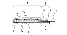
一般に、駆動ICを実装した液晶パネル(以下、COG液晶パネルという)は、図4に示すような断面構造となっている。このCOG液晶パネルは、液晶表示部Aと駆動IC実装部Bとで構成されている。液晶表示部Aは、上側ガラス基板1aと下側ガラス基板1bの対向する内面に配向膜で覆われたITO電極2a、コモン電極2bが形成され、液晶物質3を封止した構造となっている。駆動IC実装部Bは、下側ガラス基板1bが上側ガラス基板1aに比べて片側方向に大きく突き出ており、この下側ガラス基板1bの額縁部4上に配線パターン5が形成されると共に、この配線パターン5上に液晶を駆動するための駆動IC6と、外部からの信号の受け渡しをするためのケーブル7とが接合されている。配線パターン5は、ITO電極2a及びコモン電極2bとを相互に接続するパターン形状となっており、額縁部4に駆動IC6を実装する場合には、上側ガラス基板1aに形成したITO電極2aと導通部材を介して接続する構造となっている。
【0003】
上述のようなCOG液晶パネルの配線パターン5を形成するに当たっては、図5に示すように、まず、下側ガラス基板1bの額縁部4上に上記図4で示したITO電極2a及びコモン電極2bと電気的に接続された透明なITO電極膜5aの配線パターンを形成する。そして、電極としての抵抗値をより小さくするために、透明なITO電極膜5aの配線パターン上に駆動IC6を直接実装せずに、ITO電極膜5a上に導電性のよい金属電極被膜5cを形成し、この金属電極被膜5c上に駆動IC6を実装するものが多い。金属電極被膜5cの材質としては、導電性が良く且つ腐食性に優れた金や白金等の貴金属が使用されるが、このような貴金属は前記ITO電極膜5aに対して密着力が悪いため、一旦ITO電極膜5a上にクロム蒸着膜5bを形成し、このクロム蒸着膜5b上に前記金属電極被膜5cを形成する方法が多くとられていた。
【0004】
上記従来のCOG液晶パネルの配線パターン形成方法にあっては、駆動IC用配線パターンとITO電極パターンとの位置ずれを生じさせるおそれがあった。
また、下側ガラス基板1bのほぼ全面に金属電極被膜5cを形成するために、必要とする部分以外の金属電極被膜5cについては最終的に除去する面積が多くなり、金属材料が無駄に使われることにもなる。さらに、上記従来の配線パターン形成方法では、フォトマスクを2回被せるなど製造工程が多くなることから製造コストが高いものとなっていた。
【0005】
上記従来技術の問題点を解決するために、図6に示すようなCOG液晶パネルの配線パターン形成方法が開示されている(例えば、特許文献1参照。)。以下図面を用いて簡単に説明する。図6は、COG液晶パネルの配線パターンを示し、図6(a)は配線パターンの断面構造図、図6(b)は、図6(a)におけるB部の部分拡大平面図である。このCOG液晶パネルの配線パターン形成方法は、図6(a)に示すように液晶表示部が形成されるガラス基板1bの全面に液晶用のITO電極膜5aを形成し、このITO電極膜5a上の一部にガラス基板1b上に実装される駆動IC用の金属電極被膜5cを水金法によって形成し、前記ITO電極膜5a及び金属電極被膜5cの全面にフォトレジスト膜を形成し、その上から配線パターン像が形成されたフォトマスクを介して露光し、金属電極被膜5c及びITO電極膜5aの順にエッチングして不要なITO電極膜5a及び金属電極被膜5cをそれぞれ除去することにより、ガラス基板1b上にITO電極膜5aのパターン及び金属電極被膜5cのパターンを形成するものである。
【0006】
【特許文献1】
特開平11−194358号(第3−4頁、図1−図2)
【0007】
【発明が解決しようとする課題】
しかしながら、図6(a)に示す従来のCOG液晶パネルの配線パターン形成方法にあっては、エッチング工程おいてエッチング液にフォトレジスト膜が耐えられずサイドエッチングが発生する。このため金属電極被膜とITO電極膜とが重なっている部分において、オーバーエッチングが大きくなり、図6(b)に示すように金属電極被膜及びITO電極膜の幅が細くなり、この時のオーバーエッチング量bの値が10〜15μmなるという問題があった。
【0008】
そこで本発明は、フォトレジスト膜の耐薬品性を向上させることにより、エッチング工程におけるオーバーエッチング量を低減し、幅やピッチがが小さく密度が細かいパターンが形成できる液晶パネルの配線パターン形成方法を提供することを目的とする。
【0009】
【課題を解決するための手段】
上記課題を解決するために、本発明の請求項1に係る液晶パネルの配線パターン形成方法は、液晶表示部が形成されるガラス基板の全面に液晶用の透明電極膜を形成し、この透明電極膜上の一部にガラス基板上に実装される駆動IC用の金属電極被膜を水金法によって形成し、前記透明電極膜及び金属電極被膜の全面にフォトレジスト膜を形成し、その上から配線パターン像が形成されたフォトマスクを介して露光し、パターニングされたフォトレジスト膜を加熱処理し、金属電極被膜をエッチングして不要な金属電極被膜を除去し、その後再度フォトレジスト膜を加熱処理し、透明電極膜をエッチングして不要な透明電極膜を除去することを特徴とする。
【0010】
また、本発明の請求項2に係る液晶パネルの配線パターン形成方法は、液晶表示部が形成されるガラス基板の一部にガラス基板上に実装される駆動IC用の金属電極被膜を水金法によって形成し、この金属電極被膜を含むガラス基板の全面に液晶用の透明電極膜を形成し、この透明電極膜の全面にフォトレジスト膜を形成し、その上から配線パターン像が形成されたフォトマスクを介して露光し、パターニングされたフォトレジスト膜を加熱処理し、透明電極膜をエッチングして不要な透明電極膜を除去し、その後再度フォトレジスト膜を加熱処理し、金属電極被膜をエッチングして不要な金属電極被膜を除去することを特徴とする。
【0011】
【発明の実施の形態】
(第1の実施形態)
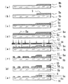
以下、図1、図2に基づいて本発明の第1の実施形態に係る配線パターン形成方法を詳細に説明する。図1は本実施形態に係る配線パターンを示し、図1(a)は配線パターンの断面構造図、図1(b)は図1(a)におけるA部の部分拡大平面図である。図2は本実施形態の製造工程を示す図である。
図1(a)に示すように、下側ガラス基板1bの額縁部4に透明電極膜としてのITO電極膜5aの配線パターンを形成し、その上に水金法によって直接に金属電極被膜5cを形成し、その上に駆動IC6を実装したものである。
次に、上記配線パターンの製造工程を図2に従って説明する。最初に蒸着装置を使用して、酸化インジウムに錫をドーピングして得られるITOを下ガラス基板1bの上面に蒸着してITO電極膜5aを形成する(工程a)。次に、有機金に酸化性の樹脂を混ぜ合わせてペーストを作り、このペーストで上記ITO電極膜5aの一部分にスクリーン印刷機を用いて金ペースト印刷膜8aを形成する(工程b)。有機溶剤は沸点が余り高くないのが好ましく、500℃程度で完全に樹脂分9が蒸発して残らないものを選択する。その状態のまま、焼成炉に入れて500℃位に加熱し、前記金ペースト印刷膜8aの樹脂分を完全に蒸発させる。
この樹脂分を完全に蒸発させることによって金だけが残り、この金がITO電極膜5aの表層に焼き付いて金属電極被膜5cが出来上がる(工程c)。このような上記工程b及び工程cによって金属電極被膜5cを形成する方法はいわゆる「水金法」とよばれるものである。
【0012】
次に、金属電極被膜5c及びITO電極膜5aの露出した表層面の全面にスクリーン印刷でポジ型のフォトレジスト膜10を形成する(工程d)。このフォトレジスト膜10は光照射によって分解して現像液に可溶性となり、現像時に基板表面から除去される特性をもつ感光性材料である。次に、配線パターン像を不透明に形成したポジ型のフォトマスク11を上記フォトレジスト膜10の上方に配置し、紫外線12を照射する(工程e)。フォトマスク11に形成された配線パターン像に相当するところは紫外線12がカットされ、パターン以外のところは紫外線12が透過してフォトレジスト膜10を溶解し、洗浄することによって溶解したフォトレジスト膜10が除去される一方、紫外線12が透過しないパターン部にはフォトレジスト膜10が残る。このようにしてフォトレジスト膜10が残っている下側ガラス基板1bを温度180℃で30分間保持しフォトレジスト膜10に加熱処理を施す。このようにフォトレジスト膜に加熱処理を施すことによってフォトレジスト膜のエッチング液に対する耐薬品性が向上する。次に、この下側ガラス基板1bを金属用のエッチング液に浸漬し、フォトレジスト膜10が取り除かれている所の金属電極被膜5cを除去する(工程f)。その後、再度フォトレジスト膜10を温度180℃で30分間保持して加熱処理を施し、ITO用のエッチング液に浸漬し、フォトレジスト膜10が取り除かれている所のITO電極膜5aを除去する(工程g)。このように、金属電極被膜5c、ITO電極膜5aの順にエッチング処理した後、表層面に残ったフォトレジスト膜10をレジスト剥離液に浸漬し除去することで配線パターンの製造が終了する(工程h)。
【0013】
以上、本実施形態の配線パターン形成方法によれば、エッチング処理の前にフォトレジスト膜10を温度180℃で30分間保持し加熱処理を施すことにより、フォトレジスト膜10の耐薬品性を向上させることができる。その結果、図1(b)に示すようにエッチング工程におけるオーバーエッチング量aの値を2〜3μmに低減することが出来る。
【0014】
(第2の実施形態)
図3は本発明の第2実施形態による配線パターン形成方法を示したものである。ここに示される方法は、前述の金や白金に比べて腐食し易い銀や銅等の金属材料を金属電極被膜として用いる場合に最適なものである。即ち、前述の第1の実施形態とは異なって、下側ガラス基板1bの上に先ず金属電極被膜5cを形成し、その上にITO電極膜5aを形成することで、金属電極被膜5cをITO電極膜5aで被い、金属電極被膜5cが外気に触れないようにすることで腐食を防止している。
【0015】
本実施形態に係る配線パターンは、以下の方法によって形成される。先ずガラス基板1bの額縁部4に相当する部分に銀粉入りのペーストをスクリーン印刷して銀ペースト印刷膜8bを形成する(工程a)。これを焼成炉において約500℃に加温し樹脂分9を蒸発させ、銀の金属電極被膜5cを形成する(工程b)。
次に上記金属電極被膜5cを含む下側ガラス基板の全表面に蒸着法でITO電極膜5aを形成する(工程c)。そして、ITO電極膜5aの全面にスクリーン印刷でポジ型のフォトレジスト膜10を形成し(工程d)、液晶表示部のコモン電極2bパターン(図4参照)と、駆動IC6(図1参照)が搭載される配線パターン像の形状を不透明に形成したポジ型のフォトマスク14を上記フォトレジスト膜10の上に配置し、紫外線12を上方より照射する。パターン部以外のところは紫外線が透過することでフォトレジスト膜10が分解し可溶性となるのでこれを除去する(工程e)。一方、紫外線12が透過しないパターン部にはフォトレジスト膜10が残る。このようにしてフォトレジスト膜10が残っている下側ガラス基板1bを温度180℃で30分間保持しフォトレジスト膜10に加熱処理を施す。このようにして形成されたガラス基板をITO用のエッチング液に浸漬し、ITO電極膜5aを除去する(工程f)。その後、再度フォトレジスト膜10を温度180℃で30分間保持して加熱処理を施し、銀用のエッチング液に浸漬し、金属電極被膜5cを除去する(工程g)。最後にレジスト剥離液に浸漬し、残ったフォトレジスト膜10を除去して製造工程を終了する(工程h)。
【0016】
本実施形態の形成方法による配線パターンの構造は、図3(h)に示したように、ITO電極膜5aの上面に駆動IC6が実装された構造となる。このときの電流抵抗値は、ITO電極膜5a自体が非常に薄いために特に大きくなることはなく、銀で形成した金属電極被膜5cに駆動IC6を直接接合した場合と同程度の抵抗値を得ることができる。また、本実施形態においても第1の実施形態と同様にエッチング工程におけるオーバーエッチング量aの値を2〜3μmに低減することが出来る。
【0017】
なお、上記いずれの実施例でもポジ型のフォトレジスト膜とポジ型のフォトマスクとを使用してパターン形成した場合について説明したが、本発明ではネガ型のフォトレジスト膜とネガ型のフォトマスクとの組み合わせによってもパターン形成できることは勿論である。
【0018】
【発明の効果】
以上説明したように、本発明に係るCOG液晶パネルの配線パターン形成方法によれば、フォトレジスト膜の耐薬品性が向上し、エッチング工程におけるオーバーエッチング量を低減することができる。これによって配線パターンの幅やピッチを小さくすることが可能となり、密度が細かい配線パターンを形成することができる。
【0019】
また、1回のフォトマスクによる露光で金属電極被膜及びITO電極膜のパターン形成を同時に行なえるため、駆動IC用配線パターンとITO電極用パターンとの位置ズレを防止することができる。また、駆動IC用配線パターンを形成する際に必要部分にのみ金属電極被膜を形成することで金属材料の無駄がなくなると共に、配線パターンの形成工程が簡素化でき、製造コストを低減することができる。
【0020】
また、本発明に係るCOG液晶パネルの配線パターン形成方法によれば、金属電極被膜を先に形成してからその上にITO電極膜を被覆形成することができるので、金属電極被膜を外気の影響から保護することができ、結果的に金や白金等の高価な材料以外の銀や銅といった金属材料も配線パターンとして使用することでコストを低減することが出来る。
【図面の簡単な説明】
【図1】本発明の第1の実施の形態における配線パターンを示し、図1(a)は配線パターンの断面構造図、図1(b)は図1(a)におけるA部の部分拡大平面図である。
【図2】本発明の第1の実施の形態における液晶パネルの製造工程を示す図である。
【図3】本発明の第2の実施の形態における液晶パネルの製造工程を示す図である。
【図4】従来技術における液晶パネルの断面図である。
【図5】従来技術の液晶パネルに形成される配線パターンの拡大断面図である。
【図6】従来技術における液晶パネルの配線パターンを示し、図6(a)はCOG液晶パネルの配線パターンの断面構造図、図6(b)は、図6(a)におけるB部の部分拡大平面図である。
【符号の説明】
1a 上側ガラス基板
1b 下側ガラス基板
2a ITO電極
2b コモン電極
3 液晶物質
4 額縁部
5 配線パターン
5a ITO電極膜
5c 金属電極被膜
6 駆動IC
7 ケーブル
8a 金ペースト印刷膜
8b 銀ペースト印刷膜
10 フォトレジスト膜
11 フォトマスク
12 紫外線
14 フォトマスク[0001]
BACKGROUND OF THE INVENTION
The present invention relates to a low resistance wiring pattern forming method for a liquid crystal panel in which a driving IC is mounted on a glass substrate on which a liquid crystal display unit is formed by a COG (Chip On Glass) method.
[0002]
[Prior art]
In general, a liquid crystal panel (hereinafter referred to as a COG liquid crystal panel) on which a driving IC is mounted has a cross-sectional structure as shown in FIG. The COG liquid crystal panel includes a liquid crystal display unit A and a drive IC mounting unit B. The liquid crystal display unit A has a structure in which an ITO electrode 2a and a common electrode 2b covered with an alignment film are formed on the inner surfaces of the upper glass substrate 1a and the lower glass substrate 1b facing each other, and the liquid crystal material 3 is sealed. . In the driving IC mounting portion B, the lower glass substrate 1b protrudes larger in one direction than the upper glass substrate 1a, and the wiring pattern 5 is formed on the frame portion 4 of the lower glass substrate 1b. A driving IC 6 for driving liquid crystal and a cable 7 for transferring signals from the outside are joined on the wiring pattern 5. The wiring pattern 5 has a pattern shape for connecting the ITO electrode 2a and the common electrode 2b to each other. When the driving IC 6 is mounted on the frame portion 4, the wiring pattern 5 is electrically connected to the ITO electrode 2a formed on the upper glass substrate 1a. It has a structure connected via a member.
[0003]
In forming the wiring pattern 5 of the COG liquid crystal panel as described above, as shown in FIG. 5, first, the ITO electrode 2a and the common electrode 2b shown in FIG. 4 are formed on the frame portion 4 of the lower glass substrate 1b. A wiring pattern of a transparent ITO electrode film 5a that is electrically connected to is formed. In order to further reduce the resistance value as an electrode, the metal electrode film 5c having good conductivity is formed on the ITO electrode film 5a without directly mounting the driving IC 6 on the wiring pattern of the transparent ITO electrode film 5a. In many cases, the driving IC 6 is mounted on the metal electrode coating 5c. As the material of the metal electrode coating 5c, a noble metal such as gold or platinum having good conductivity and excellent corrosiveness is used. However, since such noble metal has poor adhesion to the ITO electrode film 5a, There have been many methods in which a chromium vapor deposition film 5b is once formed on the ITO electrode film 5a and the metal electrode film 5c is formed on the chromium vapor deposition film 5b.
[0004]
In the conventional method for forming a wiring pattern of a COG liquid crystal panel, there is a risk of causing a positional shift between the driving IC wiring pattern and the ITO electrode pattern.
In addition, since the metal electrode coating 5c is formed on almost the entire surface of the lower glass substrate 1b, the area of the metal electrode coating 5c other than the necessary portion is finally removed, and the metal material is wasted. It will also be. Further, in the conventional wiring pattern forming method, the manufacturing cost is high because the manufacturing process is increased, such as covering the photomask twice.
[0005]
In order to solve the above-described problems of the prior art, a wiring pattern forming method for a COG liquid crystal panel as shown in FIG. 6 is disclosed (for example, see Patent Document 1). This will be briefly described below with reference to the drawings. FIG. 6 shows a wiring pattern of the COG liquid crystal panel, FIG. 6A is a sectional structural view of the wiring pattern, and FIG. 6B is a partially enlarged plan view of a portion B in FIG. In this COG liquid crystal panel wiring pattern forming method, as shown in FIG. 6A, a liquid crystal ITO electrode film 5a is formed on the entire surface of a glass substrate 1b on which a liquid crystal display portion is formed. A metal electrode film 5c for a driving IC to be mounted on a glass substrate 1b is formed on a part of the substrate by a water-gold method, and a photoresist film is formed on the entire surface of the ITO electrode film 5a and the metal electrode film 5c. The glass substrate is exposed to light through a photomask on which a wiring pattern image is formed, and the metal electrode film 5c and the ITO electrode film 5a are etched in this order to remove unnecessary ITO electrode film 5a and metal electrode film 5c, respectively. The pattern of the ITO electrode film 5a and the pattern of the metal electrode film 5c are formed on 1b.
[0006]
[Patent Document 1]
JP-A-11-194358 (page 3-4, FIGS. 1-2)
[0007]
[Problems to be solved by the invention]
However, in the conventional method of forming a wiring pattern for a COG liquid crystal panel shown in FIG. 6A, the photoresist film cannot withstand the etching solution in the etching process, and side etching occurs. For this reason, in the portion where the metal electrode film and the ITO electrode film overlap, overetching becomes large, and the widths of the metal electrode film and the ITO electrode film become narrow as shown in FIG. There was a problem that the amount b was 10 to 15 μm.
[0008]
Therefore, the present invention provides a method for forming a wiring pattern for a liquid crystal panel that can reduce the amount of over-etching in an etching process by improving the chemical resistance of a photoresist film, and can form a pattern with a small width and pitch and a small density. The purpose is to do.
[0009]
[Means for Solving the Problems]
In order to solve the above problems, a wiring pattern forming method for a liquid crystal panel according to claim 1 of the present invention comprises forming a transparent electrode film for liquid crystal on the entire surface of a glass substrate on which a liquid crystal display portion is formed. A metal electrode film for a driving IC to be mounted on a glass substrate is formed on a part of the film by a water-gold method, a photoresist film is formed on the entire surface of the transparent electrode film and the metal electrode film, and wiring is formed thereon. Exposure is performed through a photomask on which a pattern image is formed, the patterned photoresist film is heated, the metal electrode film is etched to remove unnecessary metal electrode films, and then the photoresist film is heated again. The transparent electrode film is etched to remove unnecessary transparent electrode films.
[0010]
According to a second aspect of the present invention, there is provided a wiring pattern forming method for a liquid crystal panel in which a metal electrode film for a driving IC mounted on a glass substrate is formed on a part of a glass substrate on which a liquid crystal display unit is formed. A transparent electrode film for liquid crystal is formed on the entire surface of the glass substrate including the metal electrode film, a photoresist film is formed on the entire surface of the transparent electrode film, and a wiring pattern image is formed thereon. Expose and heat the patterned photoresist film through the mask, etch the transparent electrode film to remove unnecessary transparent electrode film, then heat-treat the photoresist film again, and etch the metal electrode film An unnecessary metal electrode film is removed.
[0011]
DETAILED DESCRIPTION OF THE INVENTION
(First embodiment)
The wiring pattern forming method according to the first embodiment of the present invention will be described below in detail with reference to FIGS. FIG. 1 shows a wiring pattern according to the present embodiment, FIG. 1A is a sectional structural view of the wiring pattern, and FIG. 1B is a partially enlarged plan view of a portion A in FIG. FIG. 2 is a diagram showing the manufacturing process of this embodiment.
As shown in FIG. 1A, a wiring pattern of an ITO electrode film 5a as a transparent electrode film is formed on the frame part 4 of the lower glass substrate 1b, and a metal electrode coating 5c is directly formed thereon by a water-gold method. The driving IC 6 is mounted thereon.
Next, the manufacturing process of the wiring pattern will be described with reference to FIG. First, using an evaporation apparatus, ITO obtained by doping tin with indium oxide is evaporated on the upper surface of the lower glass substrate 1b to form an ITO electrode film 5a (step a). Next, an organic resin is mixed with an oxidizing resin to make a paste, and this paste is used to form a gold paste printed film 8a on a portion of the ITO electrode film 5a using a screen printer (step b). The organic solvent preferably has a boiling point that is not so high, and is selected so that the resin component 9 does not completely evaporate at about 500 ° C. In this state, it is put in a baking furnace and heated to about 500 ° C., and the resin content of the gold paste printed film 8a is completely evaporated.
By completely evaporating the resin component, only gold remains, and this gold is baked onto the surface layer of the ITO electrode film 5a to form the metal electrode film 5c (step c). Such a method of forming the metal electrode film 5c by the steps b and c is called a so-called “water-gold method”.
[0012]
Next, a positive photoresist film 10 is formed by screen printing on the entire exposed surface of the metal electrode film 5c and the ITO electrode film 5a (step d). The photoresist film 10 is a photosensitive material that has the property of being decomposed by light irradiation to become soluble in a developer and removed from the substrate surface during development. Next, a positive photomask 11 in which a wiring pattern image is formed opaque is placed above the photoresist film 10 and irradiated with ultraviolet rays 12 (step e). The portion corresponding to the wiring pattern image formed on the photomask 11 is cut off by the ultraviolet rays 12, and the portions other than the pattern are penetrated by the ultraviolet rays 12 to dissolve the photoresist film 10 and are dissolved by washing. While the photoresist film 10 is removed, the photoresist film 10 remains in the pattern portion through which the ultraviolet rays 12 are not transmitted. In this way, the lower glass substrate 1b on which the photoresist film 10 remains is held at a temperature of 180 ° C. for 30 minutes, and the photoresist film 10 is subjected to heat treatment. Thus, the chemical resistance with respect to the etching liquid of a photoresist film improves by heat-processing to a photoresist film. Next, this lower glass substrate 1b is immersed in a metal etching solution, and the metal electrode film 5c where the photoresist film 10 is removed is removed (step f). Thereafter, the photoresist film 10 is again heated for 30 minutes at a temperature of 180 ° C., and is subjected to heat treatment, and is immersed in an etching solution for ITO, thereby removing the ITO electrode film 5a where the photoresist film 10 is removed ( Step g). As described above, after the metal electrode coating 5c and the ITO electrode film 5a are etched in this order, the photoresist film 10 remaining on the surface layer is immersed in a resist stripping solution and removed to complete the production of the wiring pattern (step h). ).
[0013]
As described above, according to the wiring pattern forming method of this embodiment, the chemical resistance of the photoresist film 10 is improved by holding the photoresist film 10 at a temperature of 180 ° C. for 30 minutes and performing the heating process before the etching process. be able to. As a result, as shown in FIG. 1B, the value of the overetching amount a in the etching process can be reduced to 2 to 3 μm.
[0014]
(Second Embodiment)
FIG. 3 shows a wiring pattern forming method according to the second embodiment of the present invention. The method shown here is optimal when a metal material such as silver or copper, which is more easily corroded than the aforementioned gold or platinum, is used as the metal electrode coating. That is, unlike the above-described first embodiment, the metal electrode film 5c is first formed on the lower glass substrate 1b, and the ITO electrode film 5a is formed thereon. Corrosion is prevented by covering the electrode film 5a so that the metal electrode film 5c does not come into contact with the outside air.
[0015]
The wiring pattern according to this embodiment is formed by the following method. First, a paste containing silver powder is screen-printed on a portion corresponding to the frame portion 4 of the glass substrate 1b to form a silver paste printed film 8b (step a). This is heated to about 500 ° C. in a baking furnace to evaporate the resin component 9 to form a silver metal electrode coating 5c (step b).
Next, an ITO electrode film 5a is formed by vapor deposition on the entire surface of the lower glass substrate including the metal electrode coating 5c (step c). Then, a positive photoresist film 10 is formed by screen printing on the entire surface of the ITO electrode film 5a (step d), and a common electrode 2b pattern (see FIG. 4) of the liquid crystal display unit and a driving IC 6 (see FIG. 1) are formed. A positive type photomask 14 in which the shape of the mounted wiring pattern image is made opaque is disposed on the photoresist film 10 and irradiated with ultraviolet rays 12 from above. Except for the pattern portion, the photoresist film 10 is decomposed and becomes soluble due to the transmission of ultraviolet rays, which is removed (step e). On the other hand, the photoresist film 10 remains in the pattern portion through which the ultraviolet rays 12 are not transmitted. In this way, the lower glass substrate 1b on which the photoresist film 10 remains is held at a temperature of 180 ° C. for 30 minutes, and the photoresist film 10 is subjected to heat treatment. The glass substrate thus formed is immersed in an etching solution for ITO to remove the ITO electrode film 5a (step f). Thereafter, the photoresist film 10 is again heated at a temperature of 180 ° C. for 30 minutes, subjected to heat treatment, immersed in an etching solution for silver, and the metal electrode coating 5c is removed (step g). Finally, it is immersed in a resist stripping solution, and the remaining photoresist film 10 is removed to complete the manufacturing process (step h).
[0016]
The wiring pattern structure according to the forming method of the present embodiment is a structure in which the driving IC 6 is mounted on the upper surface of the ITO electrode film 5a as shown in FIG. The current resistance value at this time is not particularly large because the ITO electrode film 5a itself is very thin, and a resistance value comparable to that obtained when the drive IC 6 is directly joined to the metal electrode film 5c formed of silver is obtained. be able to. Also in the present embodiment, the value of the overetching amount a in the etching process can be reduced to 2 to 3 μm as in the first embodiment.
[0017]
In any of the above-described embodiments, the case where a pattern is formed using a positive photoresist film and a positive photomask has been described. However, in the present invention, a negative photoresist film and a negative photomask are used. Of course, the pattern can also be formed by a combination of the above.
[0018]
【The invention's effect】
As described above, according to the wiring pattern forming method for a COG liquid crystal panel according to the present invention, the chemical resistance of the photoresist film can be improved, and the amount of overetching in the etching process can be reduced. As a result, the width and pitch of the wiring pattern can be reduced, and a wiring pattern with a fine density can be formed.
[0019]
In addition, since the pattern formation of the metal electrode film and the ITO electrode film can be simultaneously performed by exposure with one photomask, it is possible to prevent the positional deviation between the drive IC wiring pattern and the ITO electrode pattern. In addition, by forming the metal electrode film only on the necessary portion when forming the wiring pattern for the driver IC, the metal material is not wasted, the wiring pattern forming process can be simplified, and the manufacturing cost can be reduced. .
[0020]
In addition, according to the method for forming a wiring pattern of a COG liquid crystal panel according to the present invention, an ITO electrode film can be formed on the metal electrode film after the metal electrode film is formed first. As a result, it is possible to reduce costs by using a metal material such as silver or copper other than expensive materials such as gold and platinum as a wiring pattern.
[Brief description of the drawings]
FIG. 1 shows a wiring pattern according to a first embodiment of the present invention, FIG. 1 (a) is a cross-sectional structure diagram of the wiring pattern, and FIG. FIG.
FIG. 2 is a diagram showing a manufacturing process of the liquid crystal panel in the first embodiment of the present invention.
FIG. 3 is a diagram showing a manufacturing process of a liquid crystal panel in a second embodiment of the present invention.
FIG. 4 is a cross-sectional view of a liquid crystal panel in the prior art.
FIG. 5 is an enlarged cross-sectional view of a wiring pattern formed in a conventional liquid crystal panel.
6A and 6B show a wiring pattern of a liquid crystal panel in the prior art, FIG. 6A is a cross-sectional structure diagram of the wiring pattern of a COG liquid crystal panel, and FIG. 6B is a partial enlarged view of a portion B in FIG. It is a top view.
[Explanation of symbols]
DESCRIPTION OF SYMBOLS 1a Upper glass substrate 1b Lower glass substrate 2a ITO electrode 2b Common electrode 3 Liquid crystal substance 4 Frame part 5 Wiring pattern 5a ITO electrode film 5c Metal electrode film 6 Drive IC
7 Cable 8a Gold paste printing film 8b Silver paste printing film 10 Photoresist film 11 Photomask 12 Ultraviolet light 14 Photomask