JP2004236469A - Instantaneous high power supply - Google Patents
Instantaneous high power supply Download PDFInfo
- Publication number
- JP2004236469A JP2004236469A JP2003024182A JP2003024182A JP2004236469A JP 2004236469 A JP2004236469 A JP 2004236469A JP 2003024182 A JP2003024182 A JP 2003024182A JP 2003024182 A JP2003024182 A JP 2003024182A JP 2004236469 A JP2004236469 A JP 2004236469A
- Authority
- JP
- Japan
- Prior art keywords
- power
- secondary battery
- power supply
- system bus
- converter
- Prior art date
- Legal status (The legal status is an assumption and is not a legal conclusion. Google has not performed a legal analysis and makes no representation as to the accuracy of the status listed.)
- Granted
Links
Images


Classifications
-
- B—PERFORMING OPERATIONS; TRANSPORTING
- B60—VEHICLES IN GENERAL
- B60L—PROPULSION OF ELECTRICALLY-PROPELLED VEHICLES; SUPPLYING ELECTRIC POWER FOR AUXILIARY EQUIPMENT OF ELECTRICALLY-PROPELLED VEHICLES; ELECTRODYNAMIC BRAKE SYSTEMS FOR VEHICLES IN GENERAL; MAGNETIC SUSPENSION OR LEVITATION FOR VEHICLES; MONITORING OPERATING VARIABLES OF ELECTRICALLY-PROPELLED VEHICLES; ELECTRIC SAFETY DEVICES FOR ELECTRICALLY-PROPELLED VEHICLES
- B60L3/00—Electric devices on electrically-propelled vehicles for safety purposes; Monitoring operating variables, e.g. speed, deceleration or energy consumption
- B60L3/0023—Detecting, eliminating, remedying or compensating for drive train abnormalities, e.g. failures within the drive train
- B60L3/0069—Detecting, eliminating, remedying or compensating for drive train abnormalities, e.g. failures within the drive train relating to the isolation, e.g. ground fault or leak current
-
- B—PERFORMING OPERATIONS; TRANSPORTING
- B60—VEHICLES IN GENERAL
- B60L—PROPULSION OF ELECTRICALLY-PROPELLED VEHICLES; SUPPLYING ELECTRIC POWER FOR AUXILIARY EQUIPMENT OF ELECTRICALLY-PROPELLED VEHICLES; ELECTRODYNAMIC BRAKE SYSTEMS FOR VEHICLES IN GENERAL; MAGNETIC SUSPENSION OR LEVITATION FOR VEHICLES; MONITORING OPERATING VARIABLES OF ELECTRICALLY-PROPELLED VEHICLES; ELECTRIC SAFETY DEVICES FOR ELECTRICALLY-PROPELLED VEHICLES
- B60L1/00—Supplying electric power to auxiliary equipment of vehicles
- B60L1/02—Supplying electric power to auxiliary equipment of vehicles to electric heating circuits
- B60L1/04—Supplying electric power to auxiliary equipment of vehicles to electric heating circuits fed by the power supply line
- B60L1/06—Supplying electric power to auxiliary equipment of vehicles to electric heating circuits fed by the power supply line using only one supply
-
- B—PERFORMING OPERATIONS; TRANSPORTING
- B60—VEHICLES IN GENERAL
- B60L—PROPULSION OF ELECTRICALLY-PROPELLED VEHICLES; SUPPLYING ELECTRIC POWER FOR AUXILIARY EQUIPMENT OF ELECTRICALLY-PROPELLED VEHICLES; ELECTRODYNAMIC BRAKE SYSTEMS FOR VEHICLES IN GENERAL; MAGNETIC SUSPENSION OR LEVITATION FOR VEHICLES; MONITORING OPERATING VARIABLES OF ELECTRICALLY-PROPELLED VEHICLES; ELECTRIC SAFETY DEVICES FOR ELECTRICALLY-PROPELLED VEHICLES
- B60L50/00—Electric propulsion with power supplied within the vehicle
- B60L50/50—Electric propulsion with power supplied within the vehicle using propulsion power supplied by batteries or fuel cells
- B60L50/51—Electric propulsion with power supplied within the vehicle using propulsion power supplied by batteries or fuel cells characterised by AC-motors
-
- B—PERFORMING OPERATIONS; TRANSPORTING
- B60—VEHICLES IN GENERAL
- B60L—PROPULSION OF ELECTRICALLY-PROPELLED VEHICLES; SUPPLYING ELECTRIC POWER FOR AUXILIARY EQUIPMENT OF ELECTRICALLY-PROPELLED VEHICLES; ELECTRODYNAMIC BRAKE SYSTEMS FOR VEHICLES IN GENERAL; MAGNETIC SUSPENSION OR LEVITATION FOR VEHICLES; MONITORING OPERATING VARIABLES OF ELECTRICALLY-PROPELLED VEHICLES; ELECTRIC SAFETY DEVICES FOR ELECTRICALLY-PROPELLED VEHICLES
- B60L50/00—Electric propulsion with power supplied within the vehicle
- B60L50/50—Electric propulsion with power supplied within the vehicle using propulsion power supplied by batteries or fuel cells
- B60L50/60—Electric propulsion with power supplied within the vehicle using propulsion power supplied by batteries or fuel cells using power supplied by batteries
- B60L50/64—Constructional details of batteries specially adapted for electric vehicles
-
- B—PERFORMING OPERATIONS; TRANSPORTING
- B60—VEHICLES IN GENERAL
- B60L—PROPULSION OF ELECTRICALLY-PROPELLED VEHICLES; SUPPLYING ELECTRIC POWER FOR AUXILIARY EQUIPMENT OF ELECTRICALLY-PROPELLED VEHICLES; ELECTRODYNAMIC BRAKE SYSTEMS FOR VEHICLES IN GENERAL; MAGNETIC SUSPENSION OR LEVITATION FOR VEHICLES; MONITORING OPERATING VARIABLES OF ELECTRICALLY-PROPELLED VEHICLES; ELECTRIC SAFETY DEVICES FOR ELECTRICALLY-PROPELLED VEHICLES
- B60L58/00—Methods or circuit arrangements for monitoring or controlling batteries or fuel cells, specially adapted for electric vehicles
- B60L58/10—Methods or circuit arrangements for monitoring or controlling batteries or fuel cells, specially adapted for electric vehicles for monitoring or controlling batteries
- B60L58/18—Methods or circuit arrangements for monitoring or controlling batteries or fuel cells, specially adapted for electric vehicles for monitoring or controlling batteries of two or more battery modules
- B60L58/20—Methods or circuit arrangements for monitoring or controlling batteries or fuel cells, specially adapted for electric vehicles for monitoring or controlling batteries of two or more battery modules having different nominal voltages
-
- Y—GENERAL TAGGING OF NEW TECHNOLOGICAL DEVELOPMENTS; GENERAL TAGGING OF CROSS-SECTIONAL TECHNOLOGIES SPANNING OVER SEVERAL SECTIONS OF THE IPC; TECHNICAL SUBJECTS COVERED BY FORMER USPC CROSS-REFERENCE ART COLLECTIONS [XRACs] AND DIGESTS
- Y02—TECHNOLOGIES OR APPLICATIONS FOR MITIGATION OR ADAPTATION AGAINST CLIMATE CHANGE
- Y02T—CLIMATE CHANGE MITIGATION TECHNOLOGIES RELATED TO TRANSPORTATION
- Y02T10/00—Road transport of goods or passengers
- Y02T10/60—Other road transportation technologies with climate change mitigation effect
- Y02T10/70—Energy storage systems for electromobility, e.g. batteries
Landscapes
- Engineering & Computer Science (AREA)
- Power Engineering (AREA)
- Transportation (AREA)
- Mechanical Engineering (AREA)
- Life Sciences & Earth Sciences (AREA)
- Sustainable Development (AREA)
- Sustainable Energy (AREA)
- Control Of Motors That Do Not Use Commutators (AREA)
- Inverter Devices (AREA)
- Supply And Distribution Of Alternating Current (AREA)
- Secondary Cells (AREA)
- Electric Propulsion And Braking For Vehicles (AREA)
Abstract
Description
【0001】
【発明の属する技術分野】
本発明は、短時間であれば、定格を超える大電力が供給可能な瞬時大電力供給装置に関する。
【0002】
【従来の技術】
近年、パーソナルコンピュータや精密モータを搭載した精密電子機器などのように、電源電圧の変動に敏感なエレクトロニクス機器が多用されてきている。このため、電源電圧が数秒以下の短時間大幅に低下する現象である瞬時電圧低下(以下、「瞬低」と略記する)に対する対策の要求が高まってきている。瞬時電圧低下対策の装置としては電圧の低下時のみに短時間大電力を供給できる電力安定供給装置があり、これの需要が増大しつつある。また従来から用いられている負荷平準化装置、ピークカット装置、周波数変動抑制装置、電圧安定化装置、フリッカー対策装置などの各種の電力安定供給装置に対しても、瞬時電圧低下対策のために短時間ではあるが大電力を供給する能力(以下、「瞬時大電力供給能力」という)を付加することが求められている。さらに、電熱装置や、多数の大型電球を用いた照明装置などでも瞬時大電力供給能力が要求される。すなわち電熱装置や照明装置の運転開始時にはコイルヒータの温度が低いので、定常運転動作時に比べて抵抗が低い。そのため大電流が流れその電力変換装置には瞬時大電力供給能力が要求される。
【0003】
また金属熱処理用の誘導加熱装置などでは金属部品などを高精度の温度制御の下で迅速に熱処理するために、運転開始時に低温状態にある加熱炉を急速に所定の高い温度にしたり急速に所定の低い温度にすることが必要となる。このため定常運転状態で高温を維持する場合に比べて、運転開始時には大きな電力が必要となる。このような短時間ではあるが大電力を供給する必要がある場合の電力を「瞬時大電力」といい、瞬時大電力を供給するための装置を「瞬時大電力供給装置」という。モータなども運転開始時には静止状態から回転を始めるため大電力を必要とし、モータ用の電力変換装置には瞬時大電力供給能力が要求される。電気自動車などでは、発進時やタイヤがぬかるみに入り込んだ際に脱出する場合などには、短時間ではあるが通常の走行時よりも大きな電力でモータを駆動する必要がある。このように瞬時大電力を必要とする負荷装置は多種多様である。以下に、従来の瞬時大電力供給装置である電力安定供給装置を例に挙げ従来の技術について説明する。上記負荷平準化装置、ピークカット装置などの電力安定供給装置、電熱装置、照明装置、モータ装置などの負荷が定常状態で動作している時を以下「通常時」という。
【0004】
図10は二次電池108としてレドックスフロー電池を用いた従来の電力安定供給装置101を有する電力供給系統のブロック図である。図において、変電所130の電力系統100に変圧器120を介して系統母線102が連結されている。電力安定供給装置101はこの系統母線102に開閉器103を介して連系されている。系統母線102には、例えば重要負荷104及び105がそれぞれの開閉器114、115を経て接続されている。重要負荷104、105は、例えば半導体製造工場、精密機械加工工場など、特に安定な電力供給が必要な大口需要家の重要な設備である。系統母線102には開閉器109、111を介して一般負荷110も接続されている。電力安定供給装置101は、主に連系リアクトルを兼ねる変圧器106、交流電力を直流電力に変換し、又はその逆の変換をするコンバータ107及び大容量の二次電池108(レドックスフロー電池)を備えている。この電力安定供給装置101は、通常時はピークカット装置や負荷平準化装置として機能するが、雷事故の発生などによる瞬低時には重要負荷104、105の稼働停止などを防止するための瞬時電圧低下防止対策装置としても働く。
【0005】
以下、電力安定供給装置101の機能を詳細に説明する。変電所130と、重要負荷104、105及び一般負荷110とを結ぶ電力供給系統の電力の需給が均衡を保っている状態である「定常時」には、系統母線102から開閉器103及び変圧器106を経て交流電力が電力安定供給装置101に供給される。交流電力はコンバータ107で直流電力に変換されて二次電池108に蓄電される。重要負荷104又は105の消費電力が大幅に増加して、一時的に負荷104、105に供給される電力が変電所130の容量を超過する場合には、電圧検出器10を有する検出回路8により、その状態が検出される。検出回路8の検出出力は制御回路9に与えられる。制御回路9はコンバータ107を制御して、二次電池108の放電による直流電力をコンバータ107で交流電力に変換し、上記の超過する分の有効電力を系統母線102に供給して需給を安定化させる。変電所130から系統母線102へ供給されるべき超過分の電力を電力安定供給装置101が代りに供給して、系統母線102の供給電力のピークをカットできるのでこの機能を「ピークカット」と呼んでいる。
【0006】
電力安定供給装置101の二次電池108の容量を大きくし長時間供給できる電力を蓄電できるようにすると負荷平準化装置として使用できる。すなわち、夜間の低需要時間帯に一定時間(典型的には約8時間)定電力で二次電池108に蓄電し、昼間の高需要時間帯には一定時間(典型的には約8時間)定電力で二次電池108から電力を供給する。これにより、高需要時間帯には変電所130の供給可能電力以上の電力を供給できる。この用途の電力安定供給装置は、昼と夜の電力需要の大きなギャップを平準化するので「負荷平準化装置」と呼ばれている。
【0007】
電力系統100に雷が到来して系統の電圧に瞬低が生じた場合には、電圧検出器10が瞬低を検出する。瞬低による重要負荷104、105の稼働停止などを防ぐために、直ちに瞬低前の系統電圧に復帰させる必要がある。そのために、電力安定供給装置101は、制御回路9によりコンバータ107を制御して、二次電池108から重要負荷104、105にコンバータ107及び系統母線102を経由して無効電力や有効電力を供給して電力の安定供給を維持する。二次電池108からの供給電力が不十分なときは開閉器109を開き重要度の低い一般負荷110を切り離し、少なくとも重要負荷104、105だけには所望の電力を供給して重要負荷104、105の稼働停止を防ぐようにしている。瞬低が回復すると直ちにコンバータ107は通常時の動作状態に戻り、変電所130から電力を供給する。
【0008】
従来の電力安定供給装置においては、ピークカット時や負荷平準化時には、例えばそれぞれ前者では500kW、後者では2MW程度の電力を比較的長時間(例えば、前者では約1時間、後者は約8時間)供給することが必要とされる。ピークカットや負荷平準化の動作時に雷が到来して瞬低が発生した時には、低下した電圧の復帰のために比較的短時間(例えば、2秒間)ではあるが1MWから数MWの電力を追加供給する必要がある。
【0009】
【特許文献1】
特開2002−84683号公報
【特許文献2】
特開平11−32438号公報
【特許文献3】
国際公開番号WO98/43301
【特許文献4】
国際公開番号WO00/22679
【特許文献5】
特開2000−252475号公報
【0010】
【発明が解決しようとする課題】
電熱装置、電球を用いた照明装置、モータなどの起動時に瞬時大電力を必要とする負荷が接続されている配電線は通常瞬時大電力供給能力を有している。自動車用のヒータや電球、モータに電力を供給する二次電池や電気自動車用の燃料電池なども瞬時大電力供給能力を有している。また、電力安定供給に用いるレドックスフロー電池、ナトリウム硫黄電池、鉛電池などの二次電池は、数秒から数分の短時間であれば定格よりはるかに大きな電流を供給できる「瞬時大電流供給能力」を有している。すなわち数秒から数分間であれば通常時に供給できる定格電流の数倍程度の電流を供給できる。瞬時大電力を必要とするときにこの能力を活用すれば、二次電池の定格容量を瞬時大電力に相当する容量にまで増大しなくても瞬時大電力を供給できる。しかし、前記従来の電力安定供給装置の電力変換装置であるコンバータ107のスイッチング素子として用いられているシリコン(Si)の半導体素子は、定格の数倍を超える電力を制御する能力を有していない。そこでコンバータ107の定格電力を瞬時大電力にほぼ等しい値に設定しておく必要がある。従って通常時では定格電力の数分の1の電力で使用することになる。
【0011】
電熱装置及び電球を用いた照明装置などの運転開始時に、コイルヒータの温度が上昇して定常状態になるまでの時間、或いはモータが起動して所定の回転状態に達するまでの時間は、全運転時間に比べると極めて短い時間である。また電力安定供給装置において、雷の到来による瞬低はそれほど頻繁に発生するものではなく、多くても年間20回程度である。また雷の影響による瞬低の持続時間は多重雷の場合でも数秒間である。まれではあるが送電線にへびや鳥などの小動物がひっかかったり、樹木が接したりして短絡や地絡が発生することがある。このような場合には数分を超える比較的長時間の「瞬時停電」が起こることもある。しかしこのように短時間の瞬低や瞬時停電時の瞬時大電力に対応するために、通常時の電力の数倍にも及ぶ電力定格を有する大型のコンバータなど電力変換装置を設けることは、瞬時大電力供給装置が大型化し設備費が高くつくばかりでなく、維持費も高くつくという問題があった。
【0012】
本発明は、制御電極による制御で通常時と瞬時大電力を必要とする時とで動作モードを選択的に変えられる半導体素子を用いる。これによって通常時に必要な電力に相当する電力定格を有する電力変換装置を用いながら、装置始動時や瞬低、瞬時停電の発生時には通常時の電力を大幅に超える電力を供給できる電力変換装置を有する、小型・軽量・低コストの瞬時大電力供給装置を提供することを目的とする。
【0013】
【課題を解決するための手段】
本発明の瞬時大電力供給装置に設けられる電力変換装置は、ゲート電圧がゲート接合のビルトイン電圧よりも低い時はユニポーラ半導体素子として機能し、高い時はバイポーラ半導体素子として機能する、ユニポーラ半導体素子の機能とバイポーラ半導体素子の機能を合わせもつ半導体素子(以下、「複合機能半導体素子」という)をスイッチング素子として用いる。電力系統が定格電力以下の電力で動作している通常時には、複合機能半導体素子をユニポーラ半導体素子として動作させる。瞬低時や瞬時大電力が必要な、各種装置(負荷)が始動する運転開始時(以下、「装置始動時」という)にはバイポーラ半導体素子として動作させる。これにより、通常時には電力変換装置が定格電力で動作し、瞬低時や装置始動時などの瞬時大電力供給時には定格電力を大幅に超える電力で動作する。大電力供給時間は短いので半導体素子が破壊されることはない。
本発明の瞬時大電力供給装置は、直流電力を充放電する二次電池、及び前記二次電池と、電力送電電源の系統母線との間に接続され、前記系統母線から入力される交流を直流に変換して前記二次電池に出力し、前記二次電池から出力される直流を交流に変換して前記系統母線に出力する電力変換装置として、スイッチング素子が複合機能半導体素子で構成された電力変換装置であるコンバータを有する。
【0014】
複合機能半導体素子は、定格電力以下で動作する時はユニポーラ動作をする。バイポーラ動作時には、短時間であればユニポーラ動作時の定格電力の1.5から20倍の電力を制御することができる。高性能のヒートシンクを用いた場合、数分間であれば定格電力の1.4から5倍の電力を制御できる。本発明では、コンバータのスイッチング素子に用いる複合機能半導体素子のユニポーラ動作時の定格電力を負荷が定常状態で動作している「通常時」の値に設定しておく。短時間に大電力を供給する必要がある瞬低時(雷の発生などにより電源電圧が数秒以下の短時間大幅に低下したとき)や瞬時停電時(数分を超える比較的長時間の停電が発生した時)には、通常時の定格電力を大幅に超えるバイポーラ動作時の電力で電力変換装置であるコンバータを動作させる。バイポーラ動作時にはユニポーラ動作時に比べてゲート駆動電流が大きくなり、ゲート電流による損失が大幅に増加する。しかしバイポーラ動作は短時間であるのでこれによる電力損失の増大は実用上無視できるレベルである。
【0015】
本発明の他の観点の瞬時大電力供給装置は、直流電流を充放電する二次電池、前記二次電池に接続され、二次電池の充電電圧を降圧し、二次電池の放電電圧を昇圧する双方向のチョッパー回路、及び
前記チョッパー回路と電力送電電源の系統母線との間に接続され、前記系統母線から入力される交流を直流に変換してチョッパー回路に出力し、前記チョッパー回路から入力される直流を交流に変換して前記系統母線へ出力するスイッチング素子が複合機能半導体素子で構成された電力変換装置であるコンバータを有する。
本発明の瞬時大電力供給装置では、双方向のチョッパー回路により二次電池の充電電圧を降圧し、放電電圧を昇圧するので、前記の効果に加えて、二次電池の電圧より高い電圧を有する系統母線にも瞬時大電力供給装置を適用することができる。
【0016】
本発明の他の観点の瞬時大電力供給装置は、直流電力を充放電する二次電池、前記二次電池に接続され、二次電池の充電電圧を降圧し、二次電池の放電電圧を昇圧する双方向のチョッパー回路、
前記チョッパー回路と電力送電電源の系統母線との間に接続され、前記系統母線から入力される交流を直流に変換してチョッパー回路に出力し、前記チョッパー回路から入力される直流を交流に変換して前記系統母線へ出力するスイッチング素子が複合機能半導体素子で構成された電力変換装置であるコンバータ、
前記系統母線の電圧を検出し、検出した電圧に基づいて電力の需給状態を検出する検出装置、及び前記検出装置の検出出力に基づいて、前記系統母線に接続された負荷と電力送電電源との電力の需給が均衡しているとき、前記二次電池を充電し、需要が供給を上回ったとき、前記二次電池を放電して電力を系統母線へ供給するよう前記コンバータを制御する制御回路を有する。
本発明によれば、上記の効果に加えて、系統母線の電圧を検出することにより瞬低の発生を検出して、二次電池から系統母線への電力を供給して瞬低時の系統の電圧低下を防ぐことができる。
【0017】
本発明の他の観点の瞬時大電力供給装置は、直流電力を充放電する二次電池、前記二次電池に接続され、二次電池の充電電圧を降圧し、二次電池の放電電圧を昇圧する双方向のチョッパー回路、
前記チョッパー回路と電力送電電源の系統母線との間に接続され、前記系統母線から入力される交流を直流に変換してチョッパー回路に出力し、前記チョッパー回路から入力される直流を交流に変換して前記系統母線へ出力するスイッチング素子が複合機能半導体素子で構成された電力変換装置であるコンバータ、
前記系統母線の電圧及び電流を検出し、検出した電圧及び電流に基づいて前記負荷の電力の需給状態を検出する検出装置、及び
前記検出装置の検出出力に基づいて、前記系統母線に接続された負荷と電力送電電源との電力の需給が均衡しているとき、前記二次電池を充電し、需要が供給を上回ったとき、前記二次電池を放電して電力を系統母線へ供給するよう前記コンバータを制御する制御回路を有する。
本発明によれば、上記の効果に加えて、系統母線の電圧と電流を検出することにより、系統の電力の需給状況を検出することができる。電力の需給状況を検出できるので、本発明の瞬時大電力供給装置を負荷平準化用に用いることができる。
【0018】
本発明の他の観点の瞬時大電力供給装置は、前記系統母線の電圧が雷事故などの発生により短時間大幅に低下する瞬低時には、前記二次電池から、前記二次電池の定格放電電力の2倍から12倍の放電電力を出力させ、前記コンバータが、コンバータの定格制御電力の2倍から12倍に相当する前記二次電池の放電電力を交流に変換して所定の無効電力と定格電力の2から12倍の有効電力を系統母線に出力するように、前記制御回路により制御されることを特徴とする。
前記系統母線の電圧の瞬低時には、前記二次電池から、前記二次電池の定格放電電力の2倍から12倍の放電電力を出力させ、前記コンバータが、コンバータの定格制御電力の2倍から12倍に相当する前記二次電池の放電電力を交流に変換して所定の無効電力と定格電力の2倍より小さい有効電力を系統母線に出力するように、前記制御回路により制御されることを特徴とする。
前記系統母線とコンバータとの間に連系リアクトルを設けたことを特徴とする。
前記二次電池が、レドックスフロー電池又はナトリウム硫黄電池であることを特徴とする。
【0019】
前記複合機能半導体素子が、シリコンカーバイド(SiC)を母材とする電荷注入型接合電界効果トランジスタ(CIJFET)であることを特徴とする。
前記複合機能半導体素子が、窒化ガリウムを母材とする半導体素子であることを特徴とする。
前記複合機能ワイドギャップバイポーラ半導体素子が、SiCのCIJFETの少なくとも1つのチップ又は複数のチップを並列に接続したもので形成されていることを特徴とする。
【0020】
前記ワイドギャップバイポーラ半導体素子が、SiCのCIMOSFETの少なくとも1つのチップ又は複数のチップを並列に接続したもので形成されていることを特徴とする。
本発明の他の観点の瞬時大電力供給装置は、直流電力を充放電する二次電池、前記二次電池に接続され、前記二次電池の充電電圧を降圧し、前記二次電池の放電電圧を昇圧する双方向のチョッパー回路、
前記チョッパー回路と電力送電電源の系統母線との間に接続され、前記系統母線から入力される交流を直流に変換してチョッパー回路に出力し、前記チョッパー回路から入力される直流を交流に変換して前記系統母線へ出力するスイッチング素子が複合機能半導体素子で構成された電力変換装置であるコンバータ、
前記系統母線の周波数を検出し、検出した周波数に基づいて、電力の需給状態を検出する検出装置、及び
前記検出装置の検出出力に基づいて、前記系統母線に接続された負荷と、電力送電電源との電力の需給が均衡しているとき、前記二次電池を充電し、需要が供給を上回ったとき、前記二次電池を放電して電力を系統母線へ供給するよう前記コンバータを制御する制御回路を有する。
【0021】
本発明の他の観点の瞬時大電力供給装置は、直流電力を充放電する二次電池、及び前記二次電池と、電力送電電源の系統母線に接続された負荷との間に接続され、スイッチング素子としてワイドギャップバイポーラ半導体素子を備え、前記系統母線から入力される交流を直流に変換して前記二次電池に出力し、前記二次電池から出力される直流を交流に変換して前記負荷に出力する電力変換装置であるコンバータを有する。
この瞬時大電力供給装置は、さらに、前記系統母線に接続された負荷に供給される電力の電圧及び電流を検出し、検出した電圧及び電流に基づいて、前記負荷の電力の需給状態を検出する検出装置、及び前記検出装置の検出出力に基づいて、前記負荷と、電力送電電源との電力の需給が均衡しているとき、前記二次電池を充電し、需要が供給を上回ったとき、前記二次電池を放電して電力を系統母線へ供給するよう前記コンバータを制御する制御回路を有する。
【0022】
本発明の他の観点の瞬時大電力供給装置は、直流電力を供給する直流電源、及び前記直流電源と負荷との間に接続され、スイッチング素子として、制御電極による制御によってユニポーラ半導体素子として動作させるかバイポーラ半導体素子として動作させるかが選択される複合機能を有し、通常時はユニポーラ半導体素子として動作し、瞬時大電力を必要とするときはバイポーラ半導体素子として動作する複合機能半導体素子を有し、前記直流電源から入力される直流電力を交流電力に変換して前記負荷に出力する電力変換装置を備える。
前記直流電源が、電力系統の交流を直流に変換する整流装置と、前記整流装置の直流の正負出力端間に接続されたコンデンサを有することを特徴とする。
前記直流電源が二次電池又は燃料電池であることを特徴とする。
前記複合機能半導体素子が、シリコンカーバイド(SiC)を母材とする、電荷注入型接合電界効果トランジスタ(CIJFET)又は電荷注入型MOS電界効果トランジスタ(CIMOSFET)のいずれか一方であることを特徴とする。
【0023】
【発明の実施の形態】
以下に本発明の実施の形態について説明する。
本発明の、複合機能半導体素子をスイッチング素子として用いた電力変換装置を有する瞬時大電力供給装置では、通常時に複合機能半導体素子をユニポーラ半導体素子として動作させ、瞬低時や、負荷となる装置の運転開始時(装置始動時)など、瞬時大電力が必要な時にはバイポーラ半導体素子として動作させる。これにより、通常時には電力変換装置は定格電力で動作し低損失である。瞬低時や装置始動時には損失は大きくなるが定格電力を大幅に超える電力で動作させることができる。
特に、SiC(シリコンカーバイド)、GaN(窒化ガリウム)、ダイヤモンドなどを母材としたワイドギャップ半導体素子は、Si(シリコン)を母材とした半導体素子に比べて損失が著しく少なく、且つ高温でも動作できるという物理的性質を有している。この点に注目してワイドギャップ半導体素子で制御できる短時間の最大許容電力を調べたところ、数秒間程度の短時間であればワイドギャップ半導体素子に定格電流をはるかに超える電流を流しても破壊されないことが判った。特にワイドギャップバイポーラ半導体素子は二次電池の「瞬時大電流供給能力」を大幅に越える大電流を流すことができる「瞬時大電力稼働能力」をもつことが確認された。
【0024】
本発明における電力変換装置(コンバータ)では、通常時にユニポーラ半導体素子として動作し、瞬低時や瞬時大電力が必要な装置始動時にはバイポーラ半導体素子として動作するワイドギャップ複合機能半導体素子をスイッチング素子として用い、通常時はワイドギャップユニポーラ半導体素子の定格内の電圧及び電流で動作させる。瞬低時や装置始動時には、二次電池の瞬時大電流供給能力により通常時の数倍の直流電力を放電させ、前記コンバータの複合機能半導体素子をバイポーラ半導体素子として動作させてこの直流電力を交流電力に変換し、電熱装置、照明装置、モータ装置などに電力を供給する。
【0025】
二次電池の電圧が系統母線の電圧より低い場合には、二次電池の放電による直流出力電圧はチョッパー回路で昇圧された後、コンバータで交流電力に変換されて系統母線に出力される。二次電池は「通常時」に充電される。二次電池の充電時は、系統母線からの交流電力がコンバータで直流電力に変換され、チョッパー回路で降圧されて二次電池に充電される。通常時に充放電される電力値はコンバータの定格内にある。
【0026】
瞬低時又は瞬時停電時には、二次電池の瞬時大電流供給能力に応じて定格の数倍の電流が、ほぼ二次電池の定格電圧を保ちつつ供給される。すなわち、二次電池から定格電力のほぼ数倍の直流電力が供給される。この直流電力はチョッパー回路で昇圧された後にコンバータで交流電力に変換されて系統母線に出力され、電力の供給を安定化する。
コンバータでは、複合機能半導体素子のスイッチング素子に対して一般的な既知のPWM動作型のスイッチング制御を行いパルス幅変調をする。このパルス幅変調式のコンバータ(以下、PWMコンバータと記す)の出力電圧の位相を系統母線の電圧の位相よりも進ませて通常時と同じ電力を系統母線に出力することにより、有効電力を系統母線に出力するのが電力安定供給のために望ましい。瞬低時には系統母線の電圧が低下するのでパルス幅変調のパルス幅を広げてコンバータを動作させる。これにより、通常時の数倍の無効電力を系統母線に出力し、低下した電圧を瞬低前の電圧に急速に戻す。
【0027】
小電力制御用の、炭化珪素(SiC)などを母材とするワイドキャップ複合機能半導体素子は1つの半導体チップを用いて構成することができる。しかし大電力制御用のワイドギャップ複合機能半導体素子は1つの半導体チップで構成するのは難しい。その理由は、ワイドギャップ半導体素子の母材のSiCには多くの結晶欠陥が存在するために、大面積の半導体チップを欠陥のない状態で作るのが難しいからである。特に本発明の用途のような大電流を流すことができる面積の大きいチップの作製は困難である。SiCの結晶欠陥を減少させる技術が向上すればSiと同程度の大面積のチップの半導体素子が実現できるが、現状では大電流を流すためには複数のチップを並列に接続している。
【0028】
従来の瞬時大電力供給装置に設けられているSiのバイポーラトランジスタ又はSiのIGBTを用いた従来のコンバータでは、Siのバイポーラトランジスタ又はSiのIGBTの定格容量を、瞬低時や運転開始時に二次電池から供給される通常時の数倍の電力に合わせた容量に設定しなければならない。
これに対して本発明の瞬時大電力供給装置では、SiCのCIJFET又はSiCのCIMOSFETが複合機能を有しているので、これを用いたコンバータは、定格電流の数倍の大電流を制御できる。従ってコンバータのスイッチング素子である複合機能半導体素子の定格電流を通常時の電流に合わせてコンバータを設定しても瞬低時の大電流時に対応できる。電力安定供給装置などの瞬時大電力供給装置を構成する種々の部品、例えばリアクトルとしてのトランス、半導体素子のヒートシンク、ブスバーなどが小型にできる。また、定格容量が小さいので、同じ変換効率でも損失の絶対値が小さく低損失化ができるとともに大幅な低コスト化も達成できる。電力用途の大型コンバータは、小型のコンバータに比べて高耐圧であるとともに高い信頼性が求められる。また多くの保護機能を要求されるので価格が高い。例えば従来の瞬時大電力供給装置で5MWのコンバータが必要である用途の場合、本発明のものでは1MWのもので済む。このためにコストは従来のもののほぼ5分の1になり大幅な低コスト化が達成できる。電力容量の大きい瞬時大電力供給装置ほど低コスト化の効果が大きくなる。
【0029】
以下、本発明の瞬時大電力供給装置の好適な実施例を図1から図7を参照して説明する。
《第1実施例》
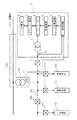
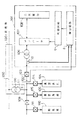
図1は、本発明の第1実施例であるピ−クカット用の瞬時大電力供給装置1、及びこの瞬時大電力供給装置1が接続された、変電所130から重要負荷104、105及び一瞬負荷110に至る電力供給系統のブロック図である。「ピークカット」とは、電力需要の急増により、消費電力が変電所130の供給可能な電力を超過するとき、変電所130以外の電源から超過分を供給することをいい、この状態にあるときを「ピークカット時」という。またピークカット時以外の状態のときを「定常時」という。図において、変電所130の電力系統100にトランス120を経て系統母線102が連結されている。系統母線102には、特に重要な重要負荷104及び105がそれぞれの開閉器114及び115を介して接続されている。また、系統母線102には開閉器109及び111を介して重要負荷104、105より重要度の低い一般負荷110が接続されている。開閉器109は系統母線102に異常が発生したとき、まず一般負荷110を切り離して、重要負荷104、105への電力供給を優先して維持するためのものである。系統母線102には、本発明の瞬時大電力供給装置1が開閉器6を介して接続されている。開閉器6、109、111、114及び115を動作させる制御装置については、当分野では周知であるので図示を省略している。
【0030】
瞬時大電力供給装置1は例えば500kW定格のレドックスフロー電池を用いた定格電圧が3.2kVの二次電池2、500kW定格のコンバータ4及び、連系リアクトルも兼ねた変圧器5を有し、開閉器6を介して6.6kVの系統母線102に連結されている。系統母線102の電圧と電流は、それぞれ電圧検出器10及び電流検出器11で検出され、検出した電圧、電流に基づいて電力の需給状態が検出回路8で検出される。電圧検出器10にはポテンシャルトランス(PT)などが用いられる。電流検出器11はカレントトランス(CT)などであり、変電所130内に設けられて変電所130の出力電流を検出する。制御回路9には、検出回路8から与えられる電力の需給状態を示す検出出力に応じてモード切替回路13が出力する制御信号が入力され、それに応じた駆動信号をコンバータ4に印加して出力電力を制御する。二次電池2のレドックスフロー電池は電圧800Vの場合には、図2に示すように二次電池2とコンバータ4の間に双方向のチョッパー回路3を設けて、充電電圧を降圧し、放電電圧を昇圧する。二次電池2は電圧800V、電流625Aの直流を約1時間供給できる容量を有する。チョッパー回路3及びコンバータ4のスイッチング素子は電荷注入型接合電界効果トランジスタ(以下、CIJFETと記す)である。チョッパー回路3のCIJFETの定格電圧は8kV、定格電流は800Aであり、コンバータ回路4のCIJFETの定格電圧は8kV,定格電流は400Aである。本装置の電力容量はチョッパー回路3、コンバータ4及び変圧器5で発生する電力損失を考慮すると約450kWである。
【0031】
重要負荷104、105の電力消費が増えて一時的に変電所130の出力電力容量を超過する場合には、電圧検出器10及び電流検出器11がその状態を検出し、瞬時大電力供給装置は検出回路8、モード切替回路13、制御回路9を経てコンバータ4を制御し、二次電池2から系統母線102に向けて超過電力に相当する有効電力を最大約450kWまで供給できる。二次電池2は変電所130と、重要負荷104、105及び一般負荷110などとの間の電力の需給が均衡を保っている定常時に系統母線102から供給される電力により充電されている。
【0032】
レドックスフロー電池などの二次電池2の直流の出力電圧は、使用期間の初期には例えば800Vであるが、使用期間が長くなるとともに800Vより低下する傾向がある。そこで、ピ−クカット時は定電圧出力保持型のチョッパー回路3で二次電池2の出力電圧を昇圧し電圧を常に一定にしてコンバータ4に供給するのが望ましい。
【0033】
直流電力を交流電力に変換し又は交流電力を直流電力に変換するコンバータ4は、SiCを母材とする複合機能半導体素子であるSiC−CIJFETをスイッチング素子として用いている。コンバータ4は、一般的な既知の回路構成を有するものであるので図示を省略している。SiC−CIJFETはSiCの結晶内の欠陥による制約のために、電流定格を大きくするのが困難である。そこで電圧定格を高くして低い電流定格において所望の電力定格を得るのが望ましい。この場合図2に示すように、二次電池2のレドックスフロー電池の出力電圧800Vをチョッパー回路3で3.2kVに昇圧して、約3.2kV、300Aの直流電力をコンバータ4に供給している。コンバータ4ではこの直流電力を交流電力に変換して変圧器5に印加する。変圧器5は3.2kVの電圧を6.6kVに昇圧して開閉器6を経て系統母線102に出力し負荷104、105及び110に供給する。
【0034】
ピークカット時に瞬時大電力供給装置1が450kWのピ−クカット時電力を供給しているとき、もし電力系統100に落雷事故が発生し、その影響で系統母線102の電圧に瞬時電圧低下(瞬低)が生じると、電圧検出器10により検出される。瞬低は重要負荷104、105に稼働停止などの重大な障害を与えるおそれがある。そこでこれを防ぐために、直ちに開閉器109を開き一般負荷110を切り離す。同時に瞬時大電力供給装置1において、電圧検出器10の検出出力が検出回路8に入力される。検出回路8はこの検出出力に基づいて制御回路9の動作モードを決める指令信号を生成してモード切替回路13に印加する。モード切替回路13は、コンバータ4のSiC−CIJFETをユニポーラ半導体素子として動作させるか、バイポーラ半導体素子として動作させるかの動作モードを決める制御信号を制御回路9に印加する。制御回路9は入力された制御信号によりコンバータ4のスイッチング素子であるSiC−CIJFETをPWM制御するPWM制御信号をコンバータ4に入力する。制御回路9は、二次電池2からその瞬時大電流供給能力に相当する、例えば電圧が800Vで、2.5MWの直流電力が出力されるようにコンバータ4を制御する。チョッパ回路3は800Vの直流電圧を3.2kVに昇圧してコンバータ4に供給する。コンバータ4では制御回路9によりSiC−CIJFETのゲート電圧が増大され、SiC−CIJFETはユニポーラ動作からバイポーラ動作に切り替わる。その結果、コンバータ4からは、電圧が1.47kVで450kWの有効電力と、電圧が約1.47kVで、2.78MVAR(無効電力の単位を表す)の無効電力が出力される。
【0035】
有効電力及び無効電力の電圧は変圧器5で6.6kVに昇圧されて系統母線102に供給されて電圧低下を防ぐ。落雷の影響による系統母線102の電圧低下が0.5秒間以上続くのは極めて稀である。本実施例の瞬時大電力供給装置1は450kWの有効電力と最大2.78MVARの無効電力を約6秒間供給できるようにコンバータ4を設計してあるので、落雷による瞬低の対策として十分である。上記の例ではコンバータ4は4秒間であれば定格の約6倍の瞬時大電力を変換することができる。
本実施例の瞬時大電力供給装置を瞬低のみに対応させる場合には、図10に示す従来の電力供給安定装置のように、電圧を検出する電圧検出器10のみを設ければよい。
【0036】
次に本実施例の瞬時大電力供給装置1に用いる複合機能半導体素子のSiC−CIJFETについて詳しく説明する。本実施例において定格を大幅に越える電力でコンバータ4を動作させることができるのは、スイッチング素子として複合機能半導体素子であるSiC−CIJFETを用いているからである。
図3の(a)は、本実施例で用いている、定格電圧及び電流が8kV・400AのSiC−CIJFET素子(モジュール)の上面図であり、図3の(b)は(a)のb−b断面図である。このSiC−CIJFET素子は、定格電流45AのSiC−CIJFETチップ131〜139を9個並列に接続してモジュール化している。図3の(b)において、ソース電極14の上に9個の中間下部電極16を設け、各中間下部電極16の上に一辺が7mmの略正方形の9個のCIJFETチップ131〜139を設けている。各CIJFETチップ131〜139の上に中間上部電極17を設けている。すべての中間上部電極17に接してドレイン電極15を設け、ソース電極14とドレイン電極15で9個のCIJFETチップ131〜139を挟んでいる。この構成により9個のCIJFETチップ131〜139はソース電極14とドレイン電極15間で並列に接続される。各CIJFETチップ131〜139の間には、スペーサ18が設けられ、カソード電極14の上における各CIJFETチップ131〜139の位置を定めている。セラミックス外囲器19はソース電極14とドレイン電極15間を一定距離に保持すると共に絶縁するものであり、その直径は約10cmである。
【0037】
図4にSiCのCIJFETセルの断面を示し、図5に出力特性を示す。複数のCIJFETセルを並列配置して1つのCIJFETチップが構成される。図4において、CIJFETセルはn型SiCの、ドレインとして機能する基板50の上面にn型ドリフト層51を設けている。n型ドリフト層51の上部領域にp型埋込ゲート層521を形成し、両端部領域にそれぞれp型埋込ゲート層522、523を形成している。p型埋込ゲート層521はn型チャネル層53を挟んでn型ソース層54に対向している。n型ソース層54にはソース電極56が設けられている。p型埋込ゲート層522、523のそれぞれに接してp型上部ゲート層524、525が形成され、p型上部ゲート層524、525には制御電極であるゲート電極57が設けられている。基板50の下面にドレイン電極55を設けている。p型埋込ゲート層521、522、523及びp型上部ゲート層524、525はゲート端子59に電気的に接続されている。
【0038】
図4のCIJFETセルにおいて、ドレイン電極55を高電位、ソース電極56を低電位にした状態で、制御電極であるゲート電極57に印加するゲート電圧をソース電極56と同電位にしたとき、p型上部ゲート層524、525とp型埋込ゲート層521との間のn型チャネル層53がゲートpn接合周辺の空乏層で完全に覆われCIJFETセルはピンチオフする。そのためドレイン電極55とソース電極56間には電流が流れず高い逆耐電圧を保つ。ゲート電極57に、ゲートpn接合のビルトイン電圧(約2.7V)よりも小さい範囲でソース電極56の電圧より高いゲート電圧を印加すると、CIJFET素子131はユニポーラ半導体素子として動作する。すなわち、空乏層によるピンチオフが解消されてn型チャネル層53にチャネルが形成され、ドレインとしての基板50からn型ソース層54に向けて電子による電流が流れる。ゲート電圧を大きくすると空乏層の幅が狭くなるので、逆にチャネルの幅が広くなりより大きな電流が流れる。
【0039】
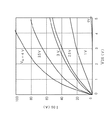
図5はゲート電圧VG をパラメータとした、ドレイン・ソース間の電圧電流特性を示す。図5に示すように、ゲート電圧VG が2.5Vでは、ドレイン・ソース間電圧VDSが4Vのとき、ドレイン・ソース間電流IDSは定格電流の45Aとなる。ゲート電極57にゲートpn接合のビルトイン電圧(約2.7V)よりも大きいゲート電圧を印加するとCIJFETチップ131はバイポーラ半導体素子として動作する。すなわち、p型埋込ゲート層521、522、523及びp型上部ゲート層524、525から正孔がn型チャネル層53に注入され、n型チャネル層53で伝導度変調が生じる。このためn型チャネル層53の抵抗が著しく低下する。さらに、n型ソース層54及びn型チャネル層53からp型埋込ゲート層521に電子が注入され、この電子がp型埋込ゲート層521の中を拡散してn型ドリフト層51に達する。このようになるとp型埋込ゲート層521がp型ベース領域として機能し、CIJFETはnpnトランジスタと同様の動作をする。そのため正孔による電流と電子による電流による大きな電流がドレイン電極55からソース電極56に流れる。例えばドレイン・ソース間電圧VDSが4Vでゲート電圧VG が4Vの時、定格電流の約2.2倍の100Aのドレイン・ソース間電流IDSが流れる。
【0040】
上記の特性を有するCIJFETを用いたコンバータ4を備える瞬時大電力供給装置1のピークカット時の動作を以下に説明する。ピークカット時には、CIJFETのゲート電極57にゲートpn接合のビルトイン電圧(2.7V)よりも小さいゲート電圧を印加し、CIJFETをユニポーラ半導体素子として動作させる。瞬低時にはビルトイン電圧よりも大きいゲート電圧を印加してバイポーラ半導体素子として動作させ、約6秒間であればユニポーラ半導体素子として動作していた場合の約3.5倍の大電流を流すことができる。
【0041】
シリコン(Si)を母材とするSi−バイポーラ半導体素子はバイポーラ動作で負の温度依存性を持つ。従って大電流が流れて素子の内部温度が上昇すると更に電流が増えて益々温度が上昇し、ついには熱暴走して素子の破壊にいたる。複数のSi−バイポーラチップを並列に接続した場合は、あるSi−バイポーラチップに一旦電流集中が起こると、他のSi−バイポーラチップの電流もそのチップに集中してしまい熱暴走にいたる場合がある。従ってSi−バイポーラチップを多数並列に接続して使用するのは困難である。
【0042】
これに対して、SiC−CIJFETの内部抵抗は正の温度依存性をもつ。従って過大な電流が流れて素子温度が上がると内部抵抗が増加して電流が自動的に低減されて温度上昇が抑制され、熱暴走にいたることはない。大電流の流れる時間が10秒以下であれば多数のSiC−CIJFETチップを並列に接続して使用可能である。大電流を流せる時間は、各チップの内部での発生熱量が放熱量より大きいためチップの内部温度が上昇し、半導体としての性質を維持できる限界温度にいたるまでの時間である。この時間は各チップの構造や通電電流の密度、チップを並列に接続したモジュールの構造などに依存して決まる。図3に示す構成では定格の約3倍の電流を流す場合約6秒間は全く問題を生じないことが実験により確認された。例えば、約45分間のピークカットの動作試験をしている間に8秒間の瞬低を発生させるテストをしたが、重要負荷104、105にほとんど影響を及ぼすことなくピークカット及び瞬低時に十分対応可能な電力を供給できた。
【0043】
本実施例のコンバータは、スイッチング素子として用いるSiC−CIJFETの瞬時大電力稼働能力を活用することにより、瞬低の影響を防止するのに必要な約4.5秒間は定格電力の約6倍の電力を変換するコンバータとして働く。従って、従来のシリコンの半導体素子を用いたコンバータのように、コンバータの容量の設計値を瞬低時を考慮に入れた大電力のものにする必要はない。前記容量の設計値はピークカット時の電力が供給できる能力、すなわち瞬低時の電力の数分の1の電力を供給できる容量で十分である。これにより、ピークカットに対応可能な瞬時大電力供給装置の大幅な小型化・軽量化・低コスト化が実現できる。
【0044】
《第2実施例》
図6は、本発明の第2実施例である負荷平準化用の瞬時大電力供給装置21のブロック図である。瞬時大電力供給装置21は定格電圧1.5KV、定格電力1.5MWのナトリウム硫黄電池を用いた二次電池22、双方向のチョッパー回路23、コンバータ24及び変圧器25を有しており、前記図1の瞬時大電力供給装置1と同様に、開閉器6を介して、電圧6.6KVの系統母線102に接続されている。その他の構成は瞬時大電力供給装置1と同じである。本実施例において、瞬時大電力供給装置21は負荷平準化用の電力安定供給装置として働く。
【0045】
「負荷平準化」とは、電力の需要が1日の中の時間帯により大幅に異なる現象に対処するために、電力需要の少ない時間帯に電力を蓄積し、需要の多い時間帯に蓄積した電力を放出することをいう。電力需要の少ない夜間の、例えば22時から6時の8時間に二次電池22を一定電力で充電する。電力需要の特に多い昼間の、例えば9時から17時の8時間は約1.35MWの電力を二次電池22から供給する。チョッパー回路23のスイッチング素子(図示省略)は、電圧・電流が10kV・1400AのSiC−電荷注入型MOS電界効果トランジスタ(以下、CIMOSFETと記す)である。またコンバータ24のスイッチング素子(図示省略)は、電圧・電流が10kV・600AのSiC−CIMOSFETである。SiC−CIMOSFETは、ワンチップで定格電流の大きなものを作るのが難しく、1つのSiC−CIMOSFETチップを流すことができる電流は40A程度である。本実施例のコンバータ22に用いるSiC−CIMOSFET素子(モジュール)は、定格電流40AのCIMOSFETチップを図3に示すものと類似のパッケージ内に15個設け、それらを並列接続してモジュール化している。
【0046】
上記のように、SiC−CIMOSFETは定格電流が比較的小さいので、電圧を高くして定格電力を大きくする。例えば、昼間に1.35MWの電力を供給している時は、チョッパー回路23で二次電池2の1.5kVの直流出力電圧を3kVに昇圧している。その結果、コンバータ4には電圧・電流が約3kV・480Aの直流電力が供給される。コンバータ24はこの直流電力を電圧・電流が約1.38kV・566Aの交流電力に変換して変圧器25に供給する。変圧器25は1.38kVの電圧を6.6kVに昇圧し、開閉器6を介して系統母線102に供給している。
【0047】
1.35MWの電力を供給している時に電力系統100に落雷事故による瞬低が発生し、その影響で系統母線102の電圧が大幅に低下すると、電圧の低下が電圧検出器10で検出され、検出出力が検出回路8に入力される。検出回路8は検出出力に基づいて動作モードを決める指令信号生成してモード切替回路13に印加する。モード切替回路13はコンバータ4のSiC−CIMOSFETをユニポーラ半導体素子として動作させるかバイポーラ半導体素子として動作させるかの動作モードを決める制御信号を制御回路9に印加する。制御回路9は入力された制御信号によりPWM制御信号を生成してコンバータ24に入力し、コンバータ24のスイッチング素子を駆動する。二次電池22の出力電圧はチョッパー回路23で4.5kVに昇圧されてコンバータ24に供給される。制御回路9はスイッチング制御のPWM信号のパルス幅を拡大した駆動信号をコンバータ24に印加する。これによりコンバータ24から、定格値である約1.35MWの有効電力と、電圧が約2.07kVで約6.44MVARの無効電力が出力される。コンバータ24の出力は変圧器25で昇圧されて系統母線102に供給され系統母線102の電圧低下を防ぐ。
【0048】
本実施例の瞬時大電力供給装置において、上記のように定格を大幅に超える電力でコンバータを動作させることができるのは、スイッチング素子としてSiC−CIMOSFETを用いているからである。
図7にSiC−CIMOSFETのセルの断面図を示す。SiC−CIMOSFETはn型SiCのドレインとして機能する基板150の上にn型ドリフト層151を形成している。n型ドリフト層151の上部中央領域にはp型ゲート層652を形成している。ドリフト層151の上部の両端部領域にそれぞれp型ゲート層653、654を形成している。両p型ゲート層653、654の上に他のp型ゲート層655、656をそれぞれ形成している。p型ゲート層652、653、654で囲まれた領域にn型チャネル層658が形成されている。n型チャネル層658の上部中央領域にn型ソース層659が形成されている。基板150の下面にドレイン電極160が設けられ、n型ソース層659にソース電極161が設けられている。p型ゲート層655、656にそれぞれp型ゲート電極661、662が設けられている。n型チャネル層658にMOSゲート絶縁層665、666を介してそれぞれMOSゲート電極667、668が設けられている。p型ゲート層652、653、654、655、656はp型ゲート電極661、662に電気的に接続されp型ゲート端子670として導出されている。MOSゲート電極667と668は電気的に接続され、MOSゲート端子673として導出されている。
【0049】
CIMOSFETのセルにおいて、ドレイン電極160を高電位、ソース電極161を低電位にして電圧を印加した状態で、MOSゲート電極667、668とp型ゲート電極661、662に印加するゲート電圧をソース電極161と同電位にしたとき、n型チャネル層658はゲートpn接合周辺の空乏層で完全に覆われSiC−CIMOSFETはピンチオフする。その結果、ドレイン電極160とソース電極161の間に電流が流れず高い耐電圧を有する。MOSゲート電極667、668に所定の閾値以上のゲート電圧を印加し、p型ゲート電極661、662にゲートpn接合のビルトイン電圧(約2.7V)よりも小さい範囲でソース電極161の電圧より高いゲート電圧を印加すると、SiC−CIMOSFETはユニポーラ半導体素子として動作する。すなわち、空乏層によるピンチオフが解消されてn型チャネル層658にチャネルが形成され、ドレイン電極160からソース電極161に向かう電子による電流が流れる。p型ゲート電極661、662に印加するゲート電圧を大きくすると空乏層の幅が狭くなるので、逆にチャネルの幅が広くなりドレイン電極160とソース電極161間により大きな電流が流れる。
【0050】
p型ゲート電極661、662にゲートpn接合のビルトイン電圧(2.7V)よりも大きい電圧を印加すると、CIMOSFETはバイポーラ半導体素子として動作する。すなわち、p型ゲート層652、653、654、655、656からn型チャネル層658に正孔が注入されn型チャネル層658で伝導度変調が発生して、n型チャネル層658の抵抗が著しく低減する。また、n型ソース層659及びn型チャネル層658からp型ゲート層652に電子が注入される。この電子がp型ゲート層652の中を拡散してn型ドリフト層151に達する。このようにしてp型ゲート層652がp型ベースの機能を果たしてCIMOSFETはnpnトランジスタの動作をし、正孔による電流と電子による大きな電流がドレイン電極160からソース電極161に流れる。
本実施例の図6に示す瞬時大電力供給装置21のチョッパー回路23とコンバータ24のスイッチング素子は、SiC−CIMOSFETの複数のセルから構成されたチップを15個並列に接続し、図3に示すものと類似のモジュールに構成したものを用いている。モジュールにおいて、15個のチップの、MOSゲート電極667、668が共通に接続され、p型ゲート電極661、662、p型ゲート層652が共通に接続される。また15個のチップの、ドレイン電極160が共通に接続され、ソース電極161が共通に接続される。
【0051】
本実施例の瞬時大電力供給装置を瞬低用に用いる時は、CIMOSFETのp型ゲート電極661、662にゲートpn接合のビルトイン電圧(約2.7kV)よりも大きいゲート電圧を印加してバイポーラ半導体素子として動作させる。バイポーラ半導体素子として動作させる時間が約5秒間であれば、ユニポーラ半導体素子として動作する場合の約3.8倍の大電流を流すことができる。
本実施例ではSiC−CIMOSFETの瞬時大電力稼働能力を活用することにより、定格電力1.5MWのコンバータを、瞬低の影響を防ぐ短時間であれば1.5MWの約4.7倍の、定格電力が約7MWに相当するコンバータとして動作させることができる。従って、大幅に小型化・軽量化・低コスト化された、瞬低時にも対応可能な負荷平準化用の瞬時大電力供給装置を実現できる。
【0052】
《第3実施例》
本発明の第3実施例を図8を参照して説明する。
図8は本発明の瞬時大電力供給装置を、100kW、500Hz級の誘導加熱装置に適用した例のブロック図を示す。金属製の部品などを高精度の温度管理の下で迅速に熱処理するための加熱装置では、運転開始時や運転中に低温の加熱炉を急速に所定の高温にしたり、逆に高温の加熱炉を急速に所定の低温にすることが必要とされる。特に運転開始時には、定常運転状態で所定の高温を維持するときに比べて大きな電力が必要となる。
【0053】
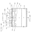
図8において、3相の配電系統線290に開閉器292を経て整流器301が接続され、入力の3相交流が整流されて直流出力端子295、296に直流出力が得られる。直流出力端子295、296間には大容量のコンデンサ302が接続され、直流出力はコンデンサ302を充電する。直流出力端子295、296間にはインバータ303が接続されている。インバータ303の出力端子315、316はそれぞれのコンデンサ317、318を経て加熱コイル304の両端子319、320にそれぞれ接続されている。加熱コイル304の近傍には加熱炉内の温度を検出する温度センサ306が設けられ、検出出力は検出回路309に入力されている。整流器301の3相の入力線の2本にCTなどの電流検出器307、308が設けられ、検出出力は検出回路309に入力されている。
【0054】
インバータ303の出力端子315につながる出力線にも電流検出器305が設けられており、検出出力は検出回路309に入力されている。検出回路309の出力はモード切替回路300に印加される。モード切替回路300は、スイッチング素子331〜334をユニポーラ半導体素子として動作させるかバイポーラ半導体素子として動作させるかの動作モードを判定して、モード制御信号を制御回路310に入力する。制御回路310の4つの出力端はインバータ303の駆動回路311、312、313、314の各入力端に接続されている。駆動回路311、312、313、314の出力端はそれぞれスイッチング素子331、332、333、334のゲートに接続されている。各スイッチング素子331〜334のソース・ドレイン間には、よく知られているフライホイーリング用のダイオードが接続されている。
インバータ303において、スイッチング素子331、332、333、334は、定格電圧・電流が1kV・150AのCIJFETモジュールで構成されている。CIJFETモジュールの構成は図3に示す第1実施例のものに類似である。インバータ303は、整流器301の直流出力を交流出力に変換し、コンデンサ317、318を経て誘導加熱コイル304に供給している。
【0055】
検出回路309は、電流検出器305、307、308の検出出力及び温度検出器306の検出出力に基づいて所定の演算処理を行い、結果の指令信号をモード切替回路300に印加する。モード切替回路300はこの指令信号に基づいて動作モードを決めるモード制御信号を制御回路310に印加する。制御回路310はモード制御信号に応じて4つの制御信号を生成し、それぞれ駆動回路311〜314に印加する。各駆動回路311〜314は入力された制御信号に基づいて各スイッチング素子331〜334の駆動信号を生成し、各スイッチング素子に印加する。
【0056】
誘導加熱装置は、熱処理する金属部品の材質、形状、使用目的に応じて加熱炉内の温度を所定時間(例えば5秒〜30秒)で所定の温度まで上昇させる必要がある。従って通常は誘導加熱装置の運転開始時には大電力を供給する必要がある。本実施例では運転開始時には、スイッチング素子331〜334のCIJFETをそれぞれの駆動回路311〜314の駆動信号によりバイポーラ半導体素子として動作させ、定常時の3倍から5倍の交流出力電力を加熱コイル304に供給することができる。定常時にはCIJFETをユニポーラ半導体素子として動作させ、CIJFETでの電力損失を防ぐのが望ましい。コンデンサ302に大容量のものを用いれば、加熱コイル304への供給電力が急増した場合にコンデンサ302に充電された電荷が供給電力の急増分を補う。これにより供給電力の急増による配電系統線290の電圧の低下を防ぐことができる。
【0057】
本実施例によれば、誘導加熱装置のインバータ303の定格出力を、定常運転時の出力に合わせて設定しておけばよく、運転開始時や急加熱時など短時間に大出力を要する時には、スイッチング素子331〜334のCIJFETをバイポーラ半導体素子として動作させることによって定常時の3〜5倍の出力を得ることができる。従って誘導加熱装置の小型化、軽量化、低コスト化が実現できる。
【0058】
《第4実施例》
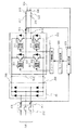
本発明の第4実施例を図9を参照して説明する。図9は本発明の瞬時大電力供給装置を定格出力60kWの電気自動車の走行用モータ404に適用した例のブロック図である。走行用モータ404に印加する交流の定格周波数は例えば18kHzである。
【0059】
図9において、バッテリ401に電源スイッチ400を介して電力変換装置である3相のインバータ403が接続されている。バッテリ401の両端子間にはコンデンサ402が接続されている。バッテリ401は鉛電池などの二次電池であるが、燃料電池などの発電装置であってもよい。
インバータ403の3つの出力端415、416、417には永久磁石のロータを有するシンクロナスモータであるモータ404が接続されている。モータ404のロータの回転角を、ロータに連結されたシャフトの近傍に設けたシャフト回転角検出器405で検出し、シャフトの回転速度を表す検出信号が検出回路408に入力される。モータ404のステータ電流はCTなどの電流検出器420により検出され、検出信号が検出回路408に入力される。検出回路408にはさらに、運転者のアクセルペダルの操作に応じて出力されるトルク要求信号407が入力されている。検出回路408は入力された両検出信号及びトルク要求信号に基づいて演算処理を行い、結果の処理信号をモード切替回路410に入力する。モード切替回路410はスイッチング素子431〜436の動作モードを決めるモード制御信号をインバータ制御回路409に印加する。制御回路409はインバータ403のスイッチング素子431、432、433、434、435、436を駆動するそれぞれの駆動回路421、422、423、424、425、426に制御信号を出力する。駆動回路421〜426は入力される制御信号に基づいてスイッチング素子431〜436を駆動する駆動信号をそれぞれのスイッチング素子431〜436の制御電極であるゲートに印加する。各スイッチング素子431〜436のソース・ドレイン間には、フライホイーリング用のダイオードが接続されている。
【0060】
本実施例の瞬時大電力供給装置におけるインバータ403のスイッチング素子431〜436は、図7に示し前記第2実施例で説明したCIMOSFETのモジュールが用いられている。
電気自動車では、急発進時や、タイヤがぬかるみに入り込んだ際に脱出する場合などには、短時間ではあるが、通常の走行時の数倍の電力をモータ404に供給する必要がある。本実施例におけるインバータ403のスイッチング素子431〜436は、例えば定格電圧、電流が1kV・600A級のCIMOSFETモジュールである。電気自動車の発進時や加速時などモータ404に大電力を供給する必要があるときは、それに対応する検出回路408の処理信号がモード切替回路410に入力されそれに応じたモード制御信号がインバータ制御回路409に印加される。インバータ制御回路409は印加された制御信号により、スイッチング素子431〜436の、図7に示すCIMOSFET素子の制御電極であるMOSゲート端子673とp型ゲート端子670に正の電圧を印加する。電圧値は、例えばMOSゲート電圧が5〜30V、p型ゲート電圧が2.7〜25Vである。これによりCIMOSFET素子はバイポーラ半導体素子として動作し、インバータ403は定格電力の1.5〜4倍程度の交流電力をモータ404に供給することができる。インバータ403が、定格電力の1.5〜4倍の交流電力を出力できる時間は例えば、2〜20秒程度である。二次電池のバッテリ401や自動車用の燃料電池は短時間であれば定格の数倍の電力を供給することが可能である。
【0061】
電気自動車の通常走行時には、前記CIMOSFET素子のp型ゲート端子670に1.0〜2.5Vの電圧を印加し、MOSゲート端子673に5〜30Vの電圧を印加する。これによりCIMOSFET素子はユニポーラ半導体素子として動作する。
従来のシリコンを用いたスイッチング素子を有するインバータでは、前記定格出力の1.5〜4倍の電力を定格電力とするスイッチング素子を用いてインバータを構成する必要があったが、本実施例ではユニポーラ動作とバイポーラ動作を選択できる複合機能半導体素子を用いることにより、通常走行時の出力電力にほぼ等しい定格電力のインバータを用いて定格電力の数倍の大電力に対応できる。これにより電気自動車のモータ用のインバータの大幅な小型化、軽量化及び低コスト化が実現できる。
【0062】
以上、第1から第4実施例により本発明を説明したが、本発明はこれらの実施例に限定されるものではなく、各種の変形応用ができるものである。
例えば、スイッチング素子の複合機能半導体素子はCIJFETやCIMOSFETに限定されるものではない。またSiC以外の他のワイドギャップ半導体材料すなわち窒化ガリウムやダイヤモンドなどで構成した半導体素子も同様に前記コンバータ及びインバータなどに使用可能である。またSiで構成した複合機能素子も利用可能である。複合機能半導体素子はスイッチング電源のスイッチング素子としても使用可能である。
【0063】
電池はレドックスフロー電池やナトリウム硫黄電池、鉛電池や燃料電池などの他に、亜鉛塩素電池や亜鉛臭素電池、リチウムイオン電池などでもよい。
電力容量が200kW以下の小容量の瞬時大電力供給装置の場合は、電流容量も小さいのでチップ面積の小さいワイドギャップバイポーラ半導体素子で十分対応可能である。この場合には、所定の電力を小さい電流で得るために電圧を昇圧する目的のチョッパー回路は必ずしも必要がなく、電池の出力を直接インバータなどの電力変換装置に印加すればよい。
【0064】
ワイドギャップバイポーラ半導体素子は高耐圧のものが容易に実現できる。例えば実施例1と2では、20kV以上の高耐圧にすることにより、直接6.6kVの系統母線102に連系できる。従ってトランスを用いずに連系用リアクトルのみを用いることもできる。
前記第1及び第2実施例では、6.6kVの配電系統母線の例で説明したが、瞬時大電力供給装置を構成する各要素を高耐圧大電流にすることにより、更に上流の電力系統に連結する瞬時大電力供給装置にも適用できる。また送電線にへびや鳥などの小動物がひっかかったり、樹木が接したりして短絡や地絡が発生した場合の数分を超える比較的長時間の「瞬時停電」にも本発明の瞬時大電力供給装置を適用できる。さらに電力送電電源の複数の発電機の内1つが故障したり、電力の大口需要家の負荷(工場など)が突然稼働を停止した場合、急激な電力変動が生じ、電力需給の不均衡が5分以上継続する場合がある。雷による瞬低の継続時間(数秒)よりはるかに長い5分から1時間の電力需給の不均衡による系統周波数の変動などに対しても、二次電池の容量を増やし、かつスイッチング素子を冷却するなど、その温度を所定値以下に保つ手段を講じることにより、本発明の瞬時大電力供給装置を適用することができる。このような長時間の場合、本発明の瞬時大電力供給装置は、定格出力の1.5から3倍程度の電力を調整することができ、非常用電線としても利用できる。
【0065】
【発明の効果】
以上の各実施例で詳細に説明したように、本発明によれば、ユニポーラ動作とバイポーラ動作のいずれかが選択される複合機能半導体素子を用いてインバータなどの電力変換装置を構成し、出力が定格電力以下の通常時にはユニポーラ動作をさせる。瞬時大電力が必要なときは、通常時の定格電力を超える電力が制御できるように前記複合機能半導体素子のバイポーラ動作をさせる。これにより、瞬時大電力供給装置の大幅な小型化・軽量化・低コスト化ができるという効果が得られる。
【図面の簡単な説明】
【図1】本発明の第1実施例のピ−クカット用の瞬時大電力供給装置のブロック図
【図2】本発明の第1実施例のピークカット用の他の例の瞬時大電力供給装置のブロック図
【図3】(a)は第1実施例のコンバータに用いるSiC−CIJFETのモジュールの平面図
(b)は(a)のb−b断面図
【図4】SiC−CIJFETセルの断面図
【図5】SiC−CIJFETの、ゲート電圧をパラメータとした、ドレイン・ソース間の電圧電流特性を示すグラフ
【図6】本発明の第2実施例の負荷平準化用の瞬時大電力供給装置のブロック図
【図7】SiC−CIMOSFETセルの断面図
【図8】本発明の第3実施例である誘導加熱用の瞬時大電力供給装置のブロック図
【図9】本発明の第4実施例である電気自動車の走行モータ用の瞬時大電力供給装置のブロック図
【図10】従来のピ−クカット用の電力安定供給装置のブロック図
【符号の説明】
1、21 瞬時大電力供給装置
100 電力系統
5、120 変圧器
6、109、111、114、115 開閉器
10 電圧検出器
11 電流検出器
131〜139 SiC−CIJFETチップ
50、150 基板
55、160 ドレイン電極
56、161 ソース電極
57 ゲート電極
667、668 MOSゲート電極
661、662 p型ゲート電極
311〜314、421〜426 駆動回路
331〜334、431〜436 スイッチング素子
303、403 インバータ[0001]
TECHNICAL FIELD OF THE INVENTION
The present invention relates to an instantaneous large power supply device capable of supplying a large amount of power exceeding a rating for a short time.
[0002]
[Prior art]
In recent years, electronic devices that are sensitive to fluctuations in the power supply voltage, such as personal computers and precision electronic devices equipped with a precision motor, have been frequently used. For this reason, there is an increasing demand for measures against instantaneous voltage drop (hereinafter, abbreviated as “sag”), which is a phenomenon in which the power supply voltage drastically drops for a few seconds or less. As a device for measures against instantaneous voltage drop, there is a stable power supply device capable of supplying large power for a short time only when the voltage drops, and the demand for the device is increasing. In addition, conventional power leveling devices, peak cut devices, frequency fluctuation suppression devices, voltage stabilization devices, flicker suppression devices, etc. It is required to add a capability to supply large power although it is time (hereinafter, referred to as “instant large power supply capability”). Furthermore, an electric heating device, a lighting device using a large number of large light bulbs, and the like also require an instantaneous large power supply capability. That is, since the temperature of the coil heater is low when the operation of the electric heating device or the lighting device is started, the resistance is lower than that in the normal operation. Therefore, a large current flows, and the power converter is required to have an instantaneous large power supply capability.
[0003]
In addition, in induction heating equipment for metal heat treatment, in order to quickly heat-treat metal parts etc. under high-precision temperature control, the temperature of the heating furnace in the low-temperature state at the start of operation is quickly raised to a predetermined high temperature or rapidly raised to a predetermined temperature. It is necessary to set the temperature to be low. Therefore, a large amount of electric power is required at the start of the operation as compared with the case where the high temperature is maintained in the steady operation state. Such power in a short time but when large power needs to be supplied is referred to as “instant large power”, and a device for supplying instantaneous large power is referred to as “instant large power supply device”. At the start of operation, a motor or the like also needs large power to start rotating from a stationary state, and a power conversion device for a motor is required to have an instantaneous large power supply capability. In an electric vehicle or the like, it is necessary to drive the motor with electric power for a short time but larger than that during normal running when the vehicle escapes when starting or when a tire enters mud. There are various types of load devices that require instantaneous high power. Hereinafter, a conventional technology will be described by taking a power stable supply device which is a conventional instantaneous large power supply device as an example. The time when the load such as the load leveling device, the peak cut device, etc., the stable power supply device, the electric heating device, the lighting device, the motor device, etc. is operating in a steady state is hereinafter referred to as “normal time”.
[0004]
FIG. 10 is a block diagram of a power supply system including a conventional stable
[0005]
Hereinafter, the function of the stable
[0006]
When the capacity of the
[0007]
When lightning arrives at the
[0008]
In the conventional stable power supply device, at the time of peak cutting or load leveling, for example, the power of about 500 kW for the former and about 2 MW for the latter for a relatively long time (for example, about 1 hour for the former and about 8 hours for the latter) Need to supply. When lightning strikes during a peak cut or load leveling operation and a momentary voltage drop occurs, power of 1 MW to several MW is added for a relatively short time (for example, 2 seconds) to recover the lowered voltage, although it is a relatively short time (for example, 2 seconds). Need to supply.
[0009]
[Patent Document 1]
JP 2002-84683 A
[Patent Document 2]
JP-A-11-32438
[Patent Document 3]
International Publication Number WO98 / 43301
[Patent Document 4]
International Publication Number WO00 / 22679
[Patent Document 5]
JP-A-2000-252475
[0010]
[Problems to be solved by the invention]
A distribution line to which a load requiring instantaneous high power is connected when starting an electric heating device, a lighting device using a light bulb, a motor, or the like usually has an instantaneous high power supply capability. A heater, a light bulb for a vehicle, a secondary battery for supplying power to a motor, a fuel cell for an electric vehicle, and the like also have an instantaneous large power supply capability. Secondary batteries used for stable power supply, such as redox flow batteries, sodium-sulfur batteries, and lead batteries, can supply a much larger current than their rating in a short time of several seconds to several minutes. have. That is, a current several times as large as a rated current that can be supplied at normal times can be supplied for several seconds to several minutes. If this capability is utilized when instantaneous high power is required, instantaneous high power can be supplied without increasing the rated capacity of the secondary battery to a capacity corresponding to the instantaneous high power. However, a silicon (Si) semiconductor element used as a switching element of the
[0011]
When starting the operation of the lighting device using the electric heating device and the electric bulb, the time required for the temperature of the coil heater to rise to a steady state, or the time required for the motor to start and reach a predetermined rotating state, is a full operation. This is a very short time compared to the time. In addition, in the stable power supply device, a voltage sag due to the arrival of lightning does not occur so frequently, and is at most about 20 times a year. The duration of the sag due to the lightning is several seconds even in the case of multiple lightning. In rare cases, small animals such as snakes and birds may get caught on the transmission line, or trees may come into contact with each other, resulting in short circuits and ground faults. In such a case, an "instantaneous power outage" of a relatively long time exceeding several minutes may occur. However, in order to cope with such a short-time voltage sag or instantaneous power outage in the event of an instantaneous power outage, it is not possible to provide a power converter such as a large converter having a power rating several times that of normal power. There is a problem that not only the large power supply device becomes large and the equipment cost is high, but also the maintenance cost is high.
[0012]
The present invention uses a semiconductor element whose operation mode can be selectively changed between a normal time and a time when instantaneous high power is required by control by a control electrode. With this, while using a power converter having a power rating corresponding to the power required at normal times, there is a power converter capable of supplying power significantly exceeding normal power at the time of device startup, instantaneous voltage drop, instantaneous power failure occurrence It is an object of the present invention to provide a small, lightweight, and low-cost instantaneous large power supply device.
[0013]
[Means for Solving the Problems]
The power converter provided in the instantaneous large power supply device of the present invention functions as a unipolar semiconductor element when the gate voltage is lower than the built-in voltage of the gate junction, and functions as a bipolar semiconductor element when the gate voltage is higher. A semiconductor element having both functions of a bipolar semiconductor element and a function (hereinafter, referred to as a “multifunctional semiconductor element”) is used as a switching element. During normal times when the power system operates at a power lower than the rated power, the multifunctional semiconductor device is operated as a unipolar semiconductor device. At the start of operation when various devices (loads) that require instantaneous voltage drop or instantaneous high power are required (hereinafter, referred to as “device startup”), they are operated as bipolar semiconductor elements. As a result, the power converter operates at the rated power in the normal state, and operates at the power greatly exceeding the rated power at the moment of instantaneous large power supply such as at the time of an instantaneous drop or at the start of the apparatus. Since the large power supply time is short, the semiconductor element is not destroyed.
The instantaneous large power supply device of the present invention is a secondary battery that charges and discharges DC power, and is connected between the secondary battery and a system bus of a power transmission power supply, and converts AC input from the system bus into DC. As a power conversion device that converts the direct current output from the secondary battery into an alternating current and outputs the alternating current to the system bus, as a power conversion device configured with a multifunction semiconductor element as a switching element. It has a converter that is a conversion device.
[0014]
The multifunction semiconductor element performs a unipolar operation when operating at or below the rated power. At the time of the bipolar operation, power of 1.5 to 20 times the rated power at the time of the unipolar operation can be controlled for a short time. In the case of using a high-performance heat sink, power of 1.4 to 5 times the rated power can be controlled for several minutes. In the present invention, the rated power during the unipolar operation of the multifunctional semiconductor element used as the switching element of the converter is set to the value of “normal time” in which the load operates in a steady state. In the event of an instantaneous voltage drop when a large amount of power needs to be supplied in a short period of time (when the power supply voltage drops for a short period of time of several seconds or less due to lightning, etc.) or an instantaneous power failure (for a relatively long (When it occurs), the converter, which is a power conversion device, is operated with the power during bipolar operation that greatly exceeds the rated power during normal operation. In the bipolar operation, the gate drive current is larger than in the unipolar operation, and the loss due to the gate current increases significantly. However, since the bipolar operation is performed in a short time, the increase in power loss due to this operation is practically negligible.
[0015]
An instantaneous large power supply device according to another aspect of the present invention is a secondary battery that charges and discharges a DC current, is connected to the secondary battery, reduces a charge voltage of the secondary battery, and increases a discharge voltage of the secondary battery. Bidirectional chopper circuit, and
It is connected between the chopper circuit and the system bus of the power transmission power supply, converts AC input from the system bus into DC and outputs it to the chopper circuit, and converts DC input from the chopper circuit into AC. And a switching element that outputs the signal to the system bus.
In the instantaneous large power supply device of the present invention, the charging voltage of the secondary battery is reduced by the bidirectional chopper circuit, and the discharge voltage is increased, so that in addition to the above-described effects, the secondary battery has a voltage higher than the voltage of the secondary battery. The instantaneous large power supply device can also be applied to the system bus.
[0016]
An instantaneous large power supply device according to another aspect of the present invention is a secondary battery that charges and discharges DC power, is connected to the secondary battery, reduces the charge voltage of the secondary battery, and increases the discharge voltage of the secondary battery. Bidirectional chopper circuit,
It is connected between the chopper circuit and the system bus of the power transmission power supply, converts AC input from the system bus into DC and outputs it to the chopper circuit, and converts DC input from the chopper circuit into AC. A converter which is a power converter in which a switching element that outputs to the system bus is configured by a multifunctional semiconductor element;
A detection device that detects a voltage of the system bus, and a detection device that detects a power supply and demand state based on the detected voltage; and, based on a detection output of the detection device, a load and a power transmission power supply connected to the system bus. When the supply and demand of power are balanced, the control circuit controls the converter to charge the secondary battery and to discharge the secondary battery and supply the power to the system bus when the demand exceeds the supply. Have.
According to the present invention, in addition to the above effects, the occurrence of a sag is detected by detecting the voltage of the system bus, and power is supplied from the rechargeable battery to the system bus so that the Voltage drop can be prevented.
[0017]
An instantaneous large power supply device according to another aspect of the present invention is a secondary battery that charges and discharges DC power, is connected to the secondary battery, reduces the charge voltage of the secondary battery, and increases the discharge voltage of the secondary battery. Bidirectional chopper circuit,
It is connected between the chopper circuit and the system bus of the power transmission power supply, converts AC input from the system bus into DC and outputs it to the chopper circuit, and converts DC input from the chopper circuit into AC. A converter which is a power converter in which a switching element that outputs to the system bus is configured by a multifunctional semiconductor element;
A detection device that detects a voltage and a current of the system bus, and detects a supply and demand state of the power of the load based on the detected voltage and the current; and
Based on the detection output of the detection device, when the supply and demand of power of the load and the power transmission power supply connected to the system bus are balanced, when charging the secondary battery, when the demand exceeds the supply, A control circuit that controls the converter to discharge the secondary battery and supply power to a system bus.
According to the present invention, in addition to the effects described above, by detecting the voltage and current of the system bus, it is possible to detect the supply and demand situation of the system power. Since the power supply and demand situation can be detected, the instantaneous large power supply device of the present invention can be used for load leveling.
[0018]
The instantaneous high-power supply device according to another aspect of the present invention is characterized in that the voltage of the system bus is drastically reduced for a short period of time due to the occurrence of a lightning accident or the like, from the secondary battery, the rated discharge power of the secondary battery. The converter outputs a discharge power of 2 to 12 times the power of the secondary battery, and the converter converts the discharge power of the secondary battery equivalent to 2 to 12 times the rated control power of the converter into an alternating current to obtain a predetermined reactive power and a predetermined reactive power. It is controlled by the control circuit so as to
When the voltage of the system bus is dropped, the secondary battery outputs discharge power twice to 12 times the rated discharge power of the secondary battery. The control circuit is configured to convert discharge power of the secondary battery corresponding to 12 times into AC and output predetermined reactive power and active power smaller than twice the rated power to a system bus. Features.
An interconnection reactor is provided between the system bus and the converter.
The secondary battery is a redox flow battery or a sodium-sulfur battery.
[0019]
The multifunctional semiconductor device is a charge injection junction field effect transistor (CIJFET) using silicon carbide (SiC) as a base material.
The multifunctional semiconductor device is a semiconductor device containing gallium nitride as a base material.
The multi-function wide-gap bipolar semiconductor device is characterized in that at least one chip or a plurality of chips of a SiC CIJFET are connected in parallel.
[0020]
The wide-gap bipolar semiconductor element is formed by connecting at least one chip or a plurality of chips of a SiC CIMOSFET in parallel.
An instantaneous large power supply device according to another aspect of the present invention is a secondary battery that charges and discharges DC power, is connected to the secondary battery, reduces the charging voltage of the secondary battery, and discharges the secondary battery. Bidirectional chopper circuit to boost the
It is connected between the chopper circuit and the system bus of the power transmission power supply, converts AC input from the system bus into DC and outputs it to the chopper circuit, and converts DC input from the chopper circuit into AC. A converter which is a power converter in which a switching element that outputs to the system bus is configured by a multifunctional semiconductor element;
A detecting device that detects a frequency of the system bus, and detects a power supply / demand state based on the detected frequency; and
Based on the detection output of the detection device, when the load connected to the system bus and the supply and demand of power with the power transmission power supply are balanced, charge the secondary battery, and when the demand exceeds the supply A control circuit for controlling the converter to discharge the secondary battery and supply power to a system bus.
[0021]
An instantaneous high power supply device according to another aspect of the present invention is a secondary battery that charges and discharges DC power, and is connected between the secondary battery and a load connected to a system bus of a power transmission power supply, and has a switching function. A wide-gap bipolar semiconductor device is provided as an element, and the AC input from the system bus is converted to DC and output to the secondary battery, and the DC output from the secondary battery is converted to AC to the load. It has a converter which is a power converter for outputting.
The instantaneous large power supply device further detects a voltage and a current of the power supplied to the load connected to the system bus, and detects a supply and demand state of the power of the load based on the detected voltage and the current. Based on the detection output of the detection device and the detection device, the load, when the power supply and demand of the power transmission power supply is balanced, when charging the secondary battery, when the demand exceeds the supply, A control circuit for controlling the converter to discharge the secondary battery and supply power to the system bus.
[0022]
An instantaneous large power supply device according to another aspect of the present invention is a DC power supply that supplies DC power, and is connected between the DC power supply and a load, and operates as a unipolar semiconductor device under the control of a control electrode as a switching device. It has a composite function of selecting whether to operate as a bipolar semiconductor element or has a composite function semiconductor element that operates as a unipolar semiconductor element at normal times and operates as a bipolar semiconductor element when instantaneous high power is required. A power converter that converts DC power input from the DC power supply into AC power and outputs the AC power to the load.
The DC power supply includes a rectifier for converting AC of a power system into DC, and a capacitor connected between positive and negative DC output terminals of the rectifier.
The DC power supply is a secondary battery or a fuel cell.
The multifunctional semiconductor device is one of a charge injection type junction field effect transistor (CIJFET) and a charge injection type MOS field effect transistor (CIMOSFET) using silicon carbide (SiC) as a base material. .
[0023]
BEST MODE FOR CARRYING OUT THE INVENTION
Hereinafter, embodiments of the present invention will be described.
In the instantaneous large power supply device having the power conversion device using the multifunction semiconductor element as a switching element of the present invention, the multifunction semiconductor element is operated as a unipolar semiconductor element in a normal state, and the instantaneous voltage drop or the load of the apparatus becomes a load. When instantaneous high power is required, such as at the start of operation (at the start of the device), the device is operated as a bipolar semiconductor device. As a result, the power converter operates at the rated power and has low loss during normal times. Although the loss is large at the time of a voltage sag or at the time of starting the device, the device can be operated with power significantly exceeding the rated power.
In particular, a wide-gap semiconductor device using SiC (silicon carbide), GaN (gallium nitride), diamond, or the like as a base material has significantly less loss than a semiconductor device using Si (silicon) as a base material, and operates even at a high temperature. It has the physical property of being able to. Focusing on this point, we investigated the maximum allowable power in a short time that can be controlled by a wide-gap semiconductor device. Turned out not to be. In particular, it was confirmed that the wide-gap bipolar semiconductor device has an “instant large power operation capability” capable of flowing a large current that greatly exceeds the “instant large current supply capability” of the secondary battery.
[0024]
In the power converter (converter) according to the present invention, a wide-gap multifunctional semiconductor element that operates as a unipolar semiconductor element at normal times and operates as a bipolar semiconductor element at the time of instantaneous sag or start-up of an apparatus requiring instantaneous high power is used as a switching element. Normally, the device is operated with a voltage and a current within the rating of the wide gap unipolar semiconductor device. In the event of a voltage sag or start-up of the device, the secondary battery discharges several times the DC power due to the instantaneous large current supply capability of the secondary battery, and operates the multifunction semiconductor device of the converter as a bipolar semiconductor device to convert this DC power into AC power. It converts it to electric power and supplies it to electric heating devices, lighting devices, motor devices, etc.
[0025]
When the voltage of the secondary battery is lower than the voltage of the system bus, the DC output voltage resulting from the discharge of the secondary battery is boosted by the chopper circuit, converted to AC power by the converter, and output to the system bus. The secondary battery is charged at “normal time”. When charging the secondary battery, AC power from the system bus is converted into DC power by a converter, stepped down by a chopper circuit, and charged to the secondary battery. The power value that is normally charged and discharged is within the rating of the converter.
[0026]
At the time of an instantaneous voltage drop or an instantaneous power failure, a current several times the rating is supplied while maintaining the rated voltage of the secondary battery substantially in accordance with the instantaneous large current supply capability of the secondary battery. That is, DC power that is approximately several times the rated power is supplied from the secondary battery. This DC power is boosted by the chopper circuit, converted into AC power by the converter, and output to the system bus, thereby stabilizing the power supply.
The converter performs pulse width modulation by performing switching control of a general well-known PWM operation type on the switching element of the multifunction semiconductor element. The output power of this pulse width modulation type converter (hereinafter, referred to as a PWM converter) is advanced from the phase of the voltage of the system bus, and the same power as normal time is output to the system bus, so that the active power is converted to the system bus. Output to the bus is desirable for stable power supply. When the voltage sags, the voltage of the system bus decreases, so the pulse width of the pulse width modulation is increased to operate the converter. As a result, several times the reactive power in the normal state is output to the system bus, and the lowered voltage is quickly returned to the voltage before the instantaneous sag.
[0027]
A wide-cap multifunction semiconductor device for controlling low power, which is made of silicon carbide (SiC) or the like as a base material, can be configured using one semiconductor chip. However, it is difficult to form a wide-gap multifunction semiconductor element for large power control with one semiconductor chip. The reason is that it is difficult to produce a large-area semiconductor chip without any defects because many crystal defects exist in the base material of the wide gap semiconductor element SiC. In particular, it is difficult to produce a chip having a large area through which a large current can flow as in the application of the present invention. If a technology for reducing crystal defects of SiC is improved, a semiconductor element of a chip having a large area equivalent to that of Si can be realized. However, at present, a plurality of chips are connected in parallel to flow a large current.
[0028]
In a conventional converter using a Si bipolar transistor or a Si IGBT provided in a conventional instantaneous large power supply device, the rated capacity of the Si bipolar transistor or the Si IGBT is set to a The capacity must be set to match the power several times the normal power supplied from the battery.
On the other hand, in the instantaneous large power supply device of the present invention, since the SiC CIJFET or the SiC CIMOSFET has a composite function, the converter using this can control a large current several times the rated current. Therefore, even if the converter is set so that the rated current of the multifunction semiconductor element, which is the switching element of the converter, is adjusted to the normal current, it is possible to cope with a large current at the time of a momentary drop. Various components constituting an instantaneous large power supply device such as a stable power supply device, for example, a transformer as a reactor, a heat sink of a semiconductor element, a bus bar, and the like can be reduced in size. Further, since the rated capacity is small, the absolute value of the loss is small even at the same conversion efficiency, so that the loss can be reduced and the cost can be significantly reduced. Large converters for power use are required to have higher withstand voltage and higher reliability than small converters. In addition, the price is high because many protection functions are required. For example, in an application where a 5 MW converter is required in a conventional instantaneous large power supply device, the present invention requires only 1 MW. For this reason, the cost is reduced to approximately one fifth of that of the conventional device, and a significant cost reduction can be achieved. The greater the instantaneous large power supply device having a larger power capacity, the greater the effect of cost reduction.
[0029]
Hereinafter, a preferred embodiment of the instantaneous large power supply device of the present invention will be described with reference to FIGS.
<< 1st Example >>
FIG. 1 shows an instantaneous large
[0030]
The instantaneous large
[0031]
When the power consumption of the
[0032]
The DC output voltage of the
[0033]
The
[0034]
When the instantaneous large
[0035]
The voltages of the active power and the reactive power are boosted to 6.6 kV by the
In the case where the instantaneous large power supply device of this embodiment is adapted to only the instantaneous voltage drop, only the
[0036]
Next, the SiC-CIJFET of the multifunctional semiconductor device used in the instantaneous large
FIG. 3A is a top view of a SiC-CIJFET device (module) having a rated voltage and a current of 8 kV and 400 A used in the present embodiment, and FIG. It is -b sectional drawing. This SiC-CIJFET device is modularized by connecting nine SiC-
[0037]
FIG. 4 shows a cross section of a SiC CIJFET cell, and FIG. 5 shows output characteristics. A plurality of CIJFET cells are arranged in parallel to form one CIJFET chip. In FIG. 4, the CIJFET cell has an n-
[0038]
In the CIJFET cell of FIG. 4, when the
[0039]
FIG. 5 shows the gate voltage V G The following shows the voltage-current characteristics between the drain and the source, where is a parameter. As shown in FIG. G Is 2.5V, the drain-source voltage V DS Is 4V, the drain-source current I DS Is 45 A of the rated current. When a gate voltage larger than the built-in voltage (about 2.7 V) of the gate pn junction is applied to the
[0040]
The operation at the time of peak cutting of the instantaneous large
[0041]
An Si-bipolar semiconductor element using silicon (Si) as a base material has a negative temperature dependency in a bipolar operation. Therefore, when a large current flows and the internal temperature of the device rises, the current further increases and the temperature further rises, eventually causing thermal runaway and destruction of the device. When a plurality of Si-Bipolar chips are connected in parallel, once current concentration occurs in a certain Si-Bipolar chip, the current of another Si-Bipolar chip may also be concentrated on that chip, leading to thermal runaway. . Therefore, it is difficult to connect and use a large number of Si-bipolar chips in parallel.
[0042]
On the other hand, the internal resistance of the SiC-CIJFET has a positive temperature dependency. Therefore, when an excessive current flows and the element temperature rises, the internal resistance increases, the current is automatically reduced, the temperature rise is suppressed, and no thermal runaway occurs. If the time during which a large current flows is 10 seconds or less, a large number of SiC-CIJFET chips can be used by connecting them in parallel. The time during which a large current can flow is the time required for the internal temperature of the chip to rise because the amount of heat generated inside each chip is larger than the amount of heat radiation, and to reach the limit temperature at which properties as a semiconductor can be maintained. This time is determined depending on the structure of each chip, the density of the flowing current, the structure of a module in which chips are connected in parallel, and the like. Experiments have shown that the configuration shown in FIG. 3 does not cause any problem for about 6 seconds when a current approximately three times the rated current is passed. For example, a test was performed in which a voltage sag for 8 seconds was generated during the operation test of the peak cut for about 45 minutes, but the peak load and the voltage sag were sufficiently dealt with with little effect on the
[0043]
The converter according to the present embodiment utilizes the instantaneous high power operation capability of the SiC-CIJFET used as a switching element, so that for about 4.5 seconds necessary to prevent the effect of the sag, the converter has about six times the rated power for about 4.5 seconds. Works as a converter to convert power. Therefore, unlike a converter using a conventional silicon semiconductor element, it is not necessary to set the design value of the capacity of the converter to a high power value in consideration of the instantaneous drop. The design value of the capacity is sufficient to be a capacity capable of supplying electric power at the time of peak cut, that is, a capacity capable of supplying electric power that is a fraction of the electric power at the time of an instantaneous drop. As a result, it is possible to significantly reduce the size, weight, and cost of the instantaneous large power supply device capable of responding to the peak cut.
[0044]
<< 2nd Example >>
FIG. 6 is a block diagram of an instantaneous large
[0045]
"Load leveling" refers to accumulating power during times of low power demand and storing power during times of high demand in order to cope with a phenomenon in which power demand varies significantly depending on time of day. Discharge power. The
[0046]
As described above, since the rated current of the SiC-CIMOSFET is relatively small, the voltage is increased to increase the rated power. For example, when 1.35 MW of power is supplied during the day, the
[0047]
When a voltage drop occurs due to a lightning strike in the
[0048]
In the instantaneous large power supply device of the present embodiment, the reason why the converter can be operated with power greatly exceeding the rating as described above is that the SiC-CIMOSFET is used as the switching element.
FIG. 7 shows a sectional view of a cell of the SiC-CIMOSFET. The SiC-CIMOSFET has an n-
[0049]
In the CIMOSFET cell, the gate voltage applied to the
[0050]
When a voltage higher than the built-in voltage (2.7 V) of the gate pn junction is applied to the p-
As the switching elements of the
[0051]
When the instantaneous large power supply device of the present embodiment is used for instantaneous voltage drop, a gate voltage larger than the built-in voltage (about 2.7 kV) of the gate pn junction is applied to the p-
In the present embodiment, by utilizing the instantaneous high-power operation capability of the SiC-CIMOSFET, a converter having a rated power of 1.5 MW can be converted to a power of approximately 4.7 times 1.5 MW in a short time to prevent the effect of a sag. The converter can be operated as a converter having a rated power of about 7 MW. Therefore, it is possible to realize an instantaneous large power supply device for load leveling which is significantly reduced in size, weight, and cost and can cope with an instantaneous voltage drop.
[0052]
<< 3rd Example >>
A third embodiment of the present invention will be described with reference to FIG.
FIG. 8 is a block diagram showing an example in which the instantaneous large power supply device of the present invention is applied to a 100 kW, 500 Hz class induction heating device. Heating equipment for rapidly heat-treating metal parts under high-precision temperature control requires that a low-temperature heating furnace be quickly heated to a predetermined high temperature at the start of operation or during operation, or conversely a high-temperature heating furnace. Need to be rapidly brought to a predetermined low temperature. In particular, at the start of operation, a larger amount of electric power is required than when a predetermined high temperature is maintained in a steady operation state.
[0053]
In FIG. 8, a
[0054]
A current detector 305 is also provided on an output line connected to the
In the
[0055]
The
[0056]
The induction heating device needs to raise the temperature in the heating furnace to a predetermined temperature within a predetermined time (for example, 5 to 30 seconds) depending on the material, shape, and purpose of use of the metal component to be heat-treated. Therefore, it is usually necessary to supply a large amount of electric power when starting the operation of the induction heating device. In the present embodiment, at the start of operation, the CIJFETs of the switching
[0057]
According to the present embodiment, the rated output of the
[0058]
<< 4th Example >>
A fourth embodiment of the present invention will be described with reference to FIG. FIG. 9 is a block diagram of an example in which the instantaneous large power supply device of the present invention is applied to a traveling
[0059]
In FIG. 9, a three-
A
[0060]
As the switching
In an electric vehicle, when the vehicle suddenly starts, or when the tire escapes when the tire enters a mud, the electric power needs to be supplied to the
[0061]
During normal running of the electric vehicle, a voltage of 1.0 to 2.5 V is applied to the p-type gate terminal 670 of the CIMOSFET element, and a voltage of 5 to 30 V is applied to the
In a conventional inverter having a switching element using silicon, it is necessary to configure the inverter using a switching element having a rated power of 1.5 to 4 times the rated output. By using a multifunctional semiconductor device capable of selecting an operation and a bipolar operation, it is possible to cope with a large power several times the rated power by using an inverter having a rated power substantially equal to the output power during normal running. As a result, the size, weight and cost of the inverter for the electric vehicle can be significantly reduced.
[0062]
As described above, the present invention has been described with reference to the first to fourth embodiments. However, the present invention is not limited to these embodiments, and various modifications can be made.
For example, the multifunctional semiconductor element of the switching element is not limited to CIJFET or CIMOSFET. Also, semiconductor elements made of a wide gap semiconductor material other than SiC, such as gallium nitride or diamond, can be used for the converter, the inverter, and the like. Also, a multifunctional element made of Si can be used. The multifunctional semiconductor device can also be used as a switching device of a switching power supply.
[0063]
The battery may be a zinc chloride battery, a zinc bromine battery, a lithium ion battery, or the like, in addition to a redox flow battery, a sodium sulfur battery, a lead battery, a fuel cell, and the like.
In the case of an instantaneous large power supply device having a small power capacity of 200 kW or less, the current capacity is small, so that a wide-gap bipolar semiconductor element having a small chip area can be sufficiently used. In this case, it is not always necessary to provide a chopper circuit for boosting the voltage in order to obtain a predetermined power with a small current, and the output of the battery may be directly applied to a power converter such as an inverter.
[0064]
A wide gap bipolar semiconductor device having a high breakdown voltage can be easily realized. For example, in the first and second embodiments, a high withstand voltage of 20 kV or more enables direct connection to the 6.6 kV
In the first and second embodiments, the example of the 6.6 kV distribution system bus has been described. However, the components constituting the instantaneous large power supply device are set to a high withstand voltage and large current, so that the power system can be further upstream. It can also be applied to an instantaneous large power supply device to be connected. Also, the instantaneous high power of the present invention can be applied to a relatively long-term `` instantaneous power outage '' of more than a few minutes when a small animal such as a snake or a bird is caught on the transmission line or a tree touches and a short circuit or ground fault occurs. A feeding device can be applied. Further, when one of the plurality of generators of the power transmission power supply fails or the load of a large power consumer (such as a factory) suddenly stops operating, a sudden fluctuation in power occurs, and the imbalance in power supply and demand becomes 5%. May last more than a minute. For example, increase the capacity of the secondary battery and cool down the switching elements even if the system frequency fluctuates due to imbalance between the power supply and demand for 5 minutes to 1 hour, which is much longer than the duration (several seconds) of the sag due to lightning. By taking measures to keep the temperature below a predetermined value, the instantaneous large power supply device of the present invention can be applied. In such a long time, the instantaneous large power supply device of the present invention can adjust the power of about 1.5 to 3 times the rated output, and can be used as an emergency electric wire.
[0065]
【The invention's effect】
As described in detail in each of the above embodiments, according to the present invention, a power conversion device such as an inverter is configured using a multifunctional semiconductor element in which one of a unipolar operation and a bipolar operation is selected, and the output is At the time of normal operation below the rated power, a unipolar operation is performed. When instantaneous high power is required, the multifunction semiconductor device is operated in a bipolar manner so that power exceeding the rated power in normal operation can be controlled. As a result, an effect is obtained that the instantaneous large power supply device can be significantly reduced in size, weight, and cost.
[Brief description of the drawings]
FIG. 1 is a block diagram of an instantaneous large power supply device for peak cutting according to a first embodiment of the present invention.
FIG. 2 is a block diagram of another example of an instantaneous large power supply device for peak cutting according to the first embodiment of the present invention;
FIG. 3A is a plan view of a SiC-CIJFET module used in the converter of the first embodiment.
(B) is a bb sectional view of (a).
FIG. 4 is a cross-sectional view of a SiC-CIJFET cell.
FIG. 5 is a graph showing a drain-source voltage-current characteristic of a SiC-CIJFET with a gate voltage as a parameter.
FIG. 6 is a block diagram of an instantaneous large power supply device for load leveling according to a second embodiment of the present invention.
FIG. 7 is a cross-sectional view of a SiC-CIMOSFET cell.
FIG. 8 is a block diagram of an instantaneous large power supply device for induction heating according to a third embodiment of the present invention.
FIG. 9 is a block diagram of an instantaneous large power supply device for a traveling motor of an electric vehicle according to a fourth embodiment of the present invention.
FIG. 10 is a block diagram of a conventional peak cut power stabilizing device.
[Explanation of symbols]
1,21 Instantaneous large power supply device
100 power grid
5,120 transformer
6, 109, 111, 114, 115 switch
10 Voltage detector
11 Current detector
131-139 SiC-CIJFET chip
50, 150 substrate
55, 160 Drain electrode
56, 161 Source electrode
57 Gate electrode
667, 668 MOS gate electrode
661, 662 p-type gate electrode
311 to 314, 421 to 426 Drive circuit
331-334, 431-436 Switching element
303, 403 Inverter
Claims (19)
前記二次電池と、電力送電電源の系統母線との間に接続され、スイッチング素子として、制御電極による制御によってユニポーラ半導体素子として動作させるかバイポーラ半導体素子として動作させるかが選択される複合機能を有する複合機能半導体素子を備え、前記系統母線から入力される交流を直流に変換して前記二次電池に出力し、前記二次電池から出力される直流を交流に変換して前記系統母線に出力する電力変換装置であるコンバータ
を有する瞬時大電力供給装置。A secondary battery that charges and discharges DC power, and the secondary battery, connected between the system bus of the power transmission power supply, as a switching element, operated as a unipolar semiconductor element by control by a control electrode or as a bipolar semiconductor element A multifunction semiconductor device having a multifunction that is selected to be operated is provided, and the alternating current input from the system bus is converted to direct current and output to the secondary battery, and the direct current output from the secondary battery is output. An instantaneous large power supply device having a converter, which is a power conversion device that converts the power into an alternating current and outputs the converted power to the system bus.
前記二次電池と、電力送電電源の系統母線との間に接続され、スイッチング素子として、制御電極による制御によってユニポーラ半導体素子として動作させるかバイポーラ半導体素子として動作させるかが選択される複合機能を有し、通常時にはユニポーラ半導体素子として動作し、瞬時大電力を必要とするときはバイポーラ半導体素子として動作するワイドギャップ複合機能半導体素子を備え、前記系統母線から入力される交流を直流に変換して前記二次電池に出力し、前記二次電池から出力される直流を交流に変換して前記系統母線に出力する電力変換装置であるコンバータ
を有する瞬時大電力供給装置。A secondary battery that charges and discharges DC power, and the secondary battery, connected between the system bus of the power transmission power supply, as a switching element, operated as a unipolar semiconductor element by control by a control electrode or as a bipolar semiconductor element It has a composite function that is selected to be operated, has a wide-gap composite function semiconductor element that normally operates as a unipolar semiconductor element when normally operated, and operates as a bipolar semiconductor element when instantaneous high power is required, and from the system bus Instantaneous high power having a converter which is a power conversion device that converts an input AC into a DC and outputs the DC to the secondary battery and converts a DC output from the secondary battery into an AC and outputs the AC to the system bus. Feeding device.
前記二次電池に接続され、前記二次電池の充電電圧を降圧し、前記二次電池の放電電圧を昇圧する双方向のチョッパー回路、
前記チョッパー回路と電力送電電源の系統母線との間に接続され、スイッチング素子として、制御電極による制御によってユニポーラ半導体素子として動作させるかバイポーラ半導体素子として動作させるかが選択される複合機能を有するワイドギャップ複合機能半導体素子を備え、前記系統母線から入力される交流を直流に変換してチョッパー回路に出力し、前記チョッパー回路から入力される直流を交流に変換して前記系統母線へ出力する電力変換装置であるコンバータ、
前記系統母線の電圧を検出し、検出した電圧に基づいて電力の需給状態を検出する検出装置、及び
前記検出装置の検出出力に基づいて、前記系統母線に接続された負荷と電力送電電源との電力の需給が均衡しているとき、前記二次電池を充電し、需要が供給を上回ったとき、前記二次電池を放電して電力を系統母線へ供給するよう前記コンバータを制御する制御回路
を有する瞬時大電力供給装置。Rechargeable battery that charges and discharges DC power,
A bidirectional chopper circuit that is connected to the secondary battery, reduces a charging voltage of the secondary battery, and increases a discharge voltage of the secondary battery;
A wide gap that is connected between the chopper circuit and the system bus of the power transmission power supply and has a composite function of selecting whether to operate as a unipolar semiconductor element or a bipolar semiconductor element under control of a control electrode as a switching element. A power conversion device comprising a multifunction semiconductor element, converting AC input from the system bus into DC and outputting the DC to a chopper circuit, and converting DC input from the chopper circuit into AC and outputting the AC to the system bus. A converter,
A detection device that detects a voltage of the system bus, and a detection device that detects a power supply and demand state based on the detected voltage; and, based on a detection output of the detection device, a load and a power transmission power supply connected to the system bus. When the supply and demand of power are balanced, the control circuit controls the converter to charge the secondary battery and to discharge the secondary battery and supply the power to the system bus when the demand exceeds the supply. Instantaneous large power supply device.
前記二次電池に接続され、前記二次電池の充電電圧を降圧し、前記二次電池の放電電圧を昇圧する双方向のチョッパー回路、
前記チョッパー回路と電力送電電源の系統母線との間に接続され、スイッチング素子として、制御電極による制御によって、ユニポーラ半導体素子として動作させるかバイポーラ半導体素子として動作させるかが選択される複合機能を有するワイドギャップ複合機能半導体素子を備え、前記系統母線から入力される交流を直流に変換してチョッパー回路に出力し、前記チョッパー回路から入力される直流を交流に変換して前記系統母線へ出力する電力変換装置であるコンバータ、前記系統母線の電圧及び電流を検出し、検出した電圧及び電流に基づいて電力の需給状態を検出する検出装置、及び
前記検出装置の検出出力に基づいて、前記系統母線に接続された負荷と電力送電電源との電力の需給が均衡しているとき、前記二次電池を充電し、需要が供給を上回ったとき、前記二次電池を放電して電力を系統母線へ供給するよう前記コンバータを制御する制御回路
を有する瞬時大電力供給装置。Rechargeable battery that charges and discharges DC power,
A bidirectional chopper circuit that is connected to the secondary battery, reduces a charging voltage of the secondary battery, and increases a discharge voltage of the secondary battery;
A wide circuit which is connected between the chopper circuit and a system bus of a power transmission power supply and has a composite function of selecting whether to operate as a unipolar semiconductor element or to operate as a bipolar semiconductor element as a switching element by control of a control electrode. A power conversion unit that includes a gap composite function semiconductor element, converts AC input from the system bus to DC, outputs the DC to a chopper circuit, converts DC input from the chopper circuit to AC, and outputs the AC to the system bus. A converter that is a device, a detection device that detects a voltage and a current of the system bus, and a detection device that detects a power supply / demand state based on the detected voltage and current, and is connected to the system bus based on a detection output of the detection device. When the supply and demand of the load and the power transmission power supply are balanced, the secondary battery is charged, When needed exceeds the supply, the instantaneous large power supply device having a control circuit for controlling the converter such that by discharging the secondary battery to supply power to the system bus.
前記コンバータが、コンバータの定格制御電力の2倍から12倍に相当する前記二次電池の放電電力を交流に変換して所定の無効電力と定格電力の2倍から12倍の有効電力を系統母線に出力するように、前記制御回路により制御されることを特徴とする請求項3又は4に記載の瞬時大電力供給装置。At the time of an instantaneous voltage drop in which the voltage of the system bus is greatly reduced for a short time due to the occurrence of a lightning accident or the like, the secondary battery outputs discharge power twice to 12 times the rated discharge power of the secondary battery,
The converter converts discharge power of the secondary battery, which corresponds to twice to twelve times the rated control power of the converter, into alternating current, and supplies predetermined reactive power and active power of two to twelve times the rated power to the system bus. 5. The instantaneous large power supply device according to claim 3, wherein the power is controlled by the control circuit so as to output the power.
前記コンバータが、コンバータの定格制御電力の2倍から12倍に相当する前記二次電池の放電電力を交流に変換して所定の無効電力と定格電力の2倍より小さい有効電力を系統母線に出力するように、前記制御回路により制御されることを特徴とする請求項3又は4に記載の瞬時大電力供給装置。At the time of an instantaneous voltage drop in which the voltage of the system bus is greatly reduced for a short time due to the occurrence of a lightning accident or the like, the secondary battery outputs discharge power twice to 12 times the rated discharge power of the secondary battery,
The converter converts discharge power of the secondary battery corresponding to twice to twelve times the rated control power of the converter into AC and outputs predetermined reactive power and active power smaller than twice the rated power to a system bus. The instantaneous large power supply device according to claim 3, wherein the instantaneous large power supply device is controlled by the control circuit so as to perform the control.
前記二次電池に接続され、前記二次電池の充電電圧を降圧し、前記二次電池の放電電圧を昇圧する双方向のチョッパー回路、
前記チョッパー回路と電力送電電源の系統母線との間に接続され、スイッチング素子として、制御電極による制御によってユニポーラ半導体素子として動作させるかバイポーラ半導体素子として動作させるかが選択される複合機能を有するワイドギャップ複合機能半導体素子を備え、前記系統母線から入力される交流を直流に変換してチョッパー回路に出力し、前記チョッパー回路から入力される直流を交流に変換して前記系統母線へ出力する電力変換装置であるコンバータ、
前記系統母線の周波数を検出し、検出した周波数に基づいて電力の需給状態を検出する検出装置、及び
前記検出装置の検出出力に基づいて、前記系統母線に接続された負荷と電力送電電源との電力の需給が均衡しているとき、前記二次電池を充電し、需要が供給を上回ったとき、前記二次電池を放電して電力を系統母線へ供給するよう前記コンバータを制御する制御回路
を有する瞬時大電力供給装置。Rechargeable battery that charges and discharges DC power,
A bidirectional chopper circuit that is connected to the secondary battery, reduces a charging voltage of the secondary battery, and increases a discharge voltage of the secondary battery;
A wide gap that is connected between the chopper circuit and the system bus of the power transmission power supply and has a composite function of selecting whether to operate as a unipolar semiconductor element or a bipolar semiconductor element under control of a control electrode as a switching element. A power conversion device comprising a multifunction semiconductor element, converting AC input from the system bus into DC and outputting the DC to a chopper circuit, and converting DC input from the chopper circuit into AC and outputting the AC to the system bus. A converter,
A detecting device that detects a frequency of the system bus, and detects a power supply / demand state based on the detected frequency, and a load and a power transmission power supply connected to the system bus based on a detection output of the detecting device. When the supply and demand of power are balanced, the control circuit controls the converter to charge the secondary battery and to discharge the secondary battery and supply the power to the system bus when the demand exceeds the supply. Instantaneous large power supply device.
前記二次電池と、電力送電電源の系統母線に接続された負荷との間に接続され、スイッチング素子として、制御電極による制御によってユニポーラ半導体素子として動作させるかバイポーラ半導体素子として動作させるかが選択される複合機能を有するワイドギャップ複合機能半導体素子を備え、前記系統母線から入力される交流を直流に変換して前記二次電池に出力し、前記二次電池から出力される直流を交流に変換して前記負荷に出力する電力変換装置であるコンバータ
を有する瞬時大電力供給装置。A secondary battery that charges and discharges DC power, and is connected between the secondary battery and a load connected to a system bus of a power transmission power supply, and operates as a switching element and as a unipolar semiconductor element under the control of a control electrode. Or a wide-gap multifunction semiconductor element having a multifunction selected to operate as a bipolar semiconductor element, converting AC input from the system bus into DC and outputting the DC to the secondary battery, An instantaneous large power supply device having a converter, which is a power conversion device that converts DC output from a battery into AC and outputs the AC to the load.
前記検出装置の検出出力に基づいて、前記負荷と電力送電電源との電力の需給が均衡しているとき、前記二次電池を充電し、需要が供給を上回ったとき、前記二次電池を放電して電力を系統母線へ供給するよう前記コンバータを制御する制御回路
を有する請求項14に記載の瞬時大電力供給装置。A detection device that detects a voltage and a current of power supplied to the load connected to the system bus, and detects a supply and demand state of the power of the load based on the detected voltage and current; and a detection output of the detection device. Based on, when the supply and demand of the power of the load and the power transmission power supply are balanced, the secondary battery is charged, and when the demand exceeds the supply, the secondary battery is discharged and the power is supplied to the system bus. The instantaneous high power supply device according to claim 14, further comprising a control circuit that controls the converter to supply the power.
前記直流電源と負荷との間に接続され、スイッチング素子として、制御電極による制御によってユニポーラ半導体素子として動作させるかバイポーラ半導体素子として動作させるかが選択される複合機能を有し、通常時はユニポーラ半導体素子として動作し、瞬時大電力を必要とするときはバイポーラ半導体素子として動作する複合機能半導体素子を有し、前記直流電源から入力される直流電力を交流電力に変換して前記負荷に出力する電力変換装置
を備える瞬時大電力供給装置。A DC power supply that supplies DC power, and a composite function that is connected between the DC power supply and a load and that selects whether to operate as a unipolar semiconductor element or a bipolar semiconductor element as a switching element under control of a control electrode. Having a multifunctional semiconductor element that normally operates as a unipolar semiconductor element and operates as a bipolar semiconductor element when instantaneous high power is required, and converts DC power input from the DC power supply into AC power. An instantaneous large power supply device comprising a power conversion device for converting and outputting the converted power to the load.
Priority Applications (1)
| Application Number | Priority Date | Filing Date | Title |
|---|---|---|---|
| JP2003024182A JP3971316B2 (en) | 2003-01-31 | 2003-01-31 | Instantaneous large power supply device |
Applications Claiming Priority (1)
| Application Number | Priority Date | Filing Date | Title |
|---|---|---|---|
| JP2003024182A JP3971316B2 (en) | 2003-01-31 | 2003-01-31 | Instantaneous large power supply device |
Related Child Applications (1)
| Application Number | Title | Priority Date | Filing Date |
|---|---|---|---|
| JP2007088111A Division JP4571957B2 (en) | 2007-03-29 | 2007-03-29 | Power converter |
Publications (2)
| Publication Number | Publication Date |
|---|---|
| JP2004236469A true JP2004236469A (en) | 2004-08-19 |
| JP3971316B2 JP3971316B2 (en) | 2007-09-05 |
Family
ID=32952781
Family Applications (1)
| Application Number | Title | Priority Date | Filing Date |
|---|---|---|---|
| JP2003024182A Expired - Fee Related JP3971316B2 (en) | 2003-01-31 | 2003-01-31 | Instantaneous large power supply device |
Country Status (1)
| Country | Link |
|---|---|
| JP (1) | JP3971316B2 (en) |
Cited By (12)
| Publication number | Priority date | Publication date | Assignee | Title |
|---|---|---|---|---|
| JP2006226993A (en) * | 2005-01-18 | 2006-08-31 | Fanuc Ltd | Method and device for insulation resistance deterioration detection for motor, and motor drive device |
| WO2008026643A1 (en) * | 2006-08-31 | 2008-03-06 | Daikin Industries, Ltd. | Motor control device |
| JP2008061421A (en) * | 2006-08-31 | 2008-03-13 | Daikin Ind Ltd | Motor controller |
| JP2010088272A (en) * | 2008-10-02 | 2010-04-15 | Sumitomo Electric Ind Ltd | Driving device and driving method for junction field effect transistor |
| KR101104786B1 (en) * | 2011-05-06 | 2012-01-12 | 동림지앤텍(주) | Emergency power supply circuit using igbt |
| JP2012164495A (en) * | 2011-02-04 | 2012-08-30 | Sumitomo Electric Ind Ltd | Electrolyte circulation type battery system |
| JP2013511798A (en) * | 2009-11-20 | 2013-04-04 | リ−テック・バッテリー・ゲーエムベーハー | Battery manufacturing equipment |
| KR101257239B1 (en) * | 2009-06-24 | 2013-04-29 | 엘에스산전 주식회사 | Ac power supply for gas isulated switchgear |
| WO2017022339A1 (en) * | 2015-08-06 | 2017-02-09 | 三菱日立パワーシステムズ株式会社 | Power supply system |
| WO2020053969A1 (en) * | 2018-09-11 | 2020-03-19 | 三菱電機株式会社 | Control device for variable-gauge train |
| JP2021185733A (en) * | 2017-03-24 | 2021-12-09 | ザ・ノコ・カンパニーThe Noco Company | Electric vehicle (ev) high-speed charging station and system |
| US11600996B2 (en) | 2017-03-24 | 2023-03-07 | The Noco Company | Electric vehicle (EV) fast recharge station and system |
Citations (8)
| Publication number | Priority date | Publication date | Assignee | Title |
|---|---|---|---|---|
| JPS6482709A (en) * | 1987-09-24 | 1989-03-28 | Fuji Electric Co Ltd | Driving circuit for igbt |
| JPH05315923A (en) * | 1992-05-13 | 1993-11-26 | Fuji Electric Co Ltd | Contactless switch circuit device |
| JPH0965588A (en) * | 1995-08-24 | 1997-03-07 | Hitachi Ltd | Electric power storage system |
| JPH11330496A (en) * | 1998-05-07 | 1999-11-30 | Hitachi Ltd | Semiconductor device |
| JP2000252475A (en) * | 1999-03-03 | 2000-09-14 | Kansai Electric Power Co Inc:The | Voltage controlled semiconductor device, manufacture thereof, and power conversion device using the same |
| JP2002199588A (en) * | 2000-12-27 | 2002-07-12 | Hitachi Ltd | Power supply system |
| JP2002325427A (en) * | 2001-04-25 | 2002-11-08 | Kansai Electric Power Co Inc:The | Power semiconductor device circuit and inverter device using the same |
| JP2003204625A (en) * | 2001-10-17 | 2003-07-18 | Kansai Electric Power Co Inc:The | Stabilized power supply apparatus |
-
2003
- 2003-01-31 JP JP2003024182A patent/JP3971316B2/en not_active Expired - Fee Related
Patent Citations (8)
| Publication number | Priority date | Publication date | Assignee | Title |
|---|---|---|---|---|
| JPS6482709A (en) * | 1987-09-24 | 1989-03-28 | Fuji Electric Co Ltd | Driving circuit for igbt |
| JPH05315923A (en) * | 1992-05-13 | 1993-11-26 | Fuji Electric Co Ltd | Contactless switch circuit device |
| JPH0965588A (en) * | 1995-08-24 | 1997-03-07 | Hitachi Ltd | Electric power storage system |
| JPH11330496A (en) * | 1998-05-07 | 1999-11-30 | Hitachi Ltd | Semiconductor device |
| JP2000252475A (en) * | 1999-03-03 | 2000-09-14 | Kansai Electric Power Co Inc:The | Voltage controlled semiconductor device, manufacture thereof, and power conversion device using the same |
| JP2002199588A (en) * | 2000-12-27 | 2002-07-12 | Hitachi Ltd | Power supply system |
| JP2002325427A (en) * | 2001-04-25 | 2002-11-08 | Kansai Electric Power Co Inc:The | Power semiconductor device circuit and inverter device using the same |
| JP2003204625A (en) * | 2001-10-17 | 2003-07-18 | Kansai Electric Power Co Inc:The | Stabilized power supply apparatus |
Cited By (21)
| Publication number | Priority date | Publication date | Assignee | Title |
|---|---|---|---|---|
| JP2006226993A (en) * | 2005-01-18 | 2006-08-31 | Fanuc Ltd | Method and device for insulation resistance deterioration detection for motor, and motor drive device |
| JP4554501B2 (en) * | 2005-01-18 | 2010-09-29 | ファナック株式会社 | Motor insulation resistance deterioration detection method, insulation resistance deterioration detection device, and motor drive device |
| WO2008026643A1 (en) * | 2006-08-31 | 2008-03-06 | Daikin Industries, Ltd. | Motor control device |
| JP2008061421A (en) * | 2006-08-31 | 2008-03-13 | Daikin Ind Ltd | Motor controller |
| AU2007289666B2 (en) * | 2006-08-31 | 2011-09-01 | Daikin Industries, Ltd. | Motor control device |
| EP2058937A4 (en) * | 2006-08-31 | 2017-07-26 | Daikin Industries, Ltd. | Motor control device |
| US8098035B2 (en) | 2006-08-31 | 2012-01-17 | Daikin Industries, Ltd. | Motor control unit |
| JP2010088272A (en) * | 2008-10-02 | 2010-04-15 | Sumitomo Electric Ind Ltd | Driving device and driving method for junction field effect transistor |
| KR101257239B1 (en) * | 2009-06-24 | 2013-04-29 | 엘에스산전 주식회사 | Ac power supply for gas isulated switchgear |
| JP2013511798A (en) * | 2009-11-20 | 2013-04-04 | リ−テック・バッテリー・ゲーエムベーハー | Battery manufacturing equipment |
| JP2012164495A (en) * | 2011-02-04 | 2012-08-30 | Sumitomo Electric Ind Ltd | Electrolyte circulation type battery system |
| KR101104786B1 (en) * | 2011-05-06 | 2012-01-12 | 동림지앤텍(주) | Emergency power supply circuit using igbt |
| WO2017022339A1 (en) * | 2015-08-06 | 2017-02-09 | 三菱日立パワーシステムズ株式会社 | Power supply system |
| JPWO2017022339A1 (en) * | 2015-08-06 | 2018-01-25 | 三菱日立パワーシステムズ株式会社 | Power system |
| JP2021185733A (en) * | 2017-03-24 | 2021-12-09 | ザ・ノコ・カンパニーThe Noco Company | Electric vehicle (ev) high-speed charging station and system |
| JP7198880B2 (en) | 2017-03-24 | 2023-01-04 | ザ・ノコ・カンパニー | Electric Vehicle (EV) Fast Charging Stations and Systems |
| US11600996B2 (en) | 2017-03-24 | 2023-03-07 | The Noco Company | Electric vehicle (EV) fast recharge station and system |
| US11949274B2 (en) | 2017-03-24 | 2024-04-02 | The Noco Company | Electric vehicle (EV) fast recharge station and system |
| WO2020053969A1 (en) * | 2018-09-11 | 2020-03-19 | 三菱電機株式会社 | Control device for variable-gauge train |
| JPWO2020053969A1 (en) * | 2018-09-11 | 2021-08-30 | 三菱電機株式会社 | Variable gauge train control device |
| JP7046209B2 (en) | 2018-09-11 | 2022-04-01 | 三菱電機株式会社 | Gauge change train control device |
Also Published As
| Publication number | Publication date |
|---|---|
| JP3971316B2 (en) | 2007-09-05 |
Similar Documents
| Publication | Publication Date | Title |
|---|---|---|
| US7554220B2 (en) | Stable power supplying apparatus | |
| US11728724B2 (en) | Bypass circuit and method to bypass power modules in power system | |
| US9124103B2 (en) | Electrical storage apparatus | |
| US8330299B2 (en) | DC to DC power converters and methods of controlling the same | |
| US7787266B2 (en) | Method for operating a frequency converter of a generator | |
| US11876369B2 (en) | System and method for interconnected elements of a power system | |
| EP2444872A2 (en) | Photovoltaic Power Systems | |
| EP3893349B1 (en) | Photovoltaic inverter, and photovoltaic power generation system for same | |
| EP2437387A2 (en) | Converters and inverters for photovoltaic power systems | |
| JPH03195336A (en) | Superconductive voltage stabilizer | |
| US8786119B2 (en) | Electric generator control system and method | |
| US9306407B2 (en) | Battery system and method | |
| JP2008141949A (en) | Current-fed power converter including on normally-on switch | |
| JP3971316B2 (en) | Instantaneous large power supply device | |
| EP2380070A2 (en) | Power control of serially connected cells | |
| JP2010199490A (en) | Temperature measurement device of power semiconductor device, and power semiconductor module using the same | |
| JP2018183038A (en) | Power converter and electric power system | |
| JP2005269843A (en) | Parallel operation device | |
| US11329488B2 (en) | Power conversion system, method for controlling converter circuit, and program | |
| JP4571957B2 (en) | Power converter | |
| JP2000010648A (en) | Electric power controller, and photovoltaic power generation system using the same | |
| US20230369965A1 (en) | Bypass Circuit and Method to Bypass Power Modules in Power System | |
| JP3749512B2 (en) | Power stable supply device | |
| KR101785662B1 (en) | Apparatus for protecting a battery | |
| CN114362570A (en) | Method and apparatus for power conversion |
Legal Events
| Date | Code | Title | Description |
|---|---|---|---|
| A621 | Written request for application examination |
Free format text: JAPANESE INTERMEDIATE CODE: A621 Effective date: 20041217 |
|
| A521 | Written amendment |
Free format text: JAPANESE INTERMEDIATE CODE: A821 Effective date: 20051108 |
|
| RD02 | Notification of acceptance of power of attorney |
Free format text: JAPANESE INTERMEDIATE CODE: A7422 Effective date: 20051108 |
|
| A977 | Report on retrieval |
Free format text: JAPANESE INTERMEDIATE CODE: A971007 Effective date: 20061011 |
|
| A131 | Notification of reasons for refusal |
Free format text: JAPANESE INTERMEDIATE CODE: A131 Effective date: 20070130 |
|
| A521 | Written amendment |
Free format text: JAPANESE INTERMEDIATE CODE: A523 Effective date: 20070329 |
|
| TRDD | Decision of grant or rejection written | ||
| A01 | Written decision to grant a patent or to grant a registration (utility model) |
Free format text: JAPANESE INTERMEDIATE CODE: A01 Effective date: 20070508 |
|
| A61 | First payment of annual fees (during grant procedure) |
Free format text: JAPANESE INTERMEDIATE CODE: A61 Effective date: 20070607 |
|
| R150 | Certificate of patent or registration of utility model |
Free format text: JAPANESE INTERMEDIATE CODE: R150 |
|
| FPAY | Renewal fee payment (event date is renewal date of database) |
Free format text: PAYMENT UNTIL: 20110615 Year of fee payment: 4 |
|
| FPAY | Renewal fee payment (event date is renewal date of database) |
Free format text: PAYMENT UNTIL: 20120615 Year of fee payment: 5 |
|
| FPAY | Renewal fee payment (event date is renewal date of database) |
Free format text: PAYMENT UNTIL: 20120615 Year of fee payment: 5 |
|
| FPAY | Renewal fee payment (event date is renewal date of database) |
Free format text: PAYMENT UNTIL: 20130615 Year of fee payment: 6 |
|
| FPAY | Renewal fee payment (event date is renewal date of database) |
Free format text: PAYMENT UNTIL: 20130615 Year of fee payment: 6 |
|
| S111 | Request for change of ownership or part of ownership |
Free format text: JAPANESE INTERMEDIATE CODE: R313113 |
|
| FPAY | Renewal fee payment (event date is renewal date of database) |
Free format text: PAYMENT UNTIL: 20130615 Year of fee payment: 6 |
|
| R350 | Written notification of registration of transfer |
Free format text: JAPANESE INTERMEDIATE CODE: R350 |
|
| LAPS | Cancellation because of no payment of annual fees |