JP2004236311A - Multi-device system and method for controlling voltage peaking of output signal transmitted between integrated circuit devices - Google Patents
Multi-device system and method for controlling voltage peaking of output signal transmitted between integrated circuit devices Download PDFInfo
- Publication number
- JP2004236311A JP2004236311A JP2004012760A JP2004012760A JP2004236311A JP 2004236311 A JP2004236311 A JP 2004236311A JP 2004012760 A JP2004012760 A JP 2004012760A JP 2004012760 A JP2004012760 A JP 2004012760A JP 2004236311 A JP2004236311 A JP 2004236311A
- Authority
- JP
- Japan
- Prior art keywords
- adjustable
- transistor
- output
- circuit
- resistance
- Prior art date
- Legal status (The legal status is an assumption and is not a legal conclusion. Google has not performed a legal analysis and makes no representation as to the accuracy of the status listed.)
- Pending
Links
Images

Classifications
-
- H—ELECTRICITY
- H03—ELECTRONIC CIRCUITRY
- H03K—PULSE TECHNIQUE
- H03K19/00—Logic circuits, i.e. having at least two inputs acting on one output; Inverting circuits
- H03K19/0175—Coupling arrangements; Interface arrangements
- H03K19/0185—Coupling arrangements; Interface arrangements using field effect transistors only
- H03K19/018507—Interface arrangements
-
- H—ELECTRICITY
- H03—ELECTRONIC CIRCUITRY
- H03K—PULSE TECHNIQUE
- H03K19/00—Logic circuits, i.e. having at least two inputs acting on one output; Inverting circuits
- H03K19/003—Modifications for increasing the reliability for protection
- H03K19/00346—Modifications for eliminating interference or parasitic voltages or currents
-
- H—ELECTRICITY
- H03—ELECTRONIC CIRCUITRY
- H03K—PULSE TECHNIQUE
- H03K19/00—Logic circuits, i.e. having at least two inputs acting on one output; Inverting circuits
- H03K19/0175—Coupling arrangements; Interface arrangements
- H03K19/0185—Coupling arrangements; Interface arrangements using field effect transistors only
- H03K19/018557—Coupling arrangements; Impedance matching circuits
-
- H—ELECTRICITY
- H03—ELECTRONIC CIRCUITRY
- H03K—PULSE TECHNIQUE
- H03K5/00—Manipulating of pulses not covered by one of the other main groups of this subclass
- H03K5/01—Shaping pulses
- H03K5/08—Shaping pulses by limiting; by thresholding; by slicing, i.e. combined limiting and thresholding
Landscapes
- Engineering & Computer Science (AREA)
- Computer Hardware Design (AREA)
- Physics & Mathematics (AREA)
- Computing Systems (AREA)
- General Engineering & Computer Science (AREA)
- Mathematical Physics (AREA)
- Nonlinear Science (AREA)
- Amplifiers (AREA)
- Semiconductor Integrated Circuits (AREA)
- Logic Circuits (AREA)
- Dc Digital Transmission (AREA)
Abstract
Description
本発明は一般に集積回路に関し、より詳しくは集積回路デバイスのインタフェースに関する。 The present invention relates generally to integrated circuits, and more particularly to interfaces for integrated circuit devices.
システムの集積回路デバイス(IC)は、一般に入力回路と出力回路を用いてインタフェースがとられる。一つのICデバイスの出力回路は別のICデバイスの入力回路を駆動するのに用いられ、通常それは静電容量により左右される。ICデバイス間の接続は、ボンディングワイヤ及び/又は通常は誘導的である短絡(λ≪λ/4)伝送線路で構成することができる。この種のインタフェースには、下式が適用される。 The integrated circuit device (IC) of the system is generally interfaced using input and output circuits. The output circuit of one IC device is used to drive the input circuit of another IC device, which usually depends on the capacitance. The connection between the IC devices can be made up of bonding wires and / or short-circuit (λ≪λ / 4) transmission lines, which are usually inductive. The following formula applies to this type of interface.

ここで、RDは出力回路の抵抗であり、BWは帯域幅であり、CLは入力回路の負荷容量であり、RLは入力回路の負荷抵抗であり、Lはデバイス間結線のインダクタンスであり、fresはLC共振周波数である。 Here, R D is the resistance of the output circuit, BW is the bandwidth, C L is the load capacitance of the input circuit, R L is the load resistance of the input circuit, and L is the inductance of the connection between devices. And f res is the LC resonance frequency.
多くの広帯域用途にあっては、最大の帯域幅を有する平坦なすなわち非常に低い電圧ピーキング(peaking)周波数応答が望まれる。しかしながら、インタフェースがとられたICデバイスは、fresにおいてLC共振をもつことになる。たとえシステム帯域幅を出力回路により決定し、fresよりも小さくしたとしても、システム全体の伝達関数はインタフェースの誘導性共振が原因でかなりのピーキングを蒙る。ピーキング量はQ値により決定され、それは下式で表わされる。 For many broadband applications, a flat or very low voltage peaking frequency response with maximum bandwidth is desired. However, the interfaced IC device will have an LC resonance at f res . Even though the system bandwidth is determined by the output circuit and is less than f res , the transfer function of the entire system suffers from significant peaking due to the inductive resonance of the interface. The peaking amount is determined by the Q value, which is expressed by the following equation.
ピーキングを制御する高速デバイス間結線の既存の方法は、RDおよびRLを、RL,RD≒ZLの如く選択することが含まれる。ここで、伝送線路の終端に基づき、ZL=√(L/CL)となる。しかしながら、これらの方法の使用は、RDを増大させた場合に達成可能な帯域幅を減らし、或いはRLをZLまで低減させた場合に信号振幅を低減する。更にまた、RD,RL,CLは集積回路技術のプロセス変動の影響を受ける。かくして、RD,RLを選択して予測可能な結果をもってピーキングを制御することは、プロセス変動により、困難な作業となる。 Existing methods of high speed device connection control of peaking include selecting R D and R L such that R L , R D ≒ Z L. Here, based on the end of the transmission line, Z L = √ (L / C L ). However, use of these methods is to reduce the bandwidth achievable when increased the R D, or to reduce the signal amplitude when reducing the R L to Z L. Furthermore, R D, R L, C L is affected by process variations in integrated circuit technology. Thus, selecting RD and RL to control peaking with predictable results is a difficult task due to process variations.
これらの懸念に鑑み、必要とされるのは、達成可能な帯域幅及び/又は振幅を著しく低減することなく、その一方でプロセス変動を考慮に入れてインタフェースをとったICデバイス間で伝送される出力信号の電圧ピーキングを制御するマルチデバイスシステム及び方法である。 In view of these concerns, what is needed is a transfer between IC devices that has been interfaced without significantly reducing the achievable bandwidth and / or amplitude, while taking into account process variations. A multi-device system and method for controlling voltage peaking of an output signal.
集積回路(IC)デバイスの入力回路と出力回路との間で伝送される出力信号の電圧ピーキングを制御するマルチデバイスシステム及び方法は、ICデバイス製造後に調整することのできる様々な電気素子を利用して入力回路と出力回路のインピーダンスを変えるものである。これらの調整可能電気素子には入力回路内の1つ以上のパストランジスタが含まれ、このトランジスタのオン抵抗はパストランジスタに供給される制御信号を調整することで変化させることができる。調整可能電気素子にはまた、下記のうちの1つ以上のものが含まれ得る。すなわち、調整可能電流源と、調整可能抵抗器と、調整可能抵抗器として動作する抵抗値調整可能トランジスタである。 A multi-device system and method for controlling voltage peaking of an output signal transmitted between an input circuit and an output circuit of an integrated circuit (IC) device utilizes various electrical elements that can be adjusted after IC device fabrication. To change the impedance of the input circuit and the output circuit. These tunable electrical elements include one or more pass transistors in the input circuit, the on-resistance of which can be varied by adjusting a control signal provided to the pass transistors. The adjustable electrical element may also include one or more of the following. That is, an adjustable current source, an adjustable resistor, and a resistance adjustable transistor that operates as an adjustable resistor.
本発明の一実施形態によるマルチデバイスシステムには、出力回路を含む第1のICデバイスと入力回路を含む第2のICデバイスとが含まれる。出力回路は、出力信号を入力回路へ伝送するために、入力回路へ電気的に接続してある。入力回路は、入力ノードとパストランジスタと調整可能電圧源とを含む。入力ノードは、出力信号を受信するために第1のICデバイスの出力回路に接続してある。パストランジスタは、入力ノードに接続してある。パストランジスタは制御電極を有し、この制御電極は、制御信号を受信するために、調整可能電圧源に直列に接続してある。調整可能電圧源は、パストランジスタのオン抵抗を変える制御信号を調整するような構成としてある。パストランジスタのオン抵抗の変化は入力回路のインピーダンスに影響を及ぼし、そのことが翻って出力回路から入力回路へ伝送される出力信号の電圧ピーキングに影響を与える。 A multi-device system according to one embodiment of the present invention includes a first IC device including an output circuit and a second IC device including an input circuit. The output circuit is electrically connected to the input circuit for transmitting an output signal to the input circuit. The input circuit includes an input node, a pass transistor, and an adjustable voltage source. The input node is connected to an output circuit of the first IC device for receiving an output signal. The pass transistor is connected to the input node. The pass transistor has a control electrode, which is connected in series with an adjustable voltage source for receiving a control signal. The adjustable voltage source is configured to adjust a control signal that changes the on-resistance of the pass transistor. A change in the on-resistance of the pass transistor affects the impedance of the input circuit, which in turn affects the voltage peaking of the output signal transmitted from the output circuit to the input circuit.
本発明の一実施形態による、ICデバイス間で伝送される出力信号の電圧ピーキング制御方法は、入力ノードと低電圧端子との間に直列接続したパストランジスタを含む入力回路を設けるステップと、入力回路のパストランジスタに印加される制御信号を調整してパストランジスタのオン抵抗を変化させ、それにより、出力回路から入力回路の入力ノードへ伝送される出力信号の電圧ピーキングに影響を与えるステップと、を含む。 According to one embodiment of the present invention, a method for controlling voltage peaking of an output signal transmitted between IC devices includes providing an input circuit including a pass transistor connected in series between an input node and a low voltage terminal; Adjusting the control signal applied to the pass transistor to change the on-resistance of the pass transistor, thereby affecting the voltage peaking of the output signal transmitted from the output circuit to the input node of the input circuit. Including.
本発明の他の態様及び効果は、本発明原理の例示として図示した添付図面と併せ以下の詳細な説明から明らかとなろう。 Other aspects and advantages of the present invention will become apparent from the following detailed description, taken in conjunction with the accompanying drawings, which illustrate, by way of example, the principles of the invention.
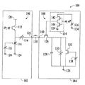
図1を参照すると、本発明の一実施形態による、集積回路(IC)デバイス102とICデバイス104とを有するマルチデバイスシステム100が図示してある。ICデバイス102,104は、半導体チップとすることができる。ICデバイス102は出力回路106を含み、その一方でICデバイス104は入力回路108を含み、この入力回路は出力回路から伝送される出力信号により駆動される。ICデバイス102,104は電気結線110によりインタフェースがとられており、この結線がICデバイス102の出力回路106とICデバイス104の入力回路108を接続している。電気結線110は、ボンディングワイヤ及び/又は短絡(λ≪λ/4)伝送線路とすることができる。図1に示した如く、電気結線110は誘導的であり、それが誘導性共振に起因するかなりのピーキングを招く。出力回路106と入力回路108は、ICデバイスのインタフェースによる電圧ピーキングが制御できるよう、それぞれのインピーダンスがICデバイス102,104の製造後に調整し得るように設計してある。
Referring to FIG. 1, there is illustrated a
ICデバイス102の出力回路106は、駆動トランジスタ112と随意選択的な調整可能抵抗器114と調整可能電流源116と調整可能電圧源118を含む。駆動トランジスタ112は、エミッターフォロワとして構成したバイポーラトランジスタである。かくして、駆動トランジスタ112のコレクタは高電圧端子(例えば、供給電圧端子)に接続され、トランジスタのエミッタは随意選択的な調整可能抵抗器114を介して出力ノード122に接続される。駆動トランジスタ112のエミッタはまた、調整可能電流源116に接続してある。他の実施形態では、駆動トランジスタ112は電界効果トランジスタ(FET)や相補型金属酸化膜半導体(CMOS)などの他種のトランジスタとすることもできる。出力ノード122は、電気結線110に接続してある。駆動トランジスタ112のベースは、駆動信号drv_sigを受信する構成としてあり、この信号が駆動トランジスタ112を通って流れる電流を制御(増大或いは減少)する。かくして、駆動信号は出力回路106から入力回路108へ伝送される出力信号を決定して入力回路を駆動する。
調整可能電流源116は、駆動トランジスタ112のエミッタと低電圧端子124、例えばグラウンドとの間に直列接続してある。調整可能電流源116は、調整可能電圧源118からの制御電圧により制御される。調整可能電流源116が引き込む電流は、制御電圧に依存する。かくして、調整可能電流源116が引き込む電流は調整可能電圧源118からの制御電圧を変化させることで調整することができる。従って、固定された電流源とは対照的に、調整可能電流源116が引き込む電流をICデバイス102の製作後に調整し、下記の如く伝送出力信号の電圧ピーキングを制御することができる。一例として、調整可能電流源116はバイポーラトランジスタとすることもでき、調整可能電圧源118はオン・デバイスのディジタル/アナログ(D/A)変換器とすることもできる。本例では、バイポーラトランジスタが引き込む電流はディジタル信号をD/A変換器に選択的に伝送することで制御され、これによりバイポーラ電流源トランジスタに対するアナログ制御電圧を調整することができる。別の例では、調整可能電圧源118は調整可能抵抗器付き分圧器とし、分圧器が供給する電圧が調整可能となるようにすることもできる。
An adjustable
出力回路106の随意選択的な調整可能抵抗器114は、駆動トランジスタ112のエミッタと出力ノード122との間に接続してあり、その抵抗値を製造後に調整することのできる抵抗器としてある。一例として、調整可能抵抗器114はレーザによりトリミングして抵抗器の抵抗値を変えることのできる抵抗器でよい。別の例では、調整可能抵抗器114は選択的に短絡させることのできる抵抗器群とし、幾つかの抵抗器だけを動作させて被接続抵抗器の総抵抗値を変えることができるようにすることもできる。
An optional
出力回路106の構成により、出力回路のインピーダンスはICデバイス102の製作後に調整できるようになっている。出力回路106のインピーダンスは調整可能電流源116が引き込む電流を変化させることで調整され、調整可能電流源116は調整可能電圧源118が調整可能電流源116に供給する制御電圧によって制御される。出力回路106のインピーダンスは、調整可能抵抗器114の抵抗を変えることでも調整することができる。出力回路106のインピーダンスがICデバイス102からICデバイス104へ伝送される出力信号の電圧ピーキングに影響を及ぼすので、電圧ピーキングは調整可能電流源116及び/又は調整可能抵抗器114を用いて出力回路のインピーダンスを選択的に調整することで少なくとも一部制御することができる。
The configuration of the
ICデバイス104の入力回路108は、パストランジスタ126と負荷キャパシタ128と随意選択的な調整可能抵抗器130と随意選択的な抵抗値調整可能トランジスタ132とスイッチング装置134と調整可能電圧源136,138を含む。パストランジスタ126は入力ノード140に接続してあり、そのノードは電気結線110に接続してある。かくして、入力回路108の入力ノード140は電気結線110を介して出力回路106の出力ノード122に接続される。本実施形態では、パストランジスタ126はFETである。しかしながら、パストランジスタは他種のトランジスタとすることもできる。パストランジスタ126は、トランジスタのゲートに供給される制御信号により選択的に作動されてICデバイス102の出力回路106から伝送される出力信号をサンプリングするサンプリングトランジスタとすることができる。パストランジスタ126のゲートに供給する制御信号の電圧をICデバイス104製造後に調整し、これによりパストランジスタのオン抵抗を変えることができる。パストランジスタ126のゲートへの制御信号はスイッチング装置134を介して調整可能電圧源136により供給され、この装置はサンプリング用クロック信号でよいオンオフ信号on_offに基づいて制御信号を選択的に伝送する構成としてある。本実施形態では、スイッチング装置134は相補型のPチャンネル金属酸化膜半導体(PMOS)トランジスタ142及びNチャンネル金属酸化膜半導体(NMOS)トランジスタ144を含む。PMOSトランジスタ142とNMOSトランジスタ144は、調整可能電圧源136と低電圧端子124との間に直列接続してある。PMOSトランジスタ142とNMOSトランジスタ144のゲートはオンオフ信号を受信するよう接続してあり、この信号が選択的にPMOSトランジスタを作動させ、NMOSトランジスタを作動停止させて、パストランジスタ126のゲートへ制御信号を伝送する。PMOSトランジスタの選択的な作動が調整可能電圧源136をパストランジスタ126のゲートへ接続するので、調整可能電圧源136が供給する電圧がパストランジスタのゲートの制御信号電圧を制御する。調整可能電圧源136は、オン・デバイスのディジタル/アナログ(D/A)変換器或いは調整可能抵抗器付き分圧器とすることができる。
The
入力回路108の負荷キャパシタ128は、パストランジスタ126と低電圧端子124との間に接続してある。負荷キャパシタ128は、寄生回路容量及び/又は故意に付加した容量を表わすことができる。随意選択的な調整可能抵抗器130は、負荷キャパシタ128に並列接続してある。出力回路106の調整可能抵抗器114と同様、調整可能抵抗器130の抵抗値はICデバイス104の製作後に調整することができる。調整可能抵抗器130は、レーザによるトリミングが可能な抵抗器などの製造後に抵抗値を調整することのできるどんな種類の抵抗器であってもよい。随意選択的な抵抗値調整可能トランジスタ132もまた、負荷キャパシタ128に並列接続される。本実施形態では、抵抗値調整可能トランジスタ132はFETである。しかしながら、抵抗値調整可能トランジスタは他種のトランジスタとすることもできる。抵抗値調整可能トランジスタ132は、調整可能抵抗器として機能する線形領域で動作する。抵抗値調整可能トランジスタ132のゲートは調整可能電圧源138に接続してあり、この電圧源はオン・デバイスのD/A変換器或いは調整可能抵抗器付き分圧器とすることができる。調整可能電圧源138はICデバイス104の製造後に調整することのできる電圧を抵抗値調整可能トランジスタ132のゲートへ供給し、トランジスタのオン抵抗を調整する。抵抗値調整可能トランジスタを調整可能抵抗器として動作させるため、ドレイン・ソース間電圧(Vds)はゲート・ソース間電圧と閾値電圧との差分(Vgs−Vth)未満としなければならない。代替構成では、調整可能抵抗器130及び/又は抵抗値調整可能トランジスタ132は入力ノード140と低電圧端子124との間に並列に直接接続することができる。
The
入力回路108の構成により、ICデバイス104の製造後に入力回路のインピーダンスを調整することができる。例えば、入力回路108のインピーダンスは調整可能電圧源136の電圧を調整してパストランジスタ126に供給される制御信号の電圧を調整することで先ず調整することができる。入力回路108のインピーダンスは次に、調整可能電圧源138から抵抗値調整可能トランジスタ132に供給される電圧を調整することで調整することができる。入力回路108のインピーダンスは次に、調整可能抵抗器130の抵抗値を変えることにより更に調整することができる。パストランジスタ126に供給される制御電圧、抵抗値調整可能トランジスタ132に供給される電圧、および調整可能抵抗器130の抵抗値に対し他の手順の調整を施して、入力回路108のインピーダンスを調整することができる。入力回路のインピーダンスがICデバイス102からICデバイス104へ伝送される出力信号の電圧ピーキングに影響を及ぼすため、パストランジスタ126と調整可能抵抗器130及び/又は抵抗値調整可能トランジスタ132を用いて入力回路108のインピーダンスを選択的に調整することで電圧ピーキングを少なくとも一部制御することができる。
With the configuration of the
ここで図2を参照すると、本発明の別の実施形態による、ICデバイス202とICデバイス204とを有するマルチデバイスシステム200が図示してある。図2のマルチデバイスシステム200は、図1のマルチデバイスシステム100の差動版である。かくして、本実施形態では、ICデバイス202はICデバイス204の入力回路208に差動信号を伝送して入力回路を駆動するよう設計された出力回路206を含む。図1のマルチデバイスシステム100と同様、入力回路208と出力回路206は、ICデバイス202,204の製造後に入力回路及び/又は出力回路のインピーダンスを調整して差動信号の電圧ピーキングを制御できるよう構成してある。
Referring now to FIG. 2, a
ICデバイス202の出力回路206は、駆動トランジスタ210と随意選択的な調整可能抵抗器212と調整可能電流源214と調整可能電圧源216とを含む。これらの構成要素は、図1のマルチデバイスシステム100の出力回路106と同一構成において、高電圧端子218と低電圧端子220(例えば、グラウンド)と出力ノード222とに接続してある。出力回路206には更に、駆動トランジスタ224と随意選択的な調整可能抵抗器226と調整可能電流源228と調整可能電圧源230とが含まれ、それらは同様に高電圧端子218と低電圧端子220と出力ノード232とに接続してある。他の実施形態では、調整可能電圧源216,230は調整可能電流源214,228の双方に制御電圧を供給する単一の調整可能電圧源により置き換えることもできる。
The
駆動トランジスタ210,224は駆動信号drv_sig,バーdrv_sigを受信し、この駆動信号が出力ノード222,232を介してICデバイス204の入力回路208へ駆動トランジスタを交互に通って流れる電流を制御(増大し減少させる)する。出力ノード222,232は電気結線234,236に接続してあり、それらの結線がICデバイス202の出力回路206とICデバイス204の入力回路208を接続している。電気結線234,236は、ボンディングワイヤ及び/又は短絡(λ≪λ/4)伝送線路とすることができる。
The
図1のマルチデバイスシステム100の出力回路106と同様、出力回路206の構成により出力回路206のインピーダンスはICデバイス202の製造後に調整できるようになる。かくして、出力回路206から入力回路208へ伝送される差動信号の電圧ピーキングは、調整可能電流源214,228及び/又は随意選択的な調整可能抵抗器212,226を用いて出力回路206のインピーダンスを調整することにより少なくとも部分的に制御することができる。
Like the
ICデバイス204の入力回路208には、パストランジスタ238と負荷キャパシタ240とスイッチング装置242と調整可能電圧源244とが含まれる。これらの構成要素は、図1のマルチデバイスシステム100の入力回路108と同じ構成において入力ノード246と低電圧端子220との間に直列に接続してある。入力ノード246は、電気結線234に接続してある。かくして、入力ノード246は出力回路206の出力ノード222に電気的に接続され、出力回路が伝送する差動信号の一方を受信する。入力回路208は更に、パストランジスタ248と負荷キャパシタ250とスイッチング装置252と調整可能電圧源254とを含み、それらは同様に入力ノード256と低電圧端子220との間に直列に接続してある。入力ノード256は、電気結線236へ接続してある。かくして、入力ノード256は出力回路206の出力ノード232に電気的に接続され、出力回路により伝送される差動信号の他方を受信する。スイッチング装置242,252は、サンプリング用クロック信号でよいオンオフ信号on_offを受信する構成としてある。オンオフ信号はスイッチング装置を選択的に作動或いは作動停止させ、サンプリングトランジスタでよいパストランジスタ238,248へ調整可能電圧源244,254により供給される電圧に基づいた制御信号を伝送する。例示実施形態では、各スイッチング装置は相補型のPMOSトランジスタ258とNMOSトランジスタ260を含み、それらは個々の調整可能電圧源244や254と低電圧端子220とに直列接続してある。PMOSトランジスタ258とNMOSトランジスタ260のゲートはオンオフ信号を受信するよう構成してあり、このオンオフ信号が選択的にPMOSトランジスタ258を作動させるとともにNMOSトランジスタ260を作動停止させ、それにより、制御信号の一つが個々のパストランジスタ238,248のゲートへ伝送される。制御信号がパストランジスタ238,248を選択的に作動させ、例えば出力回路206からの差動信号をサンプリングする。
The
入力回路208は更に、随意選択的な調整可能抵抗器262と随意選択的な抵抗値調整可能トランジスタ264とを含み、それらはパストランジスタ238,248間に並列に接続してある。抵抗値調整可能トランジスタ264は、調整可能電圧源266へも接続してある。調整可能電圧源266は、抵抗値調整可能トランジスタ264へ制御電圧を供給する。抵抗値調整可能トランジスタ264は線形領域で動作して調整可能抵抗器として機能し、その抵抗値は調整可能電圧源からの制御電圧を調整することで変化させることができる。調整可能抵抗器262は、ICデバイス204の製造後に抵抗値を調整することのできる抵抗器である。代替構成では、調整可能抵抗器262及び/又は抵抗値調整可能トランジスタ264を入力ノード246と256との間に並列に直接接続することもできる。
図1のマルチデバイスシステム100の入力回路108と同様、入力回路208の構成によってICデバイス204の製作後に入力回路208のインピーダンスが調整できるようにしてある。かくして、ICデバイス202の出力回路から伝送される差動信号の電圧ピーキングは、パストランジスタ238,248と随意選択的な抵抗器262及び/又は随意選択的な抵抗値調整可能トランジスタ264を用いて入力回路208のインピーダンスを調整することで少なくとも一部制御することができる。
Like the
マルチデバイスシステム100,200の出力回路106,206の調整可能電流源116,214,228が調整可能電圧により制御されるものとして説明したが、これらの調整可能電流源は代わって調整可能電流により制御することもできる。同様に、パストランジスタ126,238,248と抵抗値調整可能トランジスタ132,264は、調整可能電圧ではなく調整可能電流によって制御することもできる。
Although the adjustable
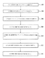
本発明の一実施形態に従いICデバイス間で伝送される出力信号の電圧ピーキング制御方法を、図3のフロー線図を参照して説明する。ブロック302において、出力回路を有する第1のICデバイスが設けられる。一例として、出力回路は図1のマルチデバイスシステム100の出力回路や図2のマルチデバイスシステム200の出力回路206とすることができる。ブロック304において、入力回路を有する第2のICデバイスが設けられる。一例として、入力回路は図1のマルチデバイスシステム100の入力回路108や図2のマルチデバイスシステム200の入力回路208とすることができる。ブロック306において、入力回路のパストランジスタに印加される制御信号を調整し、パストランジスタのオン抵抗を変える。随意選択的なブロック308において、パストランジスタと低電圧端子との間に直列接続した入力回路の調整可能抵抗器の抵抗値を変える。随意選択的なブロック310において、パストランジスタと低電圧端子との間に直列接続した入力回路の抵抗値調整可能トランジスタに印加する制御信号を調整し、トランジスタのオン抵抗を調整する。随意選択的なブロック312において、高電圧端子と低電圧端子の間に駆動トランジスタと直列に接続した出力回路の調整可能電流源に供給される制御信号を調整し、調整可能電流源が引き込む電流を調整する。随意選択的なブロック314において、駆動トランジスタと出力ノードとの間に直列に接続した出力回路の調整可能抵抗器の抵抗値を変える。ブロック306乃至314の実行により、入力回路及び/又は出力回路のインピーダンスを調整し、そのことで出力回路から入力回路へ伝送される出力信号の電圧ピーキングに影響を与える。かくして、出力信号の電圧ピーキングは、ブロック306〜314の1つ以上を実行することで制御することができる。
A method of controlling voltage peaking of an output signal transmitted between IC devices according to an embodiment of the present invention will be described with reference to the flowchart of FIG. At
本発明の特定の実施形態を説明し図示してきたが、本発明はかく説明し図示した部品の特定の形態や配置に限定すべきではない。本発明範囲は、本願明細書に添付した特許請求の範囲とそれらの等価物により規定される。 While particular embodiments of the present invention have been described and illustrated, the invention should not be limited to the particular forms or arrangements of components thus described and illustrated. The scope of the invention is defined by the claims appended hereto and their equivalents.
100:マルチデバイスシステム
102,104:集積回路デバイス
106:出力回路
108:入力回路
110:電気結線
112:駆動トランジスタ
114,130:調整可能抵抗器
116:調整可能電流源
118,136,138:調整可能電圧源
120:高電圧端子
122:出力ノード
124:低電圧端子
126:パストランジスタ
128:負荷キャパシタ
132:抵抗値調整可能トランジスタ
134:スイッチング装置
140:入力ノード
142:PMOSトランジスタ
144:NMOSトランジスタ
100:
Claims (10)
前記入力回路を配設するステップであって、該入力回路は、入力ノードと低電圧端子との間に直列接続されたパストランジスタを有し、前記入力ノードは、前記出力回路から前記出力信号を受信するように接続されている、ステップと、
前記入力回路の前記パストランジスタに印加される制御信号を調整して該パストランジスタのオン抵抗を変えるステップであって、前記パストランジスタの前記オン抵抗は、前記電圧ピーキングが、前記パストランジスタの前記オン抵抗の変化により少なくとも部分的に制御され得るように、前記出力信号の前記電圧ピーキングと所定の関係を有している、ステップと、
を含む方法。 A method for controlling voltage peaking of an output signal transmitted from an output circuit to an input circuit,
Arranging the input circuit, the input circuit having a pass transistor connected in series between an input node and a low voltage terminal, wherein the input node receives the output signal from the output circuit. A step, connected to receive;
Adjusting the control signal applied to the pass transistor of the input circuit to change the on-resistance of the pass transistor, wherein the on-resistance of the pass transistor is such that the voltage peaking is caused by the on-state of the pass transistor. Having a predetermined relationship with the voltage peaking of the output signal such that it can be at least partially controlled by a change in resistance;
A method that includes
前記出力回路の前記調整可能抵抗器の抵抗値を変えるステップと、
を更に含む、請求項1乃至3のいずれか1項に記載の方法。 Providing the output circuit having a drive transistor connected in series between a high voltage terminal and a low voltage terminal, the output circuit being connected in series between the drive transistor and an output node. Also having an adjustable resistor, wherein the output node is electrically connected to the input node of the input circuit for transmitting the output signal to the input circuit;
Changing the resistance of the adjustable resistor of the output circuit;
The method according to any one of claims 1 to 3, further comprising:
前記出力回路の調整可能電流源へ供給される制御信号電圧を調整して、前記調整可能電流源によって引き込まれる電流を変えるステップと、
を更に含む、請求項1乃至4のいずれか1項に記載の方法。 Arranging the output circuit, the output circuit including a driving transistor and an adjustable current source connected in series between a high voltage terminal and a low voltage terminal, wherein the output circuit includes the driving circuit. An output node connected to a transistor, wherein the output node is electrically connected to the input node of the input circuit to transmit the output signal to the input circuit;
Adjusting a control signal voltage supplied to an adjustable current source of the output circuit to change a current drawn by the adjustable current source;
The method according to any one of claims 1 to 4, further comprising:
前記出力回路に電気的に接続された入力回路を有する第2の集積回路デバイスであって、前記入力回路が、
前記出力回路に接続されて前記出力信号を受信する入力ノードと、
前記入力ノードに接続されたパストランジスタであって、制御信号を受信して前記パストランジスタを選択的に作動させる制御電極を有する前記パストランジスタと、
前記パストランジスタの前記制御電極に直列接続された調整可能信号源であって、前記制御信号を調整して前記パストランジスタのオン抵抗を変え、それにより、前記出力信号の電圧ピーキングを制御する前記調整可能信号源と、
を有する前記第2の集積回路デバイスと、
を備えているマルチデバイスシステム。 A first integrated circuit device having an output circuit configured to transmit an output signal;
A second integrated circuit device having an input circuit electrically connected to the output circuit, wherein the input circuit comprises:
An input node connected to the output circuit for receiving the output signal;
A pass transistor connected to the input node, the pass transistor having a control electrode for receiving a control signal and selectively operating the pass transistor;
An adjustable signal source serially connected to the control electrode of the pass transistor, wherein the adjustable signal source adjusts the control signal to change the on-resistance of the pass transistor, thereby controlling voltage peaking of the output signal. Possible signal sources,
The second integrated circuit device having:
A multi-device system comprising:
The input circuit further comprises a resistance-adjustable transistor connected in series to the input node, wherein the resistance-adjustable transistor supplies a second control signal to the resistance-adjustable transistor. 7. The second adjustable signal source also connected to a signal source, wherein the second adjustable signal source is configured such that the second control signal can be adjusted to change the on-resistance of the resistance adjustable transistor. 10. The multi-device system according to any one of claims 9 to 9.
Applications Claiming Priority (1)
| Application Number | Priority Date | Filing Date | Title |
|---|---|---|---|
| US10/354,400 US6956402B2 (en) | 2003-01-30 | 2003-01-30 | Multi-device system and method for controlling voltage peaking of an output signal transmitted between integrated circuit devices |
Publications (2)
| Publication Number | Publication Date |
|---|---|
| JP2004236311A true JP2004236311A (en) | 2004-08-19 |
| JP2004236311A5 JP2004236311A5 (en) | 2007-03-08 |
Family
ID=32655545
Family Applications (1)
| Application Number | Title | Priority Date | Filing Date |
|---|---|---|---|
| JP2004012760A Pending JP2004236311A (en) | 2003-01-30 | 2004-01-21 | Multi-device system and method for controlling voltage peaking of output signal transmitted between integrated circuit devices |
Country Status (3)
| Country | Link |
|---|---|
| US (1) | US6956402B2 (en) |
| EP (1) | EP1443651A1 (en) |
| JP (1) | JP2004236311A (en) |
Cited By (1)
| Publication number | Priority date | Publication date | Assignee | Title |
|---|---|---|---|---|
| JP2006303668A (en) * | 2005-04-18 | 2006-11-02 | Matsushita Electric Ind Co Ltd | Output impedance variable circuit |
Families Citing this family (3)
| Publication number | Priority date | Publication date | Assignee | Title |
|---|---|---|---|---|
| JP4652703B2 (en) * | 2004-03-10 | 2011-03-16 | ルネサスエレクトロニクス株式会社 | Semiconductor circuit device and multi-chip package |
| KR100773746B1 (en) * | 2006-01-31 | 2007-11-09 | 삼성전자주식회사 | Device for adjusting transmit signal level based on channel loading |
| KR102573219B1 (en) | 2018-09-14 | 2023-09-01 | 삼성전자주식회사 | An integrated circuit capable of controlling impedance and an electronic device comprising thereof |
Citations (1)
| Publication number | Priority date | Publication date | Assignee | Title |
|---|---|---|---|---|
| JP2003008419A (en) * | 2001-06-25 | 2003-01-10 | Nec Corp | Output impedance matching system for semiconductor ic |
Family Cites Families (8)
| Publication number | Priority date | Publication date | Assignee | Title |
|---|---|---|---|---|
| US4016481A (en) | 1975-11-26 | 1977-04-05 | Gte Automatic Electric Laboratories Incorporated | Unmatched field effect transistors providing matched voltage-controlled resistances |
| DE2950584C2 (en) * | 1979-12-15 | 1984-07-12 | Robert Bosch Gmbh, 7000 Stuttgart | Circuit arrangement with controllable resistance |
| US4390851A (en) * | 1980-11-25 | 1983-06-28 | Rockwell International Corporation | Monolithic microwave amplifier having active impedance matching |
| US4813045A (en) * | 1986-07-28 | 1989-03-14 | Tektronix, Inc. | Laser driver |
| US5852540A (en) * | 1997-09-24 | 1998-12-22 | Intel Corporation | Circuit for protecting the input/output stage of a low voltage integrated circuit device from a failure of the internal voltage supply or a difference in the power-up sequencing of supply voltage levels |
| US6198309B1 (en) | 1999-03-31 | 2001-03-06 | Applied Micro Circuits Corporation | Emitter follower output with programmable current |
| US6114876A (en) * | 1999-05-20 | 2000-09-05 | Pericom Semiconductor Corp. | Translator switch transistor with output voltage adjusted to match a reference by controlling gate and substrate charge pumps |
| US6781415B2 (en) * | 2001-11-27 | 2004-08-24 | Fairchild Semiconductor Corporation | Active voltage level bus switch (or pass gate) translator |
-
2003
- 2003-01-30 US US10/354,400 patent/US6956402B2/en not_active Expired - Fee Related
- 2003-09-18 EP EP03021205A patent/EP1443651A1/en not_active Withdrawn
-
2004
- 2004-01-21 JP JP2004012760A patent/JP2004236311A/en active Pending
Patent Citations (1)
| Publication number | Priority date | Publication date | Assignee | Title |
|---|---|---|---|---|
| JP2003008419A (en) * | 2001-06-25 | 2003-01-10 | Nec Corp | Output impedance matching system for semiconductor ic |
Cited By (1)
| Publication number | Priority date | Publication date | Assignee | Title |
|---|---|---|---|---|
| JP2006303668A (en) * | 2005-04-18 | 2006-11-02 | Matsushita Electric Ind Co Ltd | Output impedance variable circuit |
Also Published As
| Publication number | Publication date |
|---|---|
| US20040150424A1 (en) | 2004-08-05 |
| EP1443651A1 (en) | 2004-08-04 |
| US6956402B2 (en) | 2005-10-18 |
Similar Documents
| Publication | Publication Date | Title |
|---|---|---|
| US9225326B2 (en) | Voltage controlled switching element gate drive circuit | |
| US6771097B1 (en) | Series terminated CMOS output driver with impedance calibration | |
| US6236239B1 (en) | Output buffer circuit achieving stable operation and cost reduction | |
| JP4059387B2 (en) | Apparatus for changing the slew rate of a transition edge of a digital signal at a node of an integrated circuit | |
| US20040207451A1 (en) | Impedance trimming circuit | |
| US7683600B2 (en) | Output circuit | |
| TW200929859A (en) | High-swing operational amplifier output stage using adaptive biasing | |
| JP2002524957A (en) | Constant gate drive MOS analog switch | |
| US6664814B1 (en) | Output driver for an integrated circuit | |
| US7071739B1 (en) | Termination sense-and-match differential driver | |
| EP0357366A1 (en) | Improved current mirror circuit | |
| US7518424B2 (en) | Slew rate controlled output circuit | |
| US6400177B1 (en) | Output driver and method for meeting specified output impedance and current characteristics | |
| US7336119B2 (en) | Gate driver output stage with bias circuit for high and wide operating voltage range | |
| JP2004236311A (en) | Multi-device system and method for controlling voltage peaking of output signal transmitted between integrated circuit devices | |
| US7586357B2 (en) | Systems for providing a constant resistance | |
| US6181190B1 (en) | Electronic circuit and manufacturing method for electronic circuit | |
| US20230396260A1 (en) | Dac with configurable output stage | |
| US6825718B2 (en) | Impedance matching circuit | |
| US9577628B2 (en) | Gate pulsing gate ladder | |
| US6700419B1 (en) | Driving circuit for high frequency signal | |
| US7853008B2 (en) | Supply circuit for supplying a two-wire line | |
| CN116134789A (en) | Method and device for damping oscillations on bus lines of a bus system based on differential voltage signals | |
| CN115552852A (en) | Transmitting stage and method for generating a voltage difference between bus lines | |
| KR101469501B1 (en) | Tuning capacitor array |
Legal Events
| Date | Code | Title | Description |
|---|---|---|---|
| A521 | Written amendment |
Free format text: JAPANESE INTERMEDIATE CODE: A523 Effective date: 20070119 |
|
| A621 | Written request for application examination |
Free format text: JAPANESE INTERMEDIATE CODE: A621 Effective date: 20070119 |
|
| A977 | Report on retrieval |
Free format text: JAPANESE INTERMEDIATE CODE: A971007 Effective date: 20090916 |
|
| A131 | Notification of reasons for refusal |
Free format text: JAPANESE INTERMEDIATE CODE: A131 Effective date: 20091009 |
|
| A02 | Decision of refusal |
Free format text: JAPANESE INTERMEDIATE CODE: A02 Effective date: 20100402 |