JP2004235628A - InP-BASED HIGH-TEMPERATURE LASER HAVING InAsP QUANTUM WELL LAYER AND Gax(AlIn) l-xP BARRIER LAYER - Google Patents
InP-BASED HIGH-TEMPERATURE LASER HAVING InAsP QUANTUM WELL LAYER AND Gax(AlIn) l-xP BARRIER LAYER Download PDFInfo
- Publication number
- JP2004235628A JP2004235628A JP2004007511A JP2004007511A JP2004235628A JP 2004235628 A JP2004235628 A JP 2004235628A JP 2004007511 A JP2004007511 A JP 2004007511A JP 2004007511 A JP2004007511 A JP 2004007511A JP 2004235628 A JP2004235628 A JP 2004235628A
- Authority
- JP
- Japan
- Prior art keywords
- layer
- quantum well
- barrier layer
- inasp
- barrier
- Prior art date
- Legal status (The legal status is an assumption and is not a legal conclusion. Google has not performed a legal analysis and makes no representation as to the accuracy of the status listed.)
- Withdrawn
Links
Images


Classifications
-
- B—PERFORMING OPERATIONS; TRANSPORTING
- B82—NANOTECHNOLOGY
- B82Y—SPECIFIC USES OR APPLICATIONS OF NANOSTRUCTURES; MEASUREMENT OR ANALYSIS OF NANOSTRUCTURES; MANUFACTURE OR TREATMENT OF NANOSTRUCTURES
- B82Y20/00—Nanooptics, e.g. quantum optics or photonic crystals
-
- H—ELECTRICITY
- H01—ELECTRIC ELEMENTS
- H01S—DEVICES USING THE PROCESS OF LIGHT AMPLIFICATION BY STIMULATED EMISSION OF RADIATION [LASER] TO AMPLIFY OR GENERATE LIGHT; DEVICES USING STIMULATED EMISSION OF ELECTROMAGNETIC RADIATION IN WAVE RANGES OTHER THAN OPTICAL
- H01S5/00—Semiconductor lasers
- H01S5/30—Structure or shape of the active region; Materials used for the active region
- H01S5/34—Structure or shape of the active region; Materials used for the active region comprising quantum well or superlattice structures, e.g. single quantum well [SQW] lasers, multiple quantum well [MQW] lasers or graded index separate confinement heterostructure [GRINSCH] lasers
- H01S5/343—Structure or shape of the active region; Materials used for the active region comprising quantum well or superlattice structures, e.g. single quantum well [SQW] lasers, multiple quantum well [MQW] lasers or graded index separate confinement heterostructure [GRINSCH] lasers in AIIIBV compounds, e.g. AlGaAs-laser, InP-based laser
- H01S5/3434—Structure or shape of the active region; Materials used for the active region comprising quantum well or superlattice structures, e.g. single quantum well [SQW] lasers, multiple quantum well [MQW] lasers or graded index separate confinement heterostructure [GRINSCH] lasers in AIIIBV compounds, e.g. AlGaAs-laser, InP-based laser with a well layer comprising at least both As and P as V-compounds
-
- H—ELECTRICITY
- H01—ELECTRIC ELEMENTS
- H01S—DEVICES USING THE PROCESS OF LIGHT AMPLIFICATION BY STIMULATED EMISSION OF RADIATION [LASER] TO AMPLIFY OR GENERATE LIGHT; DEVICES USING STIMULATED EMISSION OF ELECTROMAGNETIC RADIATION IN WAVE RANGES OTHER THAN OPTICAL
- H01S2302/00—Amplification / lasing wavelength
-
- H—ELECTRICITY
- H01—ELECTRIC ELEMENTS
- H01S—DEVICES USING THE PROCESS OF LIGHT AMPLIFICATION BY STIMULATED EMISSION OF RADIATION [LASER] TO AMPLIFY OR GENERATE LIGHT; DEVICES USING STIMULATED EMISSION OF ELECTROMAGNETIC RADIATION IN WAVE RANGES OTHER THAN OPTICAL
- H01S5/00—Semiconductor lasers
- H01S5/30—Structure or shape of the active region; Materials used for the active region
- H01S5/34—Structure or shape of the active region; Materials used for the active region comprising quantum well or superlattice structures, e.g. single quantum well [SQW] lasers, multiple quantum well [MQW] lasers or graded index separate confinement heterostructure [GRINSCH] lasers
- H01S5/3403—Structure or shape of the active region; Materials used for the active region comprising quantum well or superlattice structures, e.g. single quantum well [SQW] lasers, multiple quantum well [MQW] lasers or graded index separate confinement heterostructure [GRINSCH] lasers having a strained layer structure in which the strain performs a special function, e.g. general strain effects, strain versus polarisation
- H01S5/3406—Structure or shape of the active region; Materials used for the active region comprising quantum well or superlattice structures, e.g. single quantum well [SQW] lasers, multiple quantum well [MQW] lasers or graded index separate confinement heterostructure [GRINSCH] lasers having a strained layer structure in which the strain performs a special function, e.g. general strain effects, strain versus polarisation including strain compensation
-
- H—ELECTRICITY
- H01—ELECTRIC ELEMENTS
- H01S—DEVICES USING THE PROCESS OF LIGHT AMPLIFICATION BY STIMULATED EMISSION OF RADIATION [LASER] TO AMPLIFY OR GENERATE LIGHT; DEVICES USING STIMULATED EMISSION OF ELECTROMAGNETIC RADIATION IN WAVE RANGES OTHER THAN OPTICAL
- H01S5/00—Semiconductor lasers
- H01S5/30—Structure or shape of the active region; Materials used for the active region
- H01S5/34—Structure or shape of the active region; Materials used for the active region comprising quantum well or superlattice structures, e.g. single quantum well [SQW] lasers, multiple quantum well [MQW] lasers or graded index separate confinement heterostructure [GRINSCH] lasers
- H01S5/3407—Structure or shape of the active region; Materials used for the active region comprising quantum well or superlattice structures, e.g. single quantum well [SQW] lasers, multiple quantum well [MQW] lasers or graded index separate confinement heterostructure [GRINSCH] lasers characterised by special barrier layers
-
- H—ELECTRICITY
- H01—ELECTRIC ELEMENTS
- H01S—DEVICES USING THE PROCESS OF LIGHT AMPLIFICATION BY STIMULATED EMISSION OF RADIATION [LASER] TO AMPLIFY OR GENERATE LIGHT; DEVICES USING STIMULATED EMISSION OF ELECTROMAGNETIC RADIATION IN WAVE RANGES OTHER THAN OPTICAL
- H01S5/00—Semiconductor lasers
- H01S5/30—Structure or shape of the active region; Materials used for the active region
- H01S5/34—Structure or shape of the active region; Materials used for the active region comprising quantum well or superlattice structures, e.g. single quantum well [SQW] lasers, multiple quantum well [MQW] lasers or graded index separate confinement heterostructure [GRINSCH] lasers
- H01S5/343—Structure or shape of the active region; Materials used for the active region comprising quantum well or superlattice structures, e.g. single quantum well [SQW] lasers, multiple quantum well [MQW] lasers or graded index separate confinement heterostructure [GRINSCH] lasers in AIIIBV compounds, e.g. AlGaAs-laser, InP-based laser
- H01S5/34306—Structure or shape of the active region; Materials used for the active region comprising quantum well or superlattice structures, e.g. single quantum well [SQW] lasers, multiple quantum well [MQW] lasers or graded index separate confinement heterostructure [GRINSCH] lasers in AIIIBV compounds, e.g. AlGaAs-laser, InP-based laser emitting light at a wavelength longer than 1000nm, e.g. InP based 1300 and 1500nm lasers
-
- H—ELECTRICITY
- H01—ELECTRIC ELEMENTS
- H01S—DEVICES USING THE PROCESS OF LIGHT AMPLIFICATION BY STIMULATED EMISSION OF RADIATION [LASER] TO AMPLIFY OR GENERATE LIGHT; DEVICES USING STIMULATED EMISSION OF ELECTROMAGNETIC RADIATION IN WAVE RANGES OTHER THAN OPTICAL
- H01S5/00—Semiconductor lasers
- H01S5/30—Structure or shape of the active region; Materials used for the active region
- H01S5/34—Structure or shape of the active region; Materials used for the active region comprising quantum well or superlattice structures, e.g. single quantum well [SQW] lasers, multiple quantum well [MQW] lasers or graded index separate confinement heterostructure [GRINSCH] lasers
- H01S5/343—Structure or shape of the active region; Materials used for the active region comprising quantum well or superlattice structures, e.g. single quantum well [SQW] lasers, multiple quantum well [MQW] lasers or graded index separate confinement heterostructure [GRINSCH] lasers in AIIIBV compounds, e.g. AlGaAs-laser, InP-based laser
- H01S5/34346—Structure or shape of the active region; Materials used for the active region comprising quantum well or superlattice structures, e.g. single quantum well [SQW] lasers, multiple quantum well [MQW] lasers or graded index separate confinement heterostructure [GRINSCH] lasers in AIIIBV compounds, e.g. AlGaAs-laser, InP-based laser characterised by the materials of the barrier layers
- H01S5/3436—Structure or shape of the active region; Materials used for the active region comprising quantum well or superlattice structures, e.g. single quantum well [SQW] lasers, multiple quantum well [MQW] lasers or graded index separate confinement heterostructure [GRINSCH] lasers in AIIIBV compounds, e.g. AlGaAs-laser, InP-based laser characterised by the materials of the barrier layers based on InGa(Al)P
Abstract
Description
本発明は概して発光素子に関し、詳しくは半導体レーザーに関する。 The present invention relates generally to light emitting devices, and more particularly to semiconductor lasers.
波長1.3μmで動作する半導体レーザーの主な製造方法では、InP基板上に形成され複数のInAsP歪み量子井戸が用いられる。いずれの半導体レーザーにとっても、デバイスの性能を決定する要因の1つは閾値電流が受ける温度の影響である。 In a main method of manufacturing a semiconductor laser operating at a wavelength of 1.3 μm, a plurality of strained InAsP quantum wells formed on an InP substrate are used. For any semiconductor laser, one of the factors that determines device performance is the temperature effect on the threshold current.
InP基板上に設けられた従来のレーザーの閾値電流および放射効率は、動作温度に強く依存する。具体的には、閾値電流Ithは次の式で定義される。 The threshold current and emission efficiency of a conventional laser provided on an InP substrate strongly depend on the operating temperature. Specifically, the threshold current I th is defined by the following equation.
Ith=IOexp(T/TO) (式1) I th = I O exp (T / T O ) (Equation 1)
ただし、IOは定数、Tは動作温度、TOは特性温度である。式1に示すように、閾値電流Ithは温度比T/TOが増大するのにつれて指数関数的に増大する。従って、TOを非常に大きな値にすれば、閾値電流Ithは温度Tの変化の影響をほとんど受けなくなる。従って、優れた高温特性をレーザーで実現するためには、特性温度TOを大きくすることより、温度の影響を受けにくい特性にすることが望ましい。 Here, I O is a constant, T is an operating temperature, and T O is a characteristic temperature. As shown in Equation 1, the threshold current I th increases exponentially as the temperature ratio T / T O increases. Therefore, if T O is set to a very large value, the threshold current I th is hardly affected by the change in the temperature T. Therefore, in order to realize excellent high-temperature characteristics with a laser, it is desirable to make the characteristics less affected by temperature by increasing the characteristic temperature T O.
従来のInAsP活性領域の場合、量子井戸層のInAsPと障壁層の物質との間の伝導帯バンドオフセットが小さいことが原因で電子閉じ込め能力が低いため、温度性能に制約がある。従ってそれらのレーザーの高温時の性能は満足できるものではない。 In the case of the conventional InAsP active region, the electron confinement ability is low due to a small conduction band offset between the InAsP of the quantum well layer and the material of the barrier layer, so that the temperature performance is limited. Therefore, the performance of these lasers at high temperatures is not satisfactory.
例えば、活性領域がInAsPである場合、障壁層物質として用いられる一般的な物質を2つをあげると、InGaPとAlInGaAsがあげられる。InAsP量子井戸層とInGaP障壁層とを有するレーザーは閾値電流が小さいが、これらのレーザーは温度が高くなると劣悪な性能しか示さない。InAsPとInGaPとの間の伝導帯の不連続性に関しては、科学界においてかなり大きな意見の相違がある点に注意する必要がある。 For example, when the active region is InAsP, two common materials used as barrier layer materials include InGaP and AlInGaAs. Lasers with InAsP quantum well layers and InGaP barrier layers have low threshold currents, but these lasers show poor performance at higher temperatures. It should be noted that there is considerable disagreement in the scientific community regarding the conduction band discontinuity between InAsP and InGaP.
InAsP量子井戸層とAlInGaAs障壁層とを有するレーザーは、InAsP量子井戸層とInGaP障壁層とを有するレーザーよりも閾値電流が大きいが、高温での特性は優れている。その理由は、InAsP/AlInGaAs界面における欠陥の存在である。例えば、それらの欠陥は、量子井戸層または障壁層において無放射部の中心として作用し、閾値電流を増大させ、TOを大きくする場合がある。 A laser having an InAsP quantum well layer and an AlInGaAs barrier layer has a larger threshold current than a laser having an InAsP quantum well layer and an InGaP barrier layer, but has excellent characteristics at high temperatures. The reason is the presence of defects at the InAsP / AlInGaAs interface. For example, these defects may act as centers of non-radiative portions in the quantum well or barrier layers, increasing the threshold current and increasing T O.
また、エピタキシャル成長によって形成されるInAsPの層の品質は、一般に成膜温度が低くなるほど向上する。従って、InAsP量子井戸層を有する活性領域は、比較的低温度で形成される。しかしながら、障壁層物質AlInGaAsの結晶品質を向上させるためには高い成膜温度が必要であり、低い成膜温度では、量子井戸層物質InAsPの上に高品質のAlInGaAs障壁層を作成することが出来ない。 In addition, the quality of an InAsP layer formed by epitaxial growth generally improves as the film formation temperature decreases. Therefore, the active region having the InAsP quantum well layer is formed at a relatively low temperature. However, in order to improve the crystal quality of the barrier layer material AlInGaAs, a high film formation temperature is required. At a low film formation temperature, a high quality AlInGaAs barrier layer can be formed on the quantum well layer material InAsP. Absent.
従って、量子井戸層がInAsPである場合、障壁層物質にInGaPやAlInGaAsを使用しても、所望の低い閾値電流や、高温でのレーザー性能を得ることは出来ない。そのため、上述のような欠点を解決したいという産業上の需要がある。 Therefore, when the quantum well layer is made of InAsP, even if InGaP or AlInGaAs is used as the barrier layer material, a desired low threshold current and high-temperature laser performance cannot be obtained. Therefore, there is an industrial demand to solve the above-mentioned disadvantages.
本発明は、高温において波長1.3μmで動作するレーザー構造と、そのようなレーザー構造を製造する方法を提供する。このレーザー構造はInAsPの量子井戸層を含む。量子井戸層は第1の障壁層と第2の障壁層の間に挟まれる。各障壁層の物質は、量子井戸層の物質よりも高いバンドギャップエネルギーを有する。各障壁層は、Gax(AlIn)1-xPを含む。ただしx=0である。この物質は、InGaP等の従来の障壁層物質よりも高いバンドギャップエネルギーを有する。そのため、伝導帯の不連続性が大きくなり、レーザー構造の閾値電流を増大させることなく高温での性能を向上させることができる。 The present invention provides a laser structure operating at a high temperature at a wavelength of 1.3 μm, and a method of manufacturing such a laser structure. This laser structure includes a quantum well layer of InAsP. The quantum well layer is sandwiched between the first and second barrier layers. The material of each barrier layer has a higher bandgap energy than the material of the quantum well layer. Each barrier layer contains Ga x (AlIn) 1-x P. However, x = 0. This material has a higher bandgap energy than conventional barrier layer materials such as InGaP. Therefore, the discontinuity of the conduction band increases, and the performance at high temperatures can be improved without increasing the threshold current of the laser structure.
本発明、高温において波長1.3μmで動作するレーザー構造を製造方法も提供する。この方法は、InPの基板を設けるステップと、該基板上に下部クラッド層を形成するステップと、下部クラッド層上にGax(AlIn)1-xP(x=0)の第1の障壁層を形成するステップと、第1の障壁層上にInAsPの量子井戸層を形成するステップと、量子井戸層上にGax(AlIn)1-xP(x=0)の第2の障壁層を形成するステップと、第2の障壁層上に上部クラッド層を形成するステップとを含む。 The present invention also provides a method for producing a laser structure operating at a high temperature at a wavelength of 1.3 μm. The method includes providing a substrate of InP, forming a lower cladding layer on the substrate, and forming a first barrier layer of Ga x (AlIn) 1-x P (x = 0) on the lower cladding layer. Forming a quantum well layer of InAsP on the first barrier layer, and forming a second barrier layer of Ga x (AlIn) 1-x P (x = 0) on the quantum well layer. Forming and forming an upper cladding layer on the second barrier layer.
本発明の他の特徴及び/又は利点は、当業者であれば下記の詳細な説明及び添付の図面を参照することにより明らかになるだろう。説明に含まれるそれらの更なる特徴及び利点は、特許請求の範囲によって保護される。 Other features and / or advantages of the present invention will become apparent to one with skill in the art upon examination of the following detailed description and accompanying drawings. Those additional features and advantages which are included in the description will be covered by the appended claims.
本発明の多数の実施形態は、添付の図面を参照することでより深く理解することが出来る。図面中の要素は必ずしも寸法通りに描いたものでなく、本発明の原理を分かりやすく説明するために強調して描いてある。また、複数の図を通じて、対応する要素には同じ符号を図面に付した。 Numerous embodiments of the present invention can be better understood with reference to the following drawings. Elements in the drawings are not necessarily drawn to scale, but are exaggerated for purposes of illustrating the principles of the invention. In addition, the same reference numerals are given to the corresponding elements throughout the drawings.
本発明は、高温下で且つ長波長において良好なレーザー性能を有する改良型レーザー構造を提供する。このレーザー構造は、Gax(AlIn)1-xPの障壁層(x=0)を有するInAsPの量子井戸層が配置された活性領域を有する。本発明は、温度の影響を受けない特性を持つ1.3μmレーザーの生成に使用することが可能な、InAsP量子井戸とGax(AlIn)1-xP障壁層とを有するレーザー構造を提供する。 The present invention provides an improved laser structure that has good laser performance at high temperatures and at long wavelengths. This laser structure has an active region in which an InAsP quantum well layer having a Ga x (AlIn) 1-x P barrier layer (x = 0) is arranged. The present invention provides a laser structure having an InAsP quantum well and a Ga x (AlIn) 1-x P barrier layer that can be used to generate a 1.3 μm laser with temperature independent properties. .
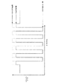
図1に示すように、レーザー構造100の第1の実施例はInP基板10を含む。該基板上には、エピタキシャル成長によりn−InPクラッド層20、活性領域30、p−InPクラッド層40、及びp−InGaAsキャップ層60が形成される。活性領域30は、単一量子井戸構造を含む。単一量子井戸構造は、InAsPの歪み量子井戸へテロ構造活性層32を含む。InAsP量子井戸層32は、脇から障壁層33と34で挟まれる。障壁層はGax(AlIn)1-xP(x≧0)から成る。代替実施形態では、活性領域30がn層のInAsP量子井戸層と(n+1)層のGax(AlIn)1-xP障壁層(x≧0)とから成る多重量子井戸構造を含む場合もある点に注意して欲しい。
As shown in FIG. 1, a first embodiment of the
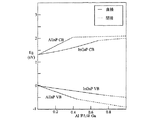
InGaP中のGaの一部又は全てをAlに置換することにより、量子井戸層32の物質と障壁層33、34の物質との間における伝導帯及び価電子帯の不連続性が大きくなる。例えば、図2は、歪みInGaPのバンドエネルギーのGaモル分率に対する依存度と、AlInP(すなわちx=0としたときのGax(AlIn)1-xP)のAlモル分率に対する依存度とを示したグラフである。図2は、AlInP障壁層物質がInGaP障壁層物質よりも高いバンドギャップエネルギーを有することを顕著に示している。障壁層33、34の物質AlInP中の所定のモル分率のAlは、InGaP中の同じモル分率のGaよりも高いバンドギャップエネルギーを作り出すという点に、着目して欲しい。従って、量子井戸層32の物質InAsPと障壁層33、34の物質AlInPとの間のバンドオフセットが大きくなる。バンドオフセットを大きくすることにより、レーザーの閾値電流を著しく増大させることなく高温性能を向上させることが可能になる。
By substituting part or all of Ga in InGaP with Al, the discontinuity of the conduction band and the valence band between the material of the
図3は、Gaモル分率の関数としての無歪みInGaPとAlモル分率の関数としてのAlInPとの間の伝導帯の不連続性を示すグラフである。詳しくは、この不連続性は、障壁層33、34を所与のGaモル分率を有するInGaPに替えて同じAlモル分率を有するAlInPで構成したときの、InAsP量子井戸層32中の電子に対する増加分の障壁を表している。障壁層33、34の物質であるInGaP中のGaをAlで置換することにより、障壁層のバンドエネルギーは図4に示すように増大する。バンドエネルギーを増大させることにより、InAsP量子井戸32中の障壁層によって得られるキャリア閉じ込め能力が向上し、高温性能が改善される。従って、レーザー構造100は従来の長波長光源に比べて優れた温度特性を有する。
FIG. 3 is a graph showing the conduction band discontinuity between unstrained InGaP as a function of Ga mole fraction and AlInP as a function of Al mole fraction. Specifically, this discontinuity is caused by the electron in the InAsP
更に、本発明の障壁層33、34の物質AlInPは、従来の障壁層物質AlInGaAsと異なり、燐(P)とアルミニウム(Al)を含む。これらの成分により、本発明の障壁層物質は、Alと砒素(As)を含む物質よりも、低い成膜温度で良好な結晶品質に作成することが可能になる。この特性は、P(PはAsよりも小さい原子である)が反応性のAlに対して強い結合特性を有することから得られる。そのため、Pを成分に含むAl化合物は、Asを成分に含むAl化合物よりも結晶品質が優れている(成膜温度とAlモル分率を一定に維持した場合)。従って、活性領域30の障壁層33、34の物質として、AlInGaAsに替えてAlInPを用いることにより、量子井戸層の障壁層との界面を良好なものにすることができ、一般的には障壁層物質も良好なものになる。結晶品質の向上により、閾値電流も小さくなる。
Further, the material AlInP of the
これに対応して、特定のレーザー用途では、障壁層物質にAlGaInP(すなわちx=1としたときのGax(AlIn)1-xP)を用いるのが好ましい場合がある。なぜなら、AlGaInPの伝導帯エネルギーは、AlInPの伝導体エネルギーとInGaPの伝導帯エネルギーの間にあるからである。こうすることにより、量子井戸層32の物質に対してバンドオフセットが低くなり、活性領域30中のキャリア分布が良好になる。
Correspondingly, for certain laser applications, it may be preferable to use AlGaInP (ie, Ga x (AlIn) 1-x P when x = 1) as the barrier layer material. This is because the conduction band energy of AlGaInP is between the conduction energy of AlInP and the conduction band energy of InGaP. This reduces the band offset with respect to the material of the
図5A〜図5Dは、本発明のレーザー構造を製造するプロセス500の一実施形態を示す図である。図5Aに示すように、InPの単結晶から成る基板10を用意する。図5Bにおいて、この基板10上に、n−InP(通常、Si、Se又はTeがドープされている)から成る3μmのクラッド層を600℃でエピタキシャル成長させる。次に図5Cにおいて、クラッド層20の上に活性領域30を形成する。この活性領域30は、xを0としたGax(AlIn)1-xPの障壁層33と、InAsPの量子井戸層32と、xを0としたGax(AlIn)1-xPのもう1つの障壁層34とを成膜することにより形成される。InAsP量子井戸層とGax(AlIn)1-xP障壁層は、通常約550℃で成膜され、それぞれ約10nmの厚さに形成される。次に図5Dに示すように、活性領域30の上にp−InPのクラッド層40を成膜する。このp−InPクラッド層40の厚さは通常3μmであり、約600℃で成膜される。p−InPクラッド層40には通常、ドーパントとしてZnが用いられる。最後にp−InGaAs(Znをドープしたもの)のキャップ層60を成膜する。
5A-5D illustrate one embodiment of a process 500 for manufacturing a laser structure of the present invention. As shown in FIG. 5A, a
代替実施形態において、このレーザー構造は、活性領域の反対側に配置された導波路層を含む場合がある。導波路層はInGaAsPまたはAlInGaAsから形成することができる。 In an alternative embodiment, the laser structure may include a waveguide layer located opposite the active region. The waveguide layer can be formed from InGaAsP or AlInGaAs.
あるいは、活性領域30は、更なる量子井戸層とそれに対応する数の障壁層とから成る複数の量子井戸構造を含んでもよい。通常、InAsP量子井戸層は、InP基板上に成膜された場合、圧縮歪みを有する。InAsPの量子井戸層を有するレーザーでは、この圧縮歪みにより、透明度が低下し、微分利得が大きくなる。このことは、効率が高く高速なデバイスが得られるという重要な可能性を示唆するものである。しかしながら、InAsP量子井戸層における圧縮歪みの大きさ(典型的には、InAsP中のAsが40%のとき約1.25%の歪みが生じる)は、量子井戸層の物質InAsPが歪み限界に到達するまでに追加し得るInAsP量子井戸層の数に制限を与える。従って、この圧縮歪みを相殺するため、障壁層33、34に使用されるGax(AlIn)1-xPに引張歪みが加えられる場合がある。この引張歪みの大きさは、Gax(AlIn)1-xP中のInとGaの相対的な組成を変えることにより容易に変化させることができる。障壁層32、34のGax(AlIn)1-xPにおいてx=0.15としたとき、通常1%の引張歪みが得られる。
Alternatively,
本発明の上記の実施形態は、考え得る実施形態の例を説明しただけであり、本発明を分かりやすく理解する目的で提示したものに過ぎない。本発明の上記の実施形態には、本発明の原理から実質的に外れることなく、多数の変更や修正を加えることが可能である。例えば、レーザー構造のInAsP/Gax(AlIn)1-xP活性領域30の外にある層は、数や構成が例示したものと異なっていてもよいと考えられる。エッチングや層順序の入れ替え等、追加の製造工程を実施することも可能である。その結果、本発明に従い、多種のデバイスを形成することが出来る。そのような変更形態や修正形態もすべて本発明の開示範囲に含まれ、特許請求の範囲によって保護されるものとする。
The above-described embodiments of the invention have been described only by way of example of possible embodiments and are merely presented for the purpose of making the invention easier to understand. Numerous changes and modifications can be made to the above-described embodiments of the present invention without departing substantially from the principles of the present invention. For example, it is believed that the layers outside the InAsP / Ga x (AlIn) 1-x P
10 基板
20 第1のクラッド層
32 量子井戸層
33 第1の障壁層
34 第2の障壁層
40 第2のクラッド層
60 キャップ層
100 レーザー構造
DESCRIPTION OF
Claims (10)
基板(10)を設けるステップと、
前記基板(10)上に第1のクラッド層(20)を形成するステップと、
前記第1のクラッド層(20)の上に、Gax(AlIn)1-xP(x≧0)を含む第1の障壁層(33)を形成するステップと、
前記第1の障壁層(33)の上に、前記第1の障壁層(33)よりも低いバンドギャップエネルギーを有するInAsP量子井戸層(32)を形成するステップと、
前記量子井戸層(32)の上に、前記量子井戸層(32)よりも高いバンドギャップエネルギーを有し、Gax(AlIn)1-xP(x≧0)を含む第2の障壁層(34)を形成するステップと、
前記第2の障壁層(34)の上に第2のクラッド層(40)を形成するステップと、
からなる方法。 A method (500) for producing a laser structure (100) operable at elevated temperatures,
Providing a substrate (10);
Forming a first cladding layer (20) on the substrate (10);
Forming a first barrier layer (33) containing Ga x (AlIn) 1-x P (x ≧ 0) on the first cladding layer (20);
Forming an InAsP quantum well layer (32) having a lower bandgap energy than the first barrier layer (33) on the first barrier layer (33);
On the quantum well layer (32), a second barrier layer having a higher band gap energy than the quantum well layer (32) and containing Ga x (AlIn) 1-x P (x ≧ 0) 34) forming
Forming a second cladding layer (40) on the second barrier layer (34);
Method consisting of.
前記第2の量子井戸層の上且つ前記第2のクラッド層(40)の下に、前記第2の量子井戸層よりも高いバンドギャップエネルギーを有するGax(AlIn)1-xP(x≧0)の第3の障壁層を形成するステップと、
を更に含む、請求項7の方法(500)。
Forming a second quantum well layer made of InAsP having a lower bandgap energy than the second barrier layer (34) on the second barrier layer (34);
Above the second quantum well layer and below the second cladding layer (40), Ga x (AlIn) 1-x P (x ≧ 2) having a higher band gap energy than the second quantum well layer. 0) forming a third barrier layer;
The method (500) of claim 7, further comprising:
Applications Claiming Priority (1)
| Application Number | Priority Date | Filing Date | Title |
|---|---|---|---|
| US10/354,276 US6730944B1 (en) | 2003-01-30 | 2003-01-30 | InP based high temperature lasers with InAsP quantum well layers and barrier layers of Gax(ALIn)1-xP |
Publications (2)
| Publication Number | Publication Date |
|---|---|
| JP2004235628A true JP2004235628A (en) | 2004-08-19 |
| JP2004235628A5 JP2004235628A5 (en) | 2007-03-01 |
Family
ID=32176329
Family Applications (1)
| Application Number | Title | Priority Date | Filing Date |
|---|---|---|---|
| JP2004007511A Withdrawn JP2004235628A (en) | 2003-01-30 | 2004-01-15 | InP-BASED HIGH-TEMPERATURE LASER HAVING InAsP QUANTUM WELL LAYER AND Gax(AlIn) l-xP BARRIER LAYER |
Country Status (4)
| Country | Link |
|---|---|
| US (1) | US6730944B1 (en) |
| EP (1) | EP1443616B1 (en) |
| JP (1) | JP2004235628A (en) |
| DE (1) | DE60311412T2 (en) |
Families Citing this family (7)
| Publication number | Priority date | Publication date | Assignee | Title |
|---|---|---|---|---|
| KR101866495B1 (en) * | 2014-11-11 | 2018-06-11 | 피니사 코포레이숀 | Two-stage Adiabatically Coupled Photonic Systems |
| EP4160833A1 (en) | 2015-12-17 | 2023-04-05 | Finisar Corporation | Surface coupled systems |
| US10992104B2 (en) | 2015-12-17 | 2021-04-27 | Ii-Vi Delaware, Inc. | Dual layer grating coupler |
| WO2018106834A1 (en) | 2016-12-06 | 2018-06-14 | Finisar Corporation | Surface coupled laser with optical interposer |
| US10809456B2 (en) | 2018-04-04 | 2020-10-20 | Ii-Vi Delaware Inc. | Adiabatically coupled photonic systems with fan-out interposer |
| US11435522B2 (en) | 2018-09-12 | 2022-09-06 | Ii-Vi Delaware, Inc. | Grating coupled laser for Si photonics |
| US11404850B2 (en) | 2019-04-22 | 2022-08-02 | Ii-Vi Delaware, Inc. | Dual grating-coupled lasers |
Family Cites Families (2)
| Publication number | Priority date | Publication date | Assignee | Title |
|---|---|---|---|---|
| JP2914210B2 (en) * | 1995-03-07 | 1999-06-28 | 日本電気株式会社 | Multiple quantum well structure optical semiconductor device and method of manufacturing the same |
| JP2003243693A (en) * | 2002-02-19 | 2003-08-29 | Oki Electric Ind Co Ltd | Semiconductor light receiving element and semiconductor component |
-
2003
- 2003-01-30 US US10/354,276 patent/US6730944B1/en not_active Expired - Fee Related
- 2003-09-18 DE DE60311412T patent/DE60311412T2/en not_active Expired - Lifetime
- 2003-09-18 EP EP03021206A patent/EP1443616B1/en not_active Expired - Fee Related
-
2004
- 2004-01-15 JP JP2004007511A patent/JP2004235628A/en not_active Withdrawn
Also Published As
| Publication number | Publication date |
|---|---|
| EP1443616A3 (en) | 2005-11-30 |
| EP1443616B1 (en) | 2007-01-24 |
| DE60311412T2 (en) | 2007-10-31 |
| DE60311412D1 (en) | 2007-03-15 |
| EP1443616A2 (en) | 2004-08-04 |
| US6730944B1 (en) | 2004-05-04 |
Similar Documents
| Publication | Publication Date | Title |
|---|---|---|
| US20050040384A1 (en) | Semiconductor light-emitting element and method of manufacturing the same | |
| JP4554526B2 (en) | Semiconductor light emitting device | |
| US10020637B2 (en) | Method for manufacturing semiconductor device and semiconductor device | |
| JP2004235628A (en) | InP-BASED HIGH-TEMPERATURE LASER HAVING InAsP QUANTUM WELL LAYER AND Gax(AlIn) l-xP BARRIER LAYER | |
| JP2009141188A (en) | Integrated semiconductor optical device | |
| JP2004253802A (en) | GaAsSb/GaAs DEVICE WITH IMPROVED TEMPERATURE PROPERTY | |
| JP2000058964A (en) | Quantum-well structured optical semiconductor element | |
| US20170324219A1 (en) | Semiconductor laser incorporating an electron barrier with low aluminum content | |
| JPH08274295A (en) | Manufacture of optical semiconductor device | |
| JP2005039045A (en) | Quantum cascade laser | |
| US20180269658A1 (en) | Semiconductor laser incorporating an electron barrier with low aluminum content | |
| JP2011023493A (en) | Semiconductor laser | |
| US20080013579A1 (en) | Buried-heterostructure semiconductor laser | |
| JP6487236B2 (en) | Semiconductor optical device and manufacturing method thereof | |
| JP7038913B1 (en) | Semiconductor laser device | |
| JPH1197790A (en) | Semiconductor laser | |
| JP6158591B2 (en) | Semiconductor laser | |
| JP2001332816A (en) | Semiconductor laser element | |
| JP7296845B2 (en) | MODULATION DOPED SEMICONDUCTOR LASER AND MANUFACTURING METHOD THEREOF | |
| JP2005260109A (en) | Optical semiconductor element | |
| JP5373585B2 (en) | Semiconductor laser and electroabsorption modulator integrated distributed feedback laser | |
| JP2000353861A (en) | Manufacture of iii-v semiconductor light emitting device | |
| JP4178901B2 (en) | Semiconductor optical device and method of manufacturing semiconductor optical device | |
| CN112398003A (en) | Modulation doped semiconductor laser and method for manufacturing the same | |
| JP2010109237A (en) | Optical phase control element and semiconductor light-emitting element |
Legal Events
| Date | Code | Title | Description |
|---|---|---|---|
| A521 | Request for written amendment filed |
Free format text: JAPANESE INTERMEDIATE CODE: A523 Effective date: 20070115 |
|
| A621 | Written request for application examination |
Free format text: JAPANESE INTERMEDIATE CODE: A621 Effective date: 20070115 |
|
| A711 | Notification of change in applicant |
Free format text: JAPANESE INTERMEDIATE CODE: A711 Effective date: 20070319 |
|
| A761 | Written withdrawal of application |
Free format text: JAPANESE INTERMEDIATE CODE: A761 Effective date: 20070427 |