JP2004233824A - Multibeam scanner - Google Patents
Multibeam scanner Download PDFInfo
- Publication number
- JP2004233824A JP2004233824A JP2003024138A JP2003024138A JP2004233824A JP 2004233824 A JP2004233824 A JP 2004233824A JP 2003024138 A JP2003024138 A JP 2003024138A JP 2003024138 A JP2003024138 A JP 2003024138A JP 2004233824 A JP2004233824 A JP 2004233824A
- Authority
- JP
- Japan
- Prior art keywords
- light
- scanning
- emitting point
- light emitting
- emitted
- Prior art date
- Legal status (The legal status is an assumption and is not a legal conclusion. Google has not performed a legal analysis and makes no representation as to the accuracy of the status listed.)
- Granted
Links
Images


Classifications
-
- G—PHYSICS
- G02—OPTICS
- G02B—OPTICAL ELEMENTS, SYSTEMS OR APPARATUS
- G02B26/00—Optical devices or arrangements for the control of light using movable or deformable optical elements
- G02B26/08—Optical devices or arrangements for the control of light using movable or deformable optical elements for controlling the direction of light
- G02B26/10—Scanning systems
- G02B26/12—Scanning systems using multifaceted mirrors
- G02B26/123—Multibeam scanners, e.g. using multiple light sources or beam splitters
-
- B—PERFORMING OPERATIONS; TRANSPORTING
- B41—PRINTING; LINING MACHINES; TYPEWRITERS; STAMPS
- B41J—TYPEWRITERS; SELECTIVE PRINTING MECHANISMS, i.e. MECHANISMS PRINTING OTHERWISE THAN FROM A FORME; CORRECTION OF TYPOGRAPHICAL ERRORS
- B41J2/00—Typewriters or selective printing mechanisms characterised by the printing or marking process for which they are designed
- B41J2/435—Typewriters or selective printing mechanisms characterised by the printing or marking process for which they are designed characterised by selective application of radiation to a printing material or impression-transfer material
- B41J2/47—Typewriters or selective printing mechanisms characterised by the printing or marking process for which they are designed characterised by selective application of radiation to a printing material or impression-transfer material using the combination of scanning and modulation of light
- B41J2/471—Typewriters or selective printing mechanisms characterised by the printing or marking process for which they are designed characterised by selective application of radiation to a printing material or impression-transfer material using the combination of scanning and modulation of light using dot sequential main scanning by means of a light deflector, e.g. a rotating polygonal mirror
- B41J2/473—Typewriters or selective printing mechanisms characterised by the printing or marking process for which they are designed characterised by selective application of radiation to a printing material or impression-transfer material using the combination of scanning and modulation of light using dot sequential main scanning by means of a light deflector, e.g. a rotating polygonal mirror using multiple light beams, wavelengths or colours
-
- H—ELECTRICITY
- H04—ELECTRIC COMMUNICATION TECHNIQUE
- H04N—PICTORIAL COMMUNICATION, e.g. TELEVISION
- H04N1/00—Scanning, transmission or reproduction of documents or the like, e.g. facsimile transmission; Details thereof
- H04N1/04—Scanning arrangements, i.e. arrangements for the displacement of active reading or reproducing elements relative to the original or reproducing medium, or vice versa
- H04N1/113—Scanning arrangements, i.e. arrangements for the displacement of active reading or reproducing elements relative to the original or reproducing medium, or vice versa using oscillating or rotating mirrors
- H04N1/1135—Scanning arrangements, i.e. arrangements for the displacement of active reading or reproducing elements relative to the original or reproducing medium, or vice versa using oscillating or rotating mirrors for the main-scan only
-
- H—ELECTRICITY
- H04—ELECTRIC COMMUNICATION TECHNIQUE
- H04N—PICTORIAL COMMUNICATION, e.g. TELEVISION
- H04N1/00—Scanning, transmission or reproduction of documents or the like, e.g. facsimile transmission; Details thereof
- H04N1/04—Scanning arrangements, i.e. arrangements for the displacement of active reading or reproducing elements relative to the original or reproducing medium, or vice versa
- H04N1/19—Scanning arrangements, i.e. arrangements for the displacement of active reading or reproducing elements relative to the original or reproducing medium, or vice versa using multi-element arrays
- H04N1/191—Scanning arrangements, i.e. arrangements for the displacement of active reading or reproducing elements relative to the original or reproducing medium, or vice versa using multi-element arrays the array comprising a one-dimensional array, or a combination of one-dimensional arrays, or a substantially one-dimensional array, e.g. an array of staggered elements
- H04N1/1911—Simultaneously or substantially simultaneously scanning picture elements on more than one main scanning line, e.g. scanning in swaths
Abstract
Description
【0001】
【発明の属する技術分野】
本発明はマルチビーム走査装置に関し、特に光源手段から射出した光束を偏向手段としてのポリゴンミラーにより反射偏向させ、走査光学系を介して被走査面上を光走査して画像情報を記録するようにした、例えば電子写真プロセスを有するレーザービームプリンターやデジタル複写機やマルチファンクションプリンター(多機能プリンタ)等の画像形成装置に好適なものである。
【0002】
特に複数の光束を同時に光走査して高速化・高精細化を図ったマルチビーム走査装置において、ポリゴンミラー等の偏向手段を効率良く使用することにより装置全体の小型化を図ったものである。
【0003】
【従来の技術】
図21は従来のマルチビーム走査装置の要部概略図である。
【0004】
同図において画像情報に応じて光源手段91から光変調され出射した2つの光束はコリメーターレンズ92により略平行光束に変換され、シリンドリカルレンズ93に入射する。シリンドリカルレンズ93に入射した光束のうち主走査断面内においてはそのままの状態で出射して開口絞り94を通過する(一部遮光される)。また副走査断面内においては収束して開口絞り94を通過し(一部遮光される)光偏向器95の偏向面95aにほぼ線像(主走査方向に長手の線像)として結像する。そして光偏向器95の偏向面95aで反射偏向された2つの光束は各々走査光学系(走査レンズ)96により感光ドラム面97上にスポット状に結像され、該光偏向器95を矢印A方向に回転させることによって、該感光ドラム面97上を矢印B方向(主走査方向)に等速度で光走査している。これにより記録媒体である感光ドラム面97上に2本の走査線を同時に形成し、画像記録を行っている。
【0005】
このとき感光ドラム面97上を光走査する前に該感光ドラム面97上の走査開始位置のタイミングを調整する為に、光偏向器95で反射偏向された2つの光束の一部(BD光束)を走査光学系96により同期検出手段用の折り返しミラー(BDミラー)98を介して同期検出手段用の光検出素子(BDセンサー)99に導光している。そしてBDセンサー99からの出力信号を検知して得られた同期信号(BD信号)を用いて感光ドラム面97上への画像記録の走査開始位置のタイミングを各BD光束毎に調整している。尚、同図に描いた光束は分かりやすくする為に全て主光束のみを描いている。
【0006】
この種のマルチビーム走査装置において高品位な画像を得る為に走査線を書き始める前に各光束の発光量を調整(以下「オートパワーコントロール(APC)」とも称す。)し、感光ドラム面上へ照射される光量が常に一定となるようにしている。
【0007】
また同期検知(BD検知)と光源手段から発せられた複数の光束の光量調整(APC)を行うための光量モニターを有し、該複数の光束を順次に同期検知および光量調整を行うマルチビーム走査装置が提案されている。
【0008】
【発明が解決しようとする課題】
しかしながらこれら従来のマルチビーム走査装置は光源手段の発光順序まで言及したものはなく、光偏向器(ポリゴンミラー)を有効に使用できないことから大型な光偏向器を用いる必要があった。
【0009】
また光偏向器の偏向面の端部に面取りがなされている場合においては、面取り部に入射した光束が感光ドラム面上へ到達することとなり、ゴーストの問題が発生する虞があった。
【0010】
本発明は偏向手段の小型化を図ることができるマルチビーム走査装置の提供を目的とする。また本発明はゴースト光が発生しない常に良好なる画像が得られるマルチビーム走査装置の提供を目的とする。
【0011】
【課題を解決するための手段】
本発明のマルチビーム走査装置は、
主走査方向に離間して配置された複数の発光点を有する光源手段と、該光源手段から発せられた複数の光束を被走査面へ向けて偏向する偏向手段とを有するマルチビーム走査装置において、
該光源手段から発せられた複数の光束のうち、主走査方向において該偏向手段の偏向面の中心から最も離れた位置に到達する光束を発光するのを第1の発光点とし、別の光束を発光するのを第2の発光点としたとき、該偏向手段にて偏向可能な角度範囲内にあって、該光束を該被走査面上の有効走査範囲へ向けて偏向する際の有効走査角度範囲よりも、該偏向手段の回転方向上流側に存在する上流側外部角度範囲において、該第2の発光点を最初に発光させたことを特徴としている。
【0012】
【発明の実施の形態】
(実施形態1)
図1は本発明の実施形態1のマルチビーム走査装置の主走査方向の要部断面図(主走査断面図)である。
【0013】
ここで、主走査方向とは偏向手段の回転軸及び走査光学素子の光軸に垂直な方向(偏向手段で光束が反射偏向(偏向走査)される方向)を示し、副走査方向とは偏向手段の回転軸と平行な方向を示す。また主走査断面とは主走査方向に平行で走査光学系の光軸を含む平面を示す。また副走査断面とは主走査断面と垂直な断面を示す。
【0014】
同図において1は光源手段であり、2つの発光点1a,1bを有するモノリシックな半導体レーザアレイより成っている。2つの発光点1a,1bは主走査方向及び副走査方向に対して各々離れて配置されている。
【0015】
2は集光レンズ系(コリメーターレンズ)であり、1枚のレンズより成り、光源手段1より出射された2つの光束BMa,BMbを略平行光束(もしくは略発散光束もしくは略収束光束)に変換している。3はレンズ系(シリンドリカルレンズ)であり、副走査方向のみに所定の屈折力を有している。4は開口絞りであり、シリンドリカルレンズ3より出射された2つの光束BMa,BMbを所望の最適なビーム形状に成形している。
【0016】
尚、コリメーターレンズ2、シリンドリカルレンズ3、開口絞り4等の各要素は入射光学手段の一要素を構成している。
【0017】
5は偏向手段としての光偏向器であり、例えば6面構成の回転多面鏡(ポリゴンミラー)より成り、モータ−等の駆動手段(不図示)により図中矢印A方向に一定速度で回転している。
【0018】
7は結像性能とfθ特性を有する走査光学系であり、1枚の走査レンズより成り、光偏向器5により偏向された2つの光束BMa,BMbを被走査面としての感光ドラム面8上にスポット状に結像させ、2本の走査線を形成している。走査レンズ7は副走査断面内において光偏向器5の偏向面5a近傍と感光ドラム面8近傍との間を共役関係にすることにより、倒れ補正機能を有している。
【0019】
8は被走査面としての感光ドラム面、8aは有効走査範囲である。
【0020】
9は同期検出用の折り返しミラー(以下、「BDミラー」と記す。)であり、感光ドラム面8上の走査開始位置のタイミングを調整するための2つの同期検出用の光束(BD光束)を同期検出手段10側へ反射させている。
【0021】
10は同期検出手段であり、同期検出用のスリット(以下、「BDスリット」と記す。)10aと同期検出素子としての光センサー(以下、「BDセンサー」と記す。)10bとを有しており、BDセンサー10bからの出力信号を検知して得られた同期信号(BD信号)を用いて感光ドラム面8上への画像記録の走査開始位置のタイミングを調整している。BDスリット10aは感光ドラム面8と光学的に等価な位置に配されており、画像の書き出し位置を決めている。
【0022】
尚、BDミラー9、BDスリット10a、そしてBDセンサー10b等の各要素は同期検出光学系(BD光学系)の一要素を構成している。
【0023】
本実施形態において画像情報に応じて光源手段1から光変調され出射した2本の光束BMa,BMbはコリメーターレンズ2により略平行光束に変換され、シリンドリカルレンズ3に入射する。シリンドリカルレンズ3に入射したレーザ光束のうち主走査断面内においてはそのままの状態で出射して開口絞り4を通過する(一部遮光される)。また副走査断面内においては収束して開口絞り4を通過し(一部遮光される)光偏向器5の偏向面5aにほぼ線像(主走査方向に長手の線像)として結像する。そして光偏向器5の偏向面5aで反射偏向された2本の光束BMa,BMbは各々走査レンズ7により感光ドラム面8上にスポット状に結像され、該光偏向器5を矢印A方向に回転させることによって、該感光ドラム面8上を矢印B方向(主走査方向)に等速度で光走査している。これにより記録媒体である感光ドラム面8上に2本の走査線を同時に形成し、画像記録を行っている。
【0024】
このとき感光ドラム面8上を光走査する前に該感光ドラム面8上の走査開始位置のタイミングを調整する為に、光偏向器5で反射偏向された2つの光束BMa,BMbの一部(BD光束)をBDミラー9を介してBDスリット10a面上に集光させた後、BDセンサー10bに導光している。そしてBDセンサー10bからの出力信号を検知して得られた同期信号(BD信号)を用いて感光ドラム面8上への画像記録の主走査方向の走査開始位置のタイミングを各BD光束毎に調整している。
【0025】
図2は本発明の実施形態1のマルチビーム走査装置の要部概要図である。同図において図1に示した要素と同一要素には同符番を付している。
【0026】
同図において光偏向器5の偏向面5aにて、光源手段1から発せられた光束を偏向できる範囲はある角度範囲に限られる。図中の「偏向可能な角度範囲」8cがそれであり、走査効率100%の角度範囲であって、光偏向器5の面数をC(面)としたとき、偏向可能な角度θc(rad)は次式で表される範囲となる。
【0027】
【数1】

本実施形態では光偏向器5の面数C=6(面)であり、偏向可能な角度θc(rad)は、▲1▼式より
【0029】
【数2】
の範囲である。
【0031】
走査光学系の場合、偏向角(画角)と走査位置とは1対1に対応するので、範囲を指定する際には偏向角を用いても良いし、走査位置を用いても良い。
【0032】
前述した「偏向可能な角度範囲」8cの中央部には通常「有効走査角度範囲」8bがあり、その走査位置に対応するのが「有効走査範囲」8aであって、感光ドラム面8上に潜像を形成する範囲である。また「有効走査角度範囲」8bより光偏向器5の回転方向の上流側にも「偏向可能な角度範囲」8cの一部である「上流側外部角度範囲」8dがあり、同期検出手段10へ向う光束(BD光束)BMbdはこの角度範囲に存在する。下流側には「下流側外部角度範囲」8eがあり、ここにも同期検出手段10へ向う光束(BD光束)を存在させる場合もある。
【0033】
従来のシングルビーム走査装置のときから、同期検出手段10へ向けて偏向させる場合等、光偏向器5によって光束が偏向される角度が「有効走査角度範囲」よりも外側の「上流側外部角度範囲」や「下流側外部角度範囲」にある場合は、偏向面5aの端部近傍を用いて光源手段1から発せられた光束を反射偏向させており、光束の端から偏向面5aの端部までにはあまり余裕がなかった。
【0034】
本実施形態では後述するように光源手段1から発せられた2本の光束BMa,BMbのうち、主走査方向において光偏向器5の偏向面の中心から最も離れた位置に到達する光束を発光するのを第1の発光点とし、別の光束を発光するのを第2の発光点としたとき、該光偏向器5にて偏向可能な角度範囲内8cにあって、該光束を感光ドラム面8上の有効走査範囲8aへ向けて偏向する際の有効走査角度範囲8bよりも、該光偏向器5の回転方向上流側に存在する上流側外部角度範囲8dにおいて、該第2の発光点を最初に発光させている。
【0035】
図3は同期検出手段10における光検知の様子を説明する図である。同期検出手段10では、図中実線aで示したグラフの様にBDスリット10aを通過してBDセンサー10bで検出される光量が時間と共に増加しており、閾値に達した瞬間(時間)を検出している。そして検出した瞬間から一定時間後に発光を開始し、被走査面8上の主走査方向の走査開始位置を揃えている。
【0036】
図4は光源手段1の2つの発光点1a,1bの配置を示した図である。本実施形態におけるマルチビーム走査装置では、被走査面8上の走査線間隔が画素密度に応じた所定の間隔となるように光源手段1を光軸を中心に角度δ回転させて調整している。このとき2つの発光点1a,1bは副走査方向に間隔Dsだけ離間すると共に主走査方向にも間隔Dmだけ離間して配置されている。
【0037】
図5は本実施形態におけるマルチビーム走査装置の主走査方向における要部概要図である。同図において図1に示した要素と同一要素には同符番を付している。同図は光源手段1から発せられた光束を光偏向器5によって同期検出手段10へ向けて反射偏向する様子を模式的に示している。
【0038】
本実施形態のマルチビーム走査装置において2つの発光点1a,1bは主走査方向に離間して配置されており、夫々の発光点1a,1bから発せられた2本の光束BMa,BMbは偏向面5a上で主走査方向に離れた位置に到達する。そのため光源手段1から発せられた2本の光束BMa,BMbを光偏向器5の偏向面5aにより例えば同期検出手段10へ向けて偏向させる場合、2本の光束には偏向面5aの中心に近い位置に到達する光束BMa(実線)と偏向面5aの中心から遠い位置に到達する光束BMb(破線)とが存在する。偏向面5aの中心から遠い位置に到達する光束BMbは偏向面5aに全光束が収まらず、偏向面5aで蹴られてしまう虞がある。
【0039】
偏向面5aにて蹴られた光束BMbが同期検出手段10に入射するとBDセンサー10bによって検出される光量が減少する。すると図3中の破線bで示したグラフの様に閾値を越える光量に達するまでに時間が掛かり、タイミングが遅れて走査開始位置がずれる問題が発生する。特にマルチビーム走査装置の場合、光束毎に偏向面5aで蹴られる光量が異なるので各光束に対応した走査線毎に走査開始位置がばらつき画質が劣化して問題となる。よって光源手段1からの光束が偏向面5aにて蹴られるのは大きな問題である。
【0040】
しかしながら偏向面5aを大きくすると光偏向器5が大型化するのみならず、該光偏向器5を回転駆動させる駆動手段もトルクが必要となってコスト的なデメリットも大きい。
【0041】
そこで本実施形態では偏向面5aを効率良く使用することにより、上記の問題点を解決している。
【0042】
即ち、光源手段1から発せられた2本の光束のうち、主走査方向において光偏向器5の偏向面5aに最初に入射する光束を発光する発光点を他の発光点よりも先に発光させている。
【0043】
具体的には同期検出手段10へ導光する際に偏向面5aに到達する2本の光束BMa,BMbのうち、偏向面5aの中心から最も近い位置に到達する光束BMaを発光する発光点(第2の発光点)1aを先に発光させて同期検知(BD検知)を行い、その後、光偏向器5が矢印Aの方向に回転することにより偏向面5aが移動して蹴られなくなるのを待って偏向面5aの中心から離れた位置に到達する光束BMbを発光する発光点(第1の発光点)1bを発光させて同期検知を行っている。
【0044】
ここで、2本の光束BMa,BMbは同期検知を取る位置が異なるが、同期検出手段10のスリット10aの位置を2箇所に設けることで簡単に対処できる。また夫々の光束BMa,BMbに対して同期検出手段10を設けても良い。
【0045】
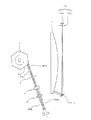
図6A〜図6Eは各々偏向面5a上に到達する2本の光束BMa,BMbの様子を模式的に示した図である。図6A〜図6Eにおいて図1に示した要素と同一要素には同符番を付している。本実施形態において光源手段1から発せられた2本の光束BMa,BMbは偏向面5a上で異なる位置に到達する。
【0046】
図6Aは同期検出手段(不図示)へ向けて発光点(第2の発光点)1aからの光束BMaを偏向する様子を示した図であり、光束BMaは偏向面5aにより全光束が反射偏向されているのに対して発光点(第1の発光点)1bからの光束BMbは偏向面5aの端部を跨ぎ光束の一部が蹴られている。
【0047】
図6Bは同期検出手段(不図示)へ向けて光束BMbを偏向する様子を示した図であり、光束BMbも偏向面5aにより全光束が反射偏向されている。
【0048】
図6Cは被走査面上の走査有効範囲内へ各光束を偏向する様子を示した図であり、各光束BMa,BMb共に偏向面5aの中央付近に到達している。
【0049】
図6Dは被走査面上の走査有効範囲を越えた位置へ向けて各光束を偏向する様子を示した図である。今度は光束BMaが偏向面5aの中心から離れた位置に到達し、光束BMbが偏向面5aの中心に近い位置に到達している。
【0050】
図6Eは図6Dの直後の様子を示した図であり、光束BMaは偏向面5aの端部を跨ぎ、光束の一部が蹴られているのに対して光束BMbは偏向面5aにより全光束が反射偏向される。
【0051】
図6A〜図6Eを時系列に並べると、図6A→図6B→図6C→図6D→図6Eであり、偏向面5a上を2本の光束BMa,BMbが移動していることが分かる。2本の光束BMa,BMbは実際には移動しないが、光偏向器5が回転するので偏向面5aから相対的にみると移動しているのである。
【0052】
図6Aでは光束BMaのみが全光束を反射偏向されることができるが、少し時間が経過して図6Bの状態となれば光束BMbも全光束を反射偏向されることができるのである。
【0053】
本実施形態では偏向面5aにより全ての光束が反射偏向されることができるようになったところで同期検知を行っており、該同期検知の為に発光する順番を光束BMaを発光する発光点(第2の発光点)1aが先で光束BMbを発光する発光点(第1の発光点)1bを後としている。
【0054】
また本実施形態において2本の光束BMa,BMbは開口絞り4にて交差しており、光源手段1から偏向面5aの間で交差するのはこの1回のみである。故に交差した回数MはM=2×n+1=1(n=0)である。この場合、走査開始前に偏向面5aの中心の近くに到達するのは、光偏向器5の回転方向Aの下流側に配置された光束BMaを発光する発光点1aであり、偏向面5aの中心から離れた位置に到達するのは光偏向器5の回転方向Aの上流側に配置された光束BMbを発光する発光点1bである。
【0055】
そこで本実施形態では上記の如く光偏向器5の回転方向の最も上流側に位置する発光点を第1の発光点とし、下流側に位置する発光点を第2の発光点としたとき、光束BMaを発光する第2の発光点1aを先に発光させて同期検知を行い、次に光束BMbを発光する第1の発光点1bを発光させて同期検知を行っている。これにより光偏向器5を大型化しなくとも安定した同期検知が行えるので省スペースが図られ、マルチビーム走査装置をコンパクト化できる。またシングルビームと同様の光偏向器が流用でき、且つ駆動手段のコストアップを防げるのでコスト的にもメリットが大きい。
【0056】
言い換えれば本実施形態の効果を用いることにより、コンパクト化された常に良好なる画像が得られる簡易な構成のマルチビーム走査装置を提供することができる。
【0057】
このように本実施形態においては上記の如く光偏向器5の回転方向の最も下流側に位置する発光点(第2の発光点)1aを先に発光させて同期検知を行い、次に発光点(第1の発光点)1bを発光させて同期検知を行うことにより、偏向面を有効的に使用可能となり、光偏向器を小型にすることができる。更に光偏向器の駆動手段に必要となるトルクを減少することができる。また光偏向器の面取り部などで発生するゴースト光を回避することができ、常に良好なる画像が得られる。
【0058】
尚、本実施形態では上流側外部角度範囲8dにてBD光束を存在させたが、下流側外部角度範囲8eにおいて該BD光束を存在させても良い。
【0059】
(実施形態2)
図7は本発明の実施形態2のマルチビーム走査装置の主走査断面図である。同図において図1に示した要素と同一要素には同符番を付している。
【0060】
本実施形態において前述の実施形態1と異なる点は、光源手段1の発光点を4つにした点である。その他の構成及び光学的作用は実施形態1と略同様であり、これにより同様な効果を得ている。
【0061】
即ち、同図において1は光源手段であり、例えば4つの発光点1a,1b,1c,1dを有するモノリシックな半導体レーザーアレイより成っている。4つの発光点1a,1b,1c,1dは主走査方向及び副走査方向に対して各々離れて配置されている。
【0062】
図8は偏向面5a上に到達する光源手段1からの4本の光束BMa,BMb,BMc,BMdの様子を模式的に示した図である。図9は図8の4本の光束BMa,BMb,BMc,BMdの主光線(光束の中心線)のみを示した図である。図8,図9において図7に示した要素と同一要素には同符番を付している。
【0063】
本実施形態において光源手段1から発せられた4本の光束BMa(実線),BMb(小破線),BMc(2点鎖線),BMd(大破線)は、開口絞り4にて交差して光偏向器5の偏向面5aへ入射している。本実施形態においても光源手段1から光偏向器5の偏向面5aまで各光束が交差するのは1回である。
【0064】
尚、本実施形態における光偏向器5の内接円の直径は40mmである。
【0065】
本実施形態では前述の実施形態1と同様に光偏向器5の偏向面5a上で4本の光束BMa,BMb,BMc,BMdは夫々異なる位置に到達している。故に主走査断面内において偏向面5a上の広範囲に渡って4本の光束BMa,BMb,BMc,BMdが到達している。
【0066】
ここで偏向面5a上に到達する4本の光束BMa,BMb,BMc,BMdの広がりTm(mm)を求める。
【0067】
主走査方向の光束幅Wm(mm)と隣り合う光束のばらつきΔTm(mm)とビーム数n(本)、及び光束の偏向面5aへの入射角γ(rad)から4本の光束の広がりTm(mm)は次式のように表される。
【0068】
【数3】
夫々の発光点1a,1b,1c,1dから発せられた4本の光束BMa,BMb,BMc,BMdは互いに平行とはならず、ある角度αを有している。集光レンズ系2を通過した後の主走査方向において、互いの光束がなす角度α(rad)は隣り合う発光点の主走査方向の間隔Dm(mm)と集光レンズ系2の焦点距離fcol(mm)によって次式の関係が成立する。
【0070】
【数4】
集光レンズ系2を出射し、シリンドリカルレンズ3を通過して開口絞り4へ到達する際に角度αを有しており、該開口絞り4にて互いの光束が交差して光偏向器5へ角度αを有したまま入射する。
【0072】
このとき隣り合う光束のばらつきΔTm(mm)に対しては、各光束が交差する位置のうち最も偏向面5aに近い位置から偏向面5aまでの距離Lap(mm)が重要となる。本実施形態の場合、各光束が交差する位置のうち最も偏向面5aに近い位置は開口絞り4の位置である。開口絞り4は物理的な要因で偏向面5aの近くに配置することができない。
【0073】
ここで開口絞り4と偏向面5aの間隔Lap(mm)と互いの光束が成す角度α(rad)とから隣り合う光束のばらつきΔTm(mm)は次式で表される。
【0074】
【数5】
![]()
▲3▼、▲5▼式より4本の光束の広がりTm(mm)は次式で表される。
【0076】
【数6】
もしくは、▲4▼、▲5▼式より隣り合う光束のばらつきΔTm(mm)は
【0078】
【数7】
で表され、▲3▼、▲7▼式より4本の光束の広がりTm(mm)は次式で表される。
【0080】
【数8】
つまり主走査方向に離間して配置された4つの発光点を有するマルチビーム走査装置では、隣り合う光束がばらつく分だけ偏向面5a上での4本の光束の広がりTm(mm)が大きくなり、シングルビーム走査装置よりも大きな偏向面5aが必要となる。これは光偏向器5が大型化してマルチビーム走査装置も大型化すると共に大きく重たい光偏向器(ポリゴンミラー)を速く回転させる為にポリゴンモーターのトルクを大きくする必要があり、コストアップを招く問題点があった。またビーム数n(本)が増えるにしたがって偏向面5aを大きくする必要があった。
【0082】
そこで本実施形態では光偏向器5の回転方向Aの最も上流側に配置された発光点(第1の発光点)1dから発せられた光束BMdが偏向面5aの中心から最も離れた位置に到達するので、それ以外の光束を最初に発光させている。偏向面5aの中心の最も近くに到達する光束を最初に発光させることが好ましく、光偏向器5の回転方向Aの最も下流側に位置する発光点1a(第4の発光点)を最初に発光させて同期検知を行っている。次に発光点1b(第3の発光点)を発光させ、またその次には発光点(第2の発光点)1cを発光させ、最後に発光点(第1の発光点)1dを発光させるように、光偏向器5の回転方向Aの下流側に位置する発光点1aから順に発光させ、同期検知を行っている。
【0083】
つまり光偏向器5の偏向面5aの中心から最も離れた位置に到達する光束以外の光束を最初に発光させれば偏向面5aを効率良く使用することができる。好ましくは偏向面5aの中心から最も近い位置に到達する光束を発光する発光点(第4の発光点)1aを最初に発光させればよい。更に好ましくは偏向面5aの中心から近い光束を発光する発光点(第4の発光点)1aから順に発光させるのがよい。
【0084】
これにより光偏向器5の偏向面5aを効率良く使用することができるので小型の光偏向器5を用いることができ、モーター等の駆動手段のコストアップも防ぐことができる。言い換えれば光偏向器5の小型化が図れ、コストダウンも図ることができる。
【0085】
尚、本実施形態では一度に走査する光束を4本としていたが、これに限ったことではなく8本・16本・32本……とより多くのビームを扱うマルチビーム走査装置においても本発明の効果を同等以上に得ることができる。
【0086】
(実施形態3)
図10は本発明の実施形態3のマルチビーム走査装置の主走査断面図である。同図において図1に示した要素と同一要素には同符番を付している。
【0087】
本実施形態において前述の実施形態1と異なる点は、光偏向器5により同期検出手段10へ向けて偏向させた光束(BD光束)を走査レンズ7を通過させずに該走査レンズ7とは異なる別のレンズ(同期検出用光学系)72を通過させて同期検出手段10へ導光したことである。その他の構成及び光学的作用は実施形態1と略同様であり、これにより同様な効果を得ている。
【0088】
即ち、同図において72は同期検出用光学系であり、アナモフィックな屈折力(パワー)を有する1枚のレンズ(以下、「BDレンズ」と記す。)より成り、BDセンサー10bの近傍に設けたBDスリット10a面上に2つのBD光束を結像させている。
【0089】
本実施形態のように光偏向器5から同期検出手段10へ向う光路中に走査レンズ7とは異なる別のBDレンズ72を用い、該BDレンズ72の焦点距離を走査レンズ7よりも短くすることにより、光偏向器5から同期検出手段10までの光路長を短く設定することができる。
【0090】
またBDレンズ72の光軸上に同期検出手段10のBDスリット10aを配置することで、マルチビーム特有の問題である各光束の波長差による影響を受けずに同期検知を行うことができ、走査開始位置を安定させることができるメリットがある。更に各発光点1a,1bとBDセンサー10bとを同一基板上に配置することで部品点数の削減や省スペースを図ることもできる。またBDレンズ72とシリンドリカルレンズ3とを一体的にプラスチックレンズにて形成することでコストダウンを図ることができる。
【0091】
このように光偏向器5から同期検出手段10へ向う光路中に走査レンズ7とは異なる別のBDレンズ72を用いることによるメリットは大きい。
【0092】
しかしながら前述の実施形態1のような走査レンズ7を通過した光束を同期検出手段10へ導光するマルチビーム走査装置と比べて、本実施形態では走査レンズ7を避ける為に光源手段1から発せられた2本の光束BMa,BMbを光偏向器5により同期検出手段10へ向けて偏向させる際の角度θbd(画角)が大きくなり、光偏向器5の偏向面5aの使用範囲が広がる。故に偏向面5a上に到達する光束は偏向面5aの中心からますます離れた位置に到達し、光偏向器5を大きくする必要がある。
【0093】
そこで本実施形態においても前述の実施形態1と同様に同期検知の為に光束を発光させる発光点の順番を適切に設定することにより、この問題点を解決している。
【0094】
即ち、本実施形態において光源手段1から発せられた2本の光束BMa,BMbは開口絞り4で交差しており、該光源手段1と偏向面5aとの間で1回だけ交差する構成である。よって光偏向器5の回転方向Aの下流側に配置された光束BMaを発光する発光点1a(第2の発光点)を先に発光させて同期検知を行い、その後光偏向器5の回転方向の上流側に配置された光束BMbを発光する発光点(第1の発光点)1bを発光させて同期検知を行っている。
【0095】
これにより走査レンズ7へ向かう光路と同期検出手段10へ向かう光路とを別光路に設けたマルチビーム走査装置においても光偏向器5を大型化することなく安定した同期検知を行うことができる。
【0096】
(実施形態4)
図11は本発明の実施形態4のマルチビーム走査装置の主走査断面図である。同図において図1に示した要素と同一要素には同符番を付している。
【0097】
本実施形態において前述の実施形態1と異なる点は、光偏向器5の回転方向を逆転させた点と、同期検出手段10及び同期検出用光学系(BDレンズ)72を走査レンズ7の光軸Lを挟んで光源手段1とは反対側に配置した点である。その他の構成及び光学的作用は実施形態1と略同様であり、これにより同様な効果を得ている。
【0098】
即ち、本実施形態のマルチビーム走査装置では、光源手段1は主走査方向に離間した2つの発光点1a,1bを有しており、夫々の発光点1a,1bから発せられた2本の光束BMa,BMbは集光レンズ系2とシリンドリカルレンズ3を通過した後、開口絞り4にて互いに交差して光偏向器5の偏向面5aに入射している。
【0099】
光偏向器5は図中矢印Aの方向(実施形態1とは逆方向)に一定角速度で回転しており、光源手段1から発せられた2本の光束BMa,BMbを感光ドラム面8上を矢印Bの方向に光走査している。光偏向器5によって偏向された光束の一部(BD光束)はBDレンズ72を通して同期検出手段10へ導光され、感光ドラム面8上の主走査方向の走査開始位置を決定している。
【0100】
ここで光偏向器5によって光源手段1から発せられた光束を偏向する際、走査レンズ7の光軸Lを挟んで光源手段1側へ偏向される場合を「プラス側」とし、走査レンズ7の光軸Lを挟んで光源手段1とは反対側へ偏向される場合を「マイナス側」とする。
【0101】
光源手段1からの光束を光偏向器5によってマイナス側θ(−)へ偏向させる場合は、プラス側θ(+)へ偏向させる場合と比べて偏向面5aの中心から離れた位置に光源手段1からの光束が到達する。つまりマイナス側θ(−)の方が光偏向器5の偏向面5aの余裕が少ない。
【0102】
本実施形態のように同期検出手段10へ導光する際に光偏向器5によって光源手段1からの光束をマイナス側へ偏向するように構成したマルチビーム走査装置では、偏向面5aの余裕が足りなくなり、光束が蹴られる虞がある。
【0103】
そこで本実施形態では同期検知を行う際の光束の発光順序を工夫することにより蹴られのない安定した同期検知を行っている。
【0104】
図12A,図12Bは各々偏向面5a上に到達する2本の光束BMa,BMbの様子を模式的に示した図である。図12A,図12Bにおいて図1に示した要素と同一要素には同符番を付している。本実施形態において光源手段1から発せられた2本の光束BMa,BMbは偏向面5a上で異なる位置に到達する。
【0105】
図12Aは同期検出手段(不図示)へ向けて光束BMb(破線)を偏向する様子を示した図であり、光束BMb(破線)は偏向面5aにより全光束が反射偏向されているのに対して光束BMa(実線)は偏向面5aの端部を跨ぎ、光束の一部が蹴られている。
【0106】
図12Bは図12Aから少し時間が経過した後の同期検出手段へ向けて光束BMa(実線)を偏向する様子を示した図であり、光束BMb(破線)も偏向面5aにより全光束が反射偏向されている。
【0107】
本実施形態では実施形態3と発光点の配置は同じであるが、光偏向器5の回転方向Aが逆転しているので、発光点(第1の発光点)1aが回転方向上流側、発光点(第2の発光点)1bが回転方向下流側の位置となる。よって光束BMbを発光する発光点1bを先に発光させて同期検知を行い、次に光束BMaを発光する発光点1aを発光させ同期検知を行っている。
【0108】
これにより光偏向器5の偏向面5aを効率的に使用でき、マイナス側の有効走査範囲外へ偏向させる場合においても光偏向器5の大型化を回避することができる。言い換えれば光偏向器の小型化が図れるので、コンパクトで安価なマルチビーム走査装置を提供することができる。
【0109】
(実施形態5)
図13は本発明の実施形態5のマルチビーム走査装置の主走査断面図である。同図において図1に示した要素と同一要素には同符番を付している。
【0110】
本実施形態において前述の実施形態1と異なる点は、光偏向器5の偏向面5aの端部(稜線)に面取り部5bを設けた点である。その他の構成及び光学的作用は実施形態1と略同様であり、これにより同様な効果を得ている。
【0111】
即ち、光源手段1の2つの発光点1a,1bより夫々から発せられた2本の光束BMa,BMbは同期検出手段10へ導光させる直前(上流側外部角度範囲)で発光を開始し、発光量を調整(APC)する。APCにより発光量が所望の値に調整され安定したところで同期検出手段10へ導光し、安定した同期検知を行う。
【0112】
本実施形態における光源手段1はモノリシックな半導体レーザーアレイであり、レーザ素子内部に設けた測定器で2つの発光点1a,1bから夫々発せられた光束の発光量を測定する。そして測定器からの測定結果を元に発光量が所望の値となるように調整する。
【0113】
光偏向器5の偏向面5aの端部には製造時における光偏向器5のチャッキング部として、また風切音対策として面取り部5bを設けることがある。本実施形態では光偏向器5の外接円径φ40(mm)よりも少し小さなφ39(mm)の円により面取り部5bが形成されている。
【0114】
近年、マルチビーム走査装置の小型化に伴って走査レンズ7の広画角化が図られており、光偏向器5の偏向面5aに余裕がない。特に感光ドラム面8上の有効走査領域の外側にある同期検出手段10へ導光される際には偏向面5aの端部付近を使用している場合が多い。
【0115】
APCは同期検知の直前に行われるのが一般的である。光偏向器5の偏向面5aにて蹴られる状態にあるときに光源手段1から光束を出射してAPCが行われることがあるが、APCの光量測定はレーザ素子内部で行われるため、光偏向器5へ光束が入射しなくても問題無い。
【0116】
しかしながら光偏向器5の偏向面5aの端部に面取り部5bが設けられていた場合は、ますます偏向面5aの余裕が減少する。
【0117】
図14は光偏向器5の面取り部5bで発生するゴースト光BMghを説明する主走査断面図である。
【0118】
光源手段1から発せられた光束が面取り部5bにかかり、該面取り部5bで反射したゴースト光束BMghが感光ドラム面8上に到達して画像の黒スジの問題を誘発する虞がある。
【0119】
そこで本実施形態ではAPC時においても光束の発光順序を工夫することにより、面取り部5bで発生するゴースト光BMghを防止している。
【0120】
図15A,図15Bは各々偏向面5a上に到達する2本の光束BMa,BMbの様子を模式的に示した図である。図15A,図15Bにおいて図1に示した要素と同一要素には同符番を付している。本実施形態において光源手段1から発せられた2本の光束BMa,BMbは偏向面5a上で異なる位置に到達する。
【0121】
図15Aに示したように光源手段1から発せられた2本の光束BMa,BMbのうち、光偏向器5の偏向面5aの中央から最も近い位置に到達する光束BMaを発光する発光点(第2の発光点)1aを先に発光させて偏向面5aの面取り部5bに光束が掛からない状態でAPCを行い、次に図15Bに示したように光偏向器5が回転して偏向面5aの面取り部5bが掛からなくなったところで、もう一方の光束BMbを発光する発光点(第1の発光点)1bを発光してAPCを行う。
【0122】
本実施形態では光源手段1の2つの発光点1a,1bから発せられた光束BMa,BMbは光源手段1と光偏向器5との間で1度だけ交差しており、光偏向器5の回転方向Aの下流側に配置された光束BMaを発光する発光点(第2の発光点)1aを先に発光させ、次に上流側に配置された光束BMbを発光する発光点(第1の発光点)1b発光させる順序としている。
【0123】
これにより小型の光偏向器5を用いながらゴーストを回避した常に良好なる画像が得られるマルチビーム走査装置を提供することができる。このとき同期検知の為の光束の発光順序はAPCの為の発光順序とは逆としている。
【0124】
発光の順番を時系列に並べると、先ず始めに光束BMaを発光する発光点1aを発光させてAPCを行った後に消灯する。次に光束BMbを発光する発光点1bを発光させてAPCを行い、消灯せずにそのまま同期検知を行う。最後に光束BMaを発光する発光点1aを再発光させて同期検知を行っている。
【0125】
このようにAPCを行ってから同期検知を行っており、APC時に光束が偏向面5aで蹴られないので同期検知時にも蹴られることはなく安定した同期検知が行える。これにより同期検出手段が従来の構成のまま使用できるので、シングルビーム走査装置からの流用が可能となるメリットがある。
【0126】
本実施形態では発光点の数を2個の場合を例に挙げたが、これに限ったものではなく、例えば発光点の数が4個,8個,16個…と多くなった場合においても本発明の効果を同等以上に得ることができる。
【0127】
また本実施形態では面取り部5bにて発生するゴースト光束を例に挙げたが、これに限ったことではなく、例えばAPC時における発光により隣の偏向面で反射したゴースト光束の影響を回避する場合でも、本発明は前述の実施形態と同等の効果を得ることができる。
【0128】
(実施形態6)
図16は本発明の実施形態6のマルチビーム走査装置の主走査方向の要部断面図(主走査断面図)である。同図において図1に示した要素と同一要素には同符番を付している。
【0129】
本実施形態において前述の実施形態1と異なる点は、光源手段81の発光点を3つにした点、各発光点1a,1b,1cから発せられた3本の光束BMa,BMb,BMcを光源手段1と偏向面5aとの間で一度も交差させることなく偏向面5aへ入射させている点、光偏向器5の偏向面5aの端部に面取り部5bを形成した点である。その他の構成及び光学的作用は実施形態1と略同様であり、これにより同様な効果を得ている。
【0130】
即ち、同図において1は光源手段であり、例えば3つの発光点1a,1b,1cを有するモノリシックな半導体レーザーアレイより成っている。3つの発光点1a,1b,1cは主走査方向及び副走査方向に対して各々離れて配置されている。
【0131】
本実施形態において夫々の発光点1a,1b,1cから発せられた3本の光束BMa,BMb,BMcは光源手段1と偏向面5aとの間では一度も交差することなく偏向面5aへ入射している。偏向面5aで反射偏向された光束の一部(BD光束)はBDミラー9を介して同期検出手段10へ導光され、被走査面8上の主走査方向の走査開始のタイミングを決定している。また光偏向器5には実施形態5と同様の面取り部5bが設けられている。
【0132】
図17A〜図17Cは各々偏向面5a上に到達する3本の光束BMa,BMb,BMcの様子を模式的に示した図である。図17A〜図17Cにおいて図16に示した要素と同一要素には同符番を付している。本実施形態において光源手段1から発せられた3本の光束BMa,BMb,BMcは点Pの位置で交差するように偏向面5aへ入射しており、偏向面5a上では異なる位置に到達する。
【0133】
図17Aは発光点(第3の発光点)1aのAPCの為に発光された光束BMa(実線)が偏向面5aにより反射偏向される様子を示した図であり、光束BMaは偏向面5aにより全光束が反射偏向されているのに対して他の2本の光束BMb,BMcは偏向面5aの面取り部5bに光束の一部が掛かっている。
【0134】
図17Bは発光点(第2の発光点)1bのAPCの為に発光された光束BMb(破線)が偏向面5aにより反射偏向される様子を示した図であり、光束BMa,BMbは偏向面5aにより全光束が反射偏向されているのに対して光束BMcは偏向面5aの面取り部5bに光束の一部が掛かっている。
【0135】
図17Cは発光点(第1の発光点)1cのAPCの為に発光された光束BMc(2点鎖線)が偏向面5aにより反射偏向される様子を示した図であり、3本の光束BMa,BMb,BMcが共に偏向面5aにより全光束が反射偏向されている。
【0136】
本実施形態では3本の光束BMa,BMb,BMcが光源手段1と偏向面5aとの間で一度も交差することなく偏向面5aへ入射しているので、交差した回数MはM=2×n=0(n=0)であり、光偏向器5の回転方向Aの最も下流側に配置された発光点(第1の発光点)1c以外の発光点を最初に発光させれば偏向面5aを効率的に使用することができる。好ましくは光偏向器5の回転方向Aの上流側に位置する発光点(第3の発光点)1aから順に点灯させれば良い。
【0137】
よって本実施形態においては、先ず光偏向器5の回転方向Aの最も上流側に位置する光束BMaを発光する発光点(第3の発光点)1aを発光させてAPCを行い、次に光束BMbを発光する発光点(第2の発光点)1bを発光させてAPCを行い、最後に光偏向器5の回転方向Aの最も下流側に位置する光束BMcを発光する発光点(第1の発光点)1cを発光させてAPCを行っている。
【0138】
また同期検知においても、先ず光偏向器5の回転方向Aの最も上流側に位置する光束BMaを発光する発光点1aを発光させて同期検知を行い、次に光束BMbを発光する発光点1bを発光させて同期検知を行い、最後に光偏向器5の回転方向Aの最も下流側に位置する光束BMcを発光する発光点1cを発光させて同期検知を行っている。
【0139】
これを時系列に並べると、先ず光束BMaを発光する発光点1aを発光させてAPCを行い、そのまま同期検知を行って消灯する。次に光束BMbを発光する発光点1bを発光させてAPCを行い、そのまま同期検知を行って消灯する。最後に光束BMcを発光する発光点1cを発光させてAPCを行い、そのまま同期検知を行って消灯している。
【0140】
このように複数ある発光点のうち発光を開始する順番を適切に設定することにより、偏向面5aを効率的に使用できる。これにより本実施形態では小型の光偏向器5を用いてもゴースト光束の影響を回避してAPCを行えると共に同一の同期検出手段にて安定した同期検知が行える。よってマルチビーム走査装置の小型化が図れると同時にコストダウンも図れるメリットがある。
【0141】
尚、本実施形態においては前述の実施形態3と同様に走査光学系7へ向かう光路と同期検出手段10へ向かう光路とを別光路に設けても良い。
【0142】
(実施形態7)
図18は本発明の実施形態7のマルチビーム走査装置の主走査断面図である。同図において図1に示した要素と同一要素には同符番を付している。
【0143】
本実施形態において前述の実施形態1と異なる点は、走査終了側の有効走査範囲外に走査位置検出手段74を設け、かつ光偏向器5と走査位置検出手段74との間に走査位置検出用光学系(BDレンズ)73を設けた点と、光偏向器5の偏向面5aの端部に面取り部5bを形成した点である。その他の構成及び光学的作用は実施形態1と略同様であり、これにより同様な効果を得ている。
【0144】
即ち、同図において74は走査位置検出手段であり、スリット74aとセンサー74bとで構成され、該センサー74bからの信号を用いて2本の走査線の間隔を検出している。73は走査位置検出用光学系(結像レンズ)であり、光偏向器5によって反射偏向された光束の一部をスリット74a上に結像させている。
【0145】
本実施形態は光源手段1と偏向面5aとの間で1回交差するM=2×n+1(nは整数)回交差するタイプのマルチビーム走査装置である。
【0146】
よって走査開始前においては光偏向器5の回転方向Aの最も下流側に位置する発光点(第2の発光点)1aを先に発光させて、次に光偏向器5の回転方向Aの上流側に位置する発光点(第1の発光点)1bを発光させている。
【0147】
具体的には光束BMaを発光する発光点1aを発光させてAPCを行った後に消灯し、次に光偏向器5の回転方向Aの上流側に位置する光束BMbを発光する発光点1bを発光させてAPCを行い、次に点灯させたまま同期検知を行った後、発光点1aを再発光させて同期検知を行っている。
【0148】
また走査終了後においても光偏向器5の回転方向Aの下流側に位置する発光点(第3の発光点)1aを先に発光させて、次に光偏向器5の回転方向Aの上流側に位置する発光点1b(第1の発光点)を発光させている。
【0149】
このように走査開始直前に複数の光束を発光させる場合や走査終了直後に複数の光束を発光させる場合において、発光の順序を工夫することにより偏向面5aを効率良く使用することができる。これにより光偏向器の大型化を回避することができる。
【0150】
また本実施形態のように被走査面8上の走査有効範囲の直前、ならびに直後に複数の光束を発光する場合は、本発明の効果をより有効に得ることができる。
【0151】
尚、本実施形態では光源手段1と偏向面5aとの間で1回交差する奇数(M=2×n+1)回交差するタイプのマルチビーム走査装置を例に挙げて説明したが、0もしくは偶数(N=2×n)回交差するタイプのマルチビーム走査装置においては、発光の順序を逆にすればよい。即ち、走査開始直前に複数の光束を発光させる場合や走査終了直後に複数の光束を発光させる場合においては、光偏向器5の回転方向Aの上流側に位置する発光点を先に発光させるのが良い。好ましくは光偏向器5の回転方向Aの上流側に位置する発光点を先に発光させ、その後下流側に位置する発光点を発光させるのが良い。
【0152】
[画像形成装置]
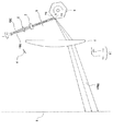
図19は、本発明の画像形成装置の実施形態を示す副走査方向の要部断面図である。図において、符号104は画像形成装置を示す。この画像形成装置104には、パーソナルコンピュータ等の外部機器117からコードデータDcが入力する。このコードデータDcは、装置内のプリンタコントローラ111によって、画像データ(ドットデータ)Diに変換される。この画像データDiは、実施形態1〜4に示した構成を有する光走査ユニット100に入力される。そして、この光走査ユニット100からは、画像データDiに応じて変調された光ビーム103が出射され、この光ビーム103によって感光ドラム101の感光面が主走査方向に走査される。
【0153】
静電潜像担持体(感光体)たる感光ドラム101は、モータ115によって時計廻りに回転させられる。そして、この回転に伴って、感光ドラム101の感光面が光ビーム103に対して、主走査方向と直交する副走査方向に移動する。感光ドラム101の上方には、感光ドラム101の表面を一様に帯電せしめる帯電ローラ102が表面に当接するように設けられている。そして、帯電ローラ102によって帯電された感光ドラム101の表面に、前記光走査ユニット100によって走査される光ビーム103が照射されるようになっている。
【0154】
先に説明したように、光ビーム103は、画像データDiに基づいて変調されており、この光ビーム103を照射することによって感光ドラム101の表面に静電潜像を形成せしめる。この静電潜像は、上記光ビーム103の照射位置よりもさらに感光ドラム101の回転方向の下流側で感光ドラム101に当接するように配設された現像器107によってトナー像として現像される。
【0155】
現像器107によって現像されたトナー像は、感光ドラム101の下方で、感光ドラム101に対向するように配設された転写ローラ108によって被転写材たる用紙112上に転写される。用紙112は感光ドラム101の前方(図15において右側)の用紙カセット109内に収納されているが、手差しでも給紙が可能である。用紙カセット109端部には、給紙ローラ110が配設されており、用紙カセット109内の用紙112を搬送路へ送り込む。
【0156】
以上のようにして、未定着トナー像を転写された用紙112はさらに感光ドラム101後方(図19において左側)の定着器へと搬送される。定着器は内部に定着ヒータ(図示せず)を有する定着ローラ113とこの定着ローラ113に圧接するように配設された加圧ローラ114とで構成されており、転写部から搬送されてきた用紙112を定着ローラ113と加圧ローラ114の圧接部にて加圧しながら加熱することにより用紙112上の未定着トナー像を定着せしめる。更に定着ローラ113の後方には排紙ローラ116が配設されており、定着された用紙112を画像形成装置の外に排出せしめる。
【0157】
図19においては図示していないが、プリントコントローラ111は、先に説明したデータの変換だけでなく、モータ115を始め画像形成装置内の各部や、後述する光走査ユニット内のポリゴンモータなどの制御を行う。
【0158】
[カラー画像形成装置]
図20は本発明の実施態様のカラー画像形成装置の要部概略図である。本実施形態は、光走査装置を4個並べ各々並行して像担持体である感光ドラム面上に画像情報を記録するタンデムタイプのカラー画像形成装置である。図20において、60はカラー画像形成装置、11,12,13,14は各々実施形態1〜4に示したいずれかの構成を有する光走査装置、21,22,23,24は各々像担持体としての感光ドラム、31,32,33,34は各々現像器、51は搬送ベルトである。
【0159】
図20において、カラー画像形成装置60には、パーソナルコンピュータ等の外部機器52からR(レッド)、G(グリーン)、B(ブルー)の各色信号が入力する。これらの色信号は、装置内のプリンタコントローラ53によって、C(シアン),M(マゼンタ),Y(イエロー)、B(ブラック)の各画像データ(ドットデータ)に変換される。これらの画像データは、それぞれ光走査装置11,12,13,14に入力される。そして、これらの光走査装置からは、各画像データに応じて変調された光ビーム41,42,43,44が出射され、これらの光ビームによって感光ドラム21,22,23,24の感光面が主走査方向に走査される。
【0160】
本実施態様におけるカラー画像形成装置は光走査装置(11,12,13,14)を4個並べ、各々がC(シアン),M(マゼンタ),Y(イエロー)、B(ブラック)の各色に対応し、各々平行して感光ドラム21,22,23,24面上に画像信号(画像情報)を記録し、カラー画像を高速に印字するものである。
【0161】
本実施態様におけるカラー画像形成装置は上述の如く4つの光走査装置11,12,13,14により各々の画像データに基づいた光ビームを用いて各色の潜像を各々対応する感光ドラム21,22,23,24面上に形成している。その後、記録材に多重転写して1枚のフルカラー画像を形成している。
【0162】
前記外部機器52としては、例えばCCDセンサを備えたカラー画像読取装置が用いられても良い。この場合には、このカラー画像読取装置と、カラー画像形成装置60とで、カラーデジタル複写機が構成される。
【0163】
[本発明の実施態様]
本発明の様々な例と実施形態が示され説明されたが、当業者であれば、本発明の趣旨と範囲は本明細書内の特定の説明と図に限定されるのではなく、本願特許請求の範囲に全て述べられた様々の修正と変更に及ぶことが理解されるであろう。
【0164】
本発明の実施態様の例を以下に列挙する。
【0165】
[実施態様1]
主走査方向に離間して配置された複数の発光点を有する光源手段と、該光源手段から発せられた複数の光束を被走査面へ向けて偏向する偏向手段とを有するマルチビーム走査装置において、
該光源手段から発せられた複数の光束のうち、主走査方向において該偏向手段の偏向面の中心から最も離れた位置に到達する光束を発光するのを第1の発光点とし、別の光束を発光するのを第2の発光点としたとき、該偏向手段にて偏向可能な角度範囲内にあって、該光束を該被走査面上の有効走査範囲へ向けて偏向する際の有効走査角度範囲よりも、該偏向手段の回転方向上流側に存在する上流側外部角度範囲において、該第2の発光点を最初に発光させたことを特徴とするマルチビーム走査装置。
【0166】
[実施態様2]
前記光源手段から発せられた複数の光束のうち、前記偏向手段の偏向面の中心から最も近い位置に到達する光束を発光する発光点を最初に発光することを特徴とする実施態様1記載のマルチビーム走査装置。
【0167】
[実施態様3]
前記光源手段から発せられた複数の光束のうち、前記偏向手段の偏向面への到達位置が該偏向面の中心から近い光束を発光する発光点より順に発光することを特徴とする実施態様2記載のマルチビーム走査装置。
【0168】
[実施態様4]
主走査方向に離間して配置された複数の発光点を有する光源手段と、該光源手段から発せられた複数の光束を被走査面へ向けて偏向する偏向手段とを有し、該光源手段から発せられた複数の光束は該光源手段と該偏向手段との間でM(M=2n+1、nは整数)回交差するマルチビーム走査装置において、
該偏向手段の回転方向の最も上流側に位置する発光点を第1の発光点とし、別の発光点を第2の発光点としたとき、該偏向手段にて偏向可能な角度範囲内にあって、該光束を該被走査面上の有効走査範囲へ向けて偏向する際の有効走査角度範囲よりも、該偏向手段の回転方向上流側に存在する上流側外部角度範囲において、該第2の発光点を最初に発光させたことを特徴とするマルチビーム走査装置。
【0169】
[実施態様5]
前記偏向手段の回転方向の最も下流側に位置する発光点から最初に発光させたことを特徴とした実施態様4記載のマルチビーム走査装置。
【0170】
[実施態様6]
前記偏向手段の回転方向の最も下流側に位置する発光点から順に発光させたことを特徴とした実施態様5記載のマルチビーム走査装置。
【0171】
[実施態様7]
前記被走査面上の有効走査角度範囲の手前の上流側外部角度範囲において、前記光源手段の発光点から光束を発光することにより、該光束の発光量を調整することを特徴とする実施態様4、5又は6記載のマルチビーム走査装置。
【0172】
[実施態様8]
前記偏向手段で偏向された複数の光束を前記被走査面上に結像させる走査光学系と、前記偏向手段で偏向された複数の光束を受光して前記被走査面上の書き出しのタイミングを検出する同期検出手段とを有し、該走査光学系へ向かう光路と該同期検出手段へ向かう光路とを別光路に設けたことを特徴とする実施態様4乃至7の何れか1項に記載のマルチビーム走査装置。
【0173】
[実施態様9]
前記偏向手段の偏向面の稜線に面取り部を設けたことを特徴とする実施態様4乃至8の何れか1項に記載のマルチビーム走査装置。
【0174】
[実施態様10]
前記偏向手段の回転方向の最も上流側に位置する第1の発光点とは、別の発光点を第3の発光点としたとき、前記被走査面上の有効走査範囲以降の下流側外部角度範囲において、該第3の発光点を最初に発光させたことを特徴とする請求項4乃至9の何れか1項に記載のマルチビーム走査装置。
【0175】
[実施態様11]
主走査方向に離間して配置された複数の発光点を有する光源手段と、該光源手段から発せられた複数の光束を被走査面へ向けて偏向する偏向手段とを有し、該光源手段から発せられた複数の光束は該光源手段と該偏向手段との間でN(N=2n、nは整数)回交差するマルチビーム走査装置において、
該偏向手段の回転方向の最も下流側に位置する発光点を第1の発光点とし、別の発光点を第2の発光点としたとき、該偏向手段にて偏向可能な角度範囲内にあって、該光束を該被走査面上の有効走査角度範囲へ向けて偏向する際の角度範囲よりも該偏向手段の回転方向上流側に存在する上流側外部角度範囲において、該第2の発光点を最初に発光させたことを特徴とするマルチビーム走査装置。
【0176】
[実施態様12]
前記偏向手段の回転方向の最も上流側に位置する発光点から最初に発光させたことを特徴とする実施態様11記載のマルチビーム走査装置。
【0177】
[実施態様13]
前記偏向手段の回転方向の最も上流側に位置する発光点から順に発光させたことを特徴とする実施態様12記載のマルチビーム走査装置。
【0178】
[実施態様14]
前記被走査面上の有効走査範囲の手前の上流側外部角度範囲において、前記光源手段の発光点から光束を発光することにより、該光束の発光量を調整することを特徴とする実施態様11、12又は13記載のマルチビーム走査装置。
【0179】
[実施態様15]
前記偏向手段で偏向された複数の光束を前記被走査面上に結像させる走査光学系と、前記偏向手段で偏向された複数の光束を受光して前記被走査面上の書き出しのタイミングを検出する同期検出手段とを有し、該走査光学系へ向かう光路と該同期検出手段へ向かう光路とを別光路に設けたことを特徴とする実施態様11乃至14の何れか1項に記載のマルチビーム走査装置。
【0180】
[実施態様16]
前記偏向手段の偏向面の稜線に面取り部を設けたことを特徴とする実施態様11乃至15の何れか1項に記載のマルチビーム走査装置。
【0181】
[実施態様17]
前記偏向手段の回転方向の最も下流側に位置する第1の発光点とは、別の発光点を第3の発光点としたとき、前記被走査面上の有効走査範囲以降の下流側外部角度範囲において、該第3の発光点を最初に発光させたことを特徴とする請求項11乃至16の何れか1項に記載のマルチビーム走査装置。
【0182】
[実施態様18]
主走査方向に離間して配置された複数の発光点を有する光源手段と、該光源手段から発せられた複数の光束を被走査面へ向けて偏向する偏向手段とを有するマルチビーム走査装置において、
該光源手段から発せられた複数の光束のうち、主走査方向において該偏向手段の偏向面に最初に入射する光束を発光する発光点を他の発光点よりも先に発光させていることを特徴とするマルチビーム走査装置。
【0183】
[実施態様19]
実施態様1乃至18の何れか1項に記載のマルチビーム走査装置と、前記被走査面に配置された感光体と、前記マルチビーム走査装置で走査された光ビームによって前記感光体上に形成された静電潜像をトナー像として現像する現像器と、現像されたトナー像を被転写材に転写する転写器と、転写されたトナー像を被転写材に定着させる定着器とを有することを特徴とする画像形成装置。
【0184】
[実施態様20]
実施態様1乃至18の何れか1項に記載のマルチビーム走査装置と、外部機器から入力したコードデータを画像信号に変換して前記マルチビーム走査装置に入力せしめるプリンタコントローラとを有していることを特徴とする画像形成装置。
【0185】
[実施態様21]
各々が実施態様1乃至18のいずれか1項に記載のマルチビーム走査装置の被走査面に配置され、互いに異なった色の画像を形成する複数の像担持体とを有することを特徴とするカラー画像形成装置。
【0186】
[実施態様22]
外部機器から入力した色信号を異なった色の画像データに変換して各々のマルチビーム走査装置に入力せしめるプリンタコントローラを有していることを特徴とする実施態様21記載のカラー画像形成装置。
【0187】
【発明の効果】
本発明によれば前述の如く光源手段から発せられた複数の光束のうち、偏向手段の偏向面の中心から最も近い位置に到達する光束を発光する発光点を最初に発光することにより、偏向面を有効的に使用することができ、かつ偏向手段の小型化を図ることができ、これにより装置全体の小型化が図れると共に偏向手段やモーター等を簡易に構成することができるマルチビーム走査装置を達成することができる。
【図面の簡単な説明】
【図1】本発明の実施形態1の主走査断面図
【図2】本発明の実施形態1の要部概要図
【図3】本発明の実施形態1における同期検出手段を説明する図
【図4】本発明の実施形態1における光源手段の要部概要図
【図5】本発明の実施形態1の要部概要図
【図6A】本発明の実施形態1における偏向の様子を説明する図
【図6B】本発明の実施形態1における偏向の様子を説明する図
【図6C】本発明の実施形態1における偏向の様子を説明する図
【図6D】本発明の実施形態1における偏向の様子を説明する図
【図6E】本発明の実施形態1における偏向の様子を説明する図
【図7】本発明の実施形態2の主走査断面図
【図8】本発明の実施形態2の要部概要図
【図9】本発明の実施形態2の要部概要図
【図10】本発明の実施形態3の主走査断面図
【図11】本発明の実施形態4の主走査断面図
【図12A】本発明の実施形態4における偏向の様子を説明する図
【図12B】本発明の実施形態4における偏向の様子を説明する図
【図13】本発明の実施形態5の主走査断面図
【図14】本発明の実施形態5の要部概要図
【図15A】本発明の実施形態5における偏向の様子を説明する図
【図15B】本発明の実施形態5における偏向の様子を説明する図
【図16】本発明の実施形態6の主走査断面図
【図17A】本発明の実施形態6の要部概要図
【図17B】本発明の実施形態6の要部概要図
【図17C】本発明の実施形態6の要部概要図
【図18】本発明の実施形態7の主走査断面図
【図19】本発明の画像形成装置の実施形態を示す副走査断面図
【図20】本発明の実施態様のカラー画像形成装置の要部概略図
【図21】従来のマルチビーム走査装置における斜視図
【符号の説明】
1、71、81 光源手段(半導体レーザアレイ)
1a、1b,1c,1d 発光点
2 集光レンズ系(コリメータ−レンズ)
3 レンズ系(シリンドリカルレンズ)
4 開口絞り
5 偏向手段(ポリゴンミラー)
7 走査光学系
8 被走査面(感光ドラム面)
9 BDミラー
10 同期検出手段
10a BDスリット
10b BDセンサー
72 BDレンズ
73 走査位置検出用光学系
74 走査位置検出手段
74a スリット
74b センサー
11、12、13、14 光走査装置
21、22、23、24 像担持体(感光ドラム)
31、32、33、34 現像器
41 搬送ベルト
51 マルチビームレーザー
52 外部機器
53 プリンタコントローラ
60 カラー画像形成装置
100 マルチビーム走査装置
101 感光体
102 帯電ローラ
103 光ビーム
104 画像形成装置
107 現像装置
108 転写ローラ
109 用紙カセット
110 給紙ローラ
112 転写材(用紙)
113 定着ローラ
114 加圧ローラ
116 排紙ローラ
117 外部機器[0001]
TECHNICAL FIELD OF THE INVENTION
The present invention relates to a multi-beam scanning apparatus, and more particularly, to reflect and deflect a light beam emitted from a light source means by a polygon mirror as a deflecting means, and to optically scan a surface to be scanned through a scanning optical system to record image information. For example, the present invention is suitable for an image forming apparatus such as a laser beam printer having an electrophotographic process, a digital copying machine, and a multifunction printer (multifunction printer).
[0002]
In particular, in a multi-beam scanning apparatus which achieves high-speed and high-definition by simultaneously scanning a plurality of light beams, the size of the entire apparatus is reduced by efficiently using a deflecting means such as a polygon mirror.
[0003]
[Prior art]
FIG. 21 is a schematic view of a main part of a conventional multi-beam scanning device.
[0004]
In the figure, two light fluxes which are light-modulated and emitted from the light source means 91 in accordance with image information are converted into substantially parallel light fluxes by a
[0005]
At this time, in order to adjust the timing of the scanning start position on the
[0006]
In order to obtain a high-quality image in this type of multi-beam scanning apparatus, the light emission amount of each light beam is adjusted (hereinafter, also referred to as "auto power control (APC)") before starting to write a scanning line, so that it is on the surface of the photosensitive drum. The amount of light radiated to is always constant.
[0007]
A multi-beam scanning device for detecting the synchronization (BD detection) and adjusting the light quantity of the plurality of light beams emitted from the light source means (APC); A device has been proposed.
[0008]
[Problems to be solved by the invention]
However, these conventional multi-beam scanning devices do not mention the order of light emission of the light source means, and cannot use the optical deflector (polygon mirror) effectively. Therefore, it is necessary to use a large optical deflector.
[0009]
Further, when the end of the deflecting surface of the optical deflector is chamfered, the light beam incident on the chamfered portion reaches the surface of the photosensitive drum, which may cause a problem of ghost.
[0010]
SUMMARY OF THE INVENTION It is an object of the present invention to provide a multi-beam scanning device capable of reducing the size of a deflection unit. Another object of the present invention is to provide a multi-beam scanning apparatus which can always obtain a good image without ghost light.
[0011]
[Means for Solving the Problems]
The multi-beam scanning device according to the present invention includes:
In a multi-beam scanning apparatus having a light source means having a plurality of light emitting points spaced apart in the main scanning direction and a deflecting means for deflecting a plurality of light beams emitted from the light source means toward a surface to be scanned,
Among the plurality of light beams emitted from the light source means, a light ray that reaches a position farthest from the center of the deflection surface of the deflection means in the main scanning direction is emitted as a first light emitting point, and another light flux is emitted. Assuming that the light is emitted as a second light emitting point, the effective scanning angle is within an angle range that can be deflected by the deflecting means, and is used to deflect the light beam toward an effective scanning range on the surface to be scanned. The second light-emitting point is first emitted in an upstream external angle range that is located on the upstream side in the rotation direction of the deflecting means than the range.
[0012]
BEST MODE FOR CARRYING OUT THE INVENTION
(Embodiment 1)
FIG. 1 is a cross-sectional view (main scanning cross-sectional view) of a main portion of the multi-beam scanning device according to the first embodiment of the present invention in the main scanning direction.
[0013]
Here, the main scanning direction indicates a direction perpendicular to the rotation axis of the deflecting means and the optical axis of the scanning optical element (the direction in which the light beam is reflected and deflected (deflection scanning) by the deflecting means). 3 shows a direction parallel to the rotation axis. The main scanning section indicates a plane parallel to the main scanning direction and including the optical axis of the scanning optical system. The sub-scanning section indicates a section perpendicular to the main scanning section.
[0014]
In FIG. 1,
[0015]
[0016]
Incidentally, each element such as the
[0017]
[0018]
Reference numeral 7 denotes a scanning optical system having imaging performance and fθ characteristics, which is constituted by a single scanning lens, and on which the two light beams BMa and BMb deflected by the
[0019]
[0020]
[0021]
[0022]
Each element such as the
[0023]
In the present embodiment, two light beams BMa and BMb, which are light-modulated and emitted from the light source means 1 in accordance with image information, are converted into substantially parallel light beams by the
[0024]
At this time, in order to adjust the timing of the scanning start position on the
[0025]
FIG. 2 is a schematic diagram of a main part of the multi-beam scanning device according to the first embodiment of the present invention. In the figure, the same elements as those shown in FIG. 1 are denoted by the same reference numerals.
[0026]
In the figure, the range over which the light beam emitted from the light source means 1 can be deflected on the
[0027]
(Equation 1)
In the present embodiment, the number of surfaces C of the
[0029]
(Equation 2)
Range.
[0031]
In the case of a scanning optical system, the deflection angle (angle of view) and the scanning position have a one-to-one correspondence. Therefore, when specifying the range, the deflection angle may be used, or the scanning position may be used.
[0032]
At the center of the above-mentioned "deflectable angle range" 8c, there is usually an "effective scanning angle range" 8b, and the "effective scanning range" 8a corresponding to the scanning position is on the
[0033]
The angle at which the light beam is deflected by the
[0034]
In the present embodiment, as will be described later, of the two light beams BMa and BMb emitted from the
[0035]
FIG. 3 is a diagram for explaining the state of light detection in the
[0036]
FIG. 4 is a diagram showing the arrangement of two light emitting points 1a and 1b of the light source means 1. In the multi-beam scanning device according to the present embodiment, the
[0037]
FIG. 5 is a schematic diagram of a main part of the multi-beam scanning device according to the present embodiment in the main scanning direction. In the figure, the same elements as those shown in FIG. 1 are denoted by the same reference numerals. FIG. 1 schematically shows how a light beam emitted from the light source means 1 is reflected and deflected by the
[0038]
In the multi-beam scanning device according to the present embodiment, the two light emitting points 1a and 1b are arranged apart from each other in the main scanning direction, and the two light beams BMa and BMb emitted from the respective light emitting points 1a and 1b are deflecting surfaces. 5A, a position distant in the main scanning direction is reached. Therefore, when the two light beams BMa and BMb emitted from the light source means 1 are deflected by the deflecting
[0039]
When the light beam BMb kicked by the
[0040]
However, if the deflecting
[0041]
Thus, in the present embodiment, the above problem is solved by using the
[0042]
That is, of the two light beams emitted from the light source means 1, the light emitting point that emits the light beam that first enters the
[0043]
Specifically, of the two light beams BMa and BMb reaching the deflecting
[0044]
Here, the two light beams BMa and BMb have different positions at which the synchronization is detected, but this can be easily dealt with by providing the positions of the
[0045]
FIGS. 6A to 6E are diagrams schematically showing the state of two light beams BMa and BMb reaching the
[0046]
FIG. 6A is a view showing a state in which a light beam BMa from a light emitting point (second light emitting point) 1a is deflected toward a synchronization detecting means (not shown), and the light beam BMa is reflected and deflected by the deflecting
[0047]
FIG. 6B is a diagram showing a state in which the light beam BMb is deflected toward the synchronization detecting means (not shown), and the light beam BMb is also reflected and deflected by the deflecting
[0048]
FIG. 6C is a diagram showing how each light beam is deflected into the effective scanning range on the surface to be scanned, and both light beams BMa and BMb have reached near the center of the
[0049]
FIG. 6D is a diagram illustrating a state where each light beam is deflected toward a position beyond the effective scanning range on the surface to be scanned. This time, the light beam BMa reaches a position distant from the center of the deflecting
[0050]
FIG. 6E is a diagram showing a state immediately after FIG. 6D. The light beam BMa straddles the end of the deflecting
[0051]
When FIG. 6A to FIG. 6E are arranged in chronological order, FIG. 6A → FIG. 6B → FIG. 6C → FIG. 6D → FIG. 6E, it can be seen that two light beams BMa and BMb are moving on the
[0052]
In FIG. 6A, only the light beam BMa can reflect and deflect the entire light beam. However, if a short time elapses and the state shown in FIG. 6B is reached, the light beam BMb can also reflect and deflect the entire light beam.
[0053]
In the present embodiment, the synchronization detection is performed when all the light beams can be reflected and deflected by the
[0054]
Further, in the present embodiment, the two light beams BMa and BMb intersect at the
[0055]
Therefore, in this embodiment, when the light emitting point located on the most upstream side in the rotation direction of the
[0056]
In other words, by using the effects of the present embodiment, it is possible to provide a multi-beam scanning apparatus having a simple configuration capable of obtaining a compact and always good image.
[0057]
As described above, in the present embodiment, as described above, the light emitting point (second light emitting point) 1a located on the most downstream side in the rotation direction of the
[0058]
In the present embodiment, the BD light flux is present in the upstream external angle range 8d, but the BD light flux may be present in the downstream external angle range 8e.
[0059]
(Embodiment 2)
FIG. 7 is a main scanning sectional view of the multi-beam scanning device according to the second embodiment of the present invention. In the figure, the same elements as those shown in FIG. 1 are denoted by the same reference numerals.
[0060]
This embodiment is different from the first embodiment in that the light source means 1 has four light emitting points. Other configurations and optical functions are substantially the same as those of the first embodiment, and thus, similar effects are obtained.
[0061]
That is, in FIG. 1,
[0062]
FIG. 8 is a diagram schematically showing the state of four light beams BMa, BMb, BMc, and BMd from the light source means 1 reaching the
[0063]
In the present embodiment, four light beams BMa (solid line), BMb (small broken line), BMc (two-dot chain line), and BMd (large broken line) emitted from the light source means 1 intersect at the
[0064]
The diameter of the inscribed circle of the
[0065]
In the present embodiment, the four light beams BMa, BMb, BMc, and BMd reach different positions on the
[0066]
Here, the spread Tm (mm) of the four light beams BMa, BMb, BMc, and BMd reaching the
[0067]
The spread Tm of the four light beams from the light beam width Wm (mm) in the main scanning direction, the variation ΔTm (mm) of the adjacent light beams, the number of beams n (number), and the angle of incidence γ (rad) of the light beams on the
[0068]
[Equation 3]
The four light beams BMa, BMb, BMc and BMd emitted from the respective light emitting points 1a, 1b, 1c and 1d are not parallel to each other but have a certain angle α. In the main scanning direction after passing through the
[0070]
(Equation 4)
When the light exits the
[0072]
At this time, the distance Lap (mm) from the position closest to the deflecting
[0073]
Here, the variation ΔTm (mm) between adjacent light beams is expressed by the following equation based on the distance Lap (mm) between the
[0074]
(Equation 5)
![]()
From equations (3) and (5), the spread Tm (mm) of the four light beams is expressed by the following equation.
[0076]
(Equation 6)
Or, from the formulas (4) and (5), the variation ΔTm (mm) between adjacent light fluxes is
[0078]
(Equation 7)
From the expressions (3) and (7), the spread Tm (mm) of the four light beams is expressed by the following expression.
[0080]
(Equation 8)
In other words, in a multi-beam scanning device having four light emitting points spaced apart in the main scanning direction, the spread Tm (mm) of the four light beams on the
[0082]
Therefore, in the present embodiment, the light beam BMd emitted from the light emitting point (first light emitting point) 1d arranged on the most upstream side in the rotation direction A of the
[0083]
That is, if a light beam other than the light beam reaching the position farthest from the center of the
[0084]
As a result, the deflecting
[0085]
In the present embodiment, four light beams are scanned at one time. However, the present invention is not limited to this, and the present invention is applicable to a multi-beam scanning apparatus that handles more beams, such as 8, 16, 32,. Can be obtained at least the same effect.
[0086]
(Embodiment 3)
FIG. 10 is a main scanning cross-sectional view of the multi-beam scanning device according to the third embodiment of the present invention. In the figure, the same elements as those shown in FIG. 1 are denoted by the same reference numerals.
[0087]
The present embodiment is different from the above-described first embodiment in that a light beam (BD light beam) deflected by the
[0088]
That is, in the figure,
[0089]
As in the present embodiment, another
[0090]
Further, by arranging the BD slit 10a of the synchronization detecting means 10 on the optical axis of the
[0091]
As described above, the merit of using another
[0092]
However, in comparison with the multi-beam scanning device that guides the light beam that has passed through the scanning lens 7 to the
[0093]
Therefore, in the present embodiment, as in the first embodiment, this problem is solved by appropriately setting the order of the light-emitting points that emit light beams for synchronization detection.
[0094]
That is, in this embodiment, the two light beams BMa and BMb emitted from the light source means 1 intersect at the
[0095]
Accordingly, even in a multi-beam scanning apparatus in which the optical path toward the scanning lens 7 and the optical path toward the
[0096]
(Embodiment 4)
FIG. 11 is a main scanning cross-sectional view of the multi-beam scanning device according to the fourth embodiment of the present invention. In the figure, the same elements as those shown in FIG. 1 are denoted by the same reference numerals.
[0097]
This embodiment is different from the first embodiment in that the rotation direction of the
[0098]
That is, in the multi-beam scanning device of the present embodiment, the light source means 1 has two light emitting points 1a and 1b separated in the main scanning direction, and two light beams emitted from the respective light emitting points 1a and 1b. After passing through the
[0099]
The
[0100]
Here, when the
[0101]
When the light beam from the light source means 1 is deflected to the negative side θ (−) by the
[0102]
In the multi-beam scanning apparatus in which the
[0103]
Therefore, in the present embodiment, stable synchronization detection without kicking is performed by devising the order of light emission when performing synchronization detection.
[0104]
FIGS. 12A and 12B are diagrams schematically showing the state of two light beams BMa and BMb reaching the
[0105]
FIG. 12A is a view showing a state in which the light beam BMb (broken line) is deflected toward the synchronization detecting means (not shown). In the light beam BMb (broken line), all the light beams are reflected and deflected by the deflecting
[0106]
FIG. 12B is a view showing a state in which the light beam BMa (solid line) is deflected toward the synchronization detecting means after a short time has elapsed from FIG. 12A. The light beam BMb (dashed line) is also reflected and deflected by the deflecting
[0107]
In this embodiment, the arrangement of the light emitting points is the same as that of the third embodiment. However, since the rotation direction A of the
[0108]
Accordingly, the deflecting
[0109]
(Embodiment 5)
FIG. 13 is a main scanning sectional view of the multi-beam scanning device according to the fifth embodiment of the present invention. In the figure, the same elements as those shown in FIG. 1 are denoted by the same reference numerals.
[0110]
The present embodiment is different from the above-described first embodiment in that a chamfered
[0111]
That is, the two light beams BMa and BMb emitted from the two light emitting points 1a and 1b of the
[0112]
The light source means 1 in this embodiment is a monolithic semiconductor laser array, and measures the amount of light emitted from each of the two light emitting points 1a and 1b by a measuring device provided inside the laser element. Then, based on the measurement result from the measuring instrument, the light emission amount is adjusted to a desired value.
[0113]
An end of the deflecting
[0114]
In recent years, the angle of view of the scanning lens 7 has been increased with the miniaturization of the multi-beam scanning device, and there is no room for the
[0115]
APC is generally performed immediately before synchronization detection. When the light is deflected by the deflecting
[0116]
However, if the chamfered
[0117]
FIG. 14 is a main scanning sectional view for explaining ghost light BMgh generated in the chamfered
[0118]
The light beam emitted from the light source means 1 is applied to the chamfered
[0119]
Therefore, in the present embodiment, the ghost light BMgh generated in the chamfered
[0120]
FIGS. 15A and 15B are diagrams schematically showing the state of two light beams BMa and BMb reaching the
[0121]
As shown in FIG. 15A, of the two light beams BMa and BMb emitted from the light source means 1, the light emitting point (the first light emitting point) emits the light beam BMa reaching the position closest to the center of the
[0122]
In this embodiment, the light fluxes BMa and BMb emitted from the two light emitting points 1a and 1b of the light source means 1 intersect the light source means 1 and the
[0123]
Thus, it is possible to provide a multi-beam scanning apparatus that can always obtain a good image while avoiding ghost while using the small
[0124]
When the order of light emission is arranged in time series, first, the light emitting point 1a that emits the light beam BMa is made to emit light, APC is performed, and then the light is turned off. Next, APC is performed by causing the light emitting point 1b that emits the light beam BMb to emit light, and synchronization detection is directly performed without turning off the light. Finally, the light emitting point 1a that emits the light beam BMa is re-emitted to perform synchronization detection.
[0125]
As described above, the synchronization is detected after the APC is performed. Since the light beam is not kicked by the deflecting
[0126]
In the present embodiment, the case where the number of light emitting points is two has been described as an example. However, the present invention is not limited to this. For example, even when the number of light emitting points is increased to four, eight, sixteen. The effects of the present invention can be obtained at the same level or more.
[0127]
Further, in the present embodiment, the ghost light beam generated in the chamfered
[0128]
(Embodiment 6)
FIG. 16 is a cross-sectional view (main scanning cross-sectional view) of a main part of the multi-beam scanning device according to the sixth embodiment of the present invention in the main scanning direction. In the figure, the same elements as those shown in FIG. 1 are denoted by the same reference numerals.
[0129]
This embodiment is different from the above-described first embodiment in that three light emitting points of the light source means 81 are used, and three light beams BMa, BMb, and BMc emitted from the light emitting points 1a, 1b, and 1c are used as light sources. The point that the light is incident on the deflecting
[0130]
That is, in FIG. 1,
[0131]
In the present embodiment, the three light beams BMa, BMb, and BMc emitted from the respective light emitting points 1a, 1b, and 1c enter the
[0132]
FIGS. 17A to 17C are diagrams schematically showing the states of three light beams BMa, BMb, and BMc reaching the
[0133]
FIG. 17A is a diagram showing a state in which a light beam BMa (solid line) emitted for the APC at the light emitting point (third light emitting point) 1a is reflected and deflected by the deflecting
[0134]
FIG. 17B is a diagram showing a state in which a light beam BMb (broken line) emitted for APC at the light emitting point (second light emitting point) 1b is reflected and deflected by the deflecting
[0135]
FIG. 17C is a diagram showing a state in which a light flux BMc (two-dot chain line) emitted for the APC at the light emitting point (first light emitting point) 1c is reflected and deflected by the deflecting
[0136]
In the present embodiment, since the three light beams BMa, BMb, and BMc are incident on the
[0137]
Therefore, in the present embodiment, first, the light emitting point (third light emitting point) 1a that emits the light flux BMa located at the most upstream side in the rotation direction A of the
[0138]
Also in the synchronization detection, first, the light emitting point 1a that emits the light beam BMa located at the most upstream side in the rotation direction A of the
[0139]
When these are arranged in time series, first, the light emitting point 1a that emits the light beam BMa is caused to emit light, APC is performed, synchronization detection is performed as it is, and the light is turned off. Next, APC is performed by causing the light emitting point 1b that emits the light beam BMb to emit light, synchronization detection is performed as it is, and the light is turned off. Finally, the light emitting point 1c that emits the light beam BMc is emitted, APC is performed, synchronization detection is performed, and the light is turned off.
[0140]
By appropriately setting the order in which light emission is started among a plurality of light emission points, the
[0141]
In the present embodiment, an optical path toward the scanning optical system 7 and an optical path toward the
[0142]
(Embodiment 7)
FIG. 18 is a main scanning sectional view of the multi-beam scanning device according to the seventh embodiment of the present invention. In the figure, the same elements as those shown in FIG. 1 are denoted by the same reference numerals.
[0143]
This embodiment is different from the first embodiment in that the scanning position detecting means 74 is provided outside the effective scanning range on the scanning end side, and the scanning position detecting means 74 is provided between the
[0144]
That is, in the drawing,
[0145]
The present embodiment is a multi-beam scanning device of a type in which M = 2 × n + 1 (n is an integer) crossing once between the light source means 1 and the deflecting
[0146]
Therefore, before the start of scanning, the light emitting point (second light emitting point) 1a located on the most downstream side in the rotation direction A of the
[0147]
More specifically, the light emitting point 1a that emits the light beam BMa emits light, turns off the light after performing APC, and then emits the light emitting point 1b that emits the light beam BMb located on the upstream side in the rotation direction A of the
[0148]
Further, even after the scanning is completed, the light emitting point (third light emitting point) 1a located on the downstream side in the rotation direction A of the
[0149]
As described above, in the case of emitting a plurality of light beams immediately before the start of scanning or the case of emitting a plurality of light beams immediately after the end of scanning, the
[0150]
Further, when a plurality of light beams are emitted immediately before and immediately after the effective scanning range on the
[0151]
In the present embodiment, an odd number (M = 2 × n + 1) times intersecting once between the light source means 1 and the deflecting
[0152]
[Image forming apparatus]
FIG. 19 is a cross-sectional view of a main part of the image forming apparatus according to the embodiment of the present invention in the sub-scanning direction. In the figure,
[0153]
The
[0154]
As described above, the
[0155]
The toner image developed by the developing
[0156]
As described above, the
[0157]
Although not shown in FIG. 19, the
[0158]
[Color image forming apparatus]
FIG. 20 is a schematic view of a main part of a color image forming apparatus according to an embodiment of the present invention. The present embodiment is a tandem type color image forming apparatus in which four optical scanning devices are arranged and image information is recorded in parallel on the surface of a photosensitive drum as an image carrier. 20,
[0159]
In FIG. 20, R (red), G (green), and B (blue) color signals are input to the color
[0160]
The color image forming apparatus according to the present embodiment includes four optical scanning devices (11, 12, 13, 14), each of which has a color of C (cyan), M (magenta), Y (yellow), and B (black). Correspondingly, an image signal (image information) is recorded on the
[0161]
As described above, the color image forming apparatus according to the present embodiment uses the four
[0162]
As the
[0163]
[Embodiments of the present invention]
Although various examples and embodiments of the present invention have been shown and described, those skilled in the art will recognize that the spirit and scope of the present invention is not limited to the specific description and figures herein, but rather is limited to the present patent application. It will be understood that various modifications and changes are set forth which are all set forth in the following claims.
[0164]
Examples of embodiments of the present invention are listed below.
[0165]
[Embodiment 1]
In a multi-beam scanning apparatus having a light source means having a plurality of light emitting points spaced apart in the main scanning direction and a deflecting means for deflecting a plurality of light beams emitted from the light source means toward a surface to be scanned,
Among the plurality of light beams emitted from the light source means, the first light emitting point emits a light beam that reaches a position farthest from the center of the deflection surface of the deflection means in the main scanning direction, and another light beam is emitted. Assuming that the light is emitted as a second light emitting point, the effective scanning angle is within an angle range that can be deflected by the deflecting means, and is used to deflect the light beam toward an effective scanning range on the surface to be scanned. A multi-beam scanning device, wherein the second light emitting point is first emitted in an upstream external angle range existing on the upstream side in the rotation direction of the deflection unit from the range.
[0166]
[Embodiment 2]
The light emitting point which emits a light beam that emits a light beam that reaches a position closest to the center of the deflection surface of the deflection unit among a plurality of light beams emitted from the light source unit is emitted first. Beam scanning device.
[0167]
[Embodiment 3]
3. The light emitting device according to
[0168]
[Embodiment 4]
Light source means having a plurality of light emitting points spaced apart in the main scanning direction, and deflecting means for deflecting a plurality of luminous fluxes emitted from the light source means toward a surface to be scanned, from the light source means In the multi-beam scanning device, the emitted light beams cross M (M = 2n + 1, n is an integer) times between the light source means and the deflection means,
When a light emitting point located on the most upstream side in the rotation direction of the deflecting means is a first light emitting point and another light emitting point is a second light emitting point, the light emitting point falls within an angle range which can be deflected by the deflecting means. In the upstream external angle range existing on the upstream side in the rotation direction of the deflecting unit, the second external angle range is larger than the effective scanning angle range when the light beam is deflected toward the effective scanning range on the surface to be scanned. A multi-beam scanning device characterized in that a light emitting point emits light first.
[0169]
[Embodiment 5]
The multi-beam scanning apparatus according to the fourth embodiment, wherein light is emitted first from a light emitting point located on the most downstream side in the rotation direction of the deflecting means.
[0170]
[Embodiment 6]
The multi-beam scanning apparatus according to
[0171]
[Embodiment 7]
A fourth embodiment of the present invention is characterized in that the light emission amount of the light beam is adjusted by emitting the light beam from the light emitting point of the light source means in the upstream external angle range before the effective scanning angle range on the surface to be scanned. 7. The multi-beam scanning device according to 5 or 6.
[0172]
[Embodiment 8]
A scanning optical system that forms a plurality of light beams deflected by the deflecting means on the surface to be scanned, and receives a plurality of light beams deflected by the deflecting means to detect a writing start timing on the surface to be scanned The multipath according to any one of
[0173]
[Embodiment 9]
The multi-beam scanning apparatus according to any one of
[0174]
[Embodiment 10]
The first light emitting point located on the most upstream side in the rotation direction of the deflecting means is a downstream external angle after the effective scanning range on the surface to be scanned, when another light emitting point is a third light emitting point. The multi-beam scanning device according to any one of
[0175]
[Embodiment 11]
Light source means having a plurality of light emitting points spaced apart in the main scanning direction, and deflecting means for deflecting a plurality of luminous fluxes emitted from the light source means toward a surface to be scanned, from the light source means In the multi-beam scanning device, the emitted plural light beams intersect N times (N = 2n, n is an integer) between the light source means and the deflection means,
When the light-emitting point located at the most downstream side in the rotation direction of the deflecting means is a first light-emitting point and another light-emitting point is a second light-emitting point, the light-emitting point falls within an angle range that can be deflected by the deflection means. The second light emitting point is located in an upstream external angle range that is located on the upstream side in the rotation direction of the deflecting unit with respect to the angle range when the light beam is deflected toward the effective scanning angle range on the surface to be scanned. A multi-beam scanning device characterized by emitting light for the first time.
[0176]
[Embodiment 12]
The multi-beam scanning apparatus according to
[0177]
[Embodiment 13]
13. The multi-beam scanning apparatus according to
[0178]
[Embodiment 14]
In the eleventh embodiment, a light beam is emitted from a light emitting point of the light source means in an upstream external angle range before an effective scanning range on the surface to be scanned, thereby adjusting a light emission amount of the light beam. 14. The multi-beam scanning device according to 12 or 13.
[0179]
[Embodiment 15]
A scanning optical system for forming an image of the plurality of light beams deflected by the deflecting means on the surface to be scanned, and detecting timing of starting writing on the surface to be scanned by receiving the plurality of light beams deflected by the deflecting means 15. The multi-purpose optical system according to
[0180]
[Embodiment 16]
The multi-beam scanning apparatus according to any one of
[0181]
[Embodiment 17]
The first light emitting point located on the most downstream side in the rotation direction of the deflecting means is a downstream external angle after the effective scanning range on the surface to be scanned, when another light emitting point is a third light emitting point. The multi-beam scanning device according to any one of
[0182]
[Embodiment 18]
In a multi-beam scanning apparatus having a light source means having a plurality of light emitting points spaced apart in the main scanning direction and a deflecting means for deflecting a plurality of light beams emitted from the light source means toward a surface to be scanned,
A light emitting point for emitting a light flux that first enters the deflection surface of the deflection means in the main scanning direction among a plurality of light beams emitted from the light source means is emitted before other light emitting points. Multi-beam scanning device.
[0183]
[Embodiment 19]
19. The multi-beam scanning device according to any one of
[0184]
[Embodiment 20]
19. The multi-beam scanning device according to any one of the first to eighteenth embodiments, and a printer controller that converts code data input from an external device into an image signal and inputs the image signal to the multi-beam scanning device. An image forming apparatus comprising:
[0185]
[Embodiment 21]
19. A color, comprising: a plurality of image carriers each arranged on a surface to be scanned of the multi-beam scanning device according to any one of the first to eighteenth embodiments and forming images of different colors. Image forming device.
[0186]
[Embodiment 22]
The color image forming apparatus according to the twenty-first embodiment, further comprising a printer controller for converting a color signal input from an external device into image data of a different color and inputting the data to each multi-beam scanning device.
[0187]
【The invention's effect】
According to the present invention, as described above, among the plurality of light beams emitted from the light source means, the light emitting point that emits the light beam that reaches the position closest to the center of the deflecting surface of the deflecting means first emits light. Can be used effectively, and the size of the deflecting means can be reduced, thereby making it possible to reduce the size of the entire apparatus and to simplify the configuration of the deflecting means and the motor. Can be achieved.
[Brief description of the drawings]
FIG. 1 is a main scanning sectional view of a first embodiment of the present invention.
FIG. 2 is a schematic diagram of a main part of the first embodiment of the present invention.
FIG. 3 is a diagram illustrating a synchronization detecting unit according to the first embodiment of the present invention.
FIG. 4 is a schematic diagram of a main part of a light source unit according to the first embodiment of the present invention.
FIG. 5 is a schematic diagram of a main part of the first embodiment of the present invention.
FIG. 6A is a diagram illustrating a state of deflection in the first embodiment of the present invention.
FIG. 6B is a diagram illustrating a state of deflection in the first embodiment of the present invention.
FIG. 6C is a diagram illustrating a state of deflection in the first embodiment of the present invention.
FIG. 6D is a diagram illustrating a state of deflection in the first embodiment of the present invention.
FIG. 6E is a diagram illustrating a state of deflection in the first embodiment of the present invention.
FIG. 7 is a main scanning cross-sectional view according to a second embodiment of the present invention.
FIG. 8 is a schematic diagram of a main part of a second embodiment of the present invention.
FIG. 9 is a schematic diagram of a main part of a second embodiment of the present invention.
FIG. 10 is a main scanning sectional view according to a third embodiment of the present invention.
FIG. 11 is a main scanning cross-sectional view according to a fourth embodiment of the present invention.
FIG. 12A is a diagram illustrating a state of deflection in a fourth embodiment of the present invention.
FIG. 12B is a diagram illustrating a state of deflection in the fourth embodiment of the present invention.
FIG. 13 is a main scanning sectional view according to a fifth embodiment of the present invention.
FIG. 14 is a schematic diagram of a main part of a fifth embodiment of the present invention.
FIG. 15A is a diagram illustrating a state of deflection in the fifth embodiment of the present invention.
FIG. 15B is a diagram illustrating a state of deflection in the fifth embodiment of the present invention.
FIG. 16 is a main scanning cross-sectional view according to a sixth embodiment of the present invention.
FIG. 17A is a schematic diagram of a main part of a sixth embodiment of the present invention.
FIG. 17B is a schematic diagram of a main part of the sixth embodiment of the present invention.
FIG. 17C is a schematic diagram of a main part of the sixth embodiment of the present invention.
FIG. 18 is a main scanning sectional view according to a seventh embodiment of the present invention.
FIG. 19 is a sub-scan sectional view illustrating an embodiment of the image forming apparatus of the present invention.
FIG. 20 is a schematic view of a main part of a color image forming apparatus according to an embodiment of the present invention.
FIG. 21 is a perspective view of a conventional multi-beam scanning device.
[Explanation of symbols]
1, 71, 81 Light source means (semiconductor laser array)
1a, 1b, 1c, 1d Light emitting point
2 Condensing lens system (collimator-lens)
3 lens system (cylindrical lens)
4 Aperture stop
5. Deflection means (polygon mirror)
7 Scanning optical system
8 Scanned surface (photosensitive drum surface)
9 BD mirror
10 Synchronization detection means
10a BD slit
10b BD sensor
72 BD lens
73 Scanning position detection optical system
74 scanning position detecting means
74a slit
74b sensor
11, 12, 13, 14 optical scanning device
21, 22, 23, 24 Image carrier (photosensitive drum)
31, 32, 33, 34 Developer
41 Conveyor belt
51 Multi-beam laser
52 External equipment
53 Printer Controller
60 color image forming apparatus
100 multi-beam scanner
101 Photoconductor
102 Charging roller
103 light beam
104 Image forming apparatus
107 Developing device
108 transfer roller
109 Paper cassette
110 Paper feed roller
112 Transfer material (paper)
113 Fixing roller
114 pressure roller
116 Paper ejection roller
117 External device
Claims (1)
該光源手段から発せられた複数の光束のうち、主走査方向において該偏向手段の偏向面の中心から最も離れた位置に到達する光束を発光するのを第1の発光点とし、別の光束を発光するのを第2の発光点としたとき、該偏向手段にて偏向可能な角度範囲内にあって、該光束を該被走査面上の有効走査範囲へ向けて偏向する際の有効走査角度範囲よりも、該偏向手段の回転方向上流側に存在する上流側外部角度範囲において、該第2の発光点を最初に発光させたことを特徴とするマルチビーム走査装置。In a multi-beam scanning apparatus having a light source means having a plurality of light emitting points spaced apart in the main scanning direction and a deflecting means for deflecting a plurality of light beams emitted from the light source means toward a surface to be scanned,
Among the plurality of light beams emitted from the light source means, the first light emitting point emits a light beam that reaches a position farthest from the center of the deflection surface of the deflection means in the main scanning direction, and another light beam is emitted. Assuming that the light is emitted as a second light emitting point, the effective scanning angle is within an angle range that can be deflected by the deflecting means, and is used to deflect the light beam toward an effective scanning range on the surface to be scanned. A multi-beam scanning device, wherein the second light emitting point is first emitted in an upstream external angle range existing on the upstream side in the rotation direction of the deflection unit from the range.
Priority Applications (3)
| Application Number | Priority Date | Filing Date | Title |
|---|---|---|---|
| JP2003024138A JP4110006B2 (en) | 2003-01-31 | 2003-01-31 | Multi-beam scanning device |
| US10/763,231 US7253827B2 (en) | 2003-01-31 | 2004-01-26 | Multi-beam scanning apparatus |
| US11/704,280 US7884842B2 (en) | 2003-01-31 | 2007-02-09 | Multi-beam scanning apparatus |
Applications Claiming Priority (1)
| Application Number | Priority Date | Filing Date | Title |
|---|---|---|---|
| JP2003024138A JP4110006B2 (en) | 2003-01-31 | 2003-01-31 | Multi-beam scanning device |
Publications (2)
| Publication Number | Publication Date |
|---|---|
| JP2004233824A true JP2004233824A (en) | 2004-08-19 |
| JP4110006B2 JP4110006B2 (en) | 2008-07-02 |
Family
ID=32844103
Family Applications (1)
| Application Number | Title | Priority Date | Filing Date |
|---|---|---|---|
| JP2003024138A Expired - Lifetime JP4110006B2 (en) | 2003-01-31 | 2003-01-31 | Multi-beam scanning device |
Country Status (2)
| Country | Link |
|---|---|
| US (2) | US7253827B2 (en) |
| JP (1) | JP4110006B2 (en) |
Cited By (5)
| Publication number | Priority date | Publication date | Assignee | Title |
|---|---|---|---|---|
| JP2008203760A (en) * | 2007-02-22 | 2008-09-04 | Ricoh Co Ltd | Optical scanner and image forming apparatus |
| JP2008225060A (en) * | 2007-03-13 | 2008-09-25 | Canon Inc | Optical scanning device and image forming apparatus using the same |
| JP2008304828A (en) * | 2007-06-11 | 2008-12-18 | Konica Minolta Business Technologies Inc | Optical scanner |
| JP2014029482A (en) * | 2012-07-05 | 2014-02-13 | Ricoh Co Ltd | Optical scanner and image forming device |
| JP2015075610A (en) * | 2013-10-09 | 2015-04-20 | 株式会社リコー | Optical scanning device and image forming device |
Families Citing this family (9)
| Publication number | Priority date | Publication date | Assignee | Title |
|---|---|---|---|---|
| JP4110006B2 (en) * | 2003-01-31 | 2008-07-02 | キヤノン株式会社 | Multi-beam scanning device |
| JP4965935B2 (en) * | 2006-08-24 | 2012-07-04 | キヤノン株式会社 | Optical deflector, optical scanning device, and scanning image display device |
| JP2009069507A (en) * | 2007-09-13 | 2009-04-02 | Ricoh Co Ltd | Optical scanner and image forming apparatus |
| KR20090039042A (en) * | 2007-10-17 | 2009-04-22 | 삼성전자주식회사 | Image forming apparatus with laser scanning device and method of aligning position the same |
| JP5338091B2 (en) * | 2008-03-07 | 2013-11-13 | 株式会社リコー | Optical scanning apparatus and image forming apparatus |
| KR101495537B1 (en) * | 2008-06-17 | 2015-02-25 | 삼성전자주식회사 | Laser scanning unit and image forming apparatus employing the same |
| JP5505617B2 (en) * | 2009-12-10 | 2014-05-28 | 株式会社リコー | Optical scanning apparatus and image forming apparatus |
| JP5079060B2 (en) * | 2010-08-02 | 2012-11-21 | シャープ株式会社 | Optical scanning apparatus and image forming apparatus |
| US9019333B2 (en) * | 2013-01-22 | 2015-04-28 | Ricoh Company, Limited | Optical scanning apparatus and image forming apparatus utilizing a rotational polygon mirror |
Family Cites Families (22)
| Publication number | Priority date | Publication date | Assignee | Title |
|---|---|---|---|---|
| JPH04353816A (en) | 1991-05-31 | 1992-12-08 | Minolta Camera Co Ltd | Polygon mirror |
| JPH06233074A (en) | 1993-01-29 | 1994-08-19 | Ricoh Co Ltd | Multibeam recorder |
| JPH07281112A (en) | 1994-04-08 | 1995-10-27 | Canon Inc | Image recorder |
| JPH09187990A (en) | 1996-01-11 | 1997-07-22 | Canon Inc | Multiple beam recording device |
| EP1491934B1 (en) | 1998-12-25 | 2006-11-29 | Canon Kabushiki Kaisha | Optical scanner and electrophotographic printer employing the same |
| JP2001051216A (en) | 1999-05-31 | 2001-02-23 | Fujitsu Ltd | Light beam scanning control circuit and optical unit using the same, and image forming device |
| US6483529B1 (en) | 1999-11-26 | 2002-11-19 | Brother Kogyo Kabushiki Kaisha | Multibeam scanner |
| JP2001215426A (en) | 1999-11-26 | 2001-08-10 | Brother Ind Ltd | Multibeam scanner |
| JP2001201704A (en) | 2000-01-21 | 2001-07-27 | Ricoh Co Ltd | Optical scanner |
| JP2001343602A (en) * | 2000-03-29 | 2001-12-14 | Canon Inc | Optical scanning optical system and image forming device using the same |
| JP3768840B2 (en) | 2000-07-17 | 2006-04-19 | キヤノン株式会社 | Optical scanning device and image forming apparatus using the same |
| JP2002067382A (en) | 2000-08-31 | 2002-03-05 | Ricoh Co Ltd | Image forming device |
| JP3754893B2 (en) | 2000-12-21 | 2006-03-15 | キヤノン株式会社 | Optical scanning device and image forming apparatus using the same |
| JP4684470B2 (en) | 2001-06-08 | 2011-05-18 | キヤノン株式会社 | Optical scanning device and image forming apparatus using the same |
| JP4659277B2 (en) | 2001-06-12 | 2011-03-30 | キヤノン株式会社 | Optical scanning device and image forming apparatus using the same |
| JP3825995B2 (en) | 2001-06-27 | 2006-09-27 | キヤノン株式会社 | Optical scanning device, multi-beam scanning device, and image forming apparatus using the same |
| JP4115104B2 (en) | 2001-06-29 | 2008-07-09 | キヤノン株式会社 | Multi-beam scanning optical system and image forming apparatus using the same |
| JP4850358B2 (en) | 2001-07-06 | 2012-01-11 | キヤノン株式会社 | Scanning optical device and image forming apparatus using the same |
| JP4717285B2 (en) | 2001-08-24 | 2011-07-06 | キヤノン株式会社 | Scanning optical device and image forming apparatus using the same |
| JP2004070107A (en) * | 2002-08-08 | 2004-03-04 | Canon Inc | Optical scanner and image forming apparatus using the same |
| US7034859B2 (en) * | 2002-08-08 | 2006-04-25 | Canon Kabushiki Kaisha | Optical scanning device and image forming apparatus using the same |
| JP4110006B2 (en) * | 2003-01-31 | 2008-07-02 | キヤノン株式会社 | Multi-beam scanning device |
-
2003
- 2003-01-31 JP JP2003024138A patent/JP4110006B2/en not_active Expired - Lifetime
-
2004
- 2004-01-26 US US10/763,231 patent/US7253827B2/en active Active
-
2007
- 2007-02-09 US US11/704,280 patent/US7884842B2/en not_active Expired - Fee Related
Cited By (7)
| Publication number | Priority date | Publication date | Assignee | Title |
|---|---|---|---|---|
| JP2008203760A (en) * | 2007-02-22 | 2008-09-04 | Ricoh Co Ltd | Optical scanner and image forming apparatus |
| JP2008225060A (en) * | 2007-03-13 | 2008-09-25 | Canon Inc | Optical scanning device and image forming apparatus using the same |
| US8553061B2 (en) | 2007-03-13 | 2013-10-08 | Canon Kabushiki Kaisha | Optical scanning device and image forming apparatus using the same |
| JP2008304828A (en) * | 2007-06-11 | 2008-12-18 | Konica Minolta Business Technologies Inc | Optical scanner |
| JP2014029482A (en) * | 2012-07-05 | 2014-02-13 | Ricoh Co Ltd | Optical scanner and image forming device |
| US9851559B2 (en) | 2012-07-05 | 2017-12-26 | Ricoh Company, Ltd. | Optical scanning unit and image forming apparatus |
| JP2015075610A (en) * | 2013-10-09 | 2015-04-20 | 株式会社リコー | Optical scanning device and image forming device |
Also Published As
| Publication number | Publication date |
|---|---|
| JP4110006B2 (en) | 2008-07-02 |
| US20070132829A1 (en) | 2007-06-14 |
| US7253827B2 (en) | 2007-08-07 |
| US20040160507A1 (en) | 2004-08-19 |
| US7884842B2 (en) | 2011-02-08 |
Similar Documents
| Publication | Publication Date | Title |
|---|---|---|
| US7050209B2 (en) | Scanning optical apparatus and image forming apparatus using the same | |
| US7884842B2 (en) | Multi-beam scanning apparatus | |
| JP4769734B2 (en) | Optical scanning device and image forming apparatus using the same | |
| US7154640B2 (en) | Multi-beam scanning apparatus and image forming apparatus using the same | |
| JP2009145569A (en) | Optical scanning apparatus and image forming apparatus using same | |
| JP4474143B2 (en) | Method for adjusting image plane position on scanned surface of optical scanning device | |
| JP4590166B2 (en) | Optical scanning device and image forming apparatus using the same | |
| US9288366B2 (en) | Optical scanning device and image forming apparatus | |
| JP3564026B2 (en) | Optical scanning device, multi-beam optical scanning device, and image forming apparatus using the same | |
| CN114296227A (en) | Light detection device and optical scanning device | |
| JP2008224943A (en) | Optical scanner and image forming apparatus using the same | |
| JP2004163740A (en) | Multiple beam scanning optical device and image forming apparatus using the same | |
| JP2008040136A (en) | Optical scanner and color image forming apparatus using the same | |
| US7304777B2 (en) | Optical scanning apparatus and image forming apparatus using the same | |
| JP4594040B2 (en) | Optical scanning device and image forming apparatus using the same | |
| JP2003107379A (en) | Multi-beam scanner and image forming device using the same | |
| JP4418775B2 (en) | Multi-beam scanning device and image forming apparatus using the same | |
| JP2024006602A (en) | Optical scanner and image forming apparatus | |
| JP2005037501A (en) | Optical scanner and image formation apparatus | |
| JP2001203862A (en) | Laser beam scanner | |
| JP2006285218A (en) | Optical scanning apparatus and image forming apparatus using the same | |
| JP2007155837A (en) | Optical scanner and image forming apparatus using the same | |
| JP2006195238A (en) | Method of adjusting optical scanner, and color image forming apparatus using the same | |
| JP2005031194A (en) | Optical scanner and image forming device using the same | |
| JP2004151129A (en) | Optical scanning device and image forming apparatus |
Legal Events
| Date | Code | Title | Description |
|---|---|---|---|
| A977 | Report on retrieval |
Free format text: JAPANESE INTERMEDIATE CODE: A971007 Effective date: 20050704 |
|
| A131 | Notification of reasons for refusal |
Free format text: JAPANESE INTERMEDIATE CODE: A131 Effective date: 20060801 |
|
| A521 | Written amendment |
Free format text: JAPANESE INTERMEDIATE CODE: A523 Effective date: 20060929 |
|
| A131 | Notification of reasons for refusal |
Free format text: JAPANESE INTERMEDIATE CODE: A131 Effective date: 20080115 |
|
| A521 | Written amendment |
Free format text: JAPANESE INTERMEDIATE CODE: A523 Effective date: 20080310 |
|
| TRDD | Decision of grant or rejection written | ||
| A01 | Written decision to grant a patent or to grant a registration (utility model) |
Free format text: JAPANESE INTERMEDIATE CODE: A01 Effective date: 20080331 |
|
| A61 | First payment of annual fees (during grant procedure) |
Free format text: JAPANESE INTERMEDIATE CODE: A61 Effective date: 20080407 |
|
| FPAY | Renewal fee payment (event date is renewal date of database) |
Free format text: PAYMENT UNTIL: 20110411 Year of fee payment: 3 |
|
| R150 | Certificate of patent or registration of utility model |
Ref document number: 4110006 Country of ref document: JP Free format text: JAPANESE INTERMEDIATE CODE: R150 Free format text: JAPANESE INTERMEDIATE CODE: R150 |
|
| FPAY | Renewal fee payment (event date is renewal date of database) |
Free format text: PAYMENT UNTIL: 20130411 Year of fee payment: 5 |
|
| FPAY | Renewal fee payment (event date is renewal date of database) |
Free format text: PAYMENT UNTIL: 20130411 Year of fee payment: 5 |
|
| FPAY | Renewal fee payment (event date is renewal date of database) |
Free format text: PAYMENT UNTIL: 20140411 Year of fee payment: 6 |
|
| RD03 | Notification of appointment of power of attorney |
Free format text: JAPANESE INTERMEDIATE CODE: R3D03 |