JP2004207902A - Noise filter - Google Patents
Noise filter Download PDFInfo
- Publication number
- JP2004207902A JP2004207902A JP2002372930A JP2002372930A JP2004207902A JP 2004207902 A JP2004207902 A JP 2004207902A JP 2002372930 A JP2002372930 A JP 2002372930A JP 2002372930 A JP2002372930 A JP 2002372930A JP 2004207902 A JP2004207902 A JP 2004207902A
- Authority
- JP
- Japan
- Prior art keywords
- filter
- inductor
- transmission line
- magnetic
- magnetic sheet
- Prior art date
- Legal status (The legal status is an assumption and is not a legal conclusion. Google has not performed a legal analysis and makes no representation as to the accuracy of the status listed.)
- Pending
Links
Images


Landscapes
- Filters And Equalizers (AREA)
Abstract
Description
【0001】
【発明の属する技術分野】
本発明は、電子機器の電磁雑音障害を抑制するのに用いて好適なノイズフィルタに関する。
【0002】
【従来の技術】
一般に、電子機器の電磁雑音障害を抑制するために各種のノイズフィルタが用いられている。そして、従来技術によるノイズフィルタとして例えば3端子コンデンサのように集中定数による回路を形成したものが知られている(例えば、特許文献1参照)。このような従来技術によるノイズフィルタでは、雑音(ノイズ)となる周波数で反射係数を増大させる反射損失を用いてノイズの抑制を行っている。
【0003】
また、他の従来技術によるノイズフィルタとして、多数のインダクタ、キャパシタ等からなる回路を形成したものも知られている(例えば、特許文献2参照)。
【0004】
【特許文献1】
特開平10−154632号公報
【特許文献2】
特開2000−348944号公報
【0005】
【発明が解決しようとする課題】
ところで、上述した従来技術では、反射損失によってノイズを抑制しているから、例えば回路間を接続する線路中にノイズフィルタを配設した場合、ノイズフィルタと周辺の回路との間で特定の周波数のノイズが共振することがあり、却ってノイズを増幅してしまうという問題があった。
【0006】
特に、近年はデジタル機器に用いる信号周波数が高周波化する傾向があり、信号周波数が100MHzを超えている電子機器が増加している。このため、遮断周波数が200MHz以上であるローパスフィルタが求められているのに対し、例えばノイズフィルタと周囲の部品との間の線路長や複数の部品間の線路長等が200MHz以上の高周波の信号に対して共振し易い長さ寸法となっている。従って、信号周波数が100MHzを超えている電子機器には、従来技術のように反射損失を用いるノイズフィルタは使用し難い傾向があった。
【0007】
また、他の従来技術では、反射損失を低下させることによって共振現象を抑制している。しかし、他の従来技術によるノイズフィルタでは、多数のインダクタ、キャパシタ等を接続することによって回路を構成しているから、構造が複雑で小型化が難しく、製造コストが増大すると共に、チップ形状ではないためプリント配線に対して取り付け難いという問題があった。
【0008】
さらに、ノイズフィルタに接続するドライバICの出力抵抗が低いときには、ドライバICと周辺の回路との間の共振を抑制するために、ノイズフィルタとドライバICとの間にダンピング抵抗を別途接続していた。この場合、ノイズフィルタとダンピング抵抗との2つの部品を用意すると共に、これら2つの部品をそれぞれ実装する必要があるから、製造コストが増大し易いのに加え、実装時の手間がかかり、生産性が低下するという問題もある。
【0009】
本発明は上述した従来技術の問題に鑑みなされたもので、本発明の目的は、ノイズの共振を防ぐことができると共に、ダンピング抵抗を備えた小型で安価なノイズフィルタを提供することにある。
【0010】
【課題を解決するための手段】
上述した課題を解決するために、請求項1の発明は、ダンピング抵抗をなすインダクタ部と、該インダクタ部に接続されノイズを除去するフィルタ部とからなるノイズフィルタであって、前記インダクタ部は、インダクタ用磁性体シートと、該インダクタ用磁性体シートの表面に設けられたインダクタ用伝送線路とによって構成し、前記フィルタ部は、前記インダクタ用磁性体シートの裏面に積み重ねて設けられ互いに重なり合う2枚のフィルタ用磁性体シートと、該2枚の磁性体シート間に配設され前記インダクタ用伝送線路に直列接続されたフィルタ用伝送線路と、前記各フィルタ用磁性体シートに設けられ該フィルタ用伝送線路を含めて前記2枚のフィルタ用磁性体シートを挟む2枚のグランド電極とによって構成したことにある。
【0011】
このように構成したことにより、インダクタ用伝送線路のインダクタンスによってインダクタ部にはインピーダンスが生じるから、インダクタ部をダンピング抵抗として機能させることができ、ドライバICの出力抵抗が低いときでも周辺の回路との共振を抑制することができる。
【0012】
また、フィルタ用磁性体シートを構成する磁性材料はフィルタ用伝送線路を通過する信号の周波数が高くなるに従って信号の熱損失が増大するから、このような熱損失を用いることによってノイズを抑制することができる。
【0013】
また、フィルタ用伝送線路の幅寸法、磁性体シートの厚さ寸法を適宜設定することによって、フィルタ部の特性インピーダンスを設定することができる。特に、磁性材料の比誘電率は信号の周波数に関係なくほぼ一定値となるから、この特性インピーダンスを信号の周波数に依らずほぼ一定値に保持することができる。このため、ほぼ全ての周波数領域についてノイズフィルタに接続される回路に対するインピーダンス整合を取ることができ、ノイズフィルタの反射損失を低下させることができる。
【0014】
さらに、2枚のフィルタ用磁性体シート間にフィルタ用伝送線路を配設すると共に、当該2枚のフィルタ用磁性体シートを2枚のグランド電極によって挟むから、グランド電極によって2枚のフィルタ用磁性体シート間に位置するフィルタ用伝送線路をその全長に亘って覆うことができる。このため、フィルタ用伝送線路の全長に亘って特性インピーダンスを一定値に設定できるから、フィルタ用伝送線路の途中でノイズに反射が生じることがなく、ノイズの共振を抑制することができる。また、フィルタ用伝送線路を通過する信号を2枚のグランド電極間に閉じ込めることができ、通過帯域での信号の減衰を防止できると共に、外部からフィルタ用伝送線路中にノイズが混入するのを防ぐことができ、信号を確実に伝達することができる。
【0015】
請求項2の発明は、ダンピング抵抗をなすインダクタ部と、該インダクタ部に接続されノイズを除去するフィルタ部とからなるノイズフィルタであって、前記インダクタ部は、互いに重なり合う複数枚のインダクタ用磁性体シートと、該各インダクタ用磁性体シートの表面に設けられ互いに直列接続されたインダクタ用伝送線路とによって構成し、前記フィルタ部は、前記複数枚のインダクタ用磁性体シートのうち最裏面側のインダクタ用磁性体シートに積み重ねて設けられ互いに重なり合う2枚のフィルタ用磁性体シートと、該2枚の磁性体シート間に配設され前記インダクタ用伝送線路に直列接続されたフィルタ用伝送線路と、前記各フィルタ用磁性体シートに設けられ該フィルタ用伝送線路を含めて前記2枚のフィルタ用磁性体シートを挟む2枚のグランド電極とによって構成したことにある。
【0016】
これにより、請求項1の発明とほぼ同様の作用効果を奏すると共に、複数層に設けられたインダクタ用伝送線路を直列接続するから、インダクタ部のインピーダンスを高めることができる。
【0017】
請求項3の発明は、ダンピング抵抗をなすインダクタ部と、該インダクタ部に接続されノイズを除去するフィルタ部とからなるノイズフィルタであって、前記インダクタ部は、インダクタ用磁性体シートと、該インダクタ用磁性体シートの表面に設けられたインダクタ用伝送線路とによって構成し、前記フィルタ部は、前記インダクタ用磁性体シートの裏面に積み重ねて設けられ互いに重なり合う複数枚のフィルタ用磁性体シートと、これら各フィルタ用磁性体シートの最表面層と最裏面層とにグランド電極を配置する状態で、前記各フィルタ用磁性体シート間にフィルタ用伝送線路とグランド電極とを交互に積み重ね、複数層のフィルタ用伝送線路を直列接続すると共に、その一端側を前記インダクタ用伝送線路に直列接続する構成としている。
【0018】
これにより、インダクタ部のインピーダンスがダンピング抵抗として機能することにより共振抑制作用を与えると共に、高周波信号をフィルタ部に確実に伝達することができる。また、高周波信号がフィルタ用伝送線路を通過するときには、フィルタ用磁性体シートの熱損失が増大するのを利用してノイズを抑制することができる。さらに、フィルタ用伝送線路の幅寸法、フィルタ用磁性体シートの厚さ寸法を適宜設定することによって、フィルタ部の特性インピーダンスを設定できる。特に、磁性材料の比誘電率は信号の周波数に関係なくほぼ一定値となるから、ほぼ全ての周波数領域についてノイズフィルタと該ノイズフィルタに接続される回路との間でインピーダンス整合を取ることができ、ノイズフィルタの反射損失を低下させることができる。
【0019】
さらに、重なり合う複数枚のフィルタ用磁性体シートの最表面層と最裏面層とにグランド電極を配置する状態で、前記各フィルタ用磁性体シート間にフィルタ用伝送線路とグランド電極とを交互に積み重ねたから、各層のフィルタ用伝送線路を2枚のフィルタ用磁性体シート間に配置できると共に、2枚のグランド電極によって各層のフィルタ用伝送線路をその全長に亘って覆うことができる。このため、フィルタ用伝送線路を通過する信号をグランド電極間に閉じ込めることができ、通過帯域での信号の減衰を防止できる。
【0020】
また、重なり合う複数枚のフィルタ用磁性体シートはその最表面層と最裏面層とにグランド電極を配置するから、外部からフィルタ用伝送線路中にノイズが混入するのを防ぐことができ、信号を確実に伝達することができる。
【0021】
また、全てのフィルタ用伝送線路の幅寸法をほぼ等しい値に設定すると共に、全てのフィルタ用磁性体シートの厚さ寸法をほぼ等しい値に設定した場合には、各層のフィルタ用伝送線路に対する特性インピーダンスを相互にほぼ一致させることができる。このため、相互に直列接続されたフィルタ用伝送線路の全体に亘って特性インピーダンスをほぼ一定値に設定できるから、フィルタ用伝送線路の途中でノイズに反射が生じることがなく、ノイズの共振を抑制することができ、外部の回路とのインピーダンス整合を容易に取ることができる。
【0022】
さらに、複数層のフィルタ用伝送線路を直列接続したから、フィルタ用伝送線路の全長を長くすることができ、フィルタ用伝送線路を通過するノイズの減衰量を増加させることができる。
【0023】
請求項4の発明は、ダンピング抵抗をなすインダクタ部と、該インダクタ部に接続されノイズを除去するフィルタ部とからなるノイズフィルタであって、前記インダクタ部は、互いに重なり合う複数枚のインダクタ用磁性体シートと、該各インダクタ用磁性体シートの表面に設けられ互いに直列接続されたインダクタ用伝送線路とによって構成し、前記フィルタ部は、前記複数枚のインダクタ用磁性体シートのうち最裏面側のインダクタ用磁性体シートに積み重ねて設けられ互いに重なり合う複数枚のフィルタ用磁性体シートと、これら各フィルタ用磁性体シートの最表面層と最裏面層とにグランド電極を配置する状態で、前記各フィルタ用磁性体シート間にフィルタ用伝送線路とグランド電極とを交互に積み重ね、複数層のフィルタ用伝送線路を直列接続すると共に、その一端側を前記インダクタ用伝送線路に直列接続する構成としている。
【0024】
これにより、請求項3の発明とほぼ同様の作用効果を奏することができる。また、複数層に設けられたインダクタ用伝送線路を直列接続するから、インダクタ用伝送線路の全長を長くすることができ、インダクタ部の特性インピーダンスを高めることができる。
【0025】
請求項5の発明は、ダンピング抵抗をなすインダクタ部と、該インダクタ部に接続されノイズを除去するフィルタ部とからなるノイズフィルタであって、前記インダクタ部は、インダクタ用磁性体シートと、該インダクタ用磁性体シートの表面に設けられたインダクタ用伝送線路とによって構成し、前記フィルタ部は、前記インダクタ用磁性体シートの裏面に積み重ねて設けられたフィルタ用磁性体シートと、該フィルタ用磁性体シートの裏面に設けられ前記インダクタ用伝送線路に直列接続されたフィルタ用伝送線路と、前記フィルタ用磁性体シートとインダクタ用磁性体シートとの間に設けられ該フィルタ用伝送線路を全長に亘って覆うグランド電極とによって構成したことにある。
【0026】
このように構成したことにより、インダクタ部のインピーダンスがダンピング抵抗として機能することにより共振抑制作用を与えると共に、高周波信号をフィルタ部に確実に伝達することができ、フィルタ部のフィルタ用磁性体シートの熱損失を利用してフィルタ用伝送線路を通過する信号のノイズを抑制することができる。また、フィルタ用伝送線路の幅寸法、フィルタ用磁性体シートの厚さ寸法を適宜設定することによって、フィルタ部の特性インピーダンスを設定することができると共に、特性インピーダンスを信号の周波数に依らずほぼ一定値に保持することができる。このため、ほぼ全ての周波数領域についてノイズフィルタに接続される回路に対するインピーダンス整合を取ることができ、ノイズフィルタの反射損失を低下させることができる。さらに、グランド電極によってフィルタ用伝送線路を全長に亘って覆うから、フィルタ用伝送線路の全長に亘って特性インピーダンスを一定値に設定でき、ノイズの反射、共振を抑制することができる。
【0027】
請求項6の発明は、ダンピング抵抗をなすインダクタ部と、該インダクタ部に接続されノイズを除去するフィルタ部とからなるノイズフィルタであって、前記インダクタ部は、互いに重なり合う複数枚のインダクタ用磁性体シートと、該各インダクタ用磁性体シートの表面に設けられ互いに直列接続されたインダクタ用伝送線路とによって構成し、前記フィルタ部は、前記複数枚のインダクタ用磁性体シートのうち最裏面側のインダクタ用磁性体シートに積み重ねて設けられたフィルタ用磁性体シートと、該フィルタ用磁性体シートの裏面に設けられ前記インダクタ用伝送線路に直列接続されたフィルタ用伝送線路と、前記フィルタ用磁性体シートとインダクタ用磁性体シートとの間に設けられ該フィルタ用伝送線路を全長に亘って覆うグランド電極とによって構成したことにある。
【0028】
これにより、請求項5の発明とほぼ同様の作用効果を奏することができると共に、複数層に設けられたインダクタ用伝送線路を直列接続するから、インダクタ部の特性インピーダンスを高めることができる。
【0029】
請求項7の発明では、前記インダクタ用伝送線路のインピーダンス値は、信号周波数において、接続対象となる伝送線路の特性インピーダンス値とドライバICの出力インピーダンス値との差の値と同程度の値に設定している。
【0030】
これにより、接続対象となる伝送線路とインダクタ用伝送線路との間でインピーダンス整合を取ることができ、高周波信号の反射を小さくすることができる。
【0031】
請求項8の発明では、前記フィルタ用伝送線路は蛇行したジグザグ状に形成している。これにより、フィルタ用伝送線路を直線状に形成した場合に比べて、その長さ寸法を増加させることができ、ノイズの減衰量を増加させることができる。
【0032】
請求項9の発明では、前記フィルタ用伝送線路は渦巻き状に形成している。これにより、フィルタ用伝送線路によって形成される磁束は互いに足し合わされるから、インダクタンスを大きくすることができると共に、フィルタ部のインピーダンスを高めることができる。
【0033】
請求項10の発明では、前記インダクタ用磁性体シートおよびフィルタ用磁性体シートは四角状に形成し、これら磁性体シートの長さ方向一端側にはインダクタ用伝送線路に接続された第1の信号用外部電極を設け、これら磁性体シートの長さ方向他端側にはフィルタ用伝送線路に接続された第2の信号用外部電極を設け、これら磁性体シートの長さ方向中間位置には前記グランド電極に接続されたグランド用外部電極を設ける構成としている。
【0034】
これにより、磁性体シートの長さ方向両端側に位置する2つの信号用外部電極は、直線状に延びる配線の途中に容易に接続することができる。また、磁性体シートの長さ方向中間位置に設けられたグランド用外部電極も、配線の周辺に設けられたグランド端子に容易に接続することができる。このため、ノイズフィルタの組付け性を向上することができる。
【0035】
請求項11の発明は、遮断周波数が200MHzから2GHzの範囲にあり、前記フィルタ用磁性体シートの比透磁率をμr、前記フィルタ用伝送線路の長さ寸法をL[mm]としたときに、4≦μr≦30の範囲にあり、L/√(μr−1)≧3mmに設定したことにある。
【0036】
なお、ここで比透磁率μrはフィルタ用磁性体シートの透磁率μ[H/m]と真空中の透磁率μ0[H/m]との比を表しており、以下の数1の式で表される値を示している。
【0037】
【数1】
このように、フィルタ用磁性体シートの比透磁率μrを4≦μr≦30の範囲内に設定すると共に、L/√(μr−1)≧3mmとなるようにフィルタ用伝送線路の長さ寸法Lを設定することによって、遮断周波数の範囲を容易に200MHz≦fc≦2GHzの範囲内に設定することができる。また、ノイズの減衰曲線の傾き(信号の周波数に対する減衰量変化の割合)は、フィルタ用伝送線路の長さ寸法Lに比例して大きくなると共に、フィルタ用磁性体シートの比透磁率μrに対して√(μr−1)に反比例して大きくなる傾向がある。このため、フィルタ用磁性体シートの比透磁率μrを4≦μr≦30の範囲に設定し、L/√(μr−1)≧3mmに設定することによって、ノイズの減衰曲線の傾きを例えば20dB/dec.以上にすることができ、信号とノイズとの減衰量の差を大きくすることができる。
【0039】
請求項12の発明は、前記グランド電極の厚さ寸法は前記フィルタ用伝送線路の厚さ寸法よりも薄く形成したことにある。
【0040】
これにより、ノイズフィルタ全体の厚さ寸法を薄くすることができ、小型化を図ることができる。また、伝送線路の厚さ寸法をグランド電極に比べて厚くすることができるから、伝送線路の直流抵抗を小さくすることができ、より大きな電流を流すことができる。
【0041】
請求項13の発明は、前記インダクタ用磁性体シートおよびフィルタ用磁性体シートは磁性特性をもったセラミックス材料によって形成したことにある。これにより、磁性体シートを重ね合わせた状態で焼成することによってノイズフィルタを形成することができる。この場合、請求項14の発明のように、各磁性体シートを焼結したフェライトによって形成することが好ましい。
【0042】
請求項15の発明は、前記インダクタ用磁性体シートおよびフィルタ用磁性体シートは磁性粉を混入した樹脂材料によって形成したことにある。これにより、各磁性体シートを接着剤を用いて接合することによってノイズフィルタを形成することができ、焼成等の製造工程を省くことができ、生産性を向上させることができる。
【0043】
【発明の実施の形態】
以下、本発明の実施の形態によるノイズフィルタを、図1ないし図21に基づき詳細に説明する。
【0044】
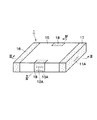
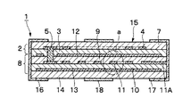
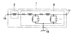
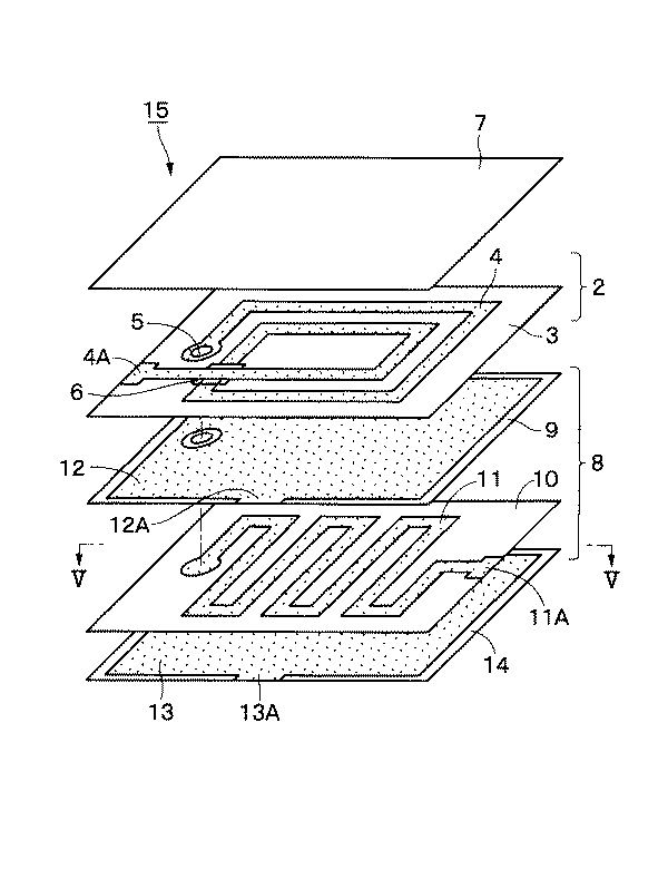
図1ないし図6は第1の実施の形態に係り、1は本実施の形態によるノイズフィルタで、該ノイズフィルタ1は後述するインダクタ部2とフィルタ部8とによって大略構成されている。また、ノイズフィルタ1の遮断周波数fcは、例えば200MHzから2GHz程度の範囲内の値(200MHz≦fc≦2GHz)に設定されている。
【0045】
2はダンピング抵抗をなすインダクタ部で、該インダクタ部2は、インダクタ用磁性体シート3と、該インダクタ用磁性体シート3の表面に設けられたインダクタ用伝送線路4とによって構成されている。ここで、インダクタ用磁性体シート3は、略四角形の板状に形成され、例えばフェライト等の磁性特性を有するセラミックス材料によって形成されている。
【0046】
また、インダクタ用伝送線路4は、例えば銀ペースト、パラジウム等の導電性金属材料によって渦巻き状に形成され、その一端側がインダクタ用磁性体シート3の長さ方向(図1中の左,右方向)一端側に向けて延びると共に、後述の信号用外部電極16に接続された電極部4Aをなしている。一方、インダクタ用伝送線路4の他端側は、磁性体シート3,9を貫通して内部に導電性ペースト等が充填されたスルーホール5を通じて後述のフィルタ用伝送線路11に接続されている。
【0047】
そして、インダクタ用伝送線路4の特性インピーダンス値は、例えば高周波信号のクロック周波数においてノイズフィルタ1の接続対象となる後述の伝送線路22の特性インピーダンス値とドライバIC21の出力インピーダンス値との差の値と同程度の値に設定されている。
【0048】
なお、インダクタ用伝送線路4のうち自身を跨ぐ途中部位はフェライト等からなる絶縁膜6によって覆われている。これにより、インダクタ用伝送線路4の途中部位が短絡するのを防いでいる。また、インダクタ用磁性体シート3の表面には、インダクタ用伝送線路4を覆う保護膜としての磁性体シート7が設けられている。
【0049】
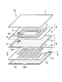
8は分布定数型フィルタをなすフィルタ部で、該フィルタ部8は、インダクタ用磁性体シート3の裏面側に積み重ねて設けられた2枚のフィルタ用磁性体シート9,10と、該磁性体シート9,10の間に設けられインダクタ用伝送線路4に直列接続された後述のフィルタ用伝送線路11と、伝送線路11を含んで磁性体シート9,10を挟む後述の2枚のグランド電極12,13によって構成されている。そして、磁性体シート10の裏面側には、グランド電極13を覆う保護膜としての磁性体シート14が設けられている。
【0050】
また、フィルタ用磁性体シート9,10は、インダクタ用磁性体シート3とほぼ同形状をなす略四角形の板状に形成され、例えばフェライト等の磁性特性を有するセラミックス材料によって形成されている。そして、2枚のグランド電極12,13に挟まれた磁性体シート9,10は、その比透磁率μrが例えば4から30程度の範囲内の値(4≦μr≦30)に設定されている。
【0051】
また、フィルタ用磁性体シート9,10は、磁性体シート3,7,14と相互に重なり合って積層した状態でプレスした後に焼成される。これにより、これらの磁性体シート3,7,9,10,14は積層体15を形成している。
【0052】
なお、磁性体シート9,10と磁性体シート3,7,14とは異なる材料を用いる構成としてもよい。即ち、磁性体シート3にはインダクタ部のインダクタンス値を高めるために磁性体シート9,10よりも比透磁率が大きな材料を用い、磁性体シート7には絶縁性の樹脂皮膜を用い、磁性体シート14にはアルミナ等の絶縁性のセラミック基板(絶縁性基板)を用いてもよい。但し、製造コストの低減するためには、5枚の磁性体シート3,7,9,10,14は全て同じ材料を用いることが好ましい。
【0053】
11はフィルタ用磁性体シート9,10間に配設されたフィルタ用伝送線路で、該フィルタ用伝送線路11は、例えば銀ペースト、パラジウム等の導電性金属材料によってジグザグ状に蛇行した略帯状に形成され、その全長に亘って一定の幅寸法Aを有している。そして、フィルタ用伝送線路11の一端側は、磁性体シート3,9を貫通したスルーホール5を通じてインダクタ用伝送線路4に接続されている。一方、フィルタ用伝送線路11の他端側は、磁性体シート9,10の長さ方向他端側に向けて延びると共に、後述の信号用外部電極17に接続された電極部11Aをなしている。そして、フィルタ用伝送線路11は、磁性体シート9,10の厚さ方向に対して2枚のグランド電極12,13間の略中央に位置し、略全長に亘って2枚のグランド電極12,13によって覆われている。
【0054】
ここで、フィルタ用伝送線路11の幅寸法をA、2枚のグランド電極12,13間の距離寸法をB、磁性体シート9,10の透磁率をμ、磁性体シート9,10の誘電率をεとしたときには、伝送線路11の特性インピーダンスWは以下の数2の式に示す値となる。
【0055】
【数2】
また、伝送線路11の長さ寸法L(全長)は、磁性体シート9,10の比透磁率μrに対して例えば以下の数3の式を満たす値に設定されている。
【0057】
【数3】
なお、小型のチップ部品によってノイズフィルタ1を構成する場合には、伝送線路の長さ寸法Lは、例えば100mm以下である必要がある。一方、磁性体シート9,10の比透磁率μrは4≦μr≦30に設定されている。このため、L/√(μr−1)の値は、以下の数4の式に示すように3mm以上かつ20mm以下であることが好ましい。
【0059】
【数4】
12,13は磁性体シート9の表面と磁性体シート10の裏面とにそれぞれ設けられた2枚のグランド電極で、これらのグランド電極12,13は、フィルタ用磁性体シート9,10を上,下方向(厚さ方向)から挟むものである。また、各グランド電極12,13は、例えば銀ペースト、パラジウム等の導電性金属材料を用いて略四角形の平板状に形成され、磁性体シート9,10を略全面に亘って覆っている。さらに、グランド電極12,13のうち略四角状をなす磁性体シート9,10の長さ方向(図2中の左,右方向)中間位置には、幅方向(図2中の前,後方向)両端側に向けて舌状に突出して延びる電極部12A,13Aがそれぞれ設けられ、該電極部12A,13Aは後述のグランド用外部電極18に接続されている。
【0061】
そして、グランド電極12は、フィルタ用磁性体シート9とインダクタ用磁性体シート3との間に挟まれた状態でフィルタ用磁性体シート9の表面に配設されている。一方、グランド電極13は、フィルタ用磁性体シート10の裏面に配設されると共に、保護膜としての磁性体シート14によって覆われている。
【0062】
16,17は積層体15(磁性体シート3,7,9,10,14)の長さ方向両端側にそれぞれ設けられた第1,第2の信号用外部電極で、該各信号用外部電極16,17は、積層体15の端面を覆うと共に、その表面、裏面および側面をも筒状に覆っている。また、信号用外部電極16,17は、例えば積層体15の両端側に導電性金属材料を塗布した後に、この導電性金属材料を焼き付けることによって固定されている。そして、信号用外部電極16はインダクタ用伝送線路4の電極部4Aに接続され、信号用外部電極17はフィルタ用伝送線路11の電極部11Aに接続されている。
【0063】
18は積層体15の長さ方向中間位置で幅方向の両端側にそれぞれ設けられたグランド用外部電極で、該グランド用外部電極18は、略コ字状をなし、積層体15の側面に厚さ方向に沿って帯状に延びると共に、その一部が積層体15の表面と裏面とに延伸している。そして、グランド用外部電極18は、例えば積層体15の側面側に導電性金属材料を塗布した状態で焼き付けることによって固定され、グランド電極12,13の電極部12A,13Aにそれぞれ接続されている。
【0064】
本実施の形態によるノイズフィルタ1は上述の如く構成されるものであり、次にその作動について図1ないし図8を参照しつつ説明する。
【0065】
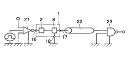
まず、図7に示すように、例えばドライバIC21と伝送線路22を通じてレシーバIC23が接続された回路に対して、ドライバIC21と伝送線路22との間にノイズフィルタ1を接続する。このとき、インダクタ部2に接続された信号用外部電極16をドライバIC21側に接続し、フィルタ部8に接続された信号用外部電極17を伝送線路22側に接続すると共に、グランド用外部電極18をグランド端子に接続する。これにより、ドライバIC21から出力された信号は、インダクタ部2のインダクタ用伝送線路4およびフィルタ部8のフィルタ用伝送線路11を通じて伝送線路22に伝達されると共に、グランド電極12,13はグランド電位に保持される。
【0066】
ここで、インダクタ用伝送線路4のインダクタンスによってインダクタ部2のインピーダンスが生じるから、インダクタ部2をダンピング抵抗として機能させることができ、ドライバIC21の出力抵抗が低いときでもフィルタ部8に向けて確実に信号を伝達することができる。
【0067】
また、フィルタ部8は図8に示すように分布定数型のフィルタを構成すると共に、磁性体シート9,10を構成するフェライト等の磁性材料はフィルタ用伝送線路11を通過する信号の周波数が高くなるに従って信号の熱損失が増大する傾向がある。このため、このような熱損失を用いることによって低域通過型フィルタを構成することができるから、伝送線路11は、例えば200MHzから2GHz程度に設定された遮断周波数fcよりも低い周波数(100MHz〜1GHz程度)の信号を通過させ、これよりも高い周波数の信号をノイズとして減衰し、抑制することができる。
【0068】
また、伝送線路11の幅寸法A、磁性体シート9,10の厚さ寸法(グランド電極12,13間の距離寸法B)を適宜設定することによってフィルタ部8の特性インピーダンスWを設定することができる。さらに、磁性材料の比誘電率は信号の周波数に関係なくほぼ一定値となるから、特性インピーダンスWを信号の周波数に依らずほぼ一定値に保持することができる。このため、ノイズフィルタ1に接続される回路に対して、ほぼ全ての周波数領域についてインピーダンス整合を取ることができ、ノイズフィルタ1の反射損失を低下させ、共振によるノイズの増大を防止することができる。
【0069】
さらに、2枚の磁性体シート9,10間に伝送線路11を配設すると共に、当該2枚の磁性体シート9,10を2枚のグランド電極12,13によって挟む構成としたから、2枚のグランド電極12,13によって磁性体シート9,10間に位置する伝送線路11をその全長に亘って覆うことができる。このため、伝送線路11の全長に亘って特性インピーダンスWを一定値に設定できるから、伝送線路11の途中でノイズに反射が生じることがなく、ノイズの共振を抑制することができる。また、伝送線路11を通過する信号をグランド電極12,13間に閉じ込めることができ、通過帯域での信号の減衰を防止できると共に、外部からの伝送線路11中にノイズが混入するのを防ぐことができ、信号を確実に伝達することができる。
【0070】
なお、ノイズフィルタ1の遮断周波数fcは、磁性体シート9,10の磁性材料の組成(磁性体シート9,10の比透磁率μr)および伝送線路11の長さ寸法Lを調整することによって適宜設定できるものである。
【0071】
そこで、次に磁性体シート9,10の比透磁率μrおよび伝送線路11の長さ寸法Lに対する遮断周波数fcの関係について、図9ないし図14を参照しつつ検討する。
【0072】
まず、磁性体シート9,10の比透磁率μrを一定の値として例えば10とし(μr=10)、伝送線路11の長さ寸法Lを5mm、10mm、20mm、50mmにそれぞれ設定し、フィルタ部8のシミュレーションを行った。この結果、図9に示すように4種類の伝送線路11の長さ寸法Lに対応して、4本の減衰曲線を得た。
【0073】
図9の結果より、伝送線路11の長さ寸法Lが長くなるに従って、遮断周波数fc(減衰量が−3dBとなる周波数)は低下すると共に、例えば減衰量が−10dB付近での減衰曲線の傾き(周波数変化に対する減衰量変化の割合)は増加することが分かる。
【0074】
一方、伝送線路11の長さ寸法Lを一定の値として例えば50mmとし(L=50mm)、磁性体シート9,10の比透磁率μrを3,5,10,20,30にそれぞれ設定し、フィルタ部8のシミュレーションを行った。この結果、図10に示すように5種類の比透磁率μrに対応して、5本の減衰曲線を得た。
【0075】
図10の結果より、比透磁率μrが大きくなるに従って、遮断周波数fcは低下するものの、例えば減衰量が−10dB付近での減衰曲線の傾きは減少することが分かる。
【0076】
これらの特性を本願発明者等が鋭意検討した結果、伝送線路11の長さ寸法Lと磁性体シート9,10の比透磁率μrとに基づいて以下の数5の式によって定まる定数C[mm]が同一となる場合に、長さ寸法L、比透磁率μrが異なるときであっても、減衰曲線の形状(傾き)はほぼ同一となることが分かった。
【0077】
【数5】
例えば、図11は、定数Cを一定の値として例えば20mmとし(C=20mm)、磁性体シート9,10の比透磁率μrを3,5,10,20,30にそれぞれ設定すると共に、伝送線路11の長さ寸法Lを35mm、45mm、63mm、89mm、109mmにそれぞれ設定し、シミュレーションを行った場合の減衰曲線を示している。
【0079】
また、図12は、定数Cを一定の値として例えば3mmとし(C=3mm)、磁性体シート9,10の比透磁率μrを3,5,10,20,30にそれぞれ設定すると共に、伝送線路11の長さ寸法Lを5.19mm、6.72mm、9.48mm、13.4mm、16.4mmにそれぞれ設定し、シミュレーションを行った場合の減衰曲線を示している。
【0080】
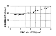
このように、定数Cが同一となる場合には、比透磁率μrが大きくなるに従って、遮断周波数fcは低下するものの、長さ寸法L、比透磁率μrが異なるときでも、減衰曲線の形状(傾き)はほぼ同一となる。また、定数Cは大きくなるに従って、減衰曲線の傾きは大きくなる。
【0081】
そこで、定数Cと減衰量が−10dB付近での減衰曲線の傾きとの関係を検討したところ、図11に示す結果を得た。ここで、一般にノイズ対策に用いられるバイパスコンデンサの減衰曲線の傾きは20dB/dec.であり、ノイズ対策部品として用いるにはこれ以上の傾きを有していることが望ましい。図11の結果より、定数Cが3mm以上であれば、減衰曲線の傾きが20dB/dec.以上となり、ノイズ対策部品として優れた効果を発揮することが分かる。
【0082】
また、図11および図12の結果より、比透磁率μrが同じ値となる場合には、定数Cが小さくなるに従って、遮断周波数fc(減衰量が−3dBとなる周波数)が高くなることが分かる。このため、フィルタ部8の最高の遮断周波数fcを検討するために、定数Cを3mmとし(C=3mm)、比透磁率μrと遮断周波数fcとの関係を検討した。この結果を図14に示す。
【0083】
ここで、近年は、デジタル機器同士で情報伝達を行う手段として無線LANが普及し始めており、この無線LANには例えば2.45GHzおよび5GHz程度の高周波の信号が用いられている。このため、これらの高周波の信号に対してデジタル機器内の低周波(数百MHz程度)の信号を保護するためには、遮断周波数が2GHz以下であるノイズフィルタが必要となっている。そこで、図14の結果を検討すると、遮断周波数fcを2GHzに設定するためには、比透磁率μrを4程度に設定すればよいことが分かる。
【0084】
なお、数5の式によれば、定数Cは√(μr−1)に反比例しているから、伝送線路11の長さ寸法Lが一定であれば、比透磁率μrは小さい値に設定した方が、定数Cを大きくして減衰曲線の傾きを大きくすることができる。また、定数Cが一定であれば、比透磁率μrは小さい値に設定した方が、伝送線路11の長さ寸法Lを短くすることができ、ノイズフィルタ1を小型化することができる。
【0085】
従って、比透磁率μrはできるだけ小さい値として4程度に設定することが望ましい。但し、図14の結果によれば、定数Cが最小値である3mmとしたとき(C=3mm)に、比透磁率μrは30程度に設定しても、遮断周波数fcをデジタル機器等で必要となる200MHz程度に設定することができる。このため、比透磁率μrは、4以上かつ30以下の範囲内(4≦μr≦30)に設定することが好ましい。
【0086】
また、伝送線路11の長さ寸法Lは、長くなるほど定数Cが増大するから、できるだけ長い値に設定することが好ましい。しかし、長さ寸法Lが長くなるに従ってノイズフィルタ1の全体形状が大きくなるから、ノイズフィルタ1を実用的な大きさにするためには、長さ寸法Lはおよそ100mm以下である必要がある。ここで、比透磁率μrの最小値は4だから、定数Cの最大値はおよそ20程度となる。従って、定数Cは、3mm以上かつ20mm以下の範囲内(3mm≦C≦20mm)に設定することが好ましい。
【0087】
かくして、本実施の形態によれば、ノイズフィルタ1にはインダクタ用磁性体シート3とインダクタ用伝送線路4とからなるインダクタ部2を設けたから、伝送線路4のインピーダンスによってインダクタ部2をダンピング抵抗として機能させることができ、ドライバIC21の出力抵抗が低いときでもフィルタ部8に向けて確実に信号を伝達することができる。
【0088】
また、インダクタ部2とフィルタ部8とを一体形成してノイズフィルタ1を構成したから、ダンピング抵抗を別途接続する必要がなく、ダンピング抵抗の組み付けに伴う手間を省くことができる。さらに、インダクタ部2はフィルタ部8と同様に磁性体シート3と伝送線路4とによって構成したから、フィルタ部8と同様の製造工程を付加することによって、容易にインダクタ部2を形成することができる。このため、ダンピング抵抗とノイズフィルタとを別途製造した場合に比べて、製造コストを低減することができる。
【0089】
また、インダクタ用伝送線路4のインピーダンス値は、信号周波数において接続対象となる伝送線路22の特性インピーダンス値とドライバIC21の出力インピーダンス値との差の値と同程度の値に設定したから、これらの伝送線路4,22間でインピーダンス整合を取ることができ、高周波信号の反射を小さくすることができる。
【0090】
さらに、インダクタ部2の伝送線路4を渦巻き状に形成したから、伝送線路4によって形成される磁束を相互に足し合わせてインダクタンスを大きくすることができ、インダクタ部2のインピーダンスを高めることができる。
【0091】
また、フィルタ部8では2枚のフィルタ用磁性体シート9,10間にフィルタ用伝送線路11と配設すると共に、これらの磁性体シート9,10を2枚のグランド電極12,13によって覆う構成としたから、磁性体シート9,10を構成する磁性材料の熱損失を用いることによってノイズを抑制することができる。また、伝送線路11の特性インピーダンスWを信号の周波数に依らずほぼ一定値に保持することができるから、外部の回路とのインピーダンス整合を容易に取ることができる。このため、ノイズフィルタ1の反射損失を低下させることができ、共振によるノイズの増大を防止することができる。
【0092】
また、フィルタ部8の2枚のグランド電極12,13によって磁性体シート9,10間に位置する伝送線路11をその全長に亘って覆うことができるから、伝送線路11の全長に亘って特性インピーダンスWを一定値に設定することができ、伝送線路11の途中でノイズが反射することがないのに加え、伝送線路11を通過する信号をグランド電極12,13間に閉じ込めることができる。このため、通過帯域での信号の減衰を防止できると共に、外部からの伝送線路11中にノイズが混入するのを防ぐことができ、信号を確実に伝達することができる。
【0093】
さらに、磁性体シート3,9,10等は略四角状に形成し、該磁性体シート3,9,10の長さ方向両端側には伝送線路4,11にそれぞれ接続された信号用外部電極16,17を設け、該磁性体シート3,9,10の長さ方向中間位置にはグランド電極12,13に接続されたグランド用外部電極18を設ける構成としたから、直線状に延びる配線の途中に磁性体シート3,9,10の長さ方向両端側に位置する信号用外部電極16,17を容易に接続することができる。また、磁性体シート3,9,10の長さ方向中間位置に設けられたグランド用外部電極18も配線の周辺に設けられたグランド端子に容易に接続することができるから、ノイズフィルタ1の組付け性を向上することができる。
【0094】
また、磁性体シート9,10の比透磁率μrを4≦μr≦30の範囲内に設定すると共に、定数Cが3mm以上(C≧3mm)となるように、伝送線路11の長さ寸法Lを設定したから、遮断周波数fcの範囲を容易に実用的な周波数帯である200MHz≦fc≦2GHzの範囲内に設定することができる。さらに、ノイズの減衰曲線の傾きは、伝送線路11の長さ寸法Lに比例して大きくなると共に、√(μr−1)に反比例して大きくなる傾向がある。このため、磁性体シート9,10の比透磁率μrを4≦μr≦30の範囲に設定し、定数Cを3mm以上に設定することによって、ノイズの減衰曲線の傾きを例えば20dB/dec.以上にすることができる。この結果、信号とノイズとの減衰量の差を大きくすることができるから、信号は減衰させずに通過させることができると共に、ノイズを確実に減衰させることができる。
【0095】
さらに、フィルタ用伝送線路11は蛇行したジグザグ状に形成したから、伝送線路11を直線状に形成した場合に比べて、その長さ寸法Lを増加させることができ、ノイズの減衰量を増加させることができる。
【0096】
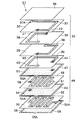
次に、図15ないし図18は本発明の第2の実施の形態によるノイズフィルタを示し、本実施の形態によるノイズフィルタの特徴は、インダクタ部を複数枚のインダクタ用磁性体シート間に設けられた複数層のインダクタ用伝送線路を直列接続することによって構成し、フィルタ部を複数枚のフィルタ用磁性体シート間にフィルタ用伝送線路とグランド電極とを交互に積み重ね、複数層のフィルタ用伝送線路を直列接続する構成としたことにある。
【0097】
31は本実施の形態によるノイズフィルタで、該ノイズフィルタ31は後述するインダクタ部32とフィルタ部46とによって大略構成されている。
【0098】
32はダンピング抵抗をなすインダクタ部で、該インダクタ部32は、例えば4枚のインダクタ用磁性体シート33〜36と、該インダクタ用磁性体シート33〜36の表面にそれぞれ設けられた後述のインダクタ用伝送線路37〜40とによって構成されている。そして、インダクタ用磁性体シート33〜36は、略四角形の板状に形成され、例えばフェライト等の磁性特性を有するセラミックス材料によって形成されている。
【0099】
37〜40は磁性体シート33〜36の表面にそれぞれ配設された合計4層のインダクタ用伝送線路で、該各伝送線路37〜40は、導電性金属材料によって折返し部を有する略コ字状または円弧状をなして形成されている。
【0100】
ここで、伝送線路37の一端側は、インダクタ用磁性体シート33の一端側に向けて延びると共に、後述の信号用外部電極59に接続された電極部37Aをなしている。一方、伝送線路37の他端側は、磁性体シート33を貫通して内部に導電性ペースト等が充填されたスルーホール41を通じて伝送線路38の一端側に接続されている。また、伝送線路38の他端側は磁性体シート34を貫通するスルーホール42を通じて伝送線路39の一端側に接続され、伝送線路39の他端側は磁性体シート35を貫通するスルーホール43を通じて伝送線路40の一端側に接続されている。さらに、伝送線路40の他端側は磁性体シート36,47を貫通するスルーホール44を通じて後述のフィルタ用伝送線路51の一端側に接続されている。
【0101】
これにより、伝送線路37〜40は、互いに直列接続され、磁性体シート33〜36の厚さ方向に対して略四角形または円形の開口を有する枠型のコイル状(螺旋状)をなしている。
【0102】
また、インダクタ用伝送線路37〜40のインピーダンス値は、例えば高周波信号のクロック周波数においてノイズフィルタ1の接続対象となる伝送線路の特性インピーダンス値とドライバICの出力インピーダンス値との差の値と同程度の値に設定されている。さらに、インダクタ用磁性体シート33の表面には、インダクタ用伝送線路37を覆う保護膜としての磁性体シート45が設けられている。
【0103】
46は分布定数型フィルタをなすフィルタ部で、該フィルタ部46は、最裏面側のインダクタ用磁性体シート36に対してその裏面に積み重ねて設けられた4枚のフィルタ用磁性体シート47〜50と、磁性体シート47,48間と磁性体シート49,50間にそれぞれ設けられ互いに直列接続された後述のフィルタ用伝送線路51,52と、磁性体シート47の表面、磁性体シート48,49間、磁性体シート50の裏面にそれぞれ設けられた後述する3枚のグランド電極53〜55によって構成されている。
【0104】
これにより、最表面層と最裏面層とにグランド電極53,55が配置される状態で磁性体シート47〜50間には伝送線路51,52とグランド電極54とが交互に積み重ねられている。また、磁性体シート50の裏面側には、グランド電極55を覆う保護膜としての磁性体シート56が設けられている。
【0105】
そして、フィルタ用磁性体シート47〜50は、グランド電極53〜55に挟まれると共に、インダクタ用磁性体シート33〜36とほぼ同形状の略四角形の板状をなし、第1の実施の形態による磁性体シート9,10とほぼ同様のフェライト等の磁性特性を有するセラミックス材料によって形成されている。
【0106】
また、フィルタ用磁性体シート47〜50は、磁性体シート33〜36,45,56と相互に重なり合って積層した状態でプレスした後に焼成される。これにより、これらの磁性体シート33〜36,45,47〜50,56は積層体57を形成している。
【0107】
51,52はフィルタ用磁性体シート47,48間とフィルタ用磁性体シート49,50間にそれぞれ配設されたフィルタ用伝送線路で、該フィルタ用伝送線路51は、第1の実施の形態による伝送線路11とほぼ同様に例えば銀ペースト、パラジウム等の導電性金属材料によってジグザグ状に蛇行した略帯状に形成され、その全長に亘って一定の幅寸法を有している。
【0108】
そして、フィルタ用伝送線路51の一端側は、磁性体シート36,47を貫通したスルーホール44を通じてインダクタ用伝送線路40に接続され、フィルタ用伝送線路51の他端側は、磁性体シート48,49を貫通したスルーホール58を通じてフィルタ用伝送線路52の一端側に接続されている。また、フィルタ用伝送線路52の他端側は、磁性体シート50の長さ方向他端側に向けて延びると共に、後述の信号用外部電極60に接続された電極部52Aをなしている。
【0109】
そして、伝送線路51,52の特性インピーダンスは、第1の実施の形態による伝送線路11と同様に伝送線路51,52の幅寸法、隣り合うグランド電極53〜55間の距離寸法、磁性体シート47〜50の透磁率、誘電率によって決定される。このため、伝送線路51,52の幅寸法をほぼ等しい値に設定すると共に、磁性体シート47〜50の厚さ寸法をほぼ等しい値に設定することによって、伝送線路51,52の全長に亘って特性インピーダンスを一定値に設定することができる。
【0110】
53〜55は各層の伝送線路51,52を挟むように磁性体シート47〜50の間にそれぞれ設けられた合計3枚のグランド電極で、グランド電極53は磁性体シート47の表面に配置され、グランド電極54は磁性体シート48,49の間に配置されると共に、グランド電極55は磁性体シート50の裏面に配置されている。
【0111】
そして、グランド電極53〜55は、導電性金属材料を用いて略四角形の平板状に形成され、磁性体シート47〜50を略全面に亘って覆っている。さらに、グランド電極53〜55には第1の実施の形態によるグランド電極12,13とほぼ同様に幅方向両端側に向けて突出した電極部53A〜55Aが設けられ、該電極部53A〜55Aは後述のグランド用外部電極61に接続されている。
【0112】
59,60は積層体57(磁性体シート33〜36,45,47〜50,56)の長さ方向両端側にそれぞれ設けられた導電性金属材料からなる第1,第2の信号用外部電極で、該各信号用外部電極59,60は、第1の実施の形態による信号用外部電極16,17と同様に積層体57の端面を覆うと共に、その表面、裏面および側面をも筒状に覆っている。そして、信号用外部電極59はインダクタ用伝送線路37の電極部37Aに接続され、信号用外部電極60はフィルタ用伝送線路52の電極部52Aに接続されている。
【0113】
61は積層体57の長さ方向中間位置で幅方向の両端側にそれぞれ設けられた導電性金属材料からなるグランド用外部電極で、該グランド用外部電極61は、略コ字形状をなし、積層体57の側面に厚さ方向に沿って帯状に延びると共に、その一部が積層体57の表面と裏面とに延伸している。そして、グランド用外部電極61は、グランド電極53〜55の電極部53A〜55Aに接続されている。
【0114】
かくして、このように構成される本実施の形態でも、前記第1の実施の形態とほぼ同様の作用効果を得ることができるが、特に本実施の形態では、インダクタ部32を複数層の伝送線路37〜40を直列接続することによって構成すると共に、フィルタ部46を複数層の伝送線路51,52を直列接続することによって構成している。このため、インダクタ部32、フィルタ部46のインピーダンスを高めることができると共に、フィルタ部46を通過するノイズに対する熱損失を増大させ、その減衰量を増加させることができる。
【0115】
また、伝送線路51,52の幅寸法、磁性体シート47〜50の厚さ寸法を全てほぼ等しい値に設定することによって、積層された各層の伝送線路51,52での特性インピーダンスを相互にほぼ一致させることができるから、伝送線路51,52の途中で特性インピーダンスが変化することがなく、外部の回路との間でインピーダンス整合を容易に取ることができる。
【0116】
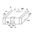
次に、図19は本発明の第3の実施の形態によるノイズフィルタを示し、本実施の形態によるノイズフィルタの特徴は、インダクタ用磁性体シートの裏面にフィルタ用磁性体シートを設け、該フィルタ用磁性体シートの裏面にフィルタ用伝送線路と設けると共に、インダクタ用磁性体シートとフィルタ用磁性体シートとの間にグランド電極を設けることによってフィルタ部を構成したことにある。なお、本実施の形態では第1の実施の形態と同一の構成要素に同一の符合を付し、その説明を省略するものとする。
【0117】
71は本実施の形態によるフィルタ部で、該フィルタ部71は、インダクタ用磁性体シート3の裏面側に積み重ねて設けられた1枚のフィルタ用磁性体シート72と、該磁性体シート72の裏面に設けられインダクタ用伝送線路4に直列接続された後述のフィルタ用伝送線路73と、磁性体シート3,72の間に位置して磁性体シート72の表面に設けられた後述のグランド電極74とによって構成されている。そして、磁性体シート72の裏面側には、グランド電極74を覆う保護膜としての磁性体シート75が設けられている。
【0118】
また、フィルタ用磁性体シート72は、インダクタ用磁性体シート3とほぼ同形状をなす略四角形の板状に形成され、例えばフェライト等の磁性特性を有するセラミックス材料によって形成されている。そして、フィルタ用磁性体シート72は、磁性体シート3,7,75と相互に重なり合って積層した状態でプレスした後に焼成される。これにより、これらの磁性体シート3,7,72,75は積層体76を形成している。
【0119】
73はフィルタ用磁性体シート72の裏面に配設されたフィルタ用伝送線路で、該フィルタ用伝送線路73は、第1の実施の形態による伝送線路11とほぼ同様に導電性金属材料によってジグザグ状に蛇行した略帯状に形成され、その全長に亘って一定の幅寸法を有している。そして、フィルタ用伝送線路73の一端側は、磁性体シート3,72を貫通したスルーホール5を通じてインダクタ用伝送線路4に接続されている。一方、フィルタ用伝送線路73の他端側は、磁性体シート72の長さ方向他端側に向けて延びると共に、第2の信号用外部電極(図示せず)に接続された電極部73Aをなしている。
【0120】
74は磁性体シート3,72間に位置して磁性体シート72の表面に設けられたグランド電極で、該グランド電極74は、第1の実施の形態によるグランド電極12等とほぼ同様に導電性金属材料を用いて略四角形の平板状に形成され、磁性体シート72を略全面に亘って覆っている。また、グランド電極74には電極部74Aが設けられ、該電極部74Aはグランド用外部電極(図示せず)に接続されている。
【0121】
かくして、本実施の形態では、磁性体シート72の裏面に伝送線路73を設けると共に、磁性体シート72の表面に設けたグランド電極74によって該伝送線路73を覆うことによってフィルタ部71を構成したから、第1の実施の形態と同様に、磁性体シート72等の熱損失を利用してノイズを抑制することができる。
【0122】
また、伝送線路73の幅寸法、磁性体シート72の厚さ寸法を適宜設定することによって、ノイズフィルタの特性インピーダンスを設定することができると共に、該特性インピーダンスを信号の周波数に依らずほぼ一定値に保持することができる。このため、ほぼ全ての周波数領域についてノイズフィルタに接続される回路に対するインピーダンス整合を取ることができ、ノイズフィルタの反射損失を低下させることができる。
【0123】
さらに、グランド電極74によって伝送線路73を全長に亘って覆うから、伝送線路73の全長に亘って特性インピーダンスを一定値に設定でき、伝送線路73の途中でノイズが反射するのを防止でき、ノイズの共振を抑制することができる。
【0124】
特に、本実施の形態では、1枚のグランド電極74を用いてフィルタ部71を構成するから、2枚のグランド電極を用いる場合に比べてフィルタ部71の構成を簡略化することができ、製造コストを低減することができる。
【0125】
なお、前記第1,第3の実施の形態では、1枚の磁性体シート3と1層の伝送線路4とからなるインダクタ部2をフィルタ部8,71に接続する構成とした。しかし、本発明はこれに限らず、例えば第2の実施の形態のように複数枚の磁性体シート33〜36と複数層の伝送線路37〜40からなるインダクタ部32を第1,第3の実施の形態によるフィルタ部8,71に接続する構成としてもよい。
【0126】
また、前記第1の実施の形態では、2枚の磁性体シート9,10間に伝送線路11を挟んだ状態でこれらの磁性体シート9,10を2枚のグランド電極12,13で挟むことによってフィルタ部8を構成し、該フィルタ部8をインダクタ部2に接続する構成とした。しかし、本発明はこれに限らず、例えば第2の実施の形態のように複数枚の磁性体シート47〜50間に伝送線路51,52とグランド電極53〜55とを交互の配設したフィルタ部46を第1の実施の形態によるインダクタ部2に接続する構成としてもよい。
【0127】
また、前記各実施の形態では、フィルタ用伝送線路11,51,52,73は蛇行したジグザグ状に形成するものとしたが、直線状や渦巻き状に形成する構成としてもよく、第2の実施の形態のインダクタ部32のように複数層に亘ってコイル状(螺旋状)に形成する構成としてもよい。
【0128】
また、図20に示す第1の変形例のようにフィルタ部8′のグランド電極12′,13′の厚さ寸法T1を伝送線路11′の厚さ寸法T2よりも薄く形成してもよい。これにより、ノイズフィルタ全体の厚さ寸法を薄くすることができ、小型化を図ることができる。また、伝送線路11′の厚さ寸法T2をグランド電極12′,13′の厚さ寸法T1に比べて厚くすることができるから、伝送線路11′の直流抵抗を小さくすることができ、より大きな電流を流すことができる。
【0129】
また、前記各実施の形態では、単一のノイズフィルタ1,31に単一のインダクタ部2,32とフィルタ部8,46,71を設けるものとしたが、例えば図21に示す第2の変形例のように、単一のノイズフィルタ31′にインダクタ部32′とフィルタ部46′を複数個ずつ設ける構成としてもよい。
【0130】
さらに、前記各実施の形態では、磁性体シート3,9,10,33〜36,47〜50,72をフェライト等のセラミックス材料によって形成し、これらを焼成する構成とした。しかし、本発明はこれに限らず、磁性体シートを樹脂材料にカルボニル鉄等の磁性粉を混入して形成してもよい。これにより、磁性体シートを接着剤を用いて接合することによって、ノイズフィルタを形成することができ、焼成等の製造工程を省くことができ、生産性を向上させることができる。なお、この場合、ノイズフィルタの遮断周波数は混入する磁性粉の組成および樹脂材料と磁性粉との割合および伝送線路の長さ寸法によって設定されるものである。
【0131】
【発明の効果】
以上詳述した通り、請求項1の発明によれば、ダンピング抵抗をなすインダクタ部と、該インダクタ部に接続されノイズを除去するフィルタ部とを一体形成する構成としたから、ダンピング抵抗を別途設ける場合に比べて、組付け作業を簡略化できると共に、製造コストを低減することができる。
【0132】
また、フィルタ部は、2枚のフィルタ用磁性体シート間にフィルタ用伝送線路を設けると共に、これらの磁性体シートを2枚のグランド電極によって挟む構成としたから、フィルタ用磁性体シートの熱損失を用いることによってノイズを抑制することができる。また、フィルタ用伝送線路の特性インピーダンスを信号の周波数に依らずほぼ一定値に保持することができるから、外部の回路とのインピーダンス整合を容易に取ることができ、ノイズフィルタの反射損失を低下させ、ノイズの増幅を防止することができる。
【0133】
さらに、フィルタ部は2枚のフィルタ用磁性体シートを2枚のグランド電極によって挟む構成としたから、フィルタ用伝送線路を通過する信号を2枚のグランド電極間に閉じ込めることができ、通過帯域での信号の減衰を防止できると共に、外部からの伝送線路中にノイズが混入するのを防ぐことができ、信号を確実に伝達することができる。
【0134】
請求項2の発明によれば、インダクタ部を複数枚のインダクタ用磁性体シートと複数層のインダクタ用伝送線路とによって構成したから、請求項1の発明による効果に加えて、インダクタ用伝送線路の全長を長くすることができ、インダクタ部のインピーダンスを高めることができる。
【0135】
請求項3の発明によれば、フィルタ部を複数枚のフィルタ用磁性体シートの間にフィルタ用伝送線路とグランド電極とを交互に配置して構成したから、フィルタ用伝送線路の全長を長くして、フィルタ用伝送線路を通過するノイズの減衰量を増加させることができる。
【0136】
この場合、請求項4の発明のように、フィルタ部に接続されるインダクタ部は複数枚のインダクタ用磁性体シートと複数層のインダクタ用伝送線路とによって構成してもよい。
【0137】
請求項5の発明によれば、1枚のフィルタ用磁性体シートを挟んでフィルタ用伝送線路とグランド電極とをそれぞれ設けることによってフィルタ部を構成したから、請求項1の発明による効果に加えて、フィルタ部の構成を簡略化することができ、製造コストを低減することができる。
【0138】
この場合、請求項6の発明のように、フィルタ部に接続されるインダクタ部は複数枚のインダクタ用磁性体シートと複数層のインダクタ用伝送線路とによって構成してもよい。
【0139】
請求項7の発明によれば、インダクタ用伝送線路のインピーダンス値を信号周波数において接続対象となる伝送線路の特性インピーダンス値とドライバICの出力インピーダンス値との差の値と同程度の値に設定したから、接続対象となる伝送線路とインダクタ用伝送線路との間でインピーダンス整合を取ることができ、伝送すべき高周波信号の反射を小さくして確実に伝搬させることができる。
【0140】
請求項8の発明によれば、フィルタ用伝送線路を蛇行したジグザグ状に形成したから、フィルタ用伝送線路を直線状に形成した場合に比べて、その長さ寸法を増加させることができ、ノイズの減衰量を増加させることができる。
【0141】
請求項9の発明によれば、フィルタ用伝送線路は渦巻き状に形成したから、フィルタ用伝送線路によって形成される磁束を相互に足し合わせることができ、インダクタンスを大きくすることができると共に、フィルタ部のインピーダンスを高めることができる。
【0142】
請求項10の発明によれば、インダクタ用磁性体シートおよびフィルタ用磁性体シートは略四角状に形成し、これら磁性体シートの長さ方向両端側にはインダクタ用伝送線路とフィルタ用伝送線路とがそれぞれ接続された第1,第2の信号用外部電極を設け、これら磁性体シートの長さ方向中間位置にはグランド電極に接続されたグランド用外部電極を設ける構成としたから、直線状に延びる配線の途中に磁性体シートの長さ方向両端側に位置する信号用外部電極を容易に接続することができる。また、磁性体シートの長さ方向中間位置に設けられたグランド用外部電極も配線の周辺に設けられたグランド端子に容易に接続することができるから、ノイズフィルタの組付け性を向上することができる。
【0143】
請求項11の発明によれば、フィルタ用磁性体シートの比透磁率μrを4≦μr≦30の範囲内に設定すると共に、L/√(μr−1)≧3となるようにフィルタ用伝送線路の長さ寸法Lを設定したから、遮断周波数の範囲を容易に実用的な周波数帯である200MHz≦fc≦2GHzの範囲内に設定することができる。また、フィルタ用磁性体シートの比透磁率μrを4≦μr≦30の範囲に設定し、L/√(μr−1)≧3に設定したから、ノイズの減衰曲線の傾きを例えば20dB/dec.以上にすることができ、信号とノイズとの減衰量の差を大きくすることができる。
【0144】
請求項12の発明によれば、グランド電極の厚さ寸法をフィルタ用伝送線路の厚さ寸法よりも薄く形成したから、ノイズフィルタ全体の厚さ寸法を薄くすることができ、小型化を図ることができる。また、フィルタ用伝送線路の厚さ寸法をグランド電極に比べて厚くすることができるから、伝送線路の直流抵抗を小さくすることができ、より大きな電流を流すことができる。
【0145】
請求項13の発明によれば、磁性体シートは磁性特性をもったセラミックス材料によって形成したから、磁性体シートを重ね合わせた状態で焼成することによってノイズフィルタを形成することができる。この場合、請求項14の発明のように、磁性体シートを焼結したフェライトによって形成することが好ましい。
【0146】
請求項15の発明によれば、磁性体シートは磁性粉を混入した樹脂材料によって形成したから、磁性体シートを接着剤を用いて接合することによって、ノイズフィルタを形成することができ、焼成等の製造工程を省くことができ、生産性を向上させることができる。
【図面の簡単な説明】
【図1】第1の実施の形態によるノイズフィルタを示す斜視図である。
【図2】図1中のノイズフィルタを分解して示す分解斜視図である。
【図3】ノイズフィルタを図1中の矢示III−III方向からみた断面図である。
【図4】ノイズフィルタを図1中の矢示IV−IV方向からみた断面図である。
【図5】フィルタ用伝送線路等を図2中の矢示V−V方向からみた平面図である。
【図6】図3中のa部を拡大して示す要部拡大断面図である。
【図7】図1中のノイズフィルタを伝送線路等に接続した状態を示す回路図である。
【図8】図1中のノイズフィルタを示す等価回路図である。
【図9】磁性体シートの比透磁率μrを10に設定したときの信号の周波数と減衰量との関係を示す特性線図である。
【図10】フィルタ用伝送線路の長さ寸法Lを50mmに設定したときの信号の周波数と減衰量との関係を示す特性線図である。
【図11】定数Cを20mmに設定したときの信号の周波数と減衰量との関係を示す特性線図である。
【図12】定数Cを3mmに設定したときの信号の周波数と減衰量との関係を示す特性線図である。
【図13】定数Cと減衰曲線の傾きとの関係を示す特性線図である。
【図14】遮断周波数fcとフィルタ用磁性体シートの比透磁率μrとの関係を示す特性線図である。
【図15】第2の実施の形態によるノイズフィルタを示す斜視図である。
【図16】図15中のノイズフィルタを分解して示す分解斜視図である。
【図17】ノイズフィルタを図15中の矢示XVII−XVII方向からみた断面図である。
【図18】ノイズフィルタを図15中の矢示XVIII−XVIII方向からみた断面図である。
【図19】第3の実施の形態によるノイズフィルタを分解して示す分解斜視図である。
【図20】第1の変形例によるノイズフィルタのフィルタ部を拡大して示す図6を同様位置の要部拡大断面図である。
【図21】第2の変形例によるノイズフィルタを分解して示す分解斜視図である。
【符号の説明】
1,31,31′ ノイズフィルタ
2,32,32′ インダクタ部
3,33〜36,33′〜36′ インダクタ用磁性体シート
4,37〜40,37′〜40′ インダクタ用伝送線路
8,46,71,8′,46′ フィルタ部
9,10,47〜50,72,47′〜50′ フィルタ用磁性体シート
11,51,52,73,11′,51′,52′ フィルタ用伝送線路
12,13,53〜55,74,12′,13′,53′〜55′ グランド電極
16,17,59,60 信号用外部電極
18,61 グランド用外部電極[0001]
TECHNICAL FIELD OF THE INVENTION
The present invention relates to a noise filter suitable for suppressing electromagnetic noise interference of an electronic device.
[0002]
[Prior art]
2. Description of the Related Art In general, various types of noise filters are used to suppress electromagnetic noise interference of electronic devices. As a conventional noise filter, there is known a filter formed by a lumped constant circuit such as a three-terminal capacitor (for example, see Patent Document 1). In such a noise filter according to the related art, noise is suppressed by using a reflection loss that increases a reflection coefficient at a frequency that becomes noise (noise).
[0003]
Further, as another conventional noise filter, a noise filter in which a circuit including a large number of inductors, capacitors, and the like is formed is also known (for example, see Patent Document 2).
[0004]
[Patent Document 1]
JP-A-10-154632
[Patent Document 2]
JP 2000-348944 A
[0005]
[Problems to be solved by the invention]
By the way, in the above-described prior art, since noise is suppressed by reflection loss, for example, when a noise filter is provided in a line connecting between circuits, a specific frequency between the noise filter and a peripheral circuit is reduced. There has been a problem that noise may resonate, rather amplifying the noise.
[0006]
In particular, in recent years, the signal frequency used for digital devices tends to be higher, and electronic devices having a signal frequency exceeding 100 MHz are increasing. For this reason, a low-pass filter having a cutoff frequency of 200 MHz or more is required. For example, a high-frequency signal having a line length between a noise filter and surrounding components, a line length between a plurality of components, or the like is 200 MHz or more. Is a length dimension that easily resonates. Therefore, a noise filter using return loss as in the related art tends to be difficult to use for electronic devices having a signal frequency exceeding 100 MHz.
[0007]
Further, in another conventional technique, the resonance phenomenon is suppressed by reducing the reflection loss. However, in other conventional noise filters, since a circuit is formed by connecting a large number of inductors, capacitors, and the like, the structure is complicated, miniaturization is difficult, manufacturing costs are increased, and the noise filter is not chip-shaped. Therefore, there is a problem that it is difficult to attach to a printed wiring.
[0008]
Further, when the output resistance of the driver IC connected to the noise filter is low, a damping resistor is separately connected between the noise filter and the driver IC in order to suppress resonance between the driver IC and peripheral circuits. . In this case, it is necessary to prepare two parts, a noise filter and a damping resistor, and to mount each of these two parts. Therefore, the manufacturing cost is easily increased, and the mounting time is increased, and the productivity is increased. There is also a problem that is reduced.
[0009]
SUMMARY OF THE INVENTION The present invention has been made in view of the above-described problems of the related art, and an object of the present invention is to provide a small and inexpensive noise filter that can prevent noise resonance and has a damping resistor.
[0010]
[Means for Solving the Problems]
In order to solve the above-described problem, the invention according to
[0011]
With this configuration, an impedance is generated in the inductor portion by the inductance of the transmission line for the inductor, so that the inductor portion can function as a damping resistor. Resonance can be suppressed.
[0012]
In addition, since the magnetic material constituting the magnetic sheet for the filter increases the heat loss of the signal as the frequency of the signal passing through the transmission line for the filter increases, noise can be suppressed by using such heat loss. Can be.
[0013]
The characteristic impedance of the filter section can be set by appropriately setting the width of the filter transmission line and the thickness of the magnetic sheet. In particular, since the relative permittivity of the magnetic material has a substantially constant value irrespective of the signal frequency, the characteristic impedance can be maintained at a substantially constant value irrespective of the signal frequency. For this reason, impedance matching can be achieved for circuits connected to the noise filter in almost all frequency ranges, and the reflection loss of the noise filter can be reduced.
[0014]
Further, since the filter transmission line is disposed between the two filter magnetic sheets and the two filter magnetic sheets are sandwiched between the two ground electrodes, the two filter magnetic sheets are sandwiched by the ground electrodes. The filter transmission line located between the body sheets can be covered over its entire length. For this reason, the characteristic impedance can be set to a constant value over the entire length of the filter transmission line, so that no noise is reflected in the middle of the filter transmission line, and noise resonance can be suppressed. Further, a signal passing through the transmission line for the filter can be confined between the two ground electrodes, so that attenuation of the signal in the pass band can be prevented and noise is prevented from being mixed into the transmission line for the filter from the outside. Signal can be transmitted reliably.
[0015]
The invention according to
[0016]
This provides substantially the same function and effect as the first aspect of the present invention, and also connects the inductor transmission lines provided in a plurality of layers in series, so that the impedance of the inductor section can be increased.
[0017]
The invention according to
[0018]
Accordingly, the impedance of the inductor portion functions as a damping resistor, thereby providing a resonance suppressing effect, and transmitting a high-frequency signal to the filter portion reliably. Further, when the high-frequency signal passes through the transmission line for the filter, noise can be suppressed by utilizing the increase in the heat loss of the magnetic sheet for the filter. Furthermore, the characteristic impedance of the filter unit can be set by appropriately setting the width of the filter transmission line and the thickness of the filter magnetic sheet. In particular, since the relative permittivity of the magnetic material is substantially constant regardless of the signal frequency, impedance matching can be achieved between the noise filter and the circuit connected to the noise filter in almost all frequency ranges. Thus, the reflection loss of the noise filter can be reduced.
[0019]
Further, in a state where the ground electrodes are arranged on the outermost surface layer and the outermost back layer of the plurality of overlapping magnetic sheets for filters, the transmission lines for filters and the ground electrodes are alternately stacked between the magnetic sheets for filters. Therefore, the filter transmission line of each layer can be arranged between two filter magnetic sheets, and the filter transmission line of each layer can be covered over the entire length by two ground electrodes. For this reason, a signal passing through the filter transmission line can be confined between the ground electrodes, and signal attenuation in the pass band can be prevented.
[0020]
In addition, since a plurality of overlapping magnetic sheets for a filter have ground electrodes disposed on the outermost surface layer and the outermost surface layer, noise can be prevented from being externally mixed into the transmission line for the filter, and signals can be prevented. It can be transmitted reliably.
[0021]
Further, when the width dimensions of all the filter transmission lines are set to substantially equal values and the thickness dimensions of all the filter magnetic sheets are set to approximately equal values, the characteristics of each layer with respect to the filter transmission lines are set. The impedances can be made to substantially match each other. For this reason, the characteristic impedance can be set to a substantially constant value over the entirety of the filter transmission lines connected in series with each other, so that no noise is reflected in the middle of the filter transmission lines, and the resonance of the noise is suppressed. And impedance matching with an external circuit can be easily achieved.
[0022]
Furthermore, since the filter transmission lines of a plurality of layers are connected in series, the total length of the filter transmission lines can be increased, and the amount of attenuation of noise passing through the filter transmission lines can be increased.
[0023]
The invention according to
[0024]
Thereby, substantially the same operation and effect as the third aspect of the invention can be obtained. Further, since the transmission lines for inductors provided in a plurality of layers are connected in series, the overall length of the transmission line for inductors can be increased, and the characteristic impedance of the inductor section can be increased.
[0025]
The invention according to
[0026]
With this configuration, the impedance of the inductor portion functions as a damping resistor to provide a resonance suppressing effect, and it is possible to reliably transmit a high-frequency signal to the filter portion. The noise of the signal passing through the filter transmission line can be suppressed by utilizing the heat loss. In addition, by appropriately setting the width dimension of the transmission line for the filter and the thickness dimension of the magnetic sheet for the filter, the characteristic impedance of the filter unit can be set, and the characteristic impedance is almost constant regardless of the signal frequency. Can be held to a value. For this reason, impedance matching can be achieved for circuits connected to the noise filter in almost all frequency ranges, and the reflection loss of the noise filter can be reduced. Furthermore, since the filter transmission line is covered over the entire length by the ground electrode, the characteristic impedance can be set to a constant value over the entire length of the filter transmission line, and reflection and resonance of noise can be suppressed.
[0027]
The invention of
[0028]
This makes it possible to obtain substantially the same functions and effects as the invention of
[0029]
In the invention according to
[0030]
Thereby, impedance matching can be achieved between the transmission line to be connected and the transmission line for the inductor, and reflection of a high-frequency signal can be reduced.
[0031]
In the invention of
[0032]
According to the ninth aspect, the transmission line for the filter is formed in a spiral shape. Thus, the magnetic fluxes formed by the filter transmission lines are added together, so that the inductance can be increased and the impedance of the filter section can be increased.
[0033]
According to the tenth aspect of the present invention, the magnetic sheet for the inductor and the magnetic sheet for the filter are formed in a rectangular shape, and the first signal connected to the transmission line for the inductor is provided on one end side in the longitudinal direction of the magnetic sheet. The second external electrode for signal connected to the transmission line for the filter is provided on the other end of the magnetic sheet in the longitudinal direction, and the external electrode for the signal is provided at an intermediate position in the longitudinal direction of the magnetic sheet. An external ground electrode connected to the ground electrode is provided.
[0034]
Thus, the two signal external electrodes located at both ends in the length direction of the magnetic sheet can be easily connected to the middle of the linearly extending wiring. In addition, the ground external electrode provided at the intermediate position in the length direction of the magnetic sheet can be easily connected to the ground terminal provided around the wiring. Therefore, it is possible to improve the assemblability of the noise filter.
[0035]
According to the eleventh aspect of the present invention, the cutoff frequency is in a range of 200 MHz to 2 GHz, and the relative magnetic permeability of the magnetic sheet for a filter is set to μ. r When the length of the filter transmission line is L [mm], 4 ≦ μ r ≦ 30, L / √ (μ r -1) is set to ≧ 3 mm.
[0036]
Here, the relative permeability μ r Is the magnetic permeability μ [H / m] of the magnetic sheet for the filter and the magnetic permeability μ in a vacuum. 0 [H / m] and a value represented by the following equation (1).
[0037]
(Equation 1)
Thus, the relative magnetic permeability μ of the magnetic sheet for filter is r Is 4 ≦ μ r ≦ 30 and L / √ (μ r -1) By setting the length L of the filter transmission line so as to satisfy ≧ 3 mm, the cutoff frequency range can be easily set within the range of 200 MHz ≦ fc ≦ 2 GHz. The slope of the noise attenuation curve (the ratio of the change in the amount of attenuation to the frequency of the signal) increases in proportion to the length L of the transmission line for the filter, and the relative permeability μ of the magnetic sheet for the filter. r √ (μ r -1) tends to increase in inverse proportion. Therefore, the relative magnetic permeability μ of the magnetic sheet for the filter is r Is 4 ≦ μ r ≦ 30, L / √ (μ r -1) By setting ≧ 3 mm, the slope of the noise attenuation curve is set to, for example, 20 dB / dec. As described above, the difference between the signal and noise attenuation can be increased.
[0039]
In a twelfth aspect of the present invention, the thickness of the ground electrode is smaller than the thickness of the transmission line for the filter.
[0040]
Thus, the thickness dimension of the entire noise filter can be reduced, and the size can be reduced. Further, since the thickness of the transmission line can be made larger than that of the ground electrode, the DC resistance of the transmission line can be reduced and a larger current can flow.
[0041]
According to a thirteenth aspect of the present invention, the magnetic sheet for inductor and the magnetic sheet for filter are formed of a ceramic material having magnetic properties. This makes it possible to form a noise filter by firing the magnetic sheets in a stacked state. In this case, it is preferable that each magnetic sheet is formed of sintered ferrite.
[0042]
The invention of
[0043]
BEST MODE FOR CARRYING OUT THE INVENTION
Hereinafter, a noise filter according to an embodiment of the present invention will be described in detail with reference to FIGS.
[0044]
1 to 6 relate to the first embodiment, 1 is a noise filter according to the present embodiment, and the
[0045]
[0046]
Further, the
[0047]
The characteristic impedance value of the
[0048]
A part of the
[0049]
[0050]
The
[0051]
The
[0052]
The
[0053]
[0054]
Here, the width dimension of the
[0055]
(Equation 2)
The length L (overall length) of the
[0057]
[Equation 3]
When the
[0059]
(Equation 4)
[0061]
The
[0062]
[0063]
[0064]
The
[0065]
First, as shown in FIG. 7, a
[0066]
Here, since the inductance of the
[0067]
The
[0068]
The characteristic impedance W of the
[0069]
Further, the
[0070]
The cutoff frequency fc of the
[0071]
Therefore, next, the relative magnetic permeability μ of the
[0072]
First, the relative magnetic permeability μ of the
[0073]
From the results of FIG. 9, as the length L of the
[0074]
On the other hand, the length L of the
[0075]
From the results of FIG. 10, the relative magnetic permeability μ r It can be seen that the cutoff frequency fc decreases as the value increases, but the slope of the attenuation curve decreases, for example, when the attenuation is around -10 dB.
[0076]
As a result of intensive studies of these characteristics by the present inventors, the length L of the
[0077]
(Equation 5)
For example, FIG. 11 shows that the constant C is set to a constant value, for example, 20 mm (C = 20 mm), and the relative magnetic permeability μ r Are set to 3, 5, 10, 20, and 30, respectively, and the length dimension L of the
[0079]
FIG. 12 shows that the constant C is set to a constant value of, for example, 3 mm (C = 3 mm), and the relative magnetic permeability μ of the
[0080]
As described above, when the constant C is the same, the relative permeability μ r Becomes larger, the cutoff frequency fc decreases, but the length L, the relative magnetic permeability μ r Are different, the shape (slope) of the attenuation curve is almost the same. The slope of the attenuation curve increases as the constant C increases.
[0081]
Then, when the relationship between the constant C and the slope of the attenuation curve when the attenuation amount was around -10 dB was examined, the result shown in FIG. 11 was obtained. Here, the slope of the attenuation curve of a bypass capacitor generally used for noise suppression is 20 dB / dec. Therefore, it is desirable to have an inclination greater than this for use as a noise suppression component. According to the results of FIG. 11, when the constant C is 3 mm or more, the slope of the attenuation curve is 20 dB / dec. From the above, it can be seen that excellent effects are exhibited as noise suppression components.
[0082]
Further, from the results of FIGS. 11 and 12, the relative magnetic permeability μ r Have the same value, the cutoff frequency fc (the frequency at which the amount of attenuation is -3 dB) increases as the constant C decreases. For this reason, in order to study the highest cutoff frequency fc of the
[0083]
In recent years, wireless LANs have begun to spread as means for transmitting information between digital devices, and high-frequency signals of, for example, about 2.45 GHz and 5 GHz are used for the wireless LAN. Therefore, in order to protect low-frequency (about several hundred MHz) signals in digital equipment against these high-frequency signals, a noise filter having a cutoff frequency of 2 GHz or less is required. Therefore, considering the results of FIG. 14, it is found that the relative permeability μ r Is set to about 4.
[0084]
According to the equation (5), the constant C is √ (μ r -1), the relative permeability μ is constant if the length L of the
[0085]
Therefore, the relative magnetic permeability μ r Is desirably set to about 4 as a value as small as possible. However, according to the result of FIG. 14, when the constant C is set to the minimum value of 3 mm (C = 3 mm), the relative permeability μ r Even if is set to about 30, the cut-off frequency fc can be set to about 200 MHz required for digital devices and the like. Therefore, the relative permeability μ r Is in the range of 4 or more and 30 or less (4 ≦ μ r ≦ 30).
[0086]
Further, since the constant C increases as the length L of the
[0087]
Thus, according to the present embodiment, since the
[0088]
Further, since the
[0089]
Further, since the impedance value of the
[0090]
Further, since the
[0091]
In the
[0092]
Further, since the
[0093]
Further, the
[0094]
The relative magnetic permeability μ of the
[0095]
Further, since the
[0096]
15 to 18 show a noise filter according to a second embodiment of the present invention. The feature of the noise filter according to the present embodiment is that an inductor portion is provided between a plurality of inductor magnetic sheets. A plurality of layers of the transmission lines for the inductors are connected in series, and the filter section is alternately stacked with the transmission lines for the filters and the ground electrodes between the plurality of magnetic sheets for the filters. Are connected in series.
[0097]
[0098]
[0099]
[0100]
Here, one end of the
[0101]
Thereby, the
[0102]
The impedance value of the
[0103]
[0104]
Thus, the
[0105]
The magnetic sheets for
[0106]
The magnetic sheets for a
[0107]
[0108]
One end of the
[0109]
The characteristic impedances of the
[0110]
[0111]
The
[0112]
[0113]
[0114]
Thus, in the present embodiment configured as described above, substantially the same operation and effect as those in the first embodiment can be obtained. However, in the present embodiment, in particular, in the present embodiment, the
[0115]
By setting the width dimensions of the
[0116]
19 shows a noise filter according to a third embodiment of the present invention. The feature of the noise filter according to the present embodiment is that a magnetic sheet for a filter is provided on the back surface of a magnetic sheet for an inductor. The filter section is configured by providing a transmission line for a filter on the back surface of the magnetic sheet for use and a ground electrode between the magnetic sheet for the inductor and the magnetic sheet for filter. In the present embodiment, the same components as those in the first embodiment are denoted by the same reference numerals, and description thereof will be omitted.
[0117]
[0118]
The magnetic sheet for
[0119]
[0120]
[0121]
Thus, in the present embodiment, since the
[0122]
In addition, by appropriately setting the width dimension of the
[0123]
Further, since the
[0124]
In particular, in the present embodiment, since the
[0125]
In the first and third embodiments, the
[0126]
In the first embodiment, the
[0127]
In the above embodiments, the
[0128]
Further, as in the first modification shown in FIG. 20, the thickness T1 of the ground electrodes 12 'and 13' of the filter section 8 'may be formed smaller than the thickness T2 of the transmission line 11'. Thus, the thickness dimension of the entire noise filter can be reduced, and the size can be reduced. Further, since the thickness T2 of the transmission line 11 'can be made larger than the thickness T1 of the ground electrodes 12' and 13 ', the DC resistance of the transmission line 11' can be reduced, and the transmission line 11 'can be made larger. A current can flow.
[0129]
Further, in each of the above embodiments, the single noise filters 1 and 31 are provided with the
[0130]
Further, in each of the above embodiments, the
[0131]
【The invention's effect】
As described above in detail, according to the first aspect of the present invention, since the inductor portion forming the damping resistor and the filter portion connected to the inductor portion for removing noise are integrally formed, the damping resistor is separately provided. As compared with the case, the assembling work can be simplified and the manufacturing cost can be reduced.
[0132]
In addition, since the filter section has a configuration in which a filter transmission line is provided between two filter magnetic sheets and these magnetic sheets are sandwiched between two ground electrodes, the heat loss of the filter magnetic sheet is reduced. Can suppress noise. Also, since the characteristic impedance of the transmission line for the filter can be maintained at a substantially constant value regardless of the frequency of the signal, impedance matching with an external circuit can be easily achieved, and the reflection loss of the noise filter is reduced. , Noise amplification can be prevented.
[0133]
Further, since the filter section has a configuration in which two magnetic sheets for a filter are sandwiched between two ground electrodes, a signal passing through the transmission line for the filter can be confined between the two ground electrodes, and a pass band can be obtained. Signal can be prevented from attenuating, and noise can be prevented from being mixed into an external transmission line, so that the signal can be transmitted reliably.
[0134]
According to the second aspect of the present invention, since the inductor section is constituted by the plurality of inductor magnetic sheets and the plurality of layers of the transmission lines for the inductor, in addition to the effect of the first aspect of the invention, the transmission section of the inductor is provided. The total length can be increased, and the impedance of the inductor section can be increased.
[0135]
According to the third aspect of the present invention, the filter section is configured by alternately arranging the filter transmission line and the ground electrode between the plurality of filter magnetic sheets, so that the total length of the filter transmission line is increased. Thus, the attenuation of noise passing through the filter transmission line can be increased.
[0136]
In this case, the inductor unit connected to the filter unit may be constituted by a plurality of inductor magnetic sheets and a plurality of inductor transmission lines.
[0137]
According to the fifth aspect of the present invention, the filter section is configured by providing the filter transmission line and the ground electrode with one filter magnetic sheet interposed therebetween. In addition, the configuration of the filter unit can be simplified, and the manufacturing cost can be reduced.
[0138]
In this case, the inductor unit connected to the filter unit may be constituted by a plurality of inductor magnetic sheets and a plurality of inductor transmission lines.
[0139]
According to the seventh aspect of the present invention, the impedance value of the transmission line for the inductor is set to a value substantially equal to the difference between the characteristic impedance value of the transmission line to be connected and the output impedance value of the driver IC at the signal frequency. Therefore, impedance matching can be achieved between the transmission line to be connected and the transmission line for the inductor, and the reflection of the high-frequency signal to be transmitted can be reduced and transmitted reliably.
[0140]
According to the eighth aspect of the present invention, since the filter transmission line is formed in a zigzag shape meandering, the length dimension can be increased as compared with the case where the filter transmission line is formed linearly, and noise can be reduced. Can be increased.
[0141]
According to the ninth aspect of the present invention, since the transmission line for the filter is formed in a spiral shape, the magnetic flux formed by the transmission line for the filter can be added to each other, the inductance can be increased, and the filter unit can be increased. Can be increased.
[0142]
According to the tenth aspect of the present invention, the magnetic sheet for the inductor and the magnetic sheet for the filter are formed in a substantially quadrangular shape. The first and second signal external electrodes are connected to each other, and a ground external electrode connected to the ground electrode is provided at a middle position in the length direction of these magnetic sheets. Signal external electrodes located at both ends in the length direction of the magnetic sheet can be easily connected to the middle of the extending wiring. In addition, the ground external electrode provided at the intermediate position in the length direction of the magnetic sheet can be easily connected to the ground terminal provided around the wiring, so that the noise filter can be easily assembled. it can.
[0143]
According to the eleventh aspect of the present invention, the relative magnetic permeability μ of the magnetic sheet for a filter. r Is 4 ≦ μ r ≦ 30 and L / √ (μ r -1) Since the length L of the filter transmission line is set so as to satisfy ≧ 3, the cutoff frequency range can be easily set within the practical frequency band of 200 MHz ≦ fc ≦ 2 GHz. it can. Also, the relative permeability μ of the magnetic sheet for the filter r Is 4 ≦ μ r ≦ 30, L / √ (μ r -1) ≧ 3, the slope of the noise attenuation curve is set to, for example, 20 dB / dec. As described above, the difference between the signal and noise attenuation can be increased.
[0144]
According to the twelfth aspect of the invention, since the thickness of the ground electrode is formed smaller than the thickness of the transmission line for the filter, the thickness of the entire noise filter can be reduced, and the size can be reduced. Can be. Further, since the thickness of the filter transmission line can be made thicker than the ground electrode, the DC resistance of the transmission line can be reduced, and a larger current can flow.
[0145]
According to the thirteenth aspect of the present invention, since the magnetic material sheet is formed of a ceramic material having magnetic properties, a noise filter can be formed by firing the magnetic material sheets in an overlapping state. In this case, it is preferable that the magnetic material sheet is formed of sintered ferrite.
[0146]
According to the invention of
[Brief description of the drawings]
FIG. 1 is a perspective view showing a noise filter according to a first embodiment.
FIG. 2 is an exploded perspective view showing the noise filter in FIG. 1 in an exploded manner.
FIG. 3 is a cross-sectional view of the noise filter as viewed from a direction indicated by arrows III-III in FIG.
FIG. 4 is a cross-sectional view of the noise filter as viewed from a direction indicated by arrows IV-IV in FIG. 1;
FIG. 5 is a plan view of a transmission line for a filter and the like as viewed from a direction indicated by arrows VV in FIG. 2;
FIG. 6 is an enlarged cross-sectional view showing a main part of FIG.
FIG. 7 is a circuit diagram showing a state in which the noise filter in FIG. 1 is connected to a transmission line or the like.
FIG. 8 is an equivalent circuit diagram showing the noise filter in FIG.
FIG. 9 shows a relative magnetic permeability μ of a magnetic sheet. r FIG. 9 is a characteristic diagram showing a relationship between the frequency of a signal and the amount of attenuation when is set to 10.
FIG. 10 is a characteristic diagram showing the relationship between signal frequency and attenuation when the length L of the filter transmission line is set to 50 mm.
FIG. 11 is a characteristic diagram illustrating a relationship between a signal frequency and an attenuation when a constant C is set to 20 mm.
FIG. 12 is a characteristic diagram showing a relationship between a signal frequency and an attenuation when a constant C is set to 3 mm.
FIG. 13 is a characteristic diagram showing a relationship between a constant C and a slope of an attenuation curve.
FIG. 14 shows a cutoff frequency fc and a relative magnetic permeability μ of a magnetic sheet for a filter. r FIG. 4 is a characteristic diagram showing the relationship between
FIG. 15 is a perspective view showing a noise filter according to a second embodiment.
FIG. 16 is an exploded perspective view showing the noise filter in FIG. 15 in an exploded manner.
17 is a cross-sectional view of the noise filter as viewed from the direction indicated by arrows XVII-XVII in FIG.
FIG. 18 is a cross-sectional view of the noise filter as viewed in a direction indicated by arrows XVIII-XVIII in FIG.
FIG. 19 is an exploded perspective view showing an exploded noise filter according to the third embodiment.
FIG. 20 is an enlarged cross-sectional view of a main part at the same position in FIG. 6 showing an enlarged filter portion of the noise filter according to the first modified example.
FIG. 21 is an exploded perspective view showing a noise filter according to a second modification in an exploded manner.
[Explanation of symbols]
1,31,31 'noise filter
2,32,32 'inductor part
3,33-36,33'-36 'Magnetic sheet for inductor
4,37-40,37'-40 'Transmission line for inductor
8, 46, 71, 8 ', 46' filter section
9,10,47-50,72,47'-50 'Magnetic sheet for filter
11,51,52,73,11 ', 51', 52 'Transmission line for filter
12, 13, 53 to 55, 74, 12 ', 13', 53 'to 55' Ground electrode
16, 17, 59, 60 External electrode for signal
18,61 External electrode for ground
Claims (15)
前記インダクタ部は、インダクタ用磁性体シートと、該インダクタ用磁性体シートの表面に設けられたインダクタ用伝送線路とによって構成し、
前記フィルタ部は、前記インダクタ用磁性体シートの裏面に積み重ねて設けられ互いに重なり合う2枚のフィルタ用磁性体シートと、該2枚の磁性体シート間に配設され前記インダクタ用伝送線路に直列接続されたフィルタ用伝送線路と、前記各フィルタ用磁性体シートに設けられ該フィルタ用伝送線路を含めて前記2枚のフィルタ用磁性体シートを挟む2枚のグランド電極とによって構成してなるノイズフィルタ。A noise filter comprising an inductor part forming a damping resistor and a filter part connected to the inductor part and removing noise,
The inductor portion is configured by a magnetic sheet for inductor and a transmission line for inductor provided on a surface of the magnetic sheet for inductor.
The filter unit is provided on the back surface of the inductor magnetic sheet and is provided with two filter magnetic sheets overlapping each other, and is disposed between the two magnetic sheets and connected in series to the inductor transmission line. Filter comprising: a transmission line for a filter; and two ground electrodes provided on each of the magnetic sheets for the filter, and including the transmission lines for the filter and sandwiching the two magnetic sheets for the filter. .
前記インダクタ部は、互いに重なり合う複数枚のインダクタ用磁性体シートと、該各インダクタ用磁性体シートの表面に設けられ互いに直列接続されたインダクタ用伝送線路とによって構成し、
前記フィルタ部は、前記複数枚のインダクタ用磁性体シートのうち最裏面側のインダクタ用磁性体シートに積み重ねて設けられ互いに重なり合う2枚のフィルタ用磁性体シートと、該2枚の磁性体シート間に配設され前記インダクタ用伝送線路に直列接続されたフィルタ用伝送線路と、前記各フィルタ用磁性体シートに設けられ該フィルタ用伝送線路を含めて前記2枚のフィルタ用磁性体シートを挟む2枚のグランド電極とによって構成してなるノイズフィルタ。A noise filter comprising an inductor part forming a damping resistor and a filter part connected to the inductor part and removing noise,
The inductor unit includes a plurality of inductor magnetic sheets overlapping each other, and an inductor transmission line provided on the surface of each inductor magnetic sheet and connected in series with each other,
The filter section includes two magnetic sheets for a filter, which are stacked on the magnetic sheet for an inductor on the rearmost side of the plurality of magnetic sheets for an inductor and overlap each other, and a space between the two magnetic sheets. And a filter transmission line connected in series to the inductor transmission line, and two filter magnetic sheets provided on each of the filter magnetic sheets and including the filter transmission lines. A noise filter composed of a single ground electrode.
前記インダクタ部は、インダクタ用磁性体シートと、該インダクタ用磁性体シートの表面に設けられたインダクタ用伝送線路とによって構成し、
前記フィルタ部は、前記インダクタ用磁性体シートの裏面に積み重ねて設けられ互いに重なり合う複数枚のフィルタ用磁性体シートと、これら各フィルタ用磁性体シートの最表面層と最裏面層とにグランド電極を配置する状態で、前記各フィルタ用磁性体シート間にフィルタ用伝送線路とグランド電極とを交互に積み重ね、複数層のフィルタ用伝送線路を直列接続すると共に、その一端側を前記インダクタ用伝送線路に直列接続する構成としてなるノイズフィルタ。A noise filter comprising an inductor part forming a damping resistor and a filter part connected to the inductor part and removing noise,
The inductor portion is configured by a magnetic sheet for inductor and a transmission line for inductor provided on a surface of the magnetic sheet for inductor.
The filter section is provided with a plurality of filter magnetic sheets stacked on the back surface of the inductor magnetic sheet and overlapping each other, and ground electrodes on the outermost surface layer and the lowermost layer of each of the filter magnetic sheets. In the arrangement state, the filter transmission lines and the ground electrodes are alternately stacked between the respective filter magnetic sheets, and a plurality of layers of the filter transmission lines are connected in series, and one end thereof is connected to the inductor transmission line. A noise filter configured to be connected in series.
前記インダクタ部は、互いに重なり合う複数枚のインダクタ用磁性体シートと、該各インダクタ用磁性体シートの表面に設けられ互いに直列接続されたインダクタ用伝送線路とによって構成し、
前記フィルタ部は、前記複数枚のインダクタ用磁性体シートのうち最裏面側のインダクタ用磁性体シートに積み重ねて設けられ互いに重なり合う複数枚のフィルタ用磁性体シートと、これら各フィルタ用磁性体シートの最表面層と最裏面層とにグランド電極を配置する状態で、前記各フィルタ用磁性体シート間にフィルタ用伝送線路とグランド電極とを交互に積み重ね、複数層のフィルタ用伝送線路を直列接続すると共に、その一端側を前記インダクタ用伝送線路に直列接続する構成としてなるノイズフィルタ。A noise filter comprising an inductor part forming a damping resistor and a filter part connected to the inductor part and removing noise,
The inductor unit includes a plurality of inductor magnetic sheets overlapping each other, and an inductor transmission line provided on the surface of each inductor magnetic sheet and connected in series with each other,
The filter unit is provided with a plurality of magnetic sheets for filters that are provided to be stacked on the magnetic sheet for inductor on the rearmost surface side of the plurality of magnetic sheets for inductor and overlap with each other. With the ground electrodes arranged on the outermost layer and the lowermost layer, the transmission lines for filters and the ground electrodes are alternately stacked between the magnetic sheets for each filter, and a plurality of transmission lines for filters are connected in series. A noise filter having one end connected in series to the transmission line for the inductor.
前記インダクタ部は、インダクタ用磁性体シートと、該インダクタ用磁性体シートの表面に設けられたインダクタ用伝送線路とによって構成し、
前記フィルタ部は、前記インダクタ用磁性体シートの裏面に積み重ねて設けられたフィルタ用磁性体シートと、該フィルタ用磁性体シートの裏面に設けられ前記インダクタ用伝送線路に直列接続されたフィルタ用伝送線路と、前記フィルタ用磁性体シートとインダクタ用磁性体シートとの間に設けられ該フィルタ用伝送線路を全長に亘って覆うグランド電極とによって構成してなるノイズフィルタ。A noise filter comprising an inductor part forming a damping resistor and a filter part connected to the inductor part and removing noise,
The inductor portion is configured by a magnetic sheet for inductor and a transmission line for inductor provided on a surface of the magnetic sheet for inductor.
The filter section includes a filter magnetic sheet stacked on the back surface of the inductor magnetic sheet and a filter transmission line provided on the back surface of the filter magnetic sheet and connected in series to the inductor transmission line. A noise filter comprising: a line; and a ground electrode provided between the magnetic sheet for the filter and the magnetic sheet for the inductor, and covering the transmission line for the filter over the entire length.
前記インダクタ部は、互いに重なり合う複数枚のインダクタ用磁性体シートと、該各インダクタ用磁性体シートの表面に設けられ互いに直列接続されたインダクタ用伝送線路とによって構成し、
前記フィルタ部は、前記複数枚のインダクタ用磁性体シートのうち最裏面側のインダクタ用磁性体シートに積み重ねて設けられたフィルタ用磁性体シートと、該フィルタ用磁性体シートの裏面に設けられ前記インダクタ用伝送線路に直列接続されたフィルタ用伝送線路と、前記フィルタ用磁性体シートとインダクタ用磁性体シートとの間に設けられ該フィルタ用伝送線路を全長に亘って覆うグランド電極とによって構成してなるノイズフィルタ。A noise filter comprising an inductor part forming a damping resistor and a filter part connected to the inductor part and removing noise,
The inductor unit includes a plurality of inductor magnetic sheets overlapping each other, and an inductor transmission line provided on the surface of each inductor magnetic sheet and connected in series with each other,
The filter section is a magnetic sheet for a filter provided by being stacked on the magnetic sheet for the inductor on the rearmost side of the plurality of magnetic sheets for an inductor, and the filter section is provided on the back surface of the magnetic sheet for the filter. A filter transmission line connected in series to the inductor transmission line, and a ground electrode provided between the filter magnetic sheet and the inductor magnetic sheet and covering the entire length of the filter transmission line. Noise filter.
Priority Applications (1)
| Application Number | Priority Date | Filing Date | Title |
|---|---|---|---|
| JP2002372930A JP2004207902A (en) | 2002-12-24 | 2002-12-24 | Noise filter |
Applications Claiming Priority (1)
| Application Number | Priority Date | Filing Date | Title |
|---|---|---|---|
| JP2002372930A JP2004207902A (en) | 2002-12-24 | 2002-12-24 | Noise filter |
Publications (1)
| Publication Number | Publication Date |
|---|---|
| JP2004207902A true JP2004207902A (en) | 2004-07-22 |
Family
ID=32811389
Family Applications (1)
| Application Number | Title | Priority Date | Filing Date |
|---|---|---|---|
| JP2002372930A Pending JP2004207902A (en) | 2002-12-24 | 2002-12-24 | Noise filter |
Country Status (1)
| Country | Link |
|---|---|
| JP (1) | JP2004207902A (en) |
Cited By (1)
| Publication number | Priority date | Publication date | Assignee | Title |
|---|---|---|---|---|
| WO2006085624A1 (en) * | 2005-02-10 | 2006-08-17 | Soshin Electric Co., Ltd. | Electronic component |
-
2002
- 2002-12-24 JP JP2002372930A patent/JP2004207902A/en active Pending
Cited By (4)
| Publication number | Priority date | Publication date | Assignee | Title |
|---|---|---|---|---|
| WO2006085624A1 (en) * | 2005-02-10 | 2006-08-17 | Soshin Electric Co., Ltd. | Electronic component |
| JPWO2006085624A1 (en) * | 2005-02-10 | 2008-06-26 | 双信電機株式会社 | Electronic components |
| US7737803B2 (en) | 2005-02-10 | 2010-06-15 | Soshin Electric Co., Ltd. | Electric part including a dielectric portion and a magnetic portion |
| US7764143B2 (en) | 2005-02-10 | 2010-07-27 | Soshin Electric Co., Ltd. | Electronic component including a magnetic layer and a dielectric layer |
Similar Documents
| Publication | Publication Date | Title |
|---|---|---|
| JP4370838B2 (en) | Noise filter | |
| JP4925185B2 (en) | Noise filter array | |
| JP4849269B2 (en) | Non-reciprocal circuit element | |
| JP6309930B2 (en) | Antenna duplexer with out-of-band suppression effect in GPS frequency band | |
| JP6392865B2 (en) | Common mode filter | |
| EP0836277A2 (en) | LC composite part | |
| WO2003001665A1 (en) | Noise filter | |
| WO2000059065A1 (en) | Concentrated constant irreciprocal device | |
| US6806794B2 (en) | Noise filter | |
| US7400485B2 (en) | Surge absorber | |
| JP2010041316A (en) | High-pass filter, high frequency module, and communication equipment using the same | |
| JPH0685506A (en) | Duplexer | |
| JPH0653048A (en) | Chip type lc filter | |
| EP2065966B1 (en) | Band-pass filter, high-frequency component, and communication apparatus | |
| JP2004048090A (en) | Noise filter | |
| JP2004207902A (en) | Noise filter | |
| JP2000124068A (en) | Laminated-type noise filter | |
| JPH088499A (en) | Printed circuit board structure of distributed constant circuit | |
| JP2002290186A (en) | Low-pass filter | |
| JP4140033B2 (en) | High frequency components | |
| JPH10116752A (en) | Lc filter component | |
| JPH06152300A (en) | Laminated emi filter | |
| JP4631754B2 (en) | Non-reciprocal circuit device and communication device | |
| JP2010258743A (en) | Laminated dielectric filter | |
| JP2005109882A (en) | Noise filter |