JP2004207136A - Surface light source and display device using it - Google Patents
Surface light source and display device using it Download PDFInfo
- Publication number
- JP2004207136A JP2004207136A JP2002377141A JP2002377141A JP2004207136A JP 2004207136 A JP2004207136 A JP 2004207136A JP 2002377141 A JP2002377141 A JP 2002377141A JP 2002377141 A JP2002377141 A JP 2002377141A JP 2004207136 A JP2004207136 A JP 2004207136A
- Authority
- JP
- Japan
- Prior art keywords
- light
- color conversion
- layer
- anisotropic scattering
- conversion layer
- Prior art date
- Legal status (The legal status is an assumption and is not a legal conclusion. Google has not performed a legal analysis and makes no representation as to the accuracy of the status listed.)
- Pending
Links
- 238000006243 chemical reaction Methods 0.000 claims abstract description 143
- 239000000463 material Substances 0.000 claims abstract description 80
- 229920005989 resin Polymers 0.000 claims abstract description 58
- 239000011347 resin Substances 0.000 claims abstract description 58
- 239000007787 solid Substances 0.000 claims abstract description 13
- 239000004973 liquid crystal related substance Substances 0.000 claims description 32
- 229920000106 Liquid crystal polymer Polymers 0.000 claims description 27
- 239000004977 Liquid-crystal polymers (LCPs) Substances 0.000 claims description 27
- 230000005284 excitation Effects 0.000 claims description 20
- 238000000605 extraction Methods 0.000 claims description 15
- 230000009477 glass transition Effects 0.000 claims description 11
- 239000010409 thin film Substances 0.000 claims description 11
- 239000007788 liquid Substances 0.000 claims description 7
- 239000004988 Nematic liquid crystal Substances 0.000 claims description 6
- 239000000284 extract Substances 0.000 claims description 3
- 239000002178 crystalline material Substances 0.000 claims description 2
- 230000010287 polarization Effects 0.000 abstract description 15
- 238000004020 luminiscence type Methods 0.000 abstract description 7
- 239000010410 layer Substances 0.000 description 213
- 239000010408 film Substances 0.000 description 70
- 238000000034 method Methods 0.000 description 66
- 229920000642 polymer Polymers 0.000 description 45
- 239000000758 substrate Substances 0.000 description 37
- 239000011521 glass Substances 0.000 description 20
- 230000000052 comparative effect Effects 0.000 description 18
- VBVAVBCYMYWNOU-UHFFFAOYSA-N coumarin 6 Chemical compound C1=CC=C2SC(C3=CC4=CC=C(C=C4OC3=O)N(CC)CC)=NC2=C1 VBVAVBCYMYWNOU-UHFFFAOYSA-N 0.000 description 17
- 230000000694 effects Effects 0.000 description 14
- 230000005540 biological transmission Effects 0.000 description 12
- ZYGHJZDHTFUPRJ-UHFFFAOYSA-N coumarin Chemical compound C1=CC=C2OC(=O)C=CC2=C1 ZYGHJZDHTFUPRJ-UHFFFAOYSA-N 0.000 description 12
- -1 polyethylene terephthalate Polymers 0.000 description 11
- 239000004820 Pressure-sensitive adhesive Substances 0.000 description 10
- 230000003287 optical effect Effects 0.000 description 9
- 239000002245 particle Substances 0.000 description 9
- NIXOWILDQLNWCW-UHFFFAOYSA-N acrylic acid group Chemical group C(C=C)(=O)O NIXOWILDQLNWCW-UHFFFAOYSA-N 0.000 description 8
- 239000000853 adhesive Substances 0.000 description 8
- 230000001070 adhesive effect Effects 0.000 description 8
- 229920006254 polymer film Polymers 0.000 description 8
- 238000005266 casting Methods 0.000 description 7
- 238000009792 diffusion process Methods 0.000 description 7
- 239000000126 substance Substances 0.000 description 7
- YMWUJEATGCHHMB-UHFFFAOYSA-N Dichloromethane Chemical compound ClCCl YMWUJEATGCHHMB-UHFFFAOYSA-N 0.000 description 6
- 229960000956 coumarin Drugs 0.000 description 6
- 235000001671 coumarin Nutrition 0.000 description 6
- 238000000151 deposition Methods 0.000 description 6
- 238000009826 distribution Methods 0.000 description 6
- 238000004519 manufacturing process Methods 0.000 description 6
- 239000000178 monomer Substances 0.000 description 6
- JFNLZVQOOSMTJK-KNVOCYPGSA-N norbornene Chemical compound C1[C@@H]2CC[C@H]1C=C2 JFNLZVQOOSMTJK-KNVOCYPGSA-N 0.000 description 6
- 239000000243 solution Substances 0.000 description 6
- 238000010521 absorption reaction Methods 0.000 description 5
- 230000008021 deposition Effects 0.000 description 5
- 239000006185 dispersion Substances 0.000 description 5
- 230000005684 electric field Effects 0.000 description 5
- 230000005525 hole transport Effects 0.000 description 5
- 238000005259 measurement Methods 0.000 description 5
- 150000002894 organic compounds Chemical class 0.000 description 5
- 230000008569 process Effects 0.000 description 5
- OAICVXFJPJFONN-UHFFFAOYSA-N Phosphorus Chemical compound [P] OAICVXFJPJFONN-UHFFFAOYSA-N 0.000 description 4
- 230000008901 benefit Effects 0.000 description 4
- 238000005401 electroluminescence Methods 0.000 description 4
- 239000003822 epoxy resin Substances 0.000 description 4
- 238000002347 injection Methods 0.000 description 4
- 239000007924 injection Substances 0.000 description 4
- 238000002156 mixing Methods 0.000 description 4
- 239000000203 mixture Substances 0.000 description 4
- 229920000647 polyepoxide Polymers 0.000 description 4
- 238000002360 preparation method Methods 0.000 description 4
- 229920002284 Cellulose triacetate Polymers 0.000 description 3
- NNLVGZFZQQXQNW-ADJNRHBOSA-N [(2r,3r,4s,5r,6s)-4,5-diacetyloxy-3-[(2s,3r,4s,5r,6r)-3,4,5-triacetyloxy-6-(acetyloxymethyl)oxan-2-yl]oxy-6-[(2r,3r,4s,5r,6s)-4,5,6-triacetyloxy-2-(acetyloxymethyl)oxan-3-yl]oxyoxan-2-yl]methyl acetate Chemical compound O([C@@H]1O[C@@H]([C@H]([C@H](OC(C)=O)[C@H]1OC(C)=O)O[C@H]1[C@@H]([C@@H](OC(C)=O)[C@H](OC(C)=O)[C@@H](COC(C)=O)O1)OC(C)=O)COC(=O)C)[C@@H]1[C@@H](COC(C)=O)O[C@@H](OC(C)=O)[C@H](OC(C)=O)[C@H]1OC(C)=O NNLVGZFZQQXQNW-ADJNRHBOSA-N 0.000 description 3
- 238000000149 argon plasma sintering Methods 0.000 description 3
- 230000015572 biosynthetic process Effects 0.000 description 3
- 238000001816 cooling Methods 0.000 description 3
- 238000000295 emission spectrum Methods 0.000 description 3
- 238000009434 installation Methods 0.000 description 3
- 239000011159 matrix material Substances 0.000 description 3
- 229910052751 metal Inorganic materials 0.000 description 3
- 239000002184 metal Substances 0.000 description 3
- 229920000058 polyacrylate Polymers 0.000 description 3
- 230000002265 prevention Effects 0.000 description 3
- 230000001105 regulatory effect Effects 0.000 description 3
- 239000002904 solvent Substances 0.000 description 3
- 230000007704 transition Effects 0.000 description 3
- LRFVTYWOQMYALW-UHFFFAOYSA-N 9H-xanthine Chemical compound O=C1NC(=O)NC2=C1NC=N2 LRFVTYWOQMYALW-UHFFFAOYSA-N 0.000 description 2
- RTZKZFJDLAIYFH-UHFFFAOYSA-N Diethyl ether Chemical compound CCOCC RTZKZFJDLAIYFH-UHFFFAOYSA-N 0.000 description 2
- JOYRKODLDBILNP-UHFFFAOYSA-N Ethyl urethane Chemical compound CCOC(N)=O JOYRKODLDBILNP-UHFFFAOYSA-N 0.000 description 2
- 239000004696 Poly ether ether ketone Substances 0.000 description 2
- 239000004695 Polyether sulfone Substances 0.000 description 2
- 239000004990 Smectic liquid crystal Substances 0.000 description 2
- PPBRXRYQALVLMV-UHFFFAOYSA-N Styrene Chemical compound C=CC1=CC=CC=C1 PPBRXRYQALVLMV-UHFFFAOYSA-N 0.000 description 2
- MWPLVEDNUUSJAV-UHFFFAOYSA-N anthracene Chemical compound C1=CC=CC2=CC3=CC=CC=C3C=C21 MWPLVEDNUUSJAV-UHFFFAOYSA-N 0.000 description 2
- 230000008859 change Effects 0.000 description 2
- 239000003795 chemical substances by application Substances 0.000 description 2
- 239000011248 coating agent Substances 0.000 description 2
- 238000000576 coating method Methods 0.000 description 2
- 238000004040 coloring Methods 0.000 description 2
- 229920001577 copolymer Polymers 0.000 description 2
- VPUGDVKSAQVFFS-UHFFFAOYSA-N coronene Chemical compound C1=C(C2=C34)C=CC3=CC=C(C=C3)C4=C4C3=CC=C(C=C3)C4=C2C3=C1 VPUGDVKSAQVFFS-UHFFFAOYSA-N 0.000 description 2
- 238000001035 drying Methods 0.000 description 2
- 239000000975 dye Substances 0.000 description 2
- 239000007772 electrode material Substances 0.000 description 2
- 230000001747 exhibiting effect Effects 0.000 description 2
- 238000010438 heat treatment Methods 0.000 description 2
- 230000006872 improvement Effects 0.000 description 2
- 238000000465 moulding Methods 0.000 description 2
- 125000002080 perylenyl group Chemical group C1(=CC=C2C=CC=C3C4=CC=CC5=CC=CC(C1=C23)=C45)* 0.000 description 2
- 229920003207 poly(ethylene-2,6-naphthalate) Polymers 0.000 description 2
- 229920006393 polyether sulfone Polymers 0.000 description 2
- 229920002530 polyetherether ketone Polymers 0.000 description 2
- 239000011112 polyethylene naphthalate Substances 0.000 description 2
- 239000005020 polyethylene terephthalate Substances 0.000 description 2
- 229920000139 polyethylene terephthalate Polymers 0.000 description 2
- 229920000098 polyolefin Polymers 0.000 description 2
- 229920001296 polysiloxane Polymers 0.000 description 2
- 238000010791 quenching Methods 0.000 description 2
- 230000000171 quenching effect Effects 0.000 description 2
- 230000006798 recombination Effects 0.000 description 2
- 238000005215 recombination Methods 0.000 description 2
- 229910052709 silver Inorganic materials 0.000 description 2
- 125000006850 spacer group Chemical group 0.000 description 2
- 230000002195 synergetic effect Effects 0.000 description 2
- 230000000007 visual effect Effects 0.000 description 2
- AUXIEQKHXAYAHG-UHFFFAOYSA-N 1-phenylcyclohexane-1-carbonitrile Chemical compound C=1C=CC=CC=1C1(C#N)CCCCC1 AUXIEQKHXAYAHG-UHFFFAOYSA-N 0.000 description 1
- VFNKZQNIXUFLBC-UHFFFAOYSA-N 2',7'-dichlorofluorescein Chemical compound O1C(=O)C2=CC=CC=C2C21C1=CC(Cl)=C(O)C=C1OC1=C2C=C(Cl)C(O)=C1 VFNKZQNIXUFLBC-UHFFFAOYSA-N 0.000 description 1
- RNFJDJUURJAICM-UHFFFAOYSA-N 2,2,4,4,6,6-hexaphenoxy-1,3,5-triaza-2$l^{5},4$l^{5},6$l^{5}-triphosphacyclohexa-1,3,5-triene Chemical compound N=1P(OC=2C=CC=CC=2)(OC=2C=CC=CC=2)=NP(OC=2C=CC=CC=2)(OC=2C=CC=CC=2)=NP=1(OC=1C=CC=CC=1)OC1=CC=CC=C1 RNFJDJUURJAICM-UHFFFAOYSA-N 0.000 description 1
- TWZYORZPYCRVAX-UHFFFAOYSA-N 2-(2h-thiopyran-1-ylidene)propanedinitrile Chemical class N#CC(C#N)=S1CC=CC=C1 TWZYORZPYCRVAX-UHFFFAOYSA-N 0.000 description 1
- OEPOKWHJYJXUGD-UHFFFAOYSA-N 2-(3-phenylmethoxyphenyl)-1,3-thiazole-4-carbaldehyde Chemical compound O=CC1=CSC(C=2C=C(OCC=3C=CC=CC=3)C=CC=2)=N1 OEPOKWHJYJXUGD-UHFFFAOYSA-N 0.000 description 1
- CBECDWUDYQOTSW-UHFFFAOYSA-N 2-ethylbut-3-enal Chemical compound CCC(C=C)C=O CBECDWUDYQOTSW-UHFFFAOYSA-N 0.000 description 1
- WLPATYNQCGVFFH-UHFFFAOYSA-N 2-phenylbenzonitrile Chemical group N#CC1=CC=CC=C1C1=CC=CC=C1 WLPATYNQCGVFFH-UHFFFAOYSA-N 0.000 description 1
- OXPDQFOKSZYEMJ-UHFFFAOYSA-N 2-phenylpyrimidine Chemical compound C1=CC=CC=C1C1=NC=CC=N1 OXPDQFOKSZYEMJ-UHFFFAOYSA-N 0.000 description 1
- KYGSXEYUWRFVNY-UHFFFAOYSA-N 2-pyran-2-ylidenepropanedinitrile Chemical class N#CC(C#N)=C1OC=CC=C1 KYGSXEYUWRFVNY-UHFFFAOYSA-N 0.000 description 1
- GOLORTLGFDVFDW-UHFFFAOYSA-N 3-(1h-benzimidazol-2-yl)-7-(diethylamino)chromen-2-one Chemical compound C1=CC=C2NC(C3=CC4=CC=C(C=C4OC3=O)N(CC)CC)=NC2=C1 GOLORTLGFDVFDW-UHFFFAOYSA-N 0.000 description 1
- NJADLRUELMHXCS-UHFFFAOYSA-N 3-(5-chloro-1,3-benzothiazol-2-yl)-7-(diethylamino)chromen-2-one Chemical compound ClC1=CC=C2SC(C3=CC4=CC=C(C=C4OC3=O)N(CC)CC)=NC2=C1 NJADLRUELMHXCS-UHFFFAOYSA-N 0.000 description 1
- XJDJBMLMMBPNGL-UHFFFAOYSA-N 4-(trifluoromethyl)-6,7,8,9-tetrahydropyrano[3,2-g]quinolin-2-one Chemical compound C1=C2NCCCC2=CC2=C1OC(=O)C=C2C(F)(F)F XJDJBMLMMBPNGL-UHFFFAOYSA-N 0.000 description 1
- FNGKJWDTEBDTNX-UHFFFAOYSA-N 9-ethyl-4-(trifluoromethyl)-7,8-dihydro-6h-pyrano[3,2-g]quinolin-2-one Chemical compound FC(F)(F)C1=CC(=O)OC2=C1C=C1CCCN(CC)C1=C2 FNGKJWDTEBDTNX-UHFFFAOYSA-N 0.000 description 1
- 239000004953 Aliphatic polyamide Substances 0.000 description 1
- BVKZGUZCCUSVTD-UHFFFAOYSA-L Carbonate Chemical compound [O-]C([O-])=O BVKZGUZCCUSVTD-UHFFFAOYSA-L 0.000 description 1
- 229920001747 Cellulose diacetate Polymers 0.000 description 1
- 229920001651 Cyanoacrylate Polymers 0.000 description 1
- 239000004985 Discotic Liquid Crystal Substance Substances 0.000 description 1
- 239000004593 Epoxy Substances 0.000 description 1
- 108010043121 Green Fluorescent Proteins Proteins 0.000 description 1
- 229920000877 Melamine resin Polymers 0.000 description 1
- 239000004677 Nylon Substances 0.000 description 1
- CBENFWSGALASAD-UHFFFAOYSA-N Ozone Chemical compound [O-][O+]=O CBENFWSGALASAD-UHFFFAOYSA-N 0.000 description 1
- 229930040373 Paraformaldehyde Natural products 0.000 description 1
- ISWSIDIOOBJBQZ-UHFFFAOYSA-N Phenol Chemical compound OC1=CC=CC=C1 ISWSIDIOOBJBQZ-UHFFFAOYSA-N 0.000 description 1
- 239000004952 Polyamide Substances 0.000 description 1
- 239000004698 Polyethylene Substances 0.000 description 1
- 239000004642 Polyimide Substances 0.000 description 1
- 239000004734 Polyphenylene sulfide Substances 0.000 description 1
- 239000004743 Polypropylene Substances 0.000 description 1
- 239000004793 Polystyrene Substances 0.000 description 1
- NRCMAYZCPIVABH-UHFFFAOYSA-N Quinacridone Chemical class N1C2=CC=CC=C2C(=O)C2=C1C=C1C(=O)C3=CC=CC=C3NC1=C2 NRCMAYZCPIVABH-UHFFFAOYSA-N 0.000 description 1
- XBDYBAVJXHJMNQ-UHFFFAOYSA-N Tetrahydroanthracene Natural products C1=CC=C2C=C(CCCC3)C3=CC2=C1 XBDYBAVJXHJMNQ-UHFFFAOYSA-N 0.000 description 1
- XTXRWKRVRITETP-UHFFFAOYSA-N Vinyl acetate Chemical compound CC(=O)OC=C XTXRWKRVRITETP-UHFFFAOYSA-N 0.000 description 1
- BZHJMEDXRYGGRV-UHFFFAOYSA-N Vinyl chloride Chemical compound ClC=C BZHJMEDXRYGGRV-UHFFFAOYSA-N 0.000 description 1
- 229920001893 acrylonitrile styrene Polymers 0.000 description 1
- 230000009471 action Effects 0.000 description 1
- 239000000654 additive Substances 0.000 description 1
- 239000012790 adhesive layer Substances 0.000 description 1
- 229920003231 aliphatic polyamide Polymers 0.000 description 1
- 150000001408 amides Chemical class 0.000 description 1
- 239000003963 antioxidant agent Substances 0.000 description 1
- 230000003078 antioxidant effect Effects 0.000 description 1
- 239000004760 aramid Substances 0.000 description 1
- 229920003235 aromatic polyamide Polymers 0.000 description 1
- QVGXLLKOCUKJST-UHFFFAOYSA-N atomic oxygen Chemical compound [O] QVGXLLKOCUKJST-UHFFFAOYSA-N 0.000 description 1
- 230000033228 biological regulation Effects 0.000 description 1
- 239000000919 ceramic Substances 0.000 description 1
- 238000004140 cleaning Methods 0.000 description 1
- 230000001276 controlling effect Effects 0.000 description 1
- XCJYREBRNVKWGJ-UHFFFAOYSA-N copper(II) phthalocyanine Chemical compound [Cu+2].C12=CC=CC=C2C(N=C2[N-]C(C3=CC=CC=C32)=N2)=NC1=NC([C]1C=CC=CC1=1)=NC=1N=C1[C]3C=CC=CC3=C2[N-]1 XCJYREBRNVKWGJ-UHFFFAOYSA-N 0.000 description 1
- VSSSHNJONFTXHS-UHFFFAOYSA-N coumarin 153 Chemical compound C12=C3CCCN2CCCC1=CC1=C3OC(=O)C=C1C(F)(F)F VSSSHNJONFTXHS-UHFFFAOYSA-N 0.000 description 1
- LGDDFMCJIHJNMK-UHFFFAOYSA-N coumarin 337 Chemical compound C12=C3CCCN2CCCC1=CC1=C3OC(=O)C(C#N)=C1 LGDDFMCJIHJNMK-UHFFFAOYSA-N 0.000 description 1
- 150000004775 coumarins Chemical class 0.000 description 1
- 238000004132 cross linking Methods 0.000 description 1
- 210000002858 crystal cell Anatomy 0.000 description 1
- 125000004122 cyclic group Chemical group 0.000 description 1
- 230000007547 defect Effects 0.000 description 1
- 239000002270 dispersing agent Substances 0.000 description 1
- 238000005516 engineering process Methods 0.000 description 1
- 150000002148 esters Chemical class 0.000 description 1
- 238000005530 etching Methods 0.000 description 1
- 238000011156 evaluation Methods 0.000 description 1
- 238000001125 extrusion Methods 0.000 description 1
- 239000010419 fine particle Substances 0.000 description 1
- 239000003063 flame retardant Substances 0.000 description 1
- GNBHRKFJIUUOQI-UHFFFAOYSA-N fluorescein Chemical class O1C(=O)C2=CC=CC=C2C21C1=CC=C(O)C=C1OC1=CC(O)=CC=C21 GNBHRKFJIUUOQI-UHFFFAOYSA-N 0.000 description 1
- 239000007850 fluorescent dye Substances 0.000 description 1
- 229920001519 homopolymer Polymers 0.000 description 1
- 150000003949 imides Chemical class 0.000 description 1
- AMGQUBHHOARCQH-UHFFFAOYSA-N indium;oxotin Chemical compound [In].[Sn]=O AMGQUBHHOARCQH-UHFFFAOYSA-N 0.000 description 1
- 230000005764 inhibitory process Effects 0.000 description 1
- 238000001746 injection moulding Methods 0.000 description 1
- 239000001023 inorganic pigment Substances 0.000 description 1
- 238000003780 insertion Methods 0.000 description 1
- 230000037431 insertion Effects 0.000 description 1
- 238000010030 laminating Methods 0.000 description 1
- 239000000990 laser dye Substances 0.000 description 1
- 230000031700 light absorption Effects 0.000 description 1
- JDSHMPZPIAZGSV-UHFFFAOYSA-N melamine Chemical compound NC1=NC(N)=NC(N)=N1 JDSHMPZPIAZGSV-UHFFFAOYSA-N 0.000 description 1
- 238000002844 melting Methods 0.000 description 1
- 230000008018 melting Effects 0.000 description 1
- 239000011259 mixed solution Substances 0.000 description 1
- IBHBKWKFFTZAHE-UHFFFAOYSA-N n-[4-[4-(n-naphthalen-1-ylanilino)phenyl]phenyl]-n-phenylnaphthalen-1-amine Chemical compound C1=CC=CC=C1N(C=1C2=CC=CC=C2C=CC=1)C1=CC=C(C=2C=CC(=CC=2)N(C=2C=CC=CC=2)C=2C3=CC=CC=C3C=CC=2)C=C1 IBHBKWKFFTZAHE-UHFFFAOYSA-N 0.000 description 1
- JTHNLKXLWOXOQK-UHFFFAOYSA-N n-propyl vinyl ketone Natural products CCCC(=O)C=C JTHNLKXLWOXOQK-UHFFFAOYSA-N 0.000 description 1
- 125000003518 norbornenyl group Chemical group C12(C=CC(CC1)C2)* 0.000 description 1
- 229920001778 nylon Polymers 0.000 description 1
- 239000013307 optical fiber Substances 0.000 description 1
- 239000011368 organic material Substances 0.000 description 1
- 230000010355 oscillation Effects 0.000 description 1
- 230000003647 oxidation Effects 0.000 description 1
- 238000007254 oxidation reaction Methods 0.000 description 1
- 229910052760 oxygen Inorganic materials 0.000 description 1
- 239000001301 oxygen Substances 0.000 description 1
- CSHWQDPOILHKBI-UHFFFAOYSA-N peryrene Natural products C1=CC(C2=CC=CC=3C2=C2C=CC=3)=C3C2=CC=CC3=C1 CSHWQDPOILHKBI-UHFFFAOYSA-N 0.000 description 1
- 238000005191 phase separation Methods 0.000 description 1
- FCJSHPDYVMKCHI-UHFFFAOYSA-N phenyl benzoate Chemical compound C=1C=CC=CC=1C(=O)OC1=CC=CC=C1 FCJSHPDYVMKCHI-UHFFFAOYSA-N 0.000 description 1
- 229920002120 photoresistant polymer Polymers 0.000 description 1
- 229920003229 poly(methyl methacrylate) Polymers 0.000 description 1
- 229920002401 polyacrylamide Polymers 0.000 description 1
- 229920002239 polyacrylonitrile Polymers 0.000 description 1
- 229920002647 polyamide Polymers 0.000 description 1
- 229920000515 polycarbonate Polymers 0.000 description 1
- 239000004417 polycarbonate Substances 0.000 description 1
- 125000003367 polycyclic group Chemical group 0.000 description 1
- 229920000728 polyester Polymers 0.000 description 1
- 229920000570 polyether Polymers 0.000 description 1
- 229920000573 polyethylene Polymers 0.000 description 1
- 229920001721 polyimide Polymers 0.000 description 1
- 238000006116 polymerization reaction Methods 0.000 description 1
- 230000000379 polymerizing effect Effects 0.000 description 1
- 229920000193 polymethacrylate Polymers 0.000 description 1
- 239000004926 polymethyl methacrylate Substances 0.000 description 1
- 229920006324 polyoxymethylene Polymers 0.000 description 1
- 229920000069 polyphenylene sulfide Polymers 0.000 description 1
- 229920001155 polypropylene Polymers 0.000 description 1
- 229920002223 polystyrene Polymers 0.000 description 1
- 229920002635 polyurethane Polymers 0.000 description 1
- 239000004814 polyurethane Substances 0.000 description 1
- 229920002451 polyvinyl alcohol Polymers 0.000 description 1
- SCUZVMOVTVSBLE-UHFFFAOYSA-N prop-2-enenitrile;styrene Chemical compound C=CC#N.C=CC1=CC=CC=C1 SCUZVMOVTVSBLE-UHFFFAOYSA-N 0.000 description 1
- 230000005855 radiation Effects 0.000 description 1
- 230000009467 reduction Effects 0.000 description 1
- 238000012827 research and development Methods 0.000 description 1
- 238000005096 rolling process Methods 0.000 description 1
- 238000010008 shearing Methods 0.000 description 1
- 229920005573 silicon-containing polymer Polymers 0.000 description 1
- 239000002356 single layer Substances 0.000 description 1
- 238000004544 sputter deposition Methods 0.000 description 1
- PJANXHGTPQOBST-UHFFFAOYSA-N stilbene Chemical class C=1C=CC=CC=1C=CC1=CC=CC=C1 PJANXHGTPQOBST-UHFFFAOYSA-N 0.000 description 1
- 150000003457 sulfones Chemical class 0.000 description 1
- 239000004094 surface-active agent Substances 0.000 description 1
- IFLREYGFSNHWGE-UHFFFAOYSA-N tetracene Chemical compound C1=CC=CC2=CC3=CC4=CC=CC=C4C=C3C=C21 IFLREYGFSNHWGE-UHFFFAOYSA-N 0.000 description 1
- 229920001169 thermoplastic Polymers 0.000 description 1
- 229920001187 thermosetting polymer Polymers 0.000 description 1
- XOLBLPGZBRYERU-UHFFFAOYSA-N tin dioxide Chemical compound O=[Sn]=O XOLBLPGZBRYERU-UHFFFAOYSA-N 0.000 description 1
- 229910001887 tin oxide Inorganic materials 0.000 description 1
- 238000004506 ultrasonic cleaning Methods 0.000 description 1
- 239000006097 ultraviolet radiation absorber Substances 0.000 description 1
- 238000009827 uniform distribution Methods 0.000 description 1
- 238000001771 vacuum deposition Methods 0.000 description 1
- 238000007738 vacuum evaporation Methods 0.000 description 1
- 238000012800 visualization Methods 0.000 description 1
- 229940075420 xanthine Drugs 0.000 description 1
Images


Classifications
-
- H—ELECTRICITY
- H10—SEMICONDUCTOR DEVICES; ELECTRIC SOLID-STATE DEVICES NOT OTHERWISE PROVIDED FOR
- H10K—ORGANIC ELECTRIC SOLID-STATE DEVICES
- H10K59/00—Integrated devices, or assemblies of multiple devices, comprising at least one organic light-emitting element covered by group H10K50/00
- H10K59/30—Devices specially adapted for multicolour light emission
- H10K59/38—Devices specially adapted for multicolour light emission comprising colour filters or colour changing media [CCM]
-
- H—ELECTRICITY
- H05—ELECTRIC TECHNIQUES NOT OTHERWISE PROVIDED FOR
- H05B—ELECTRIC HEATING; ELECTRIC LIGHT SOURCES NOT OTHERWISE PROVIDED FOR; CIRCUIT ARRANGEMENTS FOR ELECTRIC LIGHT SOURCES, IN GENERAL
- H05B33/00—Electroluminescent light sources
- H05B33/12—Light sources with substantially two-dimensional radiating surfaces
- H05B33/22—Light sources with substantially two-dimensional radiating surfaces characterised by the chemical or physical composition or the arrangement of auxiliary dielectric or reflective layers
-
- H—ELECTRICITY
- H10—SEMICONDUCTOR DEVICES; ELECTRIC SOLID-STATE DEVICES NOT OTHERWISE PROVIDED FOR
- H10K—ORGANIC ELECTRIC SOLID-STATE DEVICES
- H10K50/00—Organic light-emitting devices
- H10K50/10—OLEDs or polymer light-emitting diodes [PLED]
- H10K50/11—OLEDs or polymer light-emitting diodes [PLED] characterised by the electroluminescent [EL] layers
- H10K50/125—OLEDs or polymer light-emitting diodes [PLED] characterised by the electroluminescent [EL] layers specially adapted for multicolour light emission, e.g. for emitting white light
-
- H—ELECTRICITY
- H10—SEMICONDUCTOR DEVICES; ELECTRIC SOLID-STATE DEVICES NOT OTHERWISE PROVIDED FOR
- H10K—ORGANIC ELECTRIC SOLID-STATE DEVICES
- H10K50/00—Organic light-emitting devices
- H10K50/80—Constructional details
- H10K50/85—Arrangements for extracting light from the devices
-
- H—ELECTRICITY
- H10—SEMICONDUCTOR DEVICES; ELECTRIC SOLID-STATE DEVICES NOT OTHERWISE PROVIDED FOR
- H10K—ORGANIC ELECTRIC SOLID-STATE DEVICES
- H10K50/00—Organic light-emitting devices
- H10K50/80—Constructional details
- H10K50/85—Arrangements for extracting light from the devices
- H10K50/854—Arrangements for extracting light from the devices comprising scattering means
-
- G—PHYSICS
- G02—OPTICS
- G02F—OPTICAL DEVICES OR ARRANGEMENTS FOR THE CONTROL OF LIGHT BY MODIFICATION OF THE OPTICAL PROPERTIES OF THE MEDIA OF THE ELEMENTS INVOLVED THEREIN; NON-LINEAR OPTICS; FREQUENCY-CHANGING OF LIGHT; OPTICAL LOGIC ELEMENTS; OPTICAL ANALOGUE/DIGITAL CONVERTERS
- G02F1/00—Devices or arrangements for the control of the intensity, colour, phase, polarisation or direction of light arriving from an independent light source, e.g. switching, gating or modulating; Non-linear optics
- G02F1/01—Devices or arrangements for the control of the intensity, colour, phase, polarisation or direction of light arriving from an independent light source, e.g. switching, gating or modulating; Non-linear optics for the control of the intensity, phase, polarisation or colour
- G02F1/13—Devices or arrangements for the control of the intensity, colour, phase, polarisation or direction of light arriving from an independent light source, e.g. switching, gating or modulating; Non-linear optics for the control of the intensity, phase, polarisation or colour based on liquid crystals, e.g. single liquid crystal display cells
- G02F1/133—Constructional arrangements; Operation of liquid crystal cells; Circuit arrangements
- G02F1/1333—Constructional arrangements; Manufacturing methods
- G02F1/1335—Structural association of cells with optical devices, e.g. polarisers or reflectors
- G02F1/1336—Illuminating devices
- G02F1/133602—Direct backlight
- G02F1/133603—Direct backlight with LEDs
-
- H—ELECTRICITY
- H10—SEMICONDUCTOR DEVICES; ELECTRIC SOLID-STATE DEVICES NOT OTHERWISE PROVIDED FOR
- H10K—ORGANIC ELECTRIC SOLID-STATE DEVICES
- H10K2101/00—Properties of the organic materials covered by group H10K85/00
- H10K2101/10—Triplet emission
-
- H—ELECTRICITY
- H10—SEMICONDUCTOR DEVICES; ELECTRIC SOLID-STATE DEVICES NOT OTHERWISE PROVIDED FOR
- H10K—ORGANIC ELECTRIC SOLID-STATE DEVICES
- H10K50/00—Organic light-emitting devices
- H10K50/10—OLEDs or polymer light-emitting diodes [PLED]
- H10K50/11—OLEDs or polymer light-emitting diodes [PLED] characterised by the electroluminescent [EL] layers
Abstract
Description
【0001】
【発明の属する技術分野】
本発明は、面光源及びこれを用いた表示装置に関し、特に、有機エレクトロルミネッセンス素子(有機EL素子)等の固体発光素子から取り出された発光を励起光として、異方性散乱特性を有する透光性樹脂等に含有された発光性材料を発光させることにより、固体発光素子から取り出された自然光を、所定の直線偏光成分に富む他の波長域の部分偏光として出射し得る面光源及びこれを用いた高効率な表示装置に関する。
【0002】
【従来の技術】
電極間に発光層を設け、これに電圧を印加して発光を生じるエレクトロルミネッセンス素子(EL素子)や発光ダイオードは、ディスプレイ表示装置としての利用はもちろんのこと、平面型照明、光ファイバー用光源、液晶ディスプレイ用バックライト、液晶プロジェクタ用バックライト、ディスプレイ表示装置等の各種光源として盛んに研究、開発が進められている。その中でも、特に、有機EL素子は、発光効率、低電圧駆動、軽量、低コストという点で優れており、近年極めて注目を浴びている素子である。これら固体発光素子を光源に用いる場合における最大の関心事は、発光効率の向上であリ、蛍光灯に匹敵する発光効率を得ることを目的として、素子の構成、材料、駆動方法、製造方法などの改良が種々検討されている。
【0003】
しかしながら、EL素子のように発光層自体から発光を取り出す固体発光素子においては、発光した光の内、発光層の屈折率と、出射媒質(例えば、空気層)の屈折率とによって決まる臨界角以上の入射角を有する光が、発光層と出射媒質との界面で全反射し、発光層の内部に閉じ込められ、外部に取り出すことができない場合がある。ここで、発光層の屈折率をnとすると、発光層で発生した光の内、外部に取り出される光の取り出し効率ηは、η=1/(2・n2)で近似されることが知られている。例えば、発光層の屈折率が1.7である場合、η≒17%程度となり、およそ80%以上の光は素子側面方向への導波光となり、損失光として失われていることになる。
【0004】
また、有機EL素子の場合、電極から注入された電子及び正孔の再結合によって生成する励起子の内、発光に寄与する1重項励起子の生成する確率は1/4であり、これを考慮するだけでも、全体の発光効率は5%以下と極めて低いものとなってしまう。しかしながら、近年、発光層自体の発光効率(量子効率)を高める方法として、例えば、3重項励起子を利用した燐光からも発光が生じる発光材料の開発も進んでおり、飛躍的に量子効率が高まる可能性が見出されている(例えば、特許文献1参照)。
【0005】
しかしながら、仮に発光層自体の発光効率(量子効率)が向上したとしても、取り出し効率が低ければ、量子効率に取り出し効率を乗じた全体の発光効率としては低下するという問題がある。換言すれば、取り出し効率が改善されれば、相乗効果として飛躍的に発光効率を向上できる余地があるということになる。
【0006】
前記取り出し効率を改善する方法としては、例えば、EL素子を構成する基板自体が集光性を有するようにして取り出し効率を向上させる方法(例えば、特許文献2参照)や、発光層をディスコチック液晶で形成することにより、発光する光線自体の正面指向性を向上させる方法(例えば、特許文献3参照)、EL素子を構成する電極を凹面形状に形成する方法(例えば、特許文献4参照)、EL素子を構成する電極に傾斜面を形成する方法(例えば、特許文献5参照)、EL素子を構成する電極に回折格子等を形成する方法(例えば、特許文献6参照)など、種々の方法が提案されている。しかしながら、これらの提案は、EL素子が複雑な構成になってしまったり、発光層自体の発光効率が悪くなってしまう等の問題がある。
【0007】
また、前記取り出し効率を改善するための比較的簡単な方法としては、EL素子に光拡散層を形成することにより、光を拡散し、全反射条件を満たす光を低減する方法を挙げることができる。斯かる方法には、例えば、内部と表面で屈折率の異なる屈折率分布構造を有する粒子を透明基材中に分散含有させた拡散板(例えば、特許文献7参照)や、透光性基体上に単粒子層状に並べられた透光性粒子を含む光拡散層が設けられた拡散部材(例えば、特許文献8参照)を使用することができる他、EL素子の発光層と同じ材質中に散乱粒子を分散させる方法(例えば、特許文献9参照)など、種々の提案がなされている。これらの提案は、散乱粒子の特性、分散マトリックスとの屈折率差、粒子の分散形態、光拡散層の形成場所等に特徴を有するものである。
【0008】
また、固体発光素子を液晶表示装置用のバックライトとして用いる場合、当該素子から出射する光は、殆ど偏光特性を示さない自然光であるため、液晶表示に際しては、前記出射光を偏光板を介して直線偏光に変換する必要がある。従って、当該偏光板による光の吸収損失が生じるため、光の利用効率が50%を越えることができないという問題があった。
【0009】
斯かる問題を改善する方法としては、例えば、配向膜上に有機EL素子を形成し、有機EL素子からの発光自体を直線偏光として取り出す方法(例えば、特許文献10参照)が提案されている。斯かる方法によれば、液晶表示装置の偏光板における吸収損失を最大で1/2に低減できるものの、前記配向膜の挿入などによって有機EL素子の発光効率(量子効率)が低下する可能性がある。また、有機EL素子の発光が全反射によって素子側面方向への導波光となり、損失光として失われてしまう点は従来と同様である。
【0010】
一方、有機EL層からの発光を吸収して可視光域の蛍光を発する発光性材料をフィルタとして用いる色変換方法が提案されている(例えば、特許文献11及び特許文献12参照)。斯かる方法によれば、発光性材料の種類、添加量、発光性材料の混合比などを調整することにより、白色発光を初めとし任意の可視光を取り出すことができる。また、ディスプレイ表示装置においてフルカラー表示を行う場合、通常は、各画素毎に、赤色、緑色及び青色の異なる有機EL層をそれぞれ形成する必要がある。しかしながら、各画素に全て同一の有機EL層を形成したとしても、前記方法を用いて、別途、赤色、緑色及び青色の発光性材料を塗り分けたカラーフィルタを提供すれば、フルカラー表示が可能となる。前記カラーフィルタの製造方法は、従来の液晶表示装置用カラーフィルタで培われた製造技術をそのまま応用できるため、製造コスト低減が可能であるという利点を有する。しかしながら、固体内での発光であるため、発光した光の大部分は導波光として内部に閉じ込められてしまうという状況は、前述した他の有機EL素子と同様である。
【0011】
そこで、発光性材料を分散させたマトリックスに当該マトリックスとは屈折率の異なる粒子を分散させたり、上部に光拡散層やレンズシートを形成すること等により、ある程度は導波光を外部に取り出すことが可能である。しかしながら、斯かる手段を施した有機EL素子を液晶表示装置のバックライトとして用いる場合、偏光板による吸収損失を低減することができないという問題がある。
【0012】
また、偏光散乱フィルムを介して有機EL素子の発光を出射させるようにした方法が提案されている(例えば、特許文献13参照)。斯かる方法によれば、導波光として失われる光が、光散乱によって取り出され、且つ、その出射光は直線偏光成分に富む光として取り出されるため、液晶表示装置の偏光板における吸収損失を低減できるという利点を有する。しかしながら、前述したような色変換方法に関しては開示も示唆もなく、フルカラー表示を行うような用途には適さないという問題がある。
【0013】
以上のように、従来は、固体発光素子の内部に導波光として閉じ込められ損失光として失われる光を有効に取り出し、且つ、液晶表示装置のバックライトとして用いた場合に偏光板での吸収損失が少なく、しかも色変換によって任意の発光を取り出すことのできる面光源は提案されていないのが現状であった。
【0014】
【特許文献1】
特開2001−313178号公報
【特許文献2】
特開昭63−314795号公報
【特許文献3】
特開平10−321371号公報
【特許文献4】
特開平11−214162号公報
【特許文献5】
特開平11−214163号公報
【特許文献6】
特開平11−283751号公報
【特許文献7】
特開平6−347617号公報
【特許文献8】
特開2001−356207号公報
【特許文献9】
特開平6−151061号公報
【特許文献10】
特開平11−316376号公報
【特許文献11】
特開平3−152897号公報
【特許文献12】
特開平5−258860号公報
【特許文献13】
特開2001−203074号公報
【0015】
【発明が解決しようとする課題】
本発明は、斯かる従来技術の問題点を解決するべくなされたものであり、固体発光素子内部に導波光として閉じ込められていた損失光を取り出し、且つ、直線偏光からなる出射光が得られて、その偏光方向(振動面)が任意に制御でき、しかも色変換によって任意の発光を取り出すことのできる高輝度な面光源及びこれを用いることにより高効率で消費電力の小さい表示装置を提供することを課題と
【0016】
【課題を解決するための手段】
前記課題を解決するべく、本発明は、請求項1に記載の如く、電気エネルギーによって発光を取り出す固体発光素子と、当該固体発光素子の光取り出し面側に実質的に空気層を介することなく形成された異方散乱性色変換層とを備え、前記異方散乱性色変換層は、透光性樹脂と、該透光性樹脂に分散分布され、該透光性樹脂とは複屈折性の相違する微小領域部と、該透光性樹脂及び/又は該微小領域部中に含有された少なくとも1種以上の発光性材料とを具備し、前記発光性材料は、前記固体発光素子から取り出された発光を励起光として吸収し、蛍光又は燐光を発光することを特徴とする面光源を提供するものである。
【0017】
請求項1に係る発明によれば、固体発光素子の光取り出し面側に、屈折率の低い空気層(屈折率=1)を実質的に介することなく異方散乱性色変換層が形成されているため、固体発光素子で発光した光は、全反射することなく異方散乱性色変換層に入射することになる。異方散乱性色変換層に入射した光は、発光性材料の励起光となり、発光性材料は、当該励起光を吸収して蛍光又は燐光を発することになる。なお、蛍光又は燐光の発光色は、発光性材料の種類を変えることで任意に選択することができる。
【0018】
異方散乱性色変換層において励起発光した光の大部分は、異方散乱性色変換層と空気との屈折率差に応じて空気界面で全反射され、異方散乱性色変換層内で伝送される。斯かる伝送光の内、微小領域部と透光性樹脂との屈折率差が最大値(Δn1)を示す前記微小領域部の軸方向(Δn1方向)に平行な振動面を有する直線偏光成分が選択的に強く散乱されることになる。斯かる散乱光の内、全反射角よりも小さい角度で散乱した光は、異方散乱性色変換層から外部(空気)に出射することになる。
【0019】
ここで、透光性樹脂に微小領域部が分散分布されていない場合を考えれば、上記のような選択的な偏光散乱が生じないため、異方散乱性色変換層内の発光性材料によって励起発光した光は、立体角の関係上、約80%が透光性樹脂内に閉じ込められて全反射を繰り返している状態である。
【0020】
請求項1に係る発明によれば、前記閉じ込められた光が、微小領域部と透光性樹脂との界面における散乱により、全反射条件が崩れた場合にのみ異方散乱性色変換層の外部に出射することになるため、微小領域部のサイズや分布率によって出射効率を任意に制御可能である。
【0021】
一方、前記Δn1方向の散乱において全反射角よりも大きい角度で散乱した光、微小領域部に衝突しなかった光、及び、Δn1方向以外の振動面を有する光は、異方散乱性色変換層内に閉じ込められて全反射を繰り返しつつ伝送され、異方散乱性色変換層内の複屈折位相差等により偏光状態も解消され、Δn1方向条件を満足して(Δn1方向に平行な振動面を有する直線偏光となって)出射する機会を待つことになる。以上の動作が繰り返されることにより、結果的に、異方散乱性色変換層から所定の振動面を有する直線偏光が効率良く出射されることになる。すなわち、本来導波光として閉じ込められている光を直線偏光として取り出すことが可能となる。
【0022】
以上のように、請求項1に係る発明によれば、従来のようにマイクロレンズや反射ドット等からなる特別の光出射手段を設ける必要が無く、入射した励起光によって異方散乱性色変換層内部(発光性材料)で発光した光を、所定の振動面を有する直線偏光として効率良く外部に出射することが可能である。これは、固体発光素子の動作電圧や素子電流を低減でき、素子寿命を大幅に向上させることができるという利点にも通じる。また、異方散乱性色変換層の設置角度に応じて(Δn1方向を何れに設定するかに応じて)直線偏光の偏光方向(振動面)を任意に設定可能である。さらに、外部に出射する直線偏光の発光色は、発光性材料を適宜選択することにより任意に設定可能である。
【0023】
また、前記課題を解決するべく、本発明は、請求項2に記載の如く、電気エネルギーによって発光を取り出す固体発光素子と、当該固体発光素子の光取り出し面側に実質的に空気層を介することなく形成された異方性散乱層と、前記固体発光素子の発光層と前記異方性散乱層との間に形成され、少なくとも1種以上の発光性材料を含有する色変換層とを備え、前記異方性散乱層は、透光性樹脂と、該透光性樹脂に分散分布され、該透光性樹脂とは複屈折性の相違する微小領域部とを具備し、前記発光性材料は、前記固体発光素子から取り出された発光を励起光として吸収し、蛍光又は燐光を発光することを特徴とする面光源としても提供される。
【0024】
請求項2に係る発明は、異方性散乱層と、発光性材料を含有する色変換層とが独立別個に設けられた構成であるが、両者間には実質的に空気層が介在しないため、請求項1に係る発明と同様の作用効果を奏することが可能である。
【0025】
好ましくは、請求項3に記載の如く、前記微小領域部は、液晶性材料、若しくは、液晶相を冷却固定したガラス状態の材料、又は、重合性液晶の液晶相をエネルギー線により架橋固定した材料によって形成される。
【0026】
或いは、請求項4に記載の如く、前記微小領域部は、ガラス転移温度が50℃以上の液晶ポリマーからなり、前記透光性樹脂のガラス転移温度よりも低温でネマチック液晶相を呈するように構成してもよい。
【0027】
また、好ましくは、請求項5に記載の如く、前記微小領域部と前記透光性樹脂との屈折率差について、当該屈折率差が最大値を示す前記微小領域部の軸方向の屈折率差をΔn1とし、前記最大値を示す軸方向に直交する軸方向の屈折率差をΔn2及びΔn3とした場合、
0.03≦Δn1≦0.5
0≦Δn2≦0.03
0≦Δn3≦0.03
とされる。
【0028】
好ましくは、発光効率が良く、低駆動電圧、低消費電力であるという点で、請求項6に記載の如く、前記固体発光素子は、陽極と陰極との間に、発光層を含む少なくとも1層以上の有機薄膜層が形成された有機エレクトロルミネッセンス素子とされる。
【0029】
なお、有機エレクトロルミネッセンス素子の最大の欠点として、微量の湿気や酸素により素子が劣化し、発光効率の低下はもちろん、微小な欠陥を起点としてダークスポットが発生するという問題がある。ダークスポットに関しては、例えば、J.McElvainらによる報告(J.Appl.Phys.,Vol.80,No.10,p.6002,1996)などに詳細に記載されている。これらを防止するべく、通常、素子を完全に封止するが、それでもダークスポットの発生を完全に防止することは容易ではない。斯かるダークスポットは、面光源としての外観や視認性を著しく低下させてしまうという問題がある。しかしながら、請求項6に係る発明によれば、多少のダークスポットが発生したとしても、最終的に観測者側に出射する光は、異方散乱性色変換層等に含有された発光性材料の励起発光であり、しかも当該発光は、異方散乱性色変換層で何度も散乱されて外部に出射するため、ダークスポットの発生による視認性の低下がほとんど気にならなくなるという効果も奏する。
【0030】
さらに、本発明は、請求項7に記載の如く、請求項1から6のいずれかに記載の面光源を備えることを特徴とする表示装置としても提供され、当該表示装置は非常に高効率な面光源を備えることになるため、表示装置の消費電力を大幅に低減できることになる。
【0031】
【発明の実施の形態】
以下、添付図面を参照しつつ、本発明の一実施形態について説明する。
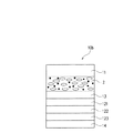
図1は、本発明の一実施形態に係る面光源の概略構成を示す縦断面図である。
図1に示すように、本実施形態に係る面光源10は、電気エネルギーによって発光を取り出す固体発光素子1と、固体発光素子1の光取り出し面側(図1の紙面上側)に実質的に空気層を介することなく形成された異方散乱性色変換層2とを備えている。
【0032】
本実施形態に係る固体発光素子1は、有機エレクトロルミネッセンス素子(有機EL素子)とされており、ガラス基板からなる支持基板11と、正孔輸送層121、発光層122及び電子輸送層123の3層が積層された有機薄膜層12と、有機薄膜層12の両端にそれぞれ形成された透明電極(陽極)13と、金属反射電極(陰極)14とを備えている。斯かる電極13、14間に電圧を印加すると、陽極13からは正孔が、陰極14からは電子が注入され、それぞれ正孔輸送層121及び電子輸送層123を移動し、発光層122で再結合することにより、励起子が発生し、EL発光が得られる。発光した光のうち、上側(図1の紙面上方)に向う光は透明電極13及びガラス基板11を通過し、異方散乱性色変換層2に入射する。一方、下側(図1の紙面下方)に向う光は、陰極14で反射した後、同様にして異方散乱性色変換層2に入射することになる。以上の過程において、屈折率の低い空気層(屈折率=1)が介在しないため、発光層122で発光した光は全反射を受けることなく異方散乱性色変換層2に入射することができる(ただし、透明電極13やガラス基板11の屈折率によっては、一部の光が全反射される場合もある)。なお、本実施形態では、発光効率が良く、低駆動電圧、低消費電力であるという観点から、固体発光素子1として有機EL素子を用いたが、本発明はこれに限るものではなく、分散型無機EL素子や発光ダイオードなど任意の固体発光素子を適用可能である。
【0033】
有機EL素子1に用いられる有機材料、電極材料、層構成、各層の膜厚に関しては、特に制限はなく、従来の有機EL素子を適用することができる。有機薄膜層12は、低分子系の材料を真空蒸着して形成しても良いし、高分子系の材料を塗布等によって形成してもよく、特に制限はない。
【0034】
また、有機EL素子1の層構成としては、本実施形態のように、陽極13/正孔輸送層121/発光層122/電子輸送層123/陰極14とする他、陽極/発光層/陰極や、陽極/正孔輸送層/電子輸送性発光層/陰極などとすることも可能である。その他、陽極界面に正孔注入層や陰極界面に電子注入層を設けたり、再結合効率を高めるために電子ブロック層や正孔ブロック層を挿入した構成としても良い。基本的には、発光効率がより高くなる構成、材料、形成方法を選択することにより、少ない消費電力で強度の発光が得られるため、後述する異方散乱性色変換層2の発光性材料23を効率良く励起発光できる点で好ましい。
【0035】
陽極13や陰極14の電極材料についても適宜最適なものを選択すればよい。
通常の有機EL素子においては、陽極13には酸化インジウム錫(ITO)や酸化錫等の透明導電膜が用いられ、陰極14にはMgとAgをおよそ10:1の原子比で共蒸着したものや、Ca電極、Liを微量ドープしたAl電極などが陰極の低仕事関数化による電子注入効率向上の観点から用いられているが、特にこれに限るものではない。
【0036】
支持基板11としては、透明性の有無に関わらず一般的なものを使用することができる。本実施形態では、前述のように支持基板11としてガラス基板を用い、有機薄膜層12からの発光を透明電極13を介して支持基板11側に取り出す構成であるが、図2に示す面光源10aのように、不透明な金属板を支持基板11aとして用い、透明電極13上に異方散乱性色変換層2を形成する構成しても良い(この場合は、支持基板11aと反対側に光を取り出す構成となる)。また、陽極13を透明電極とする以外に、例えば、有機薄膜層1界面から厚み数nm〜十数nmの透光性を維持し得る厚みの金属電極を形成し、その後、当該金属電極上にITOを形成すること等によって、陰極14を透明電極とすることも可能である(この場合、有機薄膜層12の両面から光を取り出すことができる)。さらには、図3に示す面光源10bのように、ガラス基板からなる支持基板11と透明電極13との間に異方散乱性色変換層2を形成する構成も採用可能である。
なお、図3に示す構成では、異方散乱性色変換層2上(光取り出し面側)にガラス基板が存在することになるが、後述する本発明の効果は同様に発揮される。
【0037】
また、支持基板11として、高分子フィルムを用いることもできる。具体的には、ポリエチレンテレフタレート、ポリエチレンナフタレート、ポリエーテルスルホン、ポリカーボネート、ポリアクリレート、ポリエーテルエーテルケトン、ノルボルネン系樹脂、トリアセチルセルロースなどによって支持基板11を形成することも可能である。ただし、図4に示すように、支持基板11が異方散乱性色変換層2よりも出射面側に形成されている場合、異方散乱性色変換層2によって得られた直線偏光を維持するべく、支持基板11として、複屈折性(光学異方性)を有しないもの(或いは、低いもの)を選択する必要がある。仮に、支持基板11が複屈折性を有すると、異方散乱性色変換層2から出射する直線偏光との間での、その光軸や位相差の関係によっては直線偏光が楕円偏光に変換されるため、液晶表示装置等に適用する際に、偏光板において吸収される成分が増加してしまう場合がある。従って、支持基板11としては、ガラス板、エポキシ樹脂基板、三酢酸セルロースフィルム、ノルボルネン系樹脂フィルムの他、市販の光学異方性を有しないか、或いは、低い基板を用いる必要がある。
【0038】
図1〜図3に示す面光源において、異方散乱性色変換層2は、支持基板11上や透明電極13上に直接形成されているが、透明な粘着剤や接着剤を介して、これらを貼り合わせることにより形成することも可能である。この場合、有機EL素子1からの発光が極力全反射によって失われないようにするべく、各層の屈折率を考慮して、粘着剤や接着剤の屈折率を調整することが好ましい。
【0039】
例えば、図1に示す面光源10において、異方散乱性色変換層2をガラス基板11上に粘着剤を用いて貼着する場合、当該粘着剤の屈折率はガラス基板11の屈折率より高く、且つ、後述する異方散乱性色変換層2の透光性樹脂21の屈折率より小さくしておくことが好ましい。斯かる構成によれば、ガラス基板11/粘着剤、及び粘着剤/異方散乱性色変換層2の界面で全反射は生じず、効率良く異方散乱性色変換層2に発光を入射させることができる。但し、粘着剤の屈折率が必ずしも上記関係を満足していなくても、その屈折率差は0.1程度乃至それ以下であるため、本発明の効果を著しく低下させるおそれはない。
【0040】
ただし、図2に示す面光源10aや図3に示す面光源10bのように、異方散乱性色変換層2を透明電極13上に粘着剤を用いて貼着する場合には注意が必要である。例えば、透明電極として専ら用いられるITOの屈折率は、およそ1.8〜2.0と大きく、アクリル系粘着剤の屈折率は、およそ1.45〜1.5程度であり、比較的屈折率差が大きいので、全反射の影響が無視できなくなる。従って、粘着剤や接着剤の屈折率をITOのように大きくするのは困難であるものの、できるだけその屈折率を高くし、その分、全反射による損失を低減する必要がある。
【0041】
異方散乱性色変換層2は、透光性樹脂21と、透光性樹脂21に分散分布され、透光性樹脂21とは複屈折性の相違する微小領域部22と、透光性樹脂21及び/又は微小領域部22中に含有された少なくとも1種以上の発光性材料23とを具備している(図1では、透光性樹脂21中に発光性材料23を含有している例を図示している)。
【0042】
異方散乱性色変換層2の形状は、少なくとも2面の対向する平坦面を有していれば特に制限はないが、面光源への利用や、全反射効率という観点から、図1に示すように、断面矩形のフィルム状、シート状、或いは、プレート状の形状であることが好ましく、特に、取り扱いが容易である点で、フィルム状に形成することが望ましい。異方散乱性色変換層2の厚みは、好ましくは10mm以下、より好ましくは0.1〜5mm、さらに好ましくは0.4mm〜2mmとされる。
【0043】
異方散乱性色変換層2の対向する2面201、202は、発光性材料23で発光した光を全反射によって閉じこめる閉じ込め効率の観点より、鏡面に近い平滑性を有することが好ましい。ただし、異方散乱性色変換層2の対向する2面201、202の平滑性が乏しい場合には、別途平滑性に優れた透光性のフィルムやシートを透明な接着剤や粘着剤で透光性樹脂21に貼着し、当該貼着した透光性のフィルムやシートの平滑な表面を全反射界面とすることでも同様の効果が得られる。
【0044】
発光性材料23は、透光性樹脂21及び微小領域部22のいずれか一方、又は、両方に均一に溶解又は分散されていることが好ましい。発光性材料23によって光の散乱が生じることは望ましくないため、溶解する材料であることがより好ましい。また、発光性材料23を分散する場合には、不必要な光の散乱を抑制するという観点から、その分散サイズはできる限り小さい方が好ましい。発光性材料23は、例えば、異方散乱性色変換層2の形成の際に、透光性樹脂21や微小領域部22を形成する材料に予め発光材料23を必要に応じて他の添加剤と共に配合しておく方法など、適宜な方法によって溶解又は分散させることができる。
【0045】
発光性材料23としては、紫外光又は可視光を吸収して、可視光領域の波長の光を励起発光する適宜な材料の1種又は2種以上を用いることができ、特に制限はない。より具体的には、励起1重項からの発光である蛍光や3重項からの発光である燐光などを放射する有機染料や無機顔料等からなる蛍光材料や蓄光材料を用いることができる。
【0046】
発光性材料23としては、青色、緑色、赤色の発光波長を有する材料をそれぞれ単独で又は混合して用いることが好ましい。例えば、発光性材料23を有機蛍光染料(青色蛍光体、緑色蛍光体、赤色蛍光体)とする場合について、以下に具体的に説明する。
【0047】
青色蛍光体として好ましい有機化合物は、溶液状態での蛍光ピーク波長が380nm以上480nm未満であれば特に制限はない。具体的には、特開平6−203963号公報に記載されている、スチルベン誘導体、ジスチリルアリーレン誘導体及びトリススチリルアリーレン誘導体の中から選ばれた少なくとも一種を含有させるのが好ましい。その他の好ましい青色蛍光体としては、アントラセン、ペリレン、コロネン等の多環芳香族やそのアルキル置換体が挙げられる。
【0048】
緑色蛍光体として好ましい有機化合物は、溶液状態での蛍光ピーク波長が480nm以上580nm未満であれば特に制限はない。具体的には、緑色蛍光体として、3−(2’−ベンジミダゾリル)−7−N,N−ジエチルアミノクマリン(クマリン535)、3−(2−ベンゾチアゾリル)−7−ジエチルアミノクマリン(クマリン6)、2,3,5,6−1H,4H−テトラヒドロ−8−トリフルオロメチルキノリジノ−<9,9a,1−gh>クマリン(クマリン540A)、3−(5−クロロ−2−ベンゾチアゾリル)−7−ジエチルアミノクマリン(クマリン34)、4−トリフルオロメチル−ピペリジノ[3,2−g]クマリン(クマリン340)、N−エチル−4−トリフルオロメチル−ピペリジノ[3,2−g]クマリン(クマリン355)、N−メチル−4−トリフルオロメチルーピペリジノ[2,3−h]クマリン、9−シアノ−1,2,4,5−3H,6H,10H−テトラヒドロ−1−ベンゾピラノ[9,9a1−gh]キノリジン−10−オン(クマリン337)等のクマリン化合物、2,7−ジクロロフルオレセン等のキサンチン色素、テトラセン、キナクリドン化合物等が挙げられる。
【0049】
赤色蛍光体として好ましい有機化合物は、溶液状態での蛍光ピーク波長が580nm以上650nm以下であれば特に制限はない。具体的には、例えば、欧州公開特許第0281381号公報に記載されている赤色発振レーザー色素として用いられるジシアノメチレンピラン誘導体、ジシアノメチレンチオピラン誘導体、フルオレセイン誘導体、ペリレン誘導体等が挙げられる。
【0050】
これらの有機化合物は、濃度消光を生じないようにするべく、層を形成する有機化合物(透光性樹脂21又は微小領域部22)に対して、0.1〜10モル%、好ましくは0.5〜5モル%の割合で含有させることが必要である。なお、異方散乱性色変換層2の作成プロセスや、使用環境での発光効率の低下を考慮すれば、堅牢性に優れた発光性材料23を用いることが好ましい。
【0051】
異方散乱性色変換層2は、例えばポリマー類や液晶類等の透明性に優れる適宜な材料の1種又は2種以上を、延伸処理等による適宜な配向処理によって複屈折性の相違する領域が形成される組合せで用いて配向フィルムを得る方法など、適宜な方法で形成することができる。前述したように、発光性材料23は、小さなサイズで分散されていることが望ましいため、前記組み合わせる材料の少なくとも一方は、分散される発光性材料23と相溶性良く混和するものであることが好ましい。
【0052】
前記材料の組合せ例としては、ポリマー類と液晶類の組合せ、等方性ポリマーと異方性ポリマーの組合せ、異方性ポリマ一同士の組合せなどが挙げられる。なお、微小領域部22の分散分布性などの点より、相分離する組合せとすることが好ましく、組み合せる材料の相溶性によって分散分布性を制御することができる。例えば、非相溶性の材料を溶媒によって溶液化する方法や、非相溶性の材料を加熱溶融下に混合する方法など、適宜な方法によって相分離させることができる
。
【0053】
前記材料の組合せで延伸処理によって配向処理する場合、ポリマー類と液晶類の組合せ及び等方性ポリマーと異方性ポリマーの組合せでは、任意の延伸温度や延伸倍率によって、異方性ポリマ一同士の組合せでは、延伸条件を適宜に制御することによって、それぞれ目的とする異方散乱性色変換層2を形成することができる。なお、異方性ポリマーは、延伸方向の屈折率変化の特性に基づいて正負に分類されるが、本実施形態では、正負いずれの異方性ポリマーをも用いることができ、正同士の組合せ、負同士の組合せ及び正負の組合せのいずれをも使用することが可能である。
【0053】
前記ポリマー類の例としては、ポリエチレンテレフタレートやポリエチレンナフタレートの如きエステル系ポリマー、ポリスチレンやアクリロニトリル・スチレン共重合体(ASポリマー類)の如きスチレン系ポリマー、ポリエチレン、ポリプロピレン、シクロ系乃至ノルボルネン構造を有するポリオレフィン、エチレン・プロピレン共重合体の如きオレフィン系ポリマー、ポリメチルメタクリレートの如きアクリル系ポリマー、二酢酸セルロースや三酢酸セルロースの如きセルロース系ポリマー、ナイロン(脂肪族ポリアミド)や芳香族ポリアミドの如きアミド系ポリマーが挙げられる。
【0054】
また、カーボネート系ポリマー、塩化ビニル系ポリマー、イミド系ポリマー、スルホン系ポリマー、ポリエーテルスルホン、ポリエーテルエーテルケトン、ポリフェニレンスルフィド、ビニルアルコール系ポリマー、塩化ビニリデン系ポリマー、ビニルブチラール系ポリマー、アリレート系ポリマー、ポリオキシメチレン、シリコーン系ポリマー、ウレタン系ポリマー、エーテル系ポリマー、酢酸ビニル系ポリマー、前記ポリマーの混合物、或いは、フェノール系、メラミン系、アクリル系、ウレタン系、ウレタンアクリル系、エポキシ系、シリコーン系等の熱硬化型又は紫外線硬化型のポリマー類なども前記透明なポリマー類の例として挙げられる。
【0055】
一方、前記液晶類の例としては、シアノビフェニル系、シアノフェニルシクロヘキサン系、シアノフェニルエステル系、安息香酸フェニルエステル系、フェニルピリミジン系、これらの混合物の如き、室温又は高温でネマチック相やスメクチック相を呈する低分子液晶や架橋性液晶モノマーの他、室温又は高温でネマチック相やスメクチック相を呈する液晶ポリマーなどが挙げられる。前記架橋性液晶モノマーは、通常、配向処理した後、熱や光等による適宜な方法で架橋処理されてポリマーとされる。
【0056】
耐熱性や耐久性等に優れる異方散乱性色変換層2を得るという観点では、ガラス転移温度が好ましくは50℃以上、より好ましくは80℃以上、特に好ましくは120℃以上のポリマ一類と、架橋性液晶モノマー又は液晶ポリマーとの組合せを用いることが好ましい。前記液晶ポリマーとしては、主鎖型や側鎖型等の適宜なものを用いることができ、その種類について特に限定はない。粒径分布の均一性に優れる微小領域部22の形成性、熱的安定性、フィルムへの成形性、配向処理の容易性などの点より、液晶ポリマーとして、重合度が好ましくは8以上、より好ましくは10以上、特に好ましくは15〜5000のものを用いるのが好ましい。
【0057】
液晶ポリマーを用いた異方散乱性色変換層2は、例えばポリマ一類の1種又は2種以上と、微小領域部22を形成するための液晶ポリマーの1種又は2種以上を混合して、液晶ポリマーが微小領域を占める状態で分散含有されたポリマーフィルムを形成し、適宜な方法で配向処理し、複屈折性が相違する領域を形成する方法などによって形成することができる。
【0058】
ここで、微小領域部22と透光性樹脂21との屈折率差について、当該屈折率差が最大値を示す微小領域部22の軸方向の屈折率差をΔn1とし、前記最大値を示す軸方向に直交する軸方向の屈折率差をΔn2及びΔn3とする。前記配向処理による屈折率差△n1、△n2及びΔn3の制御性等の点より、前記液晶ポリマーとしては、ガラス転移温度が50℃以上で、併用のポリマー類(透光性樹脂21)のガラス転移温度よりも低い温度域でネマチック液晶相を呈するものを用いるのが好ましい。その具体例としては、下記の一般式で表されるモノマー単位を有する側鎖型の液晶ポリマーなどが挙げられる。
一般式:(−X−)n
|
Y−Z
【0059】
前記一般式において、Xは、液晶ポリマーの主鎖を形成する骨格基であり、線状、分岐状、環状等の適宜な連結鎖によって形成されていればよい。その具体例としては、ポリアクリレート類、ポリメタクリレート類、ポリ−α−ハロアクリレート類、ポリ−α−シアノアクリレート類、ポリアクリルアミド類、ポリアクリロニトリル類、ポリフタクリロニトリル類、ポリアミド類、ポリエステル類、ポリウレタン類、ポリエーテル類、ポリイミド類、ポリシロキサン類などが挙げられる。
【0060】
また、Yは、主鎖より分岐するスペーサ基である。屈折率差の制御など異方散乱性色変換層2の形成性などの点より、スペーサ基Yとしては、例えば、エチレン、プロピレン、ブチレン、ペンチレン、ヘキシレン、オクチレン、デシレン、ウンデシレン、ドデシレン、オクタデシレン、エトキシエチレン、メトキシブチレンなどとするのが好ましい。一方、Zは、液晶配向性を付与するメソゲン基である。
【0061】
前記ネマチック配向性の側鎖型液晶ポリマーは、前記一般式で表されるモノマー単位を有するホモポリマーやコポリマー等の適宜な熱可塑性ポリマーであればよく、特にモノドメイン配向性に優れるものが好ましい。
【0062】
ネマチック配向性の液晶ポリマーを用いた異方散乱性色変換層2は、例えば、ポリマーフィルムを形成するためのポリマー類と、そのポリマー類のガラス転移温度よりも低い温度域でネマチック液晶相を呈し、ガラス転移温度が好ましくは50℃以上、より好ましくは60℃以上、特に好ましくは70℃以上の液晶ポリマーとを混合して、液晶ポリマーが微小領域を占める状態で分散含有されたポリマーフィルムを形成した後、その微小領域部22を形成する液晶ポリマーを加熱処理してネマチック液晶相に配向させ、その配向状態を冷却固定する方法などによって形成することができる。
【0063】
配向処理前の微小領域部22を分散含有するポリマーフィルム(透光性樹脂21)、すなわち、配向処理対象のフィルムは、例えば、キャスティング法、押出成形法、射出成形法、ロール成形法、流延成形法などの適宜な方法によって形成することができる他、モノマー状態で展開し、それを加熱処理や紫外線等の放射線処理などにより重合してフィルム状に製膜する方法などによっても形成することができる。
【0064】
微小領域部22の均等分布性に優れる異方散乱性色変換層2を得るという点では、溶媒を介した形成材の混合液をキャスティング法や流延成形法等によって製膜する方法が好ましい。その場合、溶媒の種類、混合液の粘度、混合液展開層の乾燥速度などによって微小領域部22の大きさや分布性などを制御することができる。微小領域部22の小面積化には、混合液の低粘度化や混合液展開層の乾燥速度の急速化などが有効である。
【0065】
配向処理対象のフィルムの厚みは、適宜に決定すればよいが、一般には、配向処理性などの点より、好ましくは1μm〜3mm、より好ましくは5μm〜1mm、特に好ましくは10〜500μmとされる。なお、フィルムの形成に際しては、例えば、分散剤、界面活性剤、色調調節剤、難燃剤、離型剤、酸化防止剤などの適宜な添加剤を配合することができる。
【0066】
配向処理は、例えば、1軸、2軸、逐次2軸、Z軸等による延伸処理方法、圧延方法、ガラス転移温度又は液晶転移温度以上の温度で電場又は磁場を印加して急冷し配向を固定化する方法、製膜の際に流動配向させる方法、等方性ポリマーの僅かな配向に基づいて液晶を自己配向させる方法など、配向によって屈折率を制御し得る適宜な方法の1種又は2種以上を用いて行うことができる。従って、得られる異方散乱性色変換層2としては、延伸フィルムとなる場合もあるし、非延伸フィルムとなる場合もある。なお、延伸フィルムとする場合、脆性ポリマーを用いることもできるが、延び性に優れるポリマーを用いるのが好ましい。
【0067】
また、微小領域部22が液晶ポリマーからなる場合には、例えば、ポリマーフィルム中に分散分布する液晶ポリマーがネマチック液晶相等の目的とする液晶相を呈する温度に加熱して溶融させ、それを配向規制力の作用下に配向させて急冷し、配向状態を固定化する方法などによっても配向処理することができる。微小領域部2の配向状態は、光学特性のバラツキ防止などの観点より、モノドメイン状態にあることが好ましい。
【0068】
なお、前記配向規制力としては、例えば、ポリマーフィルムを適宜な倍率で延伸処理する方法による延伸力、フィルム形成時のシェアリングカ、電界や磁界など、液晶ポリマーを配向させることができる適宜な規制力を適用でき、その1種又は2種以上の規制力を作用させて、液晶ポリマーを配向処理することができる
。
【0070】
異方散乱性色変換層2における微小領域部22以外の部分、つまり透光性樹脂21は、複屈折性を示すものであってもよいし、等方性のものであってもよい。
異方散乱性色変換層2の全体が複屈折性を示すものは、フィルム形成用のポリマー類として配向複屈折性のものを用いて、前述した製膜過程における分子配向などによって得ることができる。なお、必要に応じて、例えば、延伸処理等の公知の配向処理を施し、複屈折性を付与乃至制御することも可能である。また、微小領域部22以外の部分が等方性の異方散乱性色変換層2は、例えば、フィルム形成用のポリマー類として等方性のものを用いて、そのフィルムを当該ポリマー類のガラス転移温度以下の温度領域で延伸処理する方法などによって得ることができる。
【0069】
前述のように、透光性樹脂21と微小領域部22とは複屈折性が相違している。具体的には、前述のように、微小領域部22と透光性樹脂21との屈折率差について、当該屈折率差が最大値を示す微小領域部22の軸方向(Δn1方向)の屈折率差をΔn1とし、前記最大値を示す軸方向に直交する軸方向(Δn2方向、Δn3方向)の屈折率差をΔn2及びΔn3とした場合、後述する全反射の点より、Δn1は適度に大きいことが好ましく、Δn2及びΔn3は小さければ小さいほど良く、できるだけゼロであることが好ましい。本実施形態に係る異方散乱性色変換層2は、0.03≦Δn1≦0.5、0≦Δn2≦0.03、0≦Δn3≦0.03となるように制御されており、より好ましくは、さらにΔn2=Δn3とされる。なお、斯かる屈折率差は、使用材料の屈折率や配向処理などによって制御することができる。
【0070】
斯かる屈折率差Δn1、Δn2及びΔn3とすることにより、異方散乱性色変換層2内部に入射した励起光によって励起発光した光の内、△n1方向の直線偏光が強く散乱され、臨界角(全反射角)よりも小さい角度で散乱されることにより異方散乱性色変換層2から外部に出射する光量を増やすことができる一方、それ以外の方向の直線偏光は散乱され難く、全反射を繰り返すことにより、異方散乱性色変換層2の内部に閉じ込めることができる。
【0071】
なお、微小領域部22の各軸方向と透光性樹脂21との屈折率差(Δn1、Δn2及びΔn3)は、透光性樹脂21が光学的等方性のものである場合には、微小領域部22の各軸方向の屈折率と透光性樹脂21の平均屈折率との差を意味し、透光性樹脂21が光学的異方性のものである場合には、透光性樹脂21の主光軸方向と微小領域部22の主光軸方向とが通常は一致しているため、それぞれの軸方向における各屈折率の差を意味する。
【0072】
△n1方向は、異方散乱性色変換層2から出射される直線偏光の振動面に平行であるため、斯かる△n1方向は異方散乱性色変換層2の対向する2面201、202に平行であることが好ましい。なお、2面201、202に平行である限り、△n1方向は、面光源10を適用する液晶セル等に応じた適宜な方向とすることができる。
【0073】
異方散乱性色変換層2における微小領域部22は、当該微小領域部22における散乱効果の均質性などの点より、できるだけ均等に分散分布していることが好ましい。微小領域部22の大きさ、特に散乱方向である△n1方向の長さは、後方散乱(反射)や波長依存性に影響する。光利用効率の向上、波長依存性による着色の防止、微小領域部22の視覚化による視認阻害の防止ないし鮮明な表示の阻害防止、さらには製膜性やフィルム強度などの点より、微小領域部22の好ましい大きさ、特に△n1方向の長さは、好ましくは0.05〜500μm、より好ましくは0.1〜250μm、特に好ましくは1〜100μmである。なお、微小領域部22は、通常、ドメインの状態で異方散乱性色変換層2内に存在するが、その△n2方向等の長さについては特に限定はない。
【0074】
異方散乱性色変換層2中に占める微小領域部22の割合は、△n1方向の散乱性などの点より適宜に決定することができるが、一般には、フィルム強度なども踏まえ、好ましくは0.1〜70重量%、より好ましくは0.5〜50重量%、特に好ましくは1〜30重量%とされる。
【0075】
本実施形態に係る異方散乱性色変換層2は、単層で形成することができる他、2層以上を重畳したものとして形成することも可能である。当該異方散乱性色変換層2の重畳化により、厚み増加以上の相乗的な散乱効果を発揮させることができる。斯かる重畳体は、散乱効果を増加させる等の点より、△n1方向が各層で平行関係となるように重畳したものが好ましい。重畳数は、2層以上の適宜な数とすればよい。
【0076】
重畳する異方散乱性色変換層2は、△n1、△n2及びΔn3が互いに同じものであっても良いし、異なるものであっても良い。また、各異方散乱性色変換層2に含まれる発光性材料23についても、同じ材料であっても異なる材料であっても良い。なお、△n1方向等についての各層での平行関係は、前述のように互いに平行であることが好ましいものの、作業誤差によるズレなどは許容される。
また、各異方散乱性色変換層2内で△n1方向等にバラツキがある場合には、その平均方向が平行関係となるように重畳するのが好ましい。
【0077】
異方散乱性色変換層2は、当該異方散乱性色変換層2内を光が伝送する過程で、適当に偏光状態が解消される必要があることから、異方散乱性色変換層2全体で又は部分的に位相差を有するように構成することが好ましい。なお、基本的には異方散乱性色変換2の遅相軸(Δn1方向の軸)と、散乱されにくい直線偏光の偏光軸(振動面)とは直交関係にあるため、位相差による偏光変換は生じ難いものの、僅かな散乱によって見かけの角度が変化し、偏光変換が生じるものと考えられる。
【0078】
斯かる偏光変換を生じさせる点より、一般には異方散乱性色変換層2が5nm以上の面内位相差を有することが好ましいが、当該異方散乱性色変換層2の厚みに応じてその値は変化する。なお、斯かる位相差は、異方散乱性色変換層2に複屈折性の微粒子を含有させる方法や表面に付着させる方法、透光性樹脂21を複屈折性とする方法、それらを併用する方法の他、複屈折性フィルムを一体化積層する方法等、適宜な方法で付与することができる。
【0079】
本実施形態に係る面光源10において、異方散乱性色変換層2からの光の取り出し面側(上面側)には、偏光維持性のレンズシートや光拡散層を配置することができる他、波長カットフィルターや位相差フィルムなどを適宜配置することも可能である。
【0080】
レンズシートは、面光源10からの出射光(直線偏光)を、その偏光度を維持しつつ光路制御し、視認に有利な正面方向への指向性を向上させ、散乱性の出射光の強度ピークを正面方向とすることなどを目的として配置される。
【0081】
波長カットフィルターは、有機EL素子1からの直接光が、本実施形態に係る面光源10で照明される液晶表示素子などに進入することを防止する目的で配置される。特に、励起光が紫外線である場合には、紫外線による液晶や偏光板の劣化を防止する必要があるため、波長カットフィルターが好適に用いられる。また、波長カットフィルターは、不必要な波長の可視光線を排除する目的で用いることもできる。なお、波長カットフィルターを別途設けず、異方散乱性色変換層2やその他の光学部材に例えば紫外線吸収剤などを配合して波長カットの機能をもたせることも可能である。
【0082】
以上に説明したように、本実施形態に係る面光源10は、有機EL素子1より入射した光を用いて、異方散乱性色変換層2から直線偏光として出射し得ると共に、その偏光方向(振動面)を制御可能であり、さらには、発光性材料23を適宜選択することにより、直線偏光の発光色を任意に設定可能(複数の発光性材料23を添加し、その添加量を調整することにより、白色発光を得ることも可能)であるため、例えば、液晶表示装置など直線偏光を利用する種々の装置や用途に好適に用いることができる。
【0083】
なお、本発明に係る面光源は、図4に示すように、固体発光素子1と、固体発光素子1の光取り出し面側(図4の紙面上側)に実質的に空気層を介することなく形成された異方性散乱層2aと、固体発光素子1の有機薄膜層12(特に発光層)と異方性散乱層2aとの間に形成され、少なくとも1種以上の発光性材料を含有する色変換層2bとを備えた構成とすることも可能である。換言すれば、異方性散乱層2aと発光性材料(色変換層2b)とを別個に設ける構成とすることも可能である。
【0084】
異方性散乱層2aは、前述した異方散乱性色変換層2に発光性材料23を分散させずに作製すればよい。また、色変換層2bは、例えば、透明な樹脂に前述した発光性材料23を分散させて形成しても良いし、基板11自体に発光性材料23を含有させる(つまり、この場合には基板11自体が色変換層2bの役割を兼ねることになる)ことも可能である。ここで、有機薄膜層12の発光層と色変換層2bとの間、色変換層2bと異方性散乱層2aとの間は、空気層を介することなく形成される。従って、図4に示す面光源10cも、色変換層2bで発生した励起発光が全反射することなく異方性散乱層2aに入射するため、図1に示す面光源10と同様の作用効果を発揮することができる。なお、異方性散乱層2aの代わりに前述した異方散乱性色変換層2を用い、これを前記色変換層2bと組み合わせる構成を採用することも可能である。
【0085】
【実施例】
以下、実施例及び比較例を示すことにより、本発明の特徴をより一層明らかにする。
【0086】
<実施例1>
(1)有機EL素子の作製
ガラス基板の片側にITOセラミックターゲット(In2O3:SnO2=90重量%:10重量%)から、DCスパッタリング法を用いて、厚み100nmのITO膜からなる透明電極(陽極)を形成した。その後、フォトレジストを用いてITO膜をエッチングすることにより、発光面積が15mmX15mmとなるようにパターンを形成した。次に、超音波洗浄を行った後、低圧UVランプを用いてオゾン洗浄した。次に、ITO面上に、真空蒸着法によって、下記の条件で有機薄膜層を順次形成した。すなわち、
・正孔注入層としてCuPc(下記の化学式1)を、蒸着速度0.3nm/sで15nm形成し、
【化1】

【化2】
【化3】
その後、Mgを1nm/s、Agを0.1nm/sの蒸着速度で共蒸着し、厚み100nmのMgAg層を形成した後、MgAg層の酸化防止の観点から、さらにその上にAgを50nm形成して陰極電極とした。次に、真空蒸着装置から取り出した後、陰極電極側に紫外線硬化性エポキシ樹脂を滴下し、その上にスライドガラスを被せ、十分に工ポキシ樹脂が広がった時点で、高圧∪∨ランプを用いてエポキシ樹脂を硬化させて、素子を封止した。
【0088】
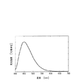
以上のようにして作製した有機EL素子に10Vの直流電圧を印加したところ、31.2mA(電流密度9.63mA/cm2)の電流が流れ、青色のEL発光が得られた。正面輝度を輝度計(トプコン社製、商品名BM9)で測定したところ、46cd/m2であった。また、図5には、作製した有機EL素子の発光スペクトルを瞬間マルチ測光システム(大塚電子社製、商品名MCPD3000)によって測定した結果を示す。なお、作製した有機EL素子において、電圧印加後、時間とともに輝度が低下する傾向が見られたので、本実施例1及び後述する他の実施例及び比較例の輝度測定は全て、電圧を印加してから2秒後の値を採用することで統一した。
【0089】
(2)異方散乱性色変換層の作製
ノルボルネン系樹脂(JSR社製、アートン、ガラス転移温度182℃)950部(重量部、以下同じ)、下記の化学式4で表される液晶ポリマー(ガラス転移温度80℃、ネマチック液晶化温度100〜290℃)50部、下記の化学式5で表される3−(2−ベンゾチアゾリル)−7−ジエチルアミノクマリン(クマリン6)2部を溶解させた20重量%ジクロロメタン溶液を用いてキャスト法により厚み100μmのフィルムを形成し、それを180℃で3倍に延伸処理したのち急冷して異方散乱性色変換層をフィルム形態で形成した。
【化4】
前記異方散乱性色変換層は、ノルボルネン系樹脂からなる透明フィルム中に液晶ポリマーが延伸方向に長軸な状態でほぼ同じ形状のドメイン状に分散したものであり、屈折率差△n1が0.23で、△n2及び△n3がそれぞれ0.029であった。なお、斯かる屈折率差の測定に際しては、ノルボルネン系樹脂を単独で上記と同条件により延伸処理したものと、前記液晶ポリマーを単独で配向膜上に塗布し配向固定したものとについて、それぞれアッベ屈折率計により屈折率を測定し、それらの差を前記Δn1、Δn2及びΔn3として算出した。クマリン6は、ノルボルネン系樹脂に溶解した形で存在していた。また、微小領域部(液晶ポリマーのドメイン)の平均径を偏光顕微鏡観察による位相差に基づく着色によって測定したところ、△n1方向の長さが約5μmであった。
【0091】
(3)有機EL素子への異方散乱性色変換層の形成
前記(2)のようにして作製した異方散乱性色変換層(フィルム)を、前記(1)のようにして作製した有機EL素子のガラス基板上に、アクリル系透明粘着剤層(厚み25μm)を介して貼着した。この状態で、有機EL素子に10Vの電圧を印加したところ、前記(1)で述べたのと略同じ電流が流れ、図6に示すようにクマリン6からの緑色の発光が得られた。また、そのときの輝度は146cd/m2であった。
【0092】
(4)偏光板の設置
上記(3)で作製した面光源の異方散乱性色変換フィルムの延伸方向と、偏光板(日東電工社製、NPF−SEG1425DU)の透過軸とが平行となるように、当該偏光板を異方散乱性色変換フィルム上に設置した。有機EL素子に10Vの電圧を印加したところ、そのときの輝度は91cd/m2であった。また、異方散乱性色変換フィルムの延伸方向と、偏光板の透過軸とが直交するように、当該偏光板を設置した場合について、同様の測定を行ったところ、そのときの輝度は47cd/m2であった。つまり、本実施例に係る面光源からは、異方散乱性色変換フィルムの延伸方向に電界が振動する直線偏光成分に富む偏光が出射していることが分かった。
【0093】
<比較例1>
上記実施例1の(2)異方散乱性色変換層の作製において、キャスト法により厚み100μmのフィルムを形成した後、それを延伸処理せずに、色変換層をフィルム形態で形成した。当該色変換フィルムを実施例1と同様に有機EL素子のガラス基板上に、アクリル系透明粘着剤層を介して貼着した。この状態で、有機EL素子に10Vの電圧を印加したところ、実施例1の場合と略同じ電流が流れ、図6に示すようにクマリン6からの緑色の発光が得られた。また、そのときの輝度は141cd/m2であった。
【0094】
本比較例の色変換フィルム上に偏光板を設置したところ、輝度は61cd/m2であり、偏光板をどの方向に設置しても、輝度は略同じ値であった。つまり、本比較例に係る面光源からは、偏りのない自然光が出射していることが分かった。
【0095】
<比較例2>
上記実施例1の(2)異方散乱性色変換層の作製において、化学式4で表される液晶ポリマーを添加せず、化学式5で表わされる3−(2−ベンゾチアゾリル)−7−ジエチルアミノクマリン(クマリン6)2部を溶解させた20重量%ジクロロメタン溶液を用いてキャスト法により厚み100μmのフィルムを形成した後、それを延伸処理せずに、単なる色変換層をフィルム形態で形成した。当該色変換フィルムは、実施例1の異方散乱性色変換層や比較例1の色変換層とは異なり、光散乱のない透き通ったフィルムであった。この色変換フィルムを実施例1と同様に有機EL素子のガラス基板上に、アクリル系透明粘着剤層を介して貼着した。この状態で、有機EL素子に10Vの電圧を印加したところ、図6に示すようにクマリン6からの緑色の発光が得られた。また、そのときの輝度は103cd/m2であった。
【0096】
本比較例の色変換フィルム上に偏光板を設置したところ、輝度は44cd/m2であり、偏光板をどの方向に設置しても、輝度は略同じ値であった。つまり、本比較例に係る面光源からは、偏りのない自然光が出射していることが分かった。
【0097】
<比較例3>
上記実施例1の(3)において、異方散乱性色変換フィルムを有機EL素子のガラス基板上に形成する際、アクリル系透明粘着剤層も用いず、空気層を介してガラス基板上に載置するようにして設置した。この状態で、有機EL素子に10Vの電圧を印加したところ、図6に示すようにクマリン6からの緑色の発光が得られた。また、そのときの輝度は85cd/m2であった。
【0098】
さらに、上記実施例1の(4)と同様に、異方散乱性色変換フィルムの延伸方向と、偏光板の透過軸とが平行となるように、当該偏光板を設置し、有機EL素子に10Vの電圧を印加したところ、そのときの輝度は61cd/m2であった。また、異方散乱性色変換フィルムの延伸方向と、偏光板の透過軸とが直交するように設置した場合について、同様の測定を行ったところ、そのときの輝度は26cd/m2であった。つまり、本比較例に係る面光源からは、異方散乱性色変換フィルムの延伸方向に電界が振動する直絹偏光成分に富む偏光が出射していることが分かった。
【0099】
<実施例2>
上記実施例1の(2)異方散乱性色変換層の作製において、化学式5で表わされる3−(2−ベンゾチアゾリル)−7−ジエチルアミノクマリン(クマリン6)を添加しなかった以外は、実施例1と同様の方法で、異方散乱性フィルムを作製した。次に、実施例1と同様の方法で作製した有機EL素子のガラス基板上に、比較例2で作製した散乱性のない透明な色変換フィルムを、アクリル系透明粘着剤層を介して貼着した後、更に前記異方散乱性フィルムを前記色変換フィルム上に、アクリル系透明粘着剤層を介して貼着した。
【0100】
この状態で、有機EL素子に10Vの電圧を印加したところ、図6に示すようにクマリン6からの緑色の発光が得られた。また、そのときの輝度は140cd/m2であった。
【0101】
さらに、上記実施例1の(4)と同様に、異方散乱性フィルムの延伸方向と、偏光板の透過軸とが平行となるように、当該偏光板を設置し、有機EL素子に10Vの電圧を印加したところ、そのときの輝度は78cd/m2であった。また、異方散乱性フィルムの延伸方向と、偏光板の透過軸とが直交するように設置した場合について、同様の測定を行ったところ、そのときの輝度は52cd/m2であった。つまり、本実施例に係る面光源からは、異方散乱性フィルムの延伸方向に電界が振動する直線偏光成分に富む偏光が出射していることが分かった。
【0102】
<評価>
表1に、実施例1及び実施例2並びに比較例1〜比較例3の特性値を纏めた。
なお、表1において、「延伸軸//透過軸」の項目は、異方散乱性色変換フィルム(又は異方散乱性フィルム)の延伸軸方向と偏光板の透過軸とが平行となるように偏光板を設置した場合の輝度値を示し、「延伸軸⊥透過軸」の項目は、両者が直交するように偏光板を設置した場合の輝度値を示す。また、延伸処理を行わず、出射光が自然光となっている場合(比較例1及び比較例2)には、偏光板を設置した際の輝度値を示している。
【表1】
表1に示すように、実施例1の面光源は、有機EL素子の発光層から放射される励起光(青色発光)が、異方散乱性色変換層に分散されたクマリン6に吸収され、クマリン6からの蛍光発光が得られる際、発光層と色変換層との間に空気層がなく、本来なら全反射される導波光成分も色変換層に取り込まれるため、効率良く有機EL素子からの励起光を利用できる。しかも、クマリン6は、異方散乱性を有する樹脂層中に分散されている為、外部に出射する蛍光発光は、所定の直線偏光成分に富む偏光として取り出される。従って、実施例1の面光源を例えば液晶表示装置用のバックライトとして用いた場合には、偏光板での吸収損失を低減することができ、高効率な面光源が提供されることになる。
【0104】
同様にして、実施例2の面光源は、実施例1と比較すると、やや効率は低下しているものの、ほぼ同様の効果を奏することが分かる。
【0105】
これに対し、延伸処理を施していない色変換フィルムを用いた比較例1の面光源は、色変換フィルムが散乱性を有するものの、複屈折性の相違する微小領域部を有さないため、異方散乱性を付与されていない。その結果、偏光板を設置する前は実施例1と同様の輝度値が得られるが、偏光板を設置することで、50%以上の出射光が偏光板に吸収され輝度が半減してしまうことが分かる。
【0106】
また、色変換層として散乱性のない透明なフィルムを用いた比較例2の面光源は、有機EL素子からの励起光は、色変換層に取り込むことができるものの、当該色変換層で発生した蛍光発光が空気層に出射しようとする際に全反射を受けるため、輝度値が低くなってしまうことが分かる。
【0107】
また、異方散乱性色変換フィルムと有機EL素子との間に、空気層が介在する比較例3の面光源は、偏光出射特性は得られているものの、有機EL素子からの励起光が前記空気層界面で全反射を受け、異方散乱性色変換フィルムに入射せずに、導波光として損失するため、輝度値が低くなっていることが分かる。
【0108】
なお、以上に説明した実施例1及び実施例2には、クマリン6独特の緑色発光のみを例示したが、その他の数種類の発光性材料を適宜添加することにより、白色発光を得ることも可能であり、この場合も同様に、本発明の効果を奏することができる。
【0109】
また、実施例1及び2で作製した有機EL素子、すなわち励起光源として用いた青色発光素子自体は、必ずしも発光効率の高いものではない。しかしながら、前述したように、3重項励起子を利用した燐光からも発光が生じる発光材料や、ダブルヘテロ構造などを用いて、励起光源自体を高効率化すれば、本発明に係る面光源もそれに比例して高効率化されるものである。
【0110】
【発明の効果】
以上に説明したように、本発明に係る面光源によれば、従来のようにマイクロレンズや反射ドット等からなる特別の光出射手段を設ける必要が無く、入射した励起光によって異方散乱性色変換層内部(発光性材料)で発光した光を、所定の振動面を有する直線偏光として効率良く外部に出射することが可能である。これは、固体発光素子の動作電圧や素子電流を低減でき、素子寿命を大幅に向上させることができるという利点にも通じる。また、異方散乱性色変換層の設置角度に応じて直線偏光の偏光方向(振動面)を任意に設定可能である。さらに、外部に出射する直線偏光の発光色は、発光性材料を適宜選択することにより任意に設定できるという優れた効果を奏するものである。
【図面の簡単な説明】
【図1】図1は、本発明の一実施形態に係る面光源の概略構成を示す縦断面図である。
【図2】図2は、本発明の他の実施形態に係る面光源の概略構成例を示す縦断面図である。
【図3】図3は、本発明のさらに他の実施形態に係る面光源の概略構成例を示す縦断面図である。
【図4】図4は、本発明のさらに他の実施形態に係る面光源の概略構成例を示す縦断面図である。
【図5】図5は、本発明の一実施例に係る面光源に適用した有機EL素子の発光スペクトルを示すグラフである。
【図6】図6は、本発明の一実施例に係る面光源の発光スペクトルを示すグラフである。
【符号の説明】
1…固体発光素子(有機EL素子) 2…異方散乱性色変換層
2a…異方性散乱層 2b…色変換層
10,10a,10b,10c…面光源 21…透光性樹脂
22…微小領域部 23…発光性材料[0001]
TECHNICAL FIELD OF THE INVENTION
The present invention relates to a surface light source and a display device using the same, and more particularly, to a translucent light having anisotropic scattering characteristics using light emitted from a solid-state light emitting element such as an organic electroluminescence element (organic EL element) as excitation light. Surface light source capable of emitting natural light extracted from a solid-state light-emitting element as partial polarized light in another wavelength region rich in a predetermined linearly polarized light component by causing a light-emitting material contained in a conductive resin or the like to emit light, and using the same. High efficiency display device.
[0002]
[Prior art]
An electroluminescent element (EL element) or a light emitting diode which emits light by applying a voltage to the light emitting layer between electrodes is used not only as a display device, but also as a planar light source, a light source for an optical fiber, a liquid crystal. Research and development are being actively pursued as various light sources such as display backlights, liquid crystal projector backlights, and display devices. Among them, the organic EL element is particularly excellent in light emission efficiency, low voltage driving, light weight, and low cost, and is an element that has attracted considerable attention in recent years. The biggest concern when using these solid-state light-emitting devices as a light source is to improve the luminous efficiency. For the purpose of obtaining luminous efficiency comparable to that of fluorescent lamps, the structure, materials, driving method, manufacturing method, etc. of the device are required. Various improvements have been studied.
[0003]
However, in a solid-state light-emitting element that extracts light from the light-emitting layer itself, such as an EL element, of the emitted light, a critical angle determined by the refractive index of the light-emitting layer and the refractive index of the emission medium (for example, an air layer) or more. May be totally reflected at the interface between the light-emitting layer and the emission medium, may be confined inside the light-emitting layer, and cannot be extracted to the outside. Here, assuming that the refractive index of the light emitting layer is n, of the light generated in the light emitting layer, the light extraction efficiency η that is extracted to the outside is η = 1 / (2 · nTwo) Is known. For example, when the refractive index of the light emitting layer is 1.7, η ≒ about 17%, and about 80% or more of the light becomes guided light toward the side of the device and is lost as loss light.
[0004]
In the case of an organic EL device, among excitons generated by recombination of electrons and holes injected from an electrode, the probability of generation of a singlet exciton that contributes to light emission is 1/4. The luminous efficiency of the entire system is extremely low, that is, 5% or less, even if only consideration is given. However, in recent years, as a method for increasing the luminous efficiency (quantum efficiency) of the luminescent layer itself, for example, a luminescent material that emits light from phosphorescence using triplet excitons has been developed, and quantum efficiency has been dramatically increased. The possibility of increasing is found (for example, refer to Patent Document 1).
[0005]
However, even if the luminous efficiency (quantum efficiency) of the light emitting layer itself is improved, there is a problem that if the extraction efficiency is low, the overall luminous efficiency obtained by multiplying the quantum efficiency by the extraction efficiency is reduced. In other words, if the extraction efficiency is improved, there is room for the luminous efficiency to be dramatically improved as a synergistic effect.
[0006]
As a method of improving the extraction efficiency, for example, a method of improving the extraction efficiency by making the substrate constituting the EL element itself have a light-collecting property (for example, see Patent Document 2), or a method of forming a light-emitting layer into a discotic liquid crystal (See, for example, Patent Document 3), a method of forming an electrode constituting an EL element in a concave shape (see, for example, Patent Document 4), EL Various methods have been proposed, such as a method of forming an inclined surface on an electrode constituting an element (for example, see Patent Document 5) and a method of forming a diffraction grating or the like on an electrode constituting an EL element (for example, see Patent Document 6). Have been. However, these proposals have problems such as the EL element having a complicated configuration and the luminous efficiency of the light emitting layer itself being deteriorated.
[0007]
Further, as a relatively simple method for improving the extraction efficiency, a method of forming a light diffusion layer on an EL element to diffuse light and reduce light satisfying a total reflection condition can be cited. . Such a method includes, for example, a diffusion plate in which particles having a refractive index distribution structure different in refractive index between the inside and the surface are dispersed and contained in a transparent base material (for example, see Patent Document 7), In addition, a diffusion member provided with a light diffusion layer containing light-transmitting particles arranged in a single-particle layer shape (see, for example, Patent Document 8) can be used, and scattering into the same material as a light-emitting layer of an EL element can be used. Various proposals have been made, such as a method of dispersing particles (for example, see Patent Document 9). These proposals are characterized by the characteristics of the scattering particles, the difference in the refractive index from the dispersion matrix, the dispersion form of the particles, the location where the light diffusion layer is formed, and the like.
[0008]
When the solid-state light-emitting element is used as a backlight for a liquid crystal display device, light emitted from the element is natural light having almost no polarization characteristics. It needs to be converted to linearly polarized light. Therefore, there is a problem that the light utilization efficiency cannot exceed 50% because light absorption loss occurs due to the polarizing plate.
[0009]
As a method for solving such a problem, for example, a method has been proposed in which an organic EL element is formed on an alignment film, and light emitted from the organic EL element itself is extracted as linearly polarized light (for example, see Patent Document 10). According to such a method, although the absorption loss in the polarizing plate of the liquid crystal display device can be reduced to half at the maximum, there is a possibility that the luminous efficiency (quantum efficiency) of the organic EL element is reduced due to the insertion of the alignment film or the like. is there. Further, the point that the light emitted from the organic EL element becomes guided light toward the side of the element due to total reflection and is lost as loss light is the same as in the related art.
[0010]
On the other hand, a color conversion method using a light-emitting material that absorbs light emitted from an organic EL layer and emits fluorescence in a visible light region as a filter has been proposed (for example, see
[0011]
Therefore, guided light can be extracted to some extent by dispersing particles having a different refractive index from the matrix in the matrix in which the luminescent material is dispersed, or by forming a light diffusion layer or a lens sheet on the top. It is possible. However, when the organic EL element provided with such means is used as a backlight of a liquid crystal display device, there is a problem that the absorption loss by the polarizing plate cannot be reduced.
[0012]
Further, a method has been proposed in which light emitted from an organic EL element is emitted through a polarization scattering film (for example, see Patent Document 13). According to such a method, light lost as guided light is extracted by light scattering, and the emitted light is extracted as light rich in linearly polarized light components, so that absorption loss in the polarizing plate of the liquid crystal display device can be reduced. It has the advantage that. However, there is no disclosure or suggestion about the above-described color conversion method, and there is a problem that it is not suitable for use such as performing full-color display.
[0013]
As described above, conventionally, light that is confined as guided light inside a solid-state light emitting element and lost as loss light is effectively extracted, and when used as a backlight of a liquid crystal display device, the absorption loss of a polarizing plate is reduced. At present, there has been no proposal of a surface light source capable of extracting a desired light emission by color conversion.
[0014]
[Patent Document 1]
JP 2001-313178 A
[Patent Document 2]
JP-A-63-314795
[Patent Document 3]
JP-A-10-321371
[Patent Document 4]
JP-A-11-214162
[Patent Document 5]
JP-A-11-214163
[Patent Document 6]
JP-A-11-283751
[Patent Document 7]
JP-A-6-347617
[Patent Document 8]
JP 2001-356207 A
[Patent Document 9]
JP-A-6-151061
[Patent Document 10]
JP-A-11-316376
[Patent Document 11]
JP-A-3-152897
[Patent Document 12]
JP-A-5-258860
[Patent Document 13]
JP-A-2001-203074
[0015]
[Problems to be solved by the invention]
The present invention has been made in order to solve the problems of the related art, and takes out loss light that has been confined as guided light inside the solid-state light-emitting element, and obtains emission light composed of linearly polarized light. To provide a high-luminance surface light source whose polarization direction (vibration surface) can be arbitrarily controlled and can take out any light emission by color conversion, and a display device which is highly efficient and consumes less power by using the same. Issues and
[0016]
[Means for Solving the Problems]
In order to solve the above-mentioned problem, the present invention provides a solid-state light-emitting element for extracting light emission by electric energy and a light-emitting surface side of the solid-state light-emitting element substantially without an air layer, as described in
[0017]
According to the first aspect of the present invention, the anisotropic scattering color conversion layer is formed on the light extraction surface side of the solid state light emitting element without substantially interposing an air layer having a low refractive index (refractive index = 1). Therefore, the light emitted from the solid state light emitting element enters the anisotropic scattering color conversion layer without being totally reflected. Light incident on the anisotropic scattering color conversion layer becomes excitation light of the luminescent material, and the luminescent material absorbs the excitation light and emits fluorescence or phosphorescence. Note that the emission color of fluorescence or phosphorescence can be arbitrarily selected by changing the type of the light-emitting material.
[0018]
Most of the light emitted by excitation in the anisotropic scattering color conversion layer is totally reflected at the air interface according to the refractive index difference between the anisotropic scattering color conversion layer and air, and is reflected in the anisotropic scattering color conversion layer. Transmitted. Among such transmission light, a linearly polarized light component having a vibration plane parallel to the axial direction (Δn1 direction) of the minute region where the refractive index difference between the minute region and the translucent resin shows the maximum value (Δn1) is obtained. It will be strongly scattered selectively. Of such scattered light, light scattered at an angle smaller than the total reflection angle is emitted to the outside (air) from the anisotropic scattering color conversion layer.
[0019]
Here, considering the case where the minute regions are not dispersed and distributed in the translucent resin, since the selective polarization scattering as described above does not occur, the light is excited by the luminescent material in the anisotropic scattering color conversion layer. About 80% of the emitted light is in a state of being confined in the translucent resin and repeating total reflection due to the solid angle.
[0020]
According to the first aspect of the present invention, the confined light is scattered at the interface between the microscopic region and the light-transmitting resin, so that the light outside the anisotropically scatterable color conversion layer only when the total reflection condition is broken. Therefore, the emission efficiency can be arbitrarily controlled depending on the size and distribution ratio of the minute region.
[0021]
On the other hand, the light scattered at an angle larger than the total reflection angle in the scattering in the Δn1 direction, the light not colliding with the minute area portion, and the light having a vibration surface other than the Δn1 direction are anisotropically scattered color conversion layers. And is transmitted while repeating total reflection. The polarization state is also canceled by the birefringence phase difference and the like in the anisotropic scattering color conversion layer, and the condition of the Δn1 direction is satisfied. (In the form of linearly polarized light). By repeating the above operations, as a result, linearly polarized light having a predetermined vibration surface is efficiently emitted from the anisotropic scattering color conversion layer. That is, light originally confined as guided light can be extracted as linearly polarized light.
[0022]
As described above, according to the first aspect of the present invention, it is not necessary to provide a special light emitting means such as a microlens or a reflective dot unlike the related art, and the anisotropic scattering color conversion layer can be formed by the incident excitation light. Light emitted inside (light-emitting material) can be efficiently emitted to the outside as linearly polarized light having a predetermined vibration surface. This leads to the advantage that the operating voltage and the device current of the solid state light emitting device can be reduced, and the life of the device can be greatly improved. Further, the polarization direction (vibration plane) of the linearly polarized light can be arbitrarily set according to the installation angle of the anisotropic scattering color conversion layer (depending on the Δn1 direction). Further, the emission color of linearly polarized light emitted to the outside can be arbitrarily set by appropriately selecting a light-emitting material.
[0023]
According to another aspect of the present invention, there is provided a solid-state light-emitting element for extracting light emission by electric energy, and a substantially air layer on a light-extraction surface side of the solid-state light-emitting element. Anisotropic scattering layer formed without, a color conversion layer formed between the light emitting layer of the solid state light emitting device and the anisotropic scattering layer, containing at least one or more luminescent material, The anisotropic scattering layer includes a light-transmitting resin, and a minute region that is dispersed and distributed in the light-transmitting resin and has a different birefringence from the light-transmitting resin. Further, the present invention is also provided as a surface light source, which absorbs light emitted from the solid state light emitting element as excitation light and emits fluorescence or phosphorescence.
[0024]
The invention according to
[0025]
Preferably, as described in claim 3, the minute region portion is a liquid crystalline material, a glassy material in which a liquid crystal phase is fixed by cooling, or a material in which a liquid crystal phase of a polymerizable liquid crystal is crosslinked and fixed by energy rays. Formed by
[0026]
Alternatively, as described in claim 4, the minute region portion is formed of a liquid crystal polymer having a glass transition temperature of 50 ° C. or higher, and is configured to exhibit a nematic liquid crystal phase at a temperature lower than the glass transition temperature of the translucent resin. May be.
[0027]
Further, preferably, as described in claim 5, regarding the refractive index difference between the minute region and the light-transmitting resin, the refractive index difference in the axial direction of the minute region where the refractive index difference shows a maximum value. Is Δn1, and the refractive index differences in the axial direction orthogonal to the axial direction indicating the maximum value are Δn2 and Δn3,
0.03 ≦ Δn1 ≦ 0.5
0 ≦ Δn2 ≦ 0.03
0 ≦ Δn3 ≦ 0.03
It is said.
[0028]
Preferably, the solid-state light-emitting device has at least one layer including a light-emitting layer between an anode and a cathode in that the light-emitting efficiency is good, low driving voltage and low power consumption are preferable. An organic electroluminescence device in which the above organic thin film layer is formed is provided.
[0029]
The biggest drawback of the organic electroluminescence device is that the device is deteriorated by a minute amount of moisture or oxygen, and there is a problem that the light emission efficiency is lowered and a dark spot is generated from a minute defect as a starting point. The dark spot is described in detail, for example, in a report by J. McElvain et al. (J. Appl. Phys., Vol. 80, No. 10, p. 6002, 1996). In order to prevent these, the element is usually completely sealed, but it is still not easy to completely prevent the occurrence of dark spots. Such dark spots have the problem of significantly reducing the appearance and visibility as a surface light source. However, according to the invention of claim 6, even if some dark spots are generated, the light finally emitted to the observer side is the light of the luminescent material contained in the anisotropic scattering color conversion layer or the like. Since the emitted light is excited light emission, and the emitted light is scattered many times by the anisotropic scattering color conversion layer and emitted to the outside, there is also an effect that the reduction in visibility due to the generation of dark spots is hardly noticeable.
[0030]
Furthermore, the present invention is also provided as a display device comprising the surface light source according to any one of
[0031]
BEST MODE FOR CARRYING OUT THE INVENTION
Hereinafter, an embodiment of the present invention will be described with reference to the accompanying drawings.
FIG. 1 is a longitudinal sectional view illustrating a schematic configuration of a surface light source according to an embodiment of the present invention.
As shown in FIG. 1, the
[0032]
The solid-state light-emitting
[0033]
There is no particular limitation on the organic material, electrode material, layer configuration, and film thickness of each layer used in the
[0034]
The layer structure of the
[0035]
Optimum electrode materials for the
In a normal organic EL device, a transparent conductive film such as indium tin oxide (ITO) or tin oxide is used for the
[0036]
As the
In the configuration shown in FIG. 3, the glass substrate exists on the anisotropic scattering color conversion layer 2 (on the light extraction surface side), but the effects of the present invention described later are similarly exhibited.
[0037]
In addition, a polymer film can be used as the
[0038]
In the surface light source shown in FIGS. 1 to 3, the anisotropic scattering
[0039]
For example, in the
[0040]
However, when the anisotropic scattering
[0041]
The anisotropic scattering
[0042]
The shape of the anisotropic scattering
[0043]
The two opposing
[0044]
It is preferable that the
[0045]
As the
[0046]
As the
[0047]
The organic compound preferable as the blue phosphor is not particularly limited as long as the fluorescence peak wavelength in a solution state is 380 nm or more and less than 480 nm. Specifically, it is preferable to contain at least one selected from stilbene derivatives, distyrylarylene derivatives, and tristyrylarylene derivatives described in JP-A-6-203963. Other preferred blue phosphors include polycyclic aromatics such as anthracene, perylene, coronene and the like and alkyl-substituted products thereof.
[0048]
The organic compound preferable as the green phosphor is not particularly limited as long as the fluorescence peak wavelength in a solution state is 480 nm or more and less than 580 nm. Specifically, as the green phosphor, 3- (2′-benzimidazolyl) -7-N, N-diethylaminocoumarin (coumarin 535), 3- (2-benzothiazolyl) -7-diethylaminocoumarin (coumarin 6), , 3,5,6-1H, 4H-tetrahydro-8-trifluoromethylquinolizino- <9,9a, 1-gh> coumarin (coumarin 540A), 3- (5-chloro-2-benzothiazolyl) -7 -Diethylaminocoumarin (coumarin 34), 4-trifluoromethyl-piperidino [3,2-g] coumarin (coumarin 340), N-ethyl-4-trifluoromethyl-piperidino [3,2-g] coumarin (coumarin 355) ), N-methyl-4-trifluoromethyl-piperidino [2,3-h] coumarin, 9-cyano-1,2,4,5-3 Coumarin compounds such as 2,6H, 10H-tetrahydro-1-benzopyrano [9,9a1-gh] quinolizin-10-one (coumarin 337), xanthine dyes such as 2,7-dichlorofluorescein, tetracene, quinacridone compounds and the like. No.
[0049]
The organic compound preferable as the red phosphor is not particularly limited as long as the fluorescence peak wavelength in a solution state is 580 nm or more and 650 nm or less. Specifically, for example, dicyanomethylenepyran derivatives, dicyanomethylenethiopyran derivatives, fluorescein derivatives, perylene derivatives, etc. used as red oscillation laser dyes described in European Patent Publication No. 0281381 are exemplified.
[0050]
These organic compounds are used in an amount of 0.1 to 10 mol%, preferably 0.1 to 10 mol%, based on the organic compounds forming the layer (the
[0051]
The anisotropic scattering
[0052]
Examples of combinations of the above materials include combinations of polymers and liquid crystals, combinations of isotropic polymers and anisotropic polymers, and combinations of anisotropic polymers. In addition, from the viewpoint of the dispersion distribution of the
.
[0053]
When the orientation treatment is performed by a stretching treatment with a combination of the above materials, in a combination of a polymer and a liquid crystal and a combination of an isotropic polymer and an anisotropic polymer, an arbitrary stretching temperature or a stretching ratio may cause the anisotropic polymer to be in a pair. In the combination, the desired anisotropic scattering
[0053]
Examples of the polymers include ester polymers such as polyethylene terephthalate and polyethylene naphthalate, styrene polymers such as polystyrene and acrylonitrile-styrene copolymer (AS polymers), polyethylene, polypropylene, and cyclo or norbornene structures. Polyolefins, olefin polymers such as ethylene-propylene copolymers, acrylic polymers such as polymethyl methacrylate, cellulosic polymers such as cellulose diacetate and cellulose triacetate, and amide polymers such as nylon (aliphatic polyamide) and aromatic polyamide Polymers.
[0054]
In addition, carbonate polymers, vinyl chloride polymers, imide polymers, sulfone polymers, polyether sulfone, polyether ether ketone, polyphenylene sulfide, vinyl alcohol polymers, vinylidene chloride polymers, vinyl butyral polymers, arylate polymers, Polyoxymethylene, silicone polymer, urethane polymer, ether polymer, vinyl acetate polymer, a mixture of the above polymers, or phenol, melamine, acrylic, urethane, urethane acrylic, epoxy, silicone, etc. Examples of the transparent polymers include thermosetting or ultraviolet curing polymers.
[0055]
On the other hand, examples of the liquid crystals include a cyanobiphenyl-based, cyanophenylcyclohexane-based, cyanophenylester-based, benzoic acid phenylester-based, phenylpyrimidine-based, a mixture thereof, and a nematic phase or a smectic phase at room temperature or high temperature. In addition to the low-molecular liquid crystal and the cross-linkable liquid crystal monomer exhibiting, a liquid crystal polymer exhibiting a nematic phase or a smectic phase at room temperature or high temperature is exemplified. The crosslinkable liquid crystal monomer is usually subjected to an alignment treatment, and then subjected to a crosslinking treatment by an appropriate method such as heat or light to obtain a polymer.
[0056]
From the viewpoint of obtaining the anisotropic scattering
[0057]
The anisotropic scattering
[0058]
Here, regarding the refractive index difference between the
General formula: (-X-)n
|
YZ
[0059]
In the above general formula, X is a skeletal group forming the main chain of the liquid crystal polymer, and may be formed by an appropriate connecting chain such as linear, branched, or cyclic. Specific examples thereof include polyacrylates, polymethacrylates, poly-α-haloacrylates, poly-α-cyanoacrylates, polyacrylamides, polyacrylonitriles, polyphthalacrylonitriles, polyamides, polyesters, Examples include polyurethanes, polyethers, polyimides, and polysiloxanes.
[0060]
Y is a spacer group branched from the main chain. From the viewpoint of the formability of the anisotropic scattering
[0061]
The nematic alignment side-chain type liquid crystal polymer may be any suitable thermoplastic polymer such as a homopolymer or a copolymer having a monomer unit represented by the above general formula, and particularly preferably has excellent monodomain alignment.
[0062]
The anisotropic scattering
[0063]
The polymer film (light-transmitting resin 21) dispersedly containing the
[0064]
In order to obtain the anisotropic scattering
[0065]
The thickness of the film to be subjected to the alignment treatment may be appropriately determined, but is generally preferably 1 μm to 3 mm, more preferably 5 μm to 1 mm, and particularly preferably 10 to 500 μm from the viewpoint of the alignment treatment property. . In forming the film, for example, appropriate additives such as a dispersant, a surfactant, a color adjusting agent, a flame retardant, a release agent, and an antioxidant can be blended.
[0066]
The orientation treatment is, for example, a stretching treatment method using uniaxial, biaxial, sequential biaxial, Z-axis, etc., a rolling method, a rapid cooling by applying an electric field or a magnetic field at a temperature higher than a glass transition temperature or a liquid crystal transition temperature, and fixing the orientation. And / or two or more suitable methods that can control the refractive index by alignment, such as a method of forming a film, a method of performing flow alignment during film formation, and a method of self-aligning a liquid crystal based on a slight alignment of an isotropic polymer. The above can be performed. Therefore, the resulting anisotropic scattering
[0067]
When the
[0068]
In addition, as the alignment regulating force, for example, a stretching force by a method of stretching a polymer film at an appropriate magnification, a shearing force at the time of film formation, an electric field or a magnetic field, or any other appropriate regulation that can align the liquid crystal polymer. Force can be applied, and the liquid crystal polymer can be aligned by applying one or two or more kinds of regulating force.
.
[0070]
The portion of the anisotropic scattering
The anisotropic scattering
[0069]
As described above, the
[0070]
By setting such refractive index differences Δn1, Δn2, and Δn3, linearly polarized light in the Δn1 direction is strongly scattered out of the light excited and emitted by the excitation light incident inside the anisotropic scattering
[0071]
The refractive index difference (Δn1, Δn2, and Δn3) between each axial direction of the
[0072]
Since the Δn1 direction is parallel to the vibration plane of the linearly polarized light emitted from the anisotropic scattering
[0073]
It is preferable that the
[0074]
The proportion of the
[0075]
The anisotropic scattering
[0076]
In the anisotropic scattering
Further, when there is a variation in the Δn1 direction or the like in each anisotropic scattering
[0077]
The anisotropic scattering
[0078]
From the viewpoint of causing such polarization conversion, it is generally preferable that the anisotropic scattering
[0079]
In the
[0080]
The lens sheet controls the light path of the emitted light (linearly polarized light) from the
[0081]
The wavelength cut filter is arranged for the purpose of preventing direct light from the
[0082]
As described above, the
[0083]
As shown in FIG. 4, the surface light source according to the present invention is formed on the solid-state light-emitting
[0084]
The
[0085]
【Example】
Hereinafter, the characteristics of the present invention will be further clarified by showing Examples and Comparative Examples.
[0086]
<Example 1>
(1) Production of organic EL device
An ITO ceramic target (In) was placed on one side of the glass substrate.TwoOThree: SnOTwo= 90% by weight: 10% by weight), a transparent electrode (anode) made of an ITO film having a thickness of 100 nm was formed by DC sputtering. Thereafter, a pattern was formed by etching the ITO film using a photoresist so as to have a light emitting area of 15 mm × 15 mm. Next, after performing ultrasonic cleaning, ozone cleaning was performed using a low-pressure UV lamp. Next, an organic thin film layer was sequentially formed on the ITO surface by a vacuum deposition method under the following conditions. That is,
Forming 15 nm of CuPc (
Embedded image
Embedded image
Embedded image
Thereafter, Mg was co-deposited at a deposition rate of 1 nm / s and Ag at a deposition rate of 0.1 nm / s to form an MgAg layer having a thickness of 100 nm. From the viewpoint of preventing the oxidation of the MgAg layer, 50 nm of Ag was further formed thereon. This was used as a cathode electrode. Next, after being taken out of the vacuum evaporation apparatus, an ultraviolet curable epoxy resin is dropped on the cathode electrode side, a slide glass is put on the resin, and when the epoxy resin is sufficiently spread, using a high-pressure lamp. The device was sealed by curing the epoxy resin.
[0088]
When a DC voltage of 10 V was applied to the organic EL device manufactured as described above, it was 31.2 mA (current density of 9.63 mA / cm).Two), And blue EL emission was obtained. When the front luminance was measured with a luminance meter (trade name: BM9, manufactured by Topcon Corporation), 46 cd / mTwoMet. FIG. 5 shows the results of measuring the emission spectrum of the manufactured organic EL device using an instantaneous multiphotometry system (trade name: MCPD3000, manufactured by Otsuka Electronics Co., Ltd.). In the fabricated organic EL device, the luminance tends to decrease with time after the application of the voltage. Therefore, in the luminance measurement of Example 1 and other examples and comparative examples described later, the voltage was applied. Unified by adopting the value two seconds after the start.
[0089]
(2) Preparation of anisotropic scattering color conversion layer
950 parts (parts by weight, the same applies hereinafter) of a norbornene-based resin (arton, glass transition temperature: 182 ° C., manufactured by JSR), a liquid crystal polymer represented by the following chemical formula 4 (glass transition temperature: 80 ° C., nematic liquid crystalization temperature: 100 to 290) ° C) A 100-μm-thick film by a casting method using a 20% by weight dichloromethane solution in which 50 parts of 2- (3-benzothiazolyl) -7-diethylaminocoumarin (coumarin 6) represented by the following chemical formula 5 are dissolved. Was formed and stretched three times at 180 ° C., and then rapidly cooled to form an anisotropic scattering color conversion layer in the form of a film.
Embedded image
The anisotropic scattering color conversion layer is a layer in which a liquid crystal polymer is dispersed in a domain having substantially the same shape in a state of having a long axis in a stretching direction in a transparent film made of a norbornene-based resin, and has a refractive index difference Δn1 of 0. .23, Δn2 and Δn3 were each 0.029. In the measurement of the refractive index difference, the norbornene-based resin alone subjected to the stretching treatment under the same conditions as described above and the liquid crystal polymer alone applied onto an alignment film and the alignment was fixed were each used as an Abbe. The refractive index was measured with a refractometer, and the difference between them was calculated as Δn1, Δn2, and Δn3. Coumarin 6 was present in a form dissolved in the norbornene resin. Further, when the average diameter of the minute region (domain of the liquid crystal polymer) was measured by coloring based on the phase difference by observation with a polarizing microscope, the length in the Δn1 direction was about 5 μm.
[0091]
(3) Formation of an anisotropic scattering color conversion layer on an organic EL device
The anisotropic scattering color conversion layer (film) prepared as in the above (2) was placed on the glass substrate of the organic EL device prepared as in the above (1) on an acrylic transparent pressure-sensitive adhesive layer (25 μm thick). ). In this state, when a voltage of 10 V was applied to the organic EL element, substantially the same current as described in the above (1) flowed, and green luminescence from coumarin 6 was obtained as shown in FIG. The luminance at that time was 146 cd / m.TwoMet.
[0092]
(4) Installation of polarizing plate
The polarizing plate is oriented differently so that the stretching direction of the anisotropic scattering color conversion film of the surface light source produced in (3) above is parallel to the transmission axis of the polarizing plate (Nitto Denko Corporation, NPF-SEG1425DU). It was set on a side-scattering color conversion film. When a voltage of 10 V was applied to the organic EL element, the luminance at that time was 91 cd / m2.TwoMet. The same measurement was performed for the case where the polarizing plate was installed such that the stretching direction of the anisotropic scattering color conversion film was orthogonal to the transmission axis of the polarizing plate, and the luminance was 47 cd / mTwoMet. That is, it was found that the surface light source according to the present example emitted polarized light rich in linearly polarized light components in which an electric field oscillated in the stretching direction of the anisotropic scattering color conversion film.
[0093]
<Comparative Example 1>
In the preparation of (2) the anisotropic scattering color conversion layer of Example 1 described above, after a film having a thickness of 100 μm was formed by a casting method, the color conversion layer was formed in a film form without stretching. The color conversion film was adhered to the glass substrate of the organic EL element through the acrylic transparent pressure-sensitive adhesive layer in the same manner as in Example 1. When a voltage of 10 V was applied to the organic EL element in this state, substantially the same current as in Example 1 flowed, and green light emission from coumarin 6 was obtained as shown in FIG. The luminance at that time is 141 cd / m.TwoMet.
[0094]
When a polarizing plate was installed on the color conversion film of this comparative example, the luminance was 61 cd / m.TwoThe luminance was almost the same value regardless of the direction in which the polarizing plate was installed. That is, it was found that the surface light source according to the comparative example emitted natural light without bias.
[0095]
<Comparative Example 2>
In the preparation of (2) the anisotropic scattering color conversion layer of Example 1, 3- (2-benzothiazolyl) -7-diethylaminocoumarin represented by Chemical Formula 5 was not added without adding the liquid crystal polymer represented by Chemical Formula 4. Coumarin 6) After forming a film having a thickness of 100 μm by a casting method using a 20% by weight dichloromethane solution in which 2 parts of coumarin was dissolved, a simple color conversion layer was formed in a film form without stretching. The color conversion film was a transparent film having no light scattering unlike the anisotropic scattering color conversion layer of Example 1 and the color conversion layer of Comparative Example 1. This color conversion film was stuck on the glass substrate of the organic EL element via the acrylic transparent pressure-sensitive adhesive layer in the same manner as in Example 1. When a voltage of 10 V was applied to the organic EL element in this state, green luminescence from coumarin 6 was obtained as shown in FIG. The luminance at that time was 103 cd / m.TwoMet.
[0096]
When a polarizing plate was provided on the color conversion film of this comparative example, the luminance was 44 cd / m.TwoThe luminance was almost the same value regardless of the direction in which the polarizing plate was installed. That is, it was found that the surface light source according to the comparative example emitted natural light without bias.
[0097]
<Comparative Example 3>
In (3) of Example 1 above, when forming the anisotropic scattering color conversion film on the glass substrate of the organic EL device, the acrylic transparent adhesive layer was not used, and was placed on the glass substrate via the air layer. It was installed as if to put it. When a voltage of 10 V was applied to the organic EL element in this state, green luminescence from coumarin 6 was obtained as shown in FIG. The luminance at that time is 85 cd / m.TwoMet.
[0098]
Further, in the same manner as in (4) of Example 1, the polarizing plate is installed so that the stretching direction of the anisotropic scattering color conversion film is parallel to the transmission axis of the polarizing plate, and the organic EL device is mounted on the polarizing plate. When a voltage of 10 V was applied, the luminance at that time was 61 cd / m.TwoMet. The same measurement was performed for the case where the stretching direction of the anisotropic scattering color conversion film was set so that the transmission axis of the polarizing plate was orthogonal to the transmission direction, and the luminance at that time was 26 cd / m2.TwoMet. That is, it was found that the surface light source according to this comparative example emitted polarized light rich in straight silk polarized light components in which an electric field vibrated in the stretching direction of the anisotropic scattering color conversion film.
[0099]
<Example 2>
Example 2 was repeated except that 3- (2-benzothiazolyl) -7-diethylaminocoumarin (coumarin 6) represented by Chemical Formula 5 was not added in the preparation of (2) the anisotropic scattering color conversion layer of Example 1 described above. In the same manner as in Example 1, an anisotropic scattering film was produced. Next, on the glass substrate of the organic EL element produced in the same manner as in Example 1, the transparent color conversion film having no scattering property produced in Comparative Example 2 was adhered via an acrylic transparent pressure-sensitive adhesive layer. After that, the anisotropic scattering film was further adhered on the color conversion film via an acrylic transparent pressure-sensitive adhesive layer.
[0100]
When a voltage of 10 V was applied to the organic EL element in this state, green luminescence from coumarin 6 was obtained as shown in FIG. The luminance at that time is 140 cd / m.TwoMet.
[0101]
Further, similarly to (4) of Example 1, the polarizing plate was installed such that the stretching direction of the anisotropic scattering film was parallel to the transmission axis of the polarizing plate, and the organic EL device was set at 10 V. When a voltage was applied, the luminance at that time was 78 cd / m.TwoMet. The same measurement was performed for the case where the stretching direction of the anisotropic scattering film was set so that the transmission axis of the polarizing plate was perpendicular to the transmission direction, and the luminance at that time was 52 cd / m2.TwoMet. That is, it was found that the surface light source according to the present example emitted polarized light rich in linearly polarized light components in which an electric field oscillated in the stretching direction of the anisotropic scattering film.
[0102]
<Evaluation>
Table 1 summarizes the characteristic values of Example 1, Example 2, and Comparative Examples 1 to 3.
In Table 1, the item of “stretching axis // transmission axis” is set so that the stretching axis direction of the anisotropic scattering color conversion film (or anisotropic scattering film) is parallel to the transmission axis of the polarizing plate. It shows the brightness value when a polarizing plate is installed, and the item of “stretching axis⊥transmission axis” shows the brightness value when the polarizing plate is installed so that both are orthogonal to each other. In the case where the stretching process is not performed and the emitted light is natural light (Comparative Example 1 and Comparative Example 2), the luminance value when the polarizing plate is installed is shown.
[Table 1]
As shown in Table 1, in the surface light source of Example 1, excitation light (blue light emission) emitted from the light emitting layer of the organic EL element was absorbed by coumarin 6 dispersed in the anisotropic scattering color conversion layer, When fluorescent light emission from coumarin 6 is obtained, there is no air layer between the light emitting layer and the color conversion layer, and the guided light component which is originally totally reflected is also taken into the color conversion layer, so that the organic EL element can efficiently emit Excitation light can be used. Moreover, since the coumarin 6 is dispersed in the resin layer having anisotropic scattering properties, the fluorescence emitted to the outside is extracted as polarized light rich in a predetermined linearly polarized light component. Therefore, when the surface light source of the first embodiment is used, for example, as a backlight for a liquid crystal display device, the absorption loss of the polarizing plate can be reduced, and a highly efficient surface light source is provided.
[0104]
Similarly, it can be seen that the surface light source of Example 2 has substantially the same effect as Example 1, although the efficiency is slightly lowered.
[0105]
On the other hand, in the surface light source of Comparative Example 1 using the color conversion film that has not been subjected to the stretching treatment, although the color conversion film has a scattering property, it does not have a minute region having a different birefringence. No side scattering property is given. As a result, a luminance value similar to that of Example 1 is obtained before the polarizing plate is installed. However, by installing the polarizing plate, 50% or more of the emitted light is absorbed by the polarizing plate, and the luminance is reduced by half. I understand.
[0106]
In the surface light source of Comparative Example 2 using a transparent film having no scattering property as the color conversion layer, although the excitation light from the organic EL element could be taken into the color conversion layer, it was generated in the color conversion layer. It can be seen that the luminance value is reduced because the fluorescent light is totally reflected when it is emitted to the air layer.
[0107]
Further, the surface light source of Comparative Example 3 in which an air layer intervenes between the anisotropic scattering color conversion film and the organic EL element, although the polarized light emission characteristics were obtained, the excitation light from the organic EL element was It can be seen that the luminance value is low because the light is lost as guided light without being incident on the anisotropic scattering color conversion film and being totally reflected at the air layer interface.
[0108]
Although only green light emission unique to coumarin 6 has been illustrated in Examples 1 and 2 described above, white light emission can be obtained by appropriately adding some other kinds of light-emitting materials. In this case, similarly, the effects of the present invention can be obtained.
[0109]
Further, the organic EL devices manufactured in Examples 1 and 2, that is, the blue light emitting device itself used as the excitation light source does not necessarily have high luminous efficiency. However, as described above, if the efficiency of the excitation light source itself is increased by using a light emitting material that emits light even from phosphorescence using a triplet exciton or a double heterostructure, the surface light source according to the present invention is also improved. The efficiency is increased in proportion to that.
[0110]
【The invention's effect】
As described above, according to the surface light source according to the present invention, it is not necessary to provide a special light emitting unit including a microlens and a reflective dot as in the related art, and anisotropic scattering color is generated by incident excitation light. Light emitted inside the conversion layer (light emitting material) can be efficiently emitted to the outside as linearly polarized light having a predetermined vibration surface. This leads to the advantage that the operating voltage and the device current of the solid state light emitting device can be reduced, and the life of the device can be greatly improved. Further, the polarization direction (vibration plane) of the linearly polarized light can be arbitrarily set according to the installation angle of the anisotropic scattering color conversion layer. Furthermore, the luminescent color of linearly polarized light emitted to the outside has an excellent effect that it can be arbitrarily set by appropriately selecting a luminescent material.
[Brief description of the drawings]
FIG. 1 is a longitudinal sectional view illustrating a schematic configuration of a surface light source according to an embodiment of the present invention.
FIG. 2 is a longitudinal sectional view illustrating a schematic configuration example of a surface light source according to another embodiment of the present invention.
FIG. 3 is a longitudinal sectional view showing a schematic configuration example of a surface light source according to still another embodiment of the present invention.
FIG. 4 is a longitudinal sectional view showing a schematic configuration example of a surface light source according to still another embodiment of the present invention.
FIG. 5 is a graph showing an emission spectrum of an organic EL element applied to a surface light source according to one embodiment of the present invention.
FIG. 6 is a graph showing an emission spectrum of a surface light source according to one embodiment of the present invention.
[Explanation of symbols]
1. Solid-state light-emitting device (organic EL device) 2. Anisotropic scattering color conversion layer
2a:
10, 10a, 10b, 10c: Surface light source 21: Translucent resin
22: minute region 23: luminescent material
Claims (7)
当該固体発光素子の光取り出し面側に実質的に空気層を介することなく形成された異方散乱性色変換層とを備え、
前記異方散乱性色変換層は、透光性樹脂と、該透光性樹脂に分散分布され、該透光性樹脂とは複屈折性の相違する微小領域部と、該透光性樹脂及び/又は該微小領域部中に含有された少なくとも1種以上の発光性材料とを具備し、
前記発光性材料は、前記固体発光素子から取り出された発光を励起光として吸収し、蛍光又は燐光を発光することを特徴とする面光源。A solid-state light-emitting element that extracts light by electric energy,
An anisotropic scattering color conversion layer formed substantially without an air layer on the light extraction surface side of the solid-state light emitting device,
The anisotropic scattering color conversion layer is a light-transmitting resin, dispersed and distributed in the light-transmitting resin, the light-transmitting resin and a small region having a different birefringence, the light-transmitting resin and And / or at least one or more luminescent materials contained in the minute region portion,
A surface light source, wherein the light-emitting material absorbs light emitted from the solid-state light-emitting element as excitation light and emits fluorescence or phosphorescence.
当該固体発光素子の光取り出し面側に実質的に空気層を介することなく形成された異方性散乱層と、
前記固体発光素子の発光層と前記異方性散乱層との間に形成され、少なくとも1種以上の発光性材料を含有する色変換層とを備え、
前記異方性散乱層は、透光性樹脂と、該透光性樹脂に分散分布され、該透光性樹脂とは複屈折性の相違する微小領域部とを具備し、
前記発光性材料は、前記固体発光素子から取り出された発光を励起光として吸収し、蛍光又は燐光を発光することを特徴とする面光源。A solid-state light-emitting element that extracts light by electric energy,
Anisotropic scattering layer formed substantially without the air layer on the light extraction surface side of the solid state light emitting device,
A color conversion layer formed between the light-emitting layer and the anisotropic scattering layer of the solid-state light-emitting element and containing at least one light-emitting material;
The anisotropic scattering layer includes a light-transmitting resin and a minute region that is dispersed and distributed in the light-transmitting resin and has a different birefringence from the light-transmitting resin.
A surface light source, wherein the light-emitting material absorbs light emitted from the solid-state light-emitting element as excitation light and emits fluorescence or phosphorescence.
0.03≦Δn1≦0.5
0≦Δn2≦0.03
0≦Δn3≦0.03
であることを特徴とする請求項1から4のいずれかに記載の面光源。Regarding the refractive index difference between the minute region and the translucent resin, the refractive index difference in the axial direction of the minute region where the refractive index difference shows the maximum value is Δn1, and is perpendicular to the axial direction showing the maximum value. When the refractive index differences in the axial direction are Δn2 and Δn3,
0.03 ≦ Δn1 ≦ 0.5
0 ≦ Δn2 ≦ 0.03
0 ≦ Δn3 ≦ 0.03
The surface light source according to any one of claims 1 to 4, wherein
Priority Applications (5)
| Application Number | Priority Date | Filing Date | Title |
|---|---|---|---|
| JP2002377141A JP2004207136A (en) | 2002-12-26 | 2002-12-26 | Surface light source and display device using it |
| US10/742,785 US20040183963A1 (en) | 2002-12-26 | 2003-12-23 | Planar light source and display device using the same |
| KR1020030096701A KR20040062401A (en) | 2002-12-26 | 2003-12-24 | Planar light source and display device using the same |
| CNA2003101235542A CN1512241A (en) | 2002-12-26 | 2003-12-26 | Planar light source and display device using it |
| EP03029942A EP1434283A3 (en) | 2002-12-26 | 2003-12-29 | Planar light source and display device using the same |
Applications Claiming Priority (1)
| Application Number | Priority Date | Filing Date | Title |
|---|---|---|---|
| JP2002377141A JP2004207136A (en) | 2002-12-26 | 2002-12-26 | Surface light source and display device using it |
Publications (1)
| Publication Number | Publication Date |
|---|---|
| JP2004207136A true JP2004207136A (en) | 2004-07-22 |
Family
ID=32463582
Family Applications (1)
| Application Number | Title | Priority Date | Filing Date |
|---|---|---|---|
| JP2002377141A Pending JP2004207136A (en) | 2002-12-26 | 2002-12-26 | Surface light source and display device using it |
Country Status (5)
| Country | Link |
|---|---|
| US (1) | US20040183963A1 (en) |
| EP (1) | EP1434283A3 (en) |
| JP (1) | JP2004207136A (en) |
| KR (1) | KR20040062401A (en) |
| CN (1) | CN1512241A (en) |
Cited By (13)
| Publication number | Priority date | Publication date | Assignee | Title |
|---|---|---|---|---|
| WO2006035837A1 (en) * | 2004-09-30 | 2006-04-06 | Nitto Denko Corporation | Optical element, polarization plane light source using the optical element, and display device using the polarization plane light source |
| JP2006208633A (en) * | 2005-01-27 | 2006-08-10 | Nitto Denko Corp | Optical element, method for manufacturing optical element, polarization plane light source, and display apparatus |
| JP2007053069A (en) * | 2005-08-19 | 2007-03-01 | Lg Electron Inc | Electroluminescent element |
| JP2008270205A (en) * | 2007-03-28 | 2008-11-06 | Harison Toshiba Lighting Corp | Light-emitting device |
| JP2009245786A (en) * | 2008-03-31 | 2009-10-22 | Rohm Co Ltd | Organic el element |
| JP2010066770A (en) * | 2008-09-12 | 2010-03-25 | Ilford Imaging Switzerland Gmbh | Optical element and method of manufacturing the same |
| JP2011165646A (en) * | 2010-02-05 | 2011-08-25 | Samsung Mobile Display Co Ltd | Organic luminescent device |
| WO2011104936A1 (en) * | 2010-02-25 | 2011-09-01 | シャープ株式会社 | Light-emitting element, display and display device |
| JP2011221205A (en) * | 2010-04-08 | 2011-11-04 | Oz Tech Kk | Display appliance |
| JP2012047948A (en) * | 2010-08-26 | 2012-03-08 | Sumitomo Osaka Cement Co Ltd | Infrared-transmissive black film, and filmed substrate and image forming apparatus using infrared-transmissive black film |
| WO2016129419A1 (en) * | 2015-02-09 | 2016-08-18 | 富士フイルム株式会社 | Wavelength conversion member, backlight unit, image display device, and method for producing wavelength conversion member |
| JP2016162578A (en) * | 2015-03-02 | 2016-09-05 | コニカミノルタ株式会社 | Light emission device |
| JP2019508861A (en) * | 2016-03-15 | 2019-03-28 | 深▲せん▼市華星光電技術有限公司Shenzhen China Star Optoelectronics Technology Co., Ltd. | Light emitting element, backlight module and display device |
Families Citing this family (36)
| Publication number | Priority date | Publication date | Assignee | Title |
|---|---|---|---|---|
| JP3983166B2 (en) * | 2002-12-26 | 2007-09-26 | 日東電工株式会社 | Optical element, polarization plane light source using the same, and display device using the same |
| DE102004035965B4 (en) * | 2004-07-23 | 2007-07-26 | Novaled Ag | Top-emitting, electroluminescent component with at least one organic layer |
| US7540978B2 (en) * | 2004-08-05 | 2009-06-02 | Novaled Ag | Use of an organic matrix material for producing an organic semiconductor material, organic semiconductor material and electronic component |
| DE102004042461A1 (en) * | 2004-08-31 | 2006-03-30 | Novaled Gmbh | Top-emitting, electroluminescent device with frequency conversion centers |
| EP1648042B1 (en) * | 2004-10-07 | 2007-05-02 | Novaled AG | A method for doping a semiconductor material with cesium |
| US7579775B2 (en) | 2004-12-11 | 2009-08-25 | Samsung Mobile Display Co., Ltd. | Electroluminescence display device with improved external light coupling efficiency and method of manufacturing the same |
| US7514859B2 (en) * | 2004-12-20 | 2009-04-07 | Hewlett-Packard Development Company, L.P. | Ultraviolet emitter display apparatus |
| EP1727221B1 (en) | 2005-05-27 | 2010-04-14 | Novaled AG | Transparent organic light emitting diode |
| EP2045843B1 (en) * | 2005-06-01 | 2012-08-01 | Novaled AG | Light-emitting component with an electrode assembly |
| EP1739765A1 (en) * | 2005-07-01 | 2007-01-03 | Novaled AG | Organic light-emitting diode and stack of organic light emitting diodes |
| WO2007047779A1 (en) * | 2005-10-14 | 2007-04-26 | University Of Florida Research Foundation, Inc. | Method and apparatus for light emission utilizing an oled with a microcavity |
| EP1808909A1 (en) * | 2006-01-11 | 2007-07-18 | Novaled AG | Electroluminescent light-emitting device |
| DE102006009217A1 (en) * | 2006-02-28 | 2007-08-30 | Osram Opto Semiconductors Gmbh | Electroluminescent device and method for its production |
| DE102006051746A1 (en) * | 2006-09-29 | 2008-04-03 | Osram Opto Semiconductors Gmbh | Optoelectronic component with a luminescence conversion layer |
| DE102007006348A1 (en) * | 2006-12-22 | 2008-06-26 | Osram Opto Semiconductors Gmbh | Radiation emitting component, particularly opto-electronic element has organic layer formed to produce radiation and radiation decoupling side, where layer is arranged between organic layer and radiation decoupling side |
| DE102007032280A1 (en) * | 2007-06-08 | 2008-12-11 | Osram Opto Semiconductors Gmbh | Optoelectronic component |
| EP2001060A3 (en) * | 2007-06-08 | 2013-03-06 | OSRAM Opto Semiconductors GmbH | Opto-electronic component |
| JP5090227B2 (en) * | 2008-03-26 | 2012-12-05 | 学校法人金沢工業大学 | Organic electroluminescence element, lighting device and display device |
| GB2462313B (en) * | 2008-08-01 | 2011-07-13 | Cambridge Display Tech Ltd | Organic electroluminescent device |
| GB201122316D0 (en) * | 2011-12-23 | 2012-02-01 | Cambridge Display Tech Ltd | Polymer, polymer composition and organic light-emitting device |
| JP2014231477A (en) * | 2011-09-21 | 2014-12-11 | シャープ株式会社 | Transition metal complex having alkoxy group, and organic light-emitting element, color conversion light emitting element, photoconversion light emitting element, organic laser diode light emitting element, dye laser, display device, illumination device and electronic apparatus including the same |
| WO2013046130A1 (en) * | 2011-09-30 | 2013-04-04 | Koninklijke Philips Electronics N.V. | Display backlight system |
| CN103427032A (en) * | 2012-05-14 | 2013-12-04 | 海洋王照明科技股份有限公司 | Organic light-emitting device and preparation method thereof |
| CN103917000B (en) * | 2013-01-07 | 2017-06-13 | 群康科技(深圳)有限公司 | Patterning color changes film and applies its display device |
| KR101469494B1 (en) * | 2013-04-26 | 2014-12-08 | 동국대학교 산학협력단 | Polymer dispersed liquid crystal composition comprising photoluminescent and process for preparing the same |
| CN103592716B (en) * | 2013-10-15 | 2019-02-22 | 深圳市三利谱光电科技股份有限公司 | A kind of scattering polaroid and its manufacturing method and application |
| KR102105061B1 (en) | 2014-01-06 | 2020-04-28 | 삼성디스플레이 주식회사 | Organic light emitting diode2 display panel and manufacturing method of the same |
| US10018751B2 (en) * | 2014-05-27 | 2018-07-10 | Lumileds Llc | Spatial positioning of photon emitters in a plasmonic illumination device |
| CN103996797A (en) * | 2014-06-11 | 2014-08-20 | 广州新视界光电科技有限公司 | Organic light emitting device and manufacturing method thereof |
| KR102206537B1 (en) | 2014-08-29 | 2021-01-21 | 엘지디스플레이 주식회사 | Display panel and manufacturing method of the same |
| WO2016052626A1 (en) * | 2014-09-30 | 2016-04-07 | 富士フイルム株式会社 | Backlight unit, liquid crystal display device and wavelength conversion member |
| JP2017090774A (en) * | 2015-11-13 | 2017-05-25 | 株式会社ジャパンディスプレイ | Display device |
| WO2017093530A1 (en) * | 2015-12-02 | 2017-06-08 | Adolphe Merkle Institute, University Of Fribourg | Optically upconverting liquid-filled polymeric materials |
| JP2017182892A (en) * | 2016-03-28 | 2017-10-05 | セイコーエプソン株式会社 | Light-emitting element, light-emitting device and electronic apparatus |
| CN106833009B (en) * | 2016-12-27 | 2019-03-22 | 广东阿格蕾雅光电材料有限公司 | Coumarins green light dyestuff containing triphenylamine ethylene lateral chain |
| KR102310172B1 (en) * | 2017-05-25 | 2021-10-06 | 엘지디스플레이 주식회사 | Organic light emitting display device |
Family Cites Families (4)
| Publication number | Priority date | Publication date | Assignee | Title |
|---|---|---|---|---|
| US3960753A (en) * | 1974-05-30 | 1976-06-01 | Rca Corporation | Fluorescent liquid crystals |
| US5825543A (en) * | 1996-02-29 | 1998-10-20 | Minnesota Mining And Manufacturing Company | Diffusely reflecting polarizing element including a first birefringent phase and a second phase |
| JP4614400B2 (en) * | 2000-01-17 | 2011-01-19 | 日東電工株式会社 | ORGANIC EL LIGHT EMITTING DEVICE, POLARIZING PLANE LIGHT SOURCE DEVICE, AND LIQUID CRYSTAL DISPLAY DEVICE |
| US7233026B2 (en) * | 2000-03-23 | 2007-06-19 | Emagin Corporation | Light extraction from color changing medium layers in organic light emitting diode devices |
-
2002
- 2002-12-26 JP JP2002377141A patent/JP2004207136A/en active Pending
-
2003
- 2003-12-23 US US10/742,785 patent/US20040183963A1/en not_active Abandoned
- 2003-12-24 KR KR1020030096701A patent/KR20040062401A/en active IP Right Grant
- 2003-12-26 CN CNA2003101235542A patent/CN1512241A/en active Pending
- 2003-12-29 EP EP03029942A patent/EP1434283A3/en not_active Withdrawn
Cited By (17)
| Publication number | Priority date | Publication date | Assignee | Title |
|---|---|---|---|---|
| WO2006035837A1 (en) * | 2004-09-30 | 2006-04-06 | Nitto Denko Corporation | Optical element, polarization plane light source using the optical element, and display device using the polarization plane light source |
| JP2006208633A (en) * | 2005-01-27 | 2006-08-10 | Nitto Denko Corp | Optical element, method for manufacturing optical element, polarization plane light source, and display apparatus |
| JP4610356B2 (en) * | 2005-01-27 | 2011-01-12 | 日東電工株式会社 | Optical element manufacturing method |
| JP2007053069A (en) * | 2005-08-19 | 2007-03-01 | Lg Electron Inc | Electroluminescent element |
| JP2008270205A (en) * | 2007-03-28 | 2008-11-06 | Harison Toshiba Lighting Corp | Light-emitting device |
| JP2009245786A (en) * | 2008-03-31 | 2009-10-22 | Rohm Co Ltd | Organic el element |
| JP2010066770A (en) * | 2008-09-12 | 2010-03-25 | Ilford Imaging Switzerland Gmbh | Optical element and method of manufacturing the same |
| JP2011165646A (en) * | 2010-02-05 | 2011-08-25 | Samsung Mobile Display Co Ltd | Organic luminescent device |
| WO2011104936A1 (en) * | 2010-02-25 | 2011-09-01 | シャープ株式会社 | Light-emitting element, display and display device |
| US8796719B2 (en) | 2010-02-25 | 2014-08-05 | Sharp Kabushiki Kaisha | Light-emitting element, display and display device |
| JP2011221205A (en) * | 2010-04-08 | 2011-11-04 | Oz Tech Kk | Display appliance |
| JP2012047948A (en) * | 2010-08-26 | 2012-03-08 | Sumitomo Osaka Cement Co Ltd | Infrared-transmissive black film, and filmed substrate and image forming apparatus using infrared-transmissive black film |
| WO2016129419A1 (en) * | 2015-02-09 | 2016-08-18 | 富士フイルム株式会社 | Wavelength conversion member, backlight unit, image display device, and method for producing wavelength conversion member |
| JPWO2016129419A1 (en) * | 2015-02-09 | 2017-11-24 | 富士フイルム株式会社 | Wavelength conversion member, backlight unit, image display device, and method of manufacturing wavelength conversion member |
| US10605433B2 (en) | 2015-02-09 | 2020-03-31 | Fujifilm Corporation | Wavelength conversion member, backlight unit, image display device, and method of manufacturing wavelength conversion member |
| JP2016162578A (en) * | 2015-03-02 | 2016-09-05 | コニカミノルタ株式会社 | Light emission device |
| JP2019508861A (en) * | 2016-03-15 | 2019-03-28 | 深▲せん▼市華星光電技術有限公司Shenzhen China Star Optoelectronics Technology Co., Ltd. | Light emitting element, backlight module and display device |
Also Published As
| Publication number | Publication date |
|---|---|
| US20040183963A1 (en) | 2004-09-23 |
| CN1512241A (en) | 2004-07-14 |
| EP1434283A2 (en) | 2004-06-30 |
| KR20040062401A (en) | 2004-07-07 |
| EP1434283A3 (en) | 2007-10-31 |
Similar Documents
| Publication | Publication Date | Title |
|---|---|---|
| JP2004207136A (en) | Surface light source and display device using it | |
| KR100704082B1 (en) | Organic electroluminescence cell, planar light source and display device | |
| US7030555B2 (en) | Organic electroluminescence device, planar light source and display device using the same | |
| JP4618721B2 (en) | Optical element, polarization plane light source using the same, and display device using the same | |
| US6947105B2 (en) | Organic electroluminescent device, polarizing surface light source, and liquid-crystal display | |
| JP3983166B2 (en) | Optical element, polarization plane light source using the same, and display device using the same | |
| KR20050066970A (en) | Electroluminescence device, planar light source and display using the same | |
| WO2011030879A1 (en) | Organic electroluminescence element and display device | |
| JPH10321371A (en) | Novel organic electroluminescent element, manufacture thereof and application thereof | |
| JP4350969B2 (en) | ORGANIC ELECTROLUMINESCENT ELEMENT AND POLARIZING PLANE LIGHT SOURCE AND DISPLAY DEVICE USING THE SAME | |
| JP2012178279A (en) | Organic electroluminescent element | |
| US8736794B2 (en) | Light emitting device | |
| JP2006251589A (en) | Optical element, polarized plane light source using element, and display apparatus using light source | |
| JP4406213B2 (en) | Organic electroluminescence element, surface light source and display device | |
| JP6227697B2 (en) | Organic electroluminescent device and display device | |
| JP3672060B2 (en) | Reflective liquid crystal device | |
| JP2004335183A (en) | Electroluminescent element, plane light source and display device | |
| JP4423103B2 (en) | Organic electroluminescence light emitting device | |
| JP2005327522A (en) | Electroluminescent element, illumination device, and display device | |
| JP2006267892A (en) | Optical element, polarization plane light source using the same, and display apparatus using the light source | |
| JP2006208633A (en) | Optical element, method for manufacturing optical element, polarization plane light source, and display apparatus | |
| Heikenfeld et al. | Demonstration of fluorescent RGB electrowetting devices for light wave coupling displays | |
| KR101142674B1 (en) | Polarized organic light-emitting device on a flexible giant birefringent optical reflecting polarizer substrate |
Legal Events
| Date | Code | Title | Description |
|---|---|---|---|
| A621 | Written request for application examination |
Free format text: JAPANESE INTERMEDIATE CODE: A621 Effective date: 20041108 |
|
| A977 | Report on retrieval |
Free format text: JAPANESE INTERMEDIATE CODE: A971007 Effective date: 20061006 |
|
| A131 | Notification of reasons for refusal |
Free format text: JAPANESE INTERMEDIATE CODE: A131 Effective date: 20061027 |
|
| A02 | Decision of refusal |
Free format text: JAPANESE INTERMEDIATE CODE: A02 Effective date: 20070810 |