【0001】
【発明の属する技術分野】
この発明は、一般に、各々がキャパシタを含むと共に各々がキャパシタの両側に、夫々、電圧入力ノードと記憶ノードを有する複数のメモリセルを設けた半導体集積回路装置に関し、特に、キャパシタのカップリング効果を利用することによりデータリテンションテストの所要時間を短縮することのできる半導体集積回路装置に関する。
【0002】
【従来の技術】
各々がキャパシタを含む複数のメモリセルに書込み又は読出しをする時、電源電圧が3Vの場合は2.7V〜3.6Vの保証電圧範囲内で、電源電圧が1.8Vの場合は1.6V〜2.3Vの保証電圧範囲内で、選択されたメモリセルのワード線がLレベルからHレベルに設定され、アクセストランジスタがオンする。
書込み時には、書込みされるビット線上の所望のLレベル又はHレベルのデータが、アクセストランジスタを介して記憶ノードに伝達される。一方、読出し時には、メモリセルの記憶ノードに格納された所望のLレベル又はHレベルのデータがアクセストランジスタを介してビット線上に伝達される。
【0003】
メモリセルは、又、保証電圧範囲外においてもデータを保持する特性、即ち、データリテンション特性を有することを必要とする。メモリセルがデータリテンション特性を有する場合、例えば、3Vの電源電圧が2.7V〜3.6Vの保証電圧範囲外の2Vに低下しても、メモリセルに記憶されているデータは破壊されることなく保持される。この場合、2.7V〜3.6Vの保証電圧範囲内において書込まれたデータは保証電圧範囲外の2Vにおいても保持し続けられ、又、保証電圧範囲内において読出すと、そのデータを読出すことができる。
【0004】
メモリセルがデータリテンション特性を有するか否かを確認するために、メモリセルを用いる半導体製品の出荷前検査において、データリテンションテストを行う。半導体製品の生産コストを削減するために、データリテンションテストの所要時間を短縮することが望ましい。
【0005】
しかしながら、従来のメモリセルにおいて、電源電圧が保証電圧範囲外に低下しても、記憶ノードのHレベルはすぐには低下しない。これは、記憶ノードの電荷がメモリセルの電源側にしか逃げない上、電源に導く負荷トランジスタが非常に高い抵抗値を有するためである。その結果、メモリセルを用いる従来の半導体製品の出荷前検査において、データリテンションテストの所要時間が長くなるという問題点があった。
【0006】
そこで、データプリテンションテストの待ち時間を短縮するために、例えば、特許文献1は、キャパシタの基準レベルとなるプレートと電源の間に寄生容量を付加することを提案している。しかしながら、特許文献1は、寄生容量を付加しているという点でこの発明と異なる。
【0007】
【特許文献1】
特開平5−101649号公報(段落16、図1及び図2)
【0008】
【発明が解決しようとする課題】
この発明は、従来技術の上記問題点を解決するためになされたもので、メモリセルのキャパシタのカップリング効果を利用して記憶ノードのHレベルを急激に低下させることにより、データリテンションテストの所要時間を短縮することのできる半導体集積回路装置を提供することを目的とする。
【0009】
【課題を解決するための手段】
請求項1にかかる半導体集積回路装置は、各々がキャパシタを含むと共に各々が前記キャパシタの両側に、夫々、電圧入力ノードと記憶ノードを有する複数のメモリセルと、第1電圧を発生する第1電圧発生回路と、前記第1電圧より低い第2電圧を発生する第2電圧発生回路と、前記第1電圧と前記第2電圧を受けると共に、通常動作モードで前記第1電圧を前記電圧入力ノードに出力する一方、データリテンションテストモードで前記第2電圧を前記電圧入力ノードに出力するように、制御信号に応じて前記第1電圧と前記第2電圧を切換えるスイッチ回路とを備える。
【0010】
【発明の実施の形態】
以下に、この発明の各実施の形態を図面を参照して説明する。
【0011】
実施の形態1.
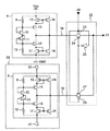
図1は、この発明の実施の形態1にかかる半導体集積回路装置の構成を示す。
この半導体集積回路装置は、通常動作モードとデータリテンションテストモードを有する。図1において、半導体集積回路装置は、電源電圧Vccを受けて1/2Vccの第1電圧(セルプレート電圧)を有する出力信号19を発生する第1電圧発生回路8と、第2電圧を有する出力信号32を発生する第2電圧発生回路29と、制御信号26に応じて出力信号19と出力信号32を切換えて、通常動作モードとデータリテンションテストモードで、夫々、出力信号19と出力信号32を出力信号33としてメモリセル50(図2)に印加するスイッチ回路22とを備える。
【0012】
図2は、半導体集積回路装置に設けられた複数のメモリセル50の1個の構成を示す。各メモリセル50は、1対のキャパシタ5を含むと共に、各キャパシタ5の両側に、夫々、電圧入力ノードNAと記憶ノードNBを有する。図1のスイッチ回路22の出力信号33は電圧入力ノードNAに印加される。ワード線1はメモリセル50を選択する一方、データがメモリセル50から1対のビット線2に出力される。メモリセル50は、更に、各々が薄膜トランジスタで形成される1対の負荷トランジスタ3と、各々が各負荷トランジスタ3と記憶ノードNBにおいて接続される1対の駆動トランジスタ4と、メモリセル50の記憶データをビット線2に伝達する1対のアクセストランジスタ7とを備える。
【0013】
図1に示すように、第1電圧発生回路8は、電源電圧Vccに接続された抵抗素子9と、抵抗素子9に直列接続されていると共にドレインとゲートが短絡したNチャネルMOSトランジスタ10と、NチャネルMOSトランジスタ10のソースにソースが直列接続されていると共にゲートとドレインが短絡したPチャネルMOSトランジスタ11と、一端がPチャネルMOSトランジスタ11のドレインに接続されていると共に他端が接地電圧GNDに接続された抵抗素子12と、夫々のソースが互いに接続されていると共に夫々のゲートが互いに接続されたPチャネルMOSトランジスタ13及び14とを備える。PチャネルMOSトランジスタ13において、ゲートとドレインが短絡している。
【0014】
第1電圧発生回路8は、更に、PチャネルMOSトランジスタ13のドレインにドレインが接続され、NチャネルMOSトランジスタ10のドレインにゲートが接続されていると共に出力信号19にソースが接続されたNチャネルMOSトランジスタ15と、出力信号19にソースが接続されていると共にPチャネルMOSトランジスタ11のドレインにゲートが接続されたPチャネルMOSトランジスタ16とを備える。
【0015】
第1電圧発生回路8は、更に、PチャネルMOSトランジスタ16のドレインにドレインとゲートが接続されていると共に接地電圧GNDにソースが接続されたNチャネルMOSトランジスタ17と、NチャネルMOSトランジスタ17のゲートとドレインの短絡ノードにゲートが接続され、出力信号19にドレインが接続されていると共に接地電圧GNDに接続したNチャネルMOSトランジスタ18とを備える。第1電圧発生回路8の出力信号19は1/2Vccの第1電圧を有する。
【0016】
上記構成の第1電圧発生回路8は以下のように動作する。NチャネルMOSトランジスタ15とPチャネルMOSトランジスタ16が、夫々、しきい電圧VthNとVthPを有する時、NチャネルMOSトランジスタ15のゲートは(1/2Vcc+VthN)の電圧レベルに設定される一方、PチャネルMOSトランジスタ16のゲートは(1/2Vcc−VthP)の電圧レベルに設定され、後述するように出力信号19の電圧レベルによりトランジスタ15と16の電流が変化する。
【0017】
トランジスタ15と16のその変化した電流により、トランジスタ15と16の夫々のドレインの電圧レベルが確定され、PチャネルMOSトランジスタ13及び14とNチャネルMOSトランジスタ17及び18によって形成されるカレントミラー回路で出力信号19の電圧レベルを安定させるように動作する。例えば、出力信号19の電圧レベルが1/2Vccより降下した場合、電流がNチャネルMOSトランジスタ15に流れるので、NチャネルMOSトランジスタ15のドレイン電圧、即ち、PチャネルMOSトランジスタ13及び14のゲート電圧が降下するから、電流が電源電圧Vcc側からPチャネルMOSトランジスタ14を介して出力信号19側に流れ込む結果、出力信号19の低下した電圧レベルが上昇する。
【0018】
逆に出力信号19の電圧レベルが1/2Vccより上昇した場合、電流がPチャネルMOSトランジスタ16に流れるので、PチャネルMOSトランジスタ16のドレイン電圧、即ち、NチャネルMOSトランジスタ17及び18のゲート電圧が上昇するから、電流が出力信号19側からNチャネルMOSトランジスタ18を介して電源電圧GND側に流れ込む結果、出力信号19の上昇した電圧レベルが降下する。第1電圧発生回路8の上記動作により、出力信号19の電圧レベルは1/2Vccに安定させられる。第1電圧発生回路8の出力信号19の第1電圧1/2Vccは、図2のメモリセル50の電圧入力ノードNAのセルプレート電圧として使用される。
【0019】
図1の半導体集積回路装置において、スイッチ回路22は、第1電圧発生回路8の出力信号19とスイッチ回路22の出力信号33に、夫々、ドレインとソースが接続されたNチャネルMOSトランジスタ23及びPチャネルMOSトランジスタ24と、第2電圧発生回路29の出力信号32とスイッチ回路33の出力信号33に、夫々、ドレインとソースが接続されたNチャネルMOSトランジスタ27及びPチャネルMOSトランジスタ28と、制御信号26を入力が受けるともにPチャネルMOSトランジスタ24のゲートとNチャネルMOSトランジスタ27のゲートを出力が制御するインバータ25とを備える。PチャネルMOSトランジスタ28のゲートは制御信号26で制御される。
【0020】
図1の半導体集積回路装置装置において、第2電圧発生回路29は、第1電圧発生回路8に、1/2Vccの電圧レベルを有する端子30と、−1/2Vccの電圧レベルを有する端子31とを付加した構成を有するので、第2電圧発生回路29の出力信号32の電圧レベルは接地電圧GNDに安定させられる。スイッチ回路22は、制御信号26に応じて、第1電圧発生回路8の出力信号19と第2電圧発生回路29の出力信号32を切換えて、出力信号33をメモリセル50の電圧入力ノードNAに印加する。
【0021】
例えば、半導体集積回路装置が通常動作モードである時、制御信号26がHレベルに設定されて、トランジスタ23と24がオンして、トランジスタ27と28がオフするので、1/2Vccの電圧レベルを有する出力信号19が出力信号33としてスイッチ回路22からメモリセル50の電圧入力モードNAに印加される。一方、半導体集積回路装置がデータリテンションテストモードである時、制御信号26がLレベルに設定されて、トランジスタ23と24がオフし、トランジスタ27と28がオンするので、接地電圧GNDを有する出力信号32が出力信号33としてスイッチ回路22からメモリセル50の電圧入力モードNAに印加される。
【0022】
メモリセル50の動作をスイッチ回路22の上記動作と関連させて図3のグラフを参照して説明する。時間を示す横軸と、電圧を示す縦軸を有する図3のグラフは、メモリセル50の電源電圧20とメモリセル50の記憶ノードNBのHレベル34の時間変化を、従来例のメモリセルの記憶ノードのHレベル21と対比して示す。間隔0〜t1では、メモリセル50の保証電圧範囲内の電源電圧20と記憶ノードNBのHレベル34は同一の高電圧V1である。
【0023】
間隔t1〜t2では、メモリセル50の電源電圧20が高電圧V1から低電圧V2まで大きく低下しているが、記憶ノードNBのHレベル34は、メモリセル50の電源電圧20に追従できずに高電圧V1よりも僅かに低い電圧に遷移している。時刻t3において、スイッチ回路22の制御信号26がHレベルからLレベルに設定される。メモリセル50の電源電圧20は時刻t5まで低電圧V2に維持されるが、記憶ノードNBのHレベル34は時刻t4で低電圧V2に遷移している。これに対し、従来例のメモリセルの記憶ノードのHレベル21は、時刻t5で低電圧V2に到達する。
【0024】
これは、この発明において、時刻t3において図1のスイッチ回路2の出力信号33が電圧1/2Vccから接地電圧GNDに変化するので、図2のメモリセル50において、キャパシタ5のカップリング効果により記憶ノードNBのHレベル34が迅速に低電圧V2に低下するためである。即ち、従来、電荷が負荷トランジスタ3を介して電源電圧Vcc側に少しずつ逃げていたのに対し、この発明では、電荷がキャパシタ5のカップリング効果によりメモリセル50の記憶ノードNBを迅速に遷移させることができる。
【0025】
この実施の形態では、スイッチ回路22が、通常動作モードでHレベルに設定されると共にデータリテンションテストモードでLレベルに設定される制御信号26に応じて、第1電圧発生回路8の出力信号19と第2電圧発生回路29の出力信号32を切換えて、通常動作モードとデータリテンションモードで、夫々、出力信号19と出力信号32を出力信号33としてメモリセル50の電圧入力ノードNAに印加するので、メモリセル50の記憶ノードNBを迅速に遷移させることができるから、データリテンションテストの所要時間を短縮することができる。
【0026】
実施の形態2.
図4は、この発明の実施の形態2にかかる半導体集積回路装置に用いられる第2電圧発生回路29の構成を示す。図4の第2電圧発生回路29は、接地電圧GNDを有する接地電源によって形成されている。この半導体集積回路装置の他の構成は図1の半導体集積回路装置と同様であるので、その説明を省略する。
【0027】
この実施の形態では、第2電圧発生回路29を接地電源によって形成しているので、データリテンションテストの所要時間を短縮することができるという実施の形態1の効果に加えて、第2電圧発生回路29が、故障無しに安全に動作することができると共に、回路のレイアウト面積を縮小することができる。
【0028】
実施の形態3.
図5は、この発明の実施の形態3にかかる半導体集積回路装置に用いられて、図1の制御信号26を発生する制御回路60の構成を示す。制御回路60は、データリテンションモードでの電源電圧を検知して、その電源電圧を示す電圧信号36を出力する電圧検知回路35と、データリテンションモードのスタンバイ状態を示すスタンバイ信号37を出力するスタンバイ信号発生回路45と、外部NC(no-connect)ピン(不図示)に接続されて、データリテンションテストモードを示すテストモード信号41をバッファー40を介して出力するパッド38とを備える。
【0029】
バッファー40は正論理インバータ51と負論理インバータ52を有する。外部NCピンのノードをLレベルに固定することができると共に、電源電圧Vccを受けるNチャネルMOSトランジスタ39が、パッド38とバッファー40の結合点に接続されている。制御回路60は、更に、電圧信号36、スタンバイ信号37とテストモード信号41を受けて、バッファー55を介して制御信号26を出力する3入力NANDゲート42を備える。バッファー55は負論理インバータ56と正論理インバータ57を有する。
【0030】
上記構成の制御回路60は以下のように動作する。外部NCピンからパッド38にHレベル信号が入力された時、Hレベルテストモード信号41がバッファー40を介して3入力NANDゲート42に入力される。又、3入力NANDゲート42は、Hレベルスタンバイ信号37を受ける。更に、3入力NANDゲート42が電圧検知回路35から受ける電圧信号36は、電源電圧が保証電圧範囲内である場合はLレベルに設定される一方、電源電圧がデータリテンションテストモード時の低電圧である場合はHレベルに切換え設定される。
【0031】
データリテンションテストモード時に、信号36、37と41は全てHレベルであるので、3入力NANDゲート42はバッファー55を介してLレベル制御信号26を出力する。Lレベル制御信号26を受けたスイッチ回路22は、データリテンションテストモードに対応する出力信号32を出力信号33としてメモリセル50の電圧入力ノードNAに印加するので、メモリセル50の記憶ノードNBを迅速に遷移させることができるから、データリテンションテストの所要時間を短縮することができる。逆に、信号36、37と41がすべてHレベルである時を除いて、制御回路60はHレベル制御信号26を出力するので、Hレベル制御信号26を受けたスイッチ回路22は、通常動作モードに対応する出力信号19を出力信号33としてメモリセル50の電圧入力ノードNAに印加する。
【0032】
この実施の形態では、3入力NANDゲート42が、少なくとも電圧信号36とスタンバイ信号37、又は、電圧信号36、スタンバイ信号37とテストモード信号41を論理演算して、制御信号26を出力するように構成しているので、スイッチ回路22は、制御信号26に基づいて出力信号19と出力信号32を確実に切換えるから、半導体集積回路装置をユーザが使用中の誤作動を未然に回避することができる。
【0033】
なお、実施の形態1〜3においては、SRAM型メモリセルにキャパシタを用いた場合について示したが、DRAMのキャパシタに用いても良い。
【0034】
【発明の効果】
以上のように、請求項1の発明によれば、半導体集積回路装置が、各々がキャパシタを含むと共に各々が前記キャパシタの両側に、夫々、電圧入力ノードと記憶ノードを有する複数のメモリセルと、第1電圧を発生する第1電圧発生回路と、前記第1電圧より低い第2電圧を発生する第2電圧発生回路と、前記第1電圧と前記第2電圧を受けると共に、通常動作モードで前記第1電圧を前記電圧入力ノードに出力する一方、データリテンションテストモードで前記第2電圧を前記電圧入力ノードに出力するように、制御信号に応じて前記第1電圧と前記第2電圧を切換えるスイッチ回路とを備えるので、スイッチ回路が、制御信号に応じて、第1電圧と第2電圧を切換えて、通常動作モードとデータリテンションモードで、夫々、第1電圧と第2電圧を出力信号としてメモリセルの電圧入力ノードに印加するので、メモリセルの記憶ノードを迅速に遷移させることができるから、データリテンションテストの所要時間を短縮することができる。
【図面の簡単な説明】
【図1】この発明の実施の形態1にかかる半導体集積回路装置の構成を示す回路図である。
【図2】図1の半導体集積回路装置に用いられる複数のメモリセルの1個の構成を示す回路図である。
【図3】図2のメモリセルの動作を示すグラフである。
【図4】この発明の実施の形態2にかかる半導体集積回路装置に用いられる第2電圧発生回路の構成を示す回路図である。
【図5】この発明の実施の形態3にかかる半導体集積回路装置に用いられる制御回路の構成を示す回路図である。
【符号の説明】
1 ワード線、 2 ビット線、 5 キャパシタ、 8 第1電圧発生回路、 19 出力信号、 22 スイッチ回路、 26 制御信号、 29 第2電圧発生回路、 32 出力信号、 35 電圧検知回路、 38 パッド、 42 3入力NANDゲート、 45 スタンバイ信号発生回路、 50 メモリセル、 60 制御回路。[0001]
TECHNICAL FIELD OF THE INVENTION
The present invention generally relates to a semiconductor integrated circuit device including a plurality of memory cells each including a capacitor and each having a voltage input node and a storage node on both sides of the capacitor. The present invention relates to a semiconductor integrated circuit device that can reduce the time required for a data retention test by utilizing the device.
[0002]
[Prior art]
When writing or reading data to or from a plurality of memory cells each including a capacitor, the power supply voltage is within the guaranteed voltage range of 2.7 V to 3.6 V when the power supply voltage is 3 V, and 1.6 V when the power supply voltage is 1.8 V. Within the guaranteed voltage range of up to 2.3 V, the word line of the selected memory cell is set from L level to H level, and the access transistor is turned on.
At the time of writing, desired L level or H level data on the bit line to be written is transmitted to the storage node via the access transistor. On the other hand, at the time of reading, desired L-level or H-level data stored in the storage node of the memory cell is transmitted to the bit line via the access transistor.
[0003]
The memory cell also needs to have a property of retaining data even outside the guaranteed voltage range, that is, a data retention property. When the memory cell has data retention characteristics, for example, even if the power supply voltage of 3 V drops to 2 V outside the guaranteed voltage range of 2.7 V to 3.6 V, data stored in the memory cell may be destroyed. Is kept without. In this case, the data written within the guaranteed voltage range of 2.7 V to 3.6 V is maintained at 2 V outside the guaranteed voltage range, and when the data is read within the guaranteed voltage range, the data is read. Can be put out.
[0004]
In order to confirm whether or not the memory cell has data retention characteristics, a data retention test is performed in a pre-shipment inspection of a semiconductor product using the memory cell. In order to reduce the production cost of semiconductor products, it is desirable to reduce the time required for a data retention test.
[0005]
However, in the conventional memory cell, even if the power supply voltage falls outside the guaranteed voltage range, the H level of the storage node does not immediately decrease. This is because the charge at the storage node escapes only to the power supply side of the memory cell, and the load transistor leading to the power supply has a very high resistance value. As a result, there is a problem that the time required for a data retention test in a pre-shipment inspection of a conventional semiconductor product using a memory cell becomes long.
[0006]
Therefore, in order to reduce the waiting time of the data pretension test, for example, Patent Literature 1 proposes to add a parasitic capacitance between a plate serving as a reference level of a capacitor and a power supply. However, Patent Document 1 differs from the present invention in that a parasitic capacitance is added.
[0007]
[Patent Document 1]
JP-A-5-101649 (paragraph 16, FIGS. 1 and 2)
[0008]
[Problems to be solved by the invention]
SUMMARY OF THE INVENTION The present invention has been made to solve the above-described problems of the prior art, and the H level of a storage node is rapidly lowered by utilizing the coupling effect of a capacitor of a memory cell, thereby enabling a data retention test to be performed. It is an object of the present invention to provide a semiconductor integrated circuit device capable of reducing time.
[0009]
[Means for Solving the Problems]
2. The semiconductor integrated circuit device according to claim 1, wherein each of the plurality of memory cells includes a capacitor and has a voltage input node and a storage node on both sides of the capacitor, respectively, and a first voltage for generating a first voltage. A generating circuit, a second voltage generating circuit for generating a second voltage lower than the first voltage, receiving the first voltage and the second voltage, and applying the first voltage to the voltage input node in a normal operation mode And a switch circuit for switching between the first voltage and the second voltage according to a control signal so as to output the second voltage to the voltage input node in the data retention test mode while outputting the data.
[0010]
BEST MODE FOR CARRYING OUT THE INVENTION
Hereinafter, embodiments of the present invention will be described with reference to the drawings.
[0011]
Embodiment 1 FIG.
FIG. 1 shows a configuration of a semiconductor integrated circuit device according to a first embodiment of the present invention.
This semiconductor integrated circuit device has a normal operation mode and a data retention test mode. 1, a semiconductor integrated circuit device receives a power supply voltage Vcc, generates an output signal 19 having a first voltage (cell plate voltage) of 1/2 Vcc, and an output having a second voltage. The output signal 19 and the output signal 32 are switched in the normal operation mode and the data retention test mode by switching between the output signal 19 and the output signal 32 according to the control signal 26 and the second voltage generation circuit 29 for generating the signal 32. And a switch circuit 22 for applying an output signal 33 to the memory cell 50 (FIG. 2).
[0012]
FIG. 2 shows one configuration of a plurality of memory cells 50 provided in the semiconductor integrated circuit device. Each memory cell 50 includes a pair of capacitors 5, and has a voltage input node NA and a storage node NB on both sides of each capacitor 5, respectively. The output signal 33 of the switch circuit 22 of FIG. 1 is applied to the voltage input node NA. Word line 1 selects memory cell 50, while data is output from memory cell 50 to a pair of bit lines 2. The memory cell 50 further includes a pair of load transistors 3 each formed of a thin film transistor, a pair of drive transistors 4 each connected to each load transistor 3 at a storage node NB, and data stored in the memory cell 50. Is transmitted to the bit line 2.
[0013]
As shown in FIG. 1, the first voltage generating circuit 8 includes a resistor 9 connected to the power supply voltage Vcc, an N-channel MOS transistor 10 connected in series to the resistor 9 and having a drain and a gate short-circuited. A P-channel MOS transistor 11 whose source is connected in series to the source of N-channel MOS transistor 10 and whose gate and drain are short-circuited, one end of which is connected to the drain of P-channel MOS transistor 11 and the other end of which is ground voltage GND. , And P-channel MOS transistors 13 and 14 whose sources are connected to each other and whose gates are connected to each other. In the P-channel MOS transistor 13, the gate and the drain are short-circuited.
[0014]
The first voltage generating circuit 8 further includes an N-channel MOS transistor having a drain connected to the drain of the P-channel MOS transistor 13, a gate connected to the drain of the N-channel MOS transistor 10, and a source connected to the output signal 19. A transistor 15 includes a P-channel MOS transistor 16 whose source is connected to the output signal 19 and whose gate is connected to the drain of the P-channel MOS transistor 11.
[0015]
The first voltage generating circuit 8 further includes an N-channel MOS transistor 17 having a drain and a gate connected to the drain of the P-channel MOS transistor 16 and a source connected to the ground voltage GND, and a gate of the N-channel MOS transistor 17. And an N-channel MOS transistor 18 having a gate connected to the short-circuit node of the drain, a drain connected to the output signal 19, and connected to the ground voltage GND. Output signal 19 of first voltage generating circuit 8 has a first voltage of 1/2 Vcc.
[0016]
The first voltage generating circuit 8 having the above configuration operates as follows. When N-channel MOS transistor 15 and P-channel MOS transistor 16 have threshold voltages VthN and VthP, respectively, the gate of N-channel MOS transistor 15 is set to the voltage level of (1 / Vcc + VthN), while the P-channel MOS transistor The gate of the transistor 16 is set to a voltage level of (1/2 Vcc-VthP), and the current of the transistors 15 and 16 changes according to the voltage level of the output signal 19 as described later.
[0017]
The changed currents of the transistors 15 and 16 determine the voltage levels of the drains of the transistors 15 and 16, respectively, and output the current in the current mirror circuit formed by the P-channel MOS transistors 13 and 14 and the N-channel MOS transistors 17 and 18. It operates to stabilize the voltage level of the signal 19. For example, when the voltage level of the output signal 19 drops below V Vcc, a current flows through the N-channel MOS transistor 15, so that the drain voltage of the N-channel MOS transistor 15, ie, the gate voltages of the P-channel MOS transistors 13 and 14, Since the current drops, the current flows from the power supply voltage Vcc side to the output signal 19 side via the P-channel MOS transistor 14, so that the lowered voltage level of the output signal 19 increases.
[0018]
Conversely, if the voltage level of output signal 19 rises above 1/2 Vcc, a current flows through P-channel MOS transistor 16, so that the drain voltage of P-channel MOS transistor 16, that is, the gate voltages of N-channel MOS transistors 17 and 18 are increased. Since the current rises, the current flows from the output signal 19 side to the power supply voltage GND side via the N-channel MOS transistor 18, so that the increased voltage level of the output signal 19 falls. By the above operation of the first voltage generation circuit 8, the voltage level of the output signal 19 is stabilized at 1/2 Vcc. The first voltage 1/2 Vcc of the output signal 19 of the first voltage generation circuit 8 is used as the cell plate voltage of the voltage input node NA of the memory cell 50 in FIG.
[0019]
In the semiconductor integrated circuit device of FIG. 1, the switch circuit 22 includes an N-channel MOS transistor 23 having a drain and a source connected to an output signal 19 of the first voltage generation circuit 8 and an output signal 33 of the switch circuit 22, respectively. A channel MOS transistor 24, an output signal 32 of a second voltage generation circuit 29, and an output signal 33 of a switch circuit 33 are respectively connected to an N-channel MOS transistor 27 and a P-channel MOS transistor 28 whose drain and source are connected, and a control signal. An inverter 25 receives an input 26 and controls the gate of a P-channel MOS transistor 24 and the gate of an N-channel MOS transistor 27. The gate of P channel MOS transistor 28 is controlled by control signal 26.
[0020]
In the semiconductor integrated circuit device shown in FIG. 1, the second voltage generation circuit 29 includes a first voltage generation circuit 8 having a terminal 30 having a voltage level of 1/2 Vcc and a terminal 31 having a voltage level of -1/2 Vcc. , The voltage level of the output signal 32 of the second voltage generation circuit 29 is stabilized at the ground voltage GND. The switch circuit 22 switches the output signal 19 of the first voltage generation circuit 8 and the output signal 32 of the second voltage generation circuit 29 according to the control signal 26, and outputs the output signal 33 to the voltage input node NA of the memory cell 50. Apply.
[0021]
For example, when the semiconductor integrated circuit device is in the normal operation mode, the control signal 26 is set to the H level, the transistors 23 and 24 are turned on, and the transistors 27 and 28 are turned off. The output signal 19 is applied as an output signal 33 from the switch circuit 22 to the voltage input mode NA of the memory cell 50. On the other hand, when the semiconductor integrated circuit device is in the data retention test mode, control signal 26 is set to L level, transistors 23 and 24 are turned off, and transistors 27 and 28 are turned on, so that output signal having ground voltage GND is output. 32 is applied as an output signal 33 from the switch circuit 22 to the voltage input mode NA of the memory cell 50.
[0022]
The operation of the memory cell 50 will be described with reference to the graph of FIG. The graph of FIG. 3 having a horizontal axis indicating time and a vertical axis indicating voltage shows the time change of the power supply voltage 20 of the memory cell 50 and the H level 34 of the storage node NB of the memory cell 50 with respect to the conventional memory cell. It is shown in comparison with the H level 21 of the storage node. In the interval 0 to t1, the power supply voltage 20 within the guaranteed voltage range of the memory cell 50 and the H level 34 of the storage node NB are the same high voltage V1.
[0023]
In the interval t1 to t2, the power supply voltage 20 of the memory cell 50 is greatly reduced from the high voltage V1 to the low voltage V2, but the H level 34 of the storage node NB cannot follow the power supply voltage 20 of the memory cell 50 The voltage transits to a voltage slightly lower than the high voltage V1. At time t3, the control signal 26 of the switch circuit 22 is set from H level to L level. The power supply voltage 20 of the memory cell 50 is maintained at the low voltage V2 until time t5, but the H level 34 of the storage node NB transitions to the low voltage V2 at time t4. On the other hand, the H level 21 of the storage node of the conventional memory cell reaches the low voltage V2 at time t5.
[0024]
This is because, in the present invention, at time t3, output signal 33 of switch circuit 2 in FIG. 1 changes from voltage 1/2 Vcc to ground voltage GND, so that memory cell 50 in FIG. This is because the H level 34 of the node NB quickly drops to the low voltage V2. That is, in contrast to the conventional structure in which electric charge gradually escapes to the power supply voltage Vcc side via the load transistor 3, in the present invention, the electric charge quickly changes the storage node NB of the memory cell 50 due to the coupling effect of the capacitor 5. Can be done.
[0025]
In this embodiment, switch circuit 22 sets output signal 19 of first voltage generation circuit 8 in response to control signal 26 which is set to H level in the normal operation mode and set to L level in data retention test mode. And the output signal 32 of the second voltage generating circuit 29 are switched to apply the output signal 19 and the output signal 32 to the voltage input node NA of the memory cell 50 as the output signal 33 in the normal operation mode and the data retention mode, respectively. Since the transition of the storage node NB of the memory cell 50 can be performed quickly, the time required for the data retention test can be reduced.
[0026]
Embodiment 2 FIG.
FIG. 4 shows a configuration of the second voltage generation circuit 29 used in the semiconductor integrated circuit device according to the second embodiment of the present invention. 4 is formed by a ground power supply having a ground voltage GND. The other configuration of the semiconductor integrated circuit device is the same as that of the semiconductor integrated circuit device of FIG.
[0027]
In this embodiment, since the second voltage generation circuit 29 is formed by a ground power supply, the time required for the data retention test can be reduced, and in addition to the effect of the first embodiment, the second voltage generation circuit 29 29 can operate safely without failure and can reduce the circuit layout area.
[0028]
Embodiment 3 FIG.
FIG. 5 shows a configuration of a control circuit 60 for generating the control signal 26 of FIG. 1 used in the semiconductor integrated circuit device according to the third embodiment of the present invention. The control circuit 60 detects a power supply voltage in the data retention mode, and outputs a voltage signal 36 indicating the power supply voltage, and a standby signal 37 outputs a standby signal 37 indicating a standby state in the data retention mode. A generating circuit 45 and a pad 38 connected to an external NC (no-connect) pin (not shown) and outputting a test mode signal 41 indicating a data retention test mode via a buffer 40 are provided.
[0029]
The buffer 40 has a positive logic inverter 51 and a negative logic inverter 52. The node of the external NC pin can be fixed at L level, and an N-channel MOS transistor 39 receiving power supply voltage Vcc is connected to a connection point between pad 38 and buffer 40. The control circuit 60 further includes a three-input NAND gate 42 that receives the voltage signal 36, the standby signal 37, and the test mode signal 41 and outputs the control signal 26 via the buffer 55. The buffer 55 has a negative logic inverter 56 and a positive logic inverter 57.
[0030]
The control circuit 60 having the above configuration operates as follows. When an H level signal is input to the pad 38 from the external NC pin, an H level test mode signal 41 is input to the three-input NAND gate 42 via the buffer 40. Further, three-input NAND gate 42 receives H-level standby signal 37. Further, the voltage signal 36 received by the three-input NAND gate 42 from the voltage detection circuit 35 is set to L level when the power supply voltage is within the guaranteed voltage range, while the power supply voltage is set to a low voltage in the data retention test mode. In some cases, the level is switched to H level.
[0031]
In the data retention test mode, signals 36, 37 and 41 are all at H level, so 3-input NAND gate 42 outputs L level control signal 26 via buffer 55. The switch circuit 22 that has received the L level control signal 26 applies the output signal 32 corresponding to the data retention test mode to the voltage input node NA of the memory cell 50 as the output signal 33, so that the storage node NB of the memory cell 50 is quickly connected. , The time required for the data retention test can be reduced. Conversely, the control circuit 60 outputs the H level control signal 26 except when the signals 36, 37 and 41 are all at the H level, so that the switch circuit 22 receiving the H level control signal 26 operates in the normal operation mode. Is applied to the voltage input node NA of the memory cell 50 as the output signal 33.
[0032]
In this embodiment, the three-input NAND gate 42 performs a logical operation on at least the voltage signal 36 and the standby signal 37, or the voltage signal 36, the standby signal 37, and the test mode signal 41, and outputs the control signal 26. With this configuration, the switch circuit 22 reliably switches between the output signal 19 and the output signal 32 based on the control signal 26, so that a malfunction during use of the semiconductor integrated circuit device by a user can be avoided. .
[0033]
In the first to third embodiments, the case where the capacitor is used for the SRAM type memory cell has been described, but the capacitor may be used for the DRAM.
[0034]
【The invention's effect】
As described above, according to the first aspect of the present invention, a semiconductor integrated circuit device includes a plurality of memory cells each including a capacitor and each having a voltage input node and a storage node on both sides of the capacitor, respectively. A first voltage generating circuit for generating a first voltage, a second voltage generating circuit for generating a second voltage lower than the first voltage, receiving the first voltage and the second voltage, and in the normal operation mode, A switch for switching between the first voltage and the second voltage in response to a control signal so as to output a first voltage to the voltage input node and output the second voltage to the voltage input node in a data retention test mode. Circuit, the switch circuit switches between the first voltage and the second voltage according to the control signal, and switches the first voltage and the second voltage in the normal operation mode and the data retention mode, respectively. Since applied to the voltage input node of the memory cell 2 voltage as the output signal, because it is possible to quickly transition the storage node of the memory cell, it is possible to shorten the time required for data retention test.
[Brief description of the drawings]
FIG. 1 is a circuit diagram showing a configuration of a semiconductor integrated circuit device according to a first embodiment of the present invention;
FIG. 2 is a circuit diagram showing one configuration of a plurality of memory cells used in the semiconductor integrated circuit device of FIG.
FIG. 3 is a graph showing an operation of the memory cell of FIG. 2;
FIG. 4 is a circuit diagram showing a configuration of a second voltage generation circuit used in a semiconductor integrated circuit device according to a second embodiment of the present invention;
FIG. 5 is a circuit diagram showing a configuration of a control circuit used in a semiconductor integrated circuit device according to a third embodiment of the present invention;
[Explanation of symbols]
1 word line, 2 bit line, 5 capacitor, 8 first voltage generation circuit, 19 output signal, 22 switch circuit, 26 control signal, 29 second voltage generation circuit, 32 output signal, 35 voltage detection circuit, 38 pad, 42 3 input NAND gate, 45 standby signal generation circuit, 50 memory cell, 60 control circuit.