JP2004194355A - Automatic gain control circuit - Google Patents

Automatic gain control circuit Download PDF

Info

Publication number
JP2004194355A
JP2004194355A JP2004046220A JP2004046220A JP2004194355A JP 2004194355 A JP2004194355 A JP 2004194355A JP 2004046220 A JP2004046220 A JP 2004046220A JP 2004046220 A JP2004046220 A JP 2004046220A JP 2004194355 A JP2004194355 A JP 2004194355A
Authority
JP
Japan
Prior art keywords
signal
attenuation
agc
axis signal
axis
Prior art date
Legal status (The legal status is an assumption and is not a legal conclusion. Google has not performed a legal analysis and makes no representation as to the accuracy of the status listed.)
Granted
Application number
JP2004046220A
Other languages
Japanese (ja)
Other versions
JP4123166B2 (en
Inventor
Shigeki Yamauchi
茂樹 山内
Current Assignee (The listed assignees may be inaccurate. Google has not performed a legal analysis and makes no representation or warranty as to the accuracy of the list.)
Oki Electric Industry Co Ltd
Original Assignee
Oki Electric Industry Co Ltd
Priority date (The priority date is an assumption and is not a legal conclusion. Google has not performed a legal analysis and makes no representation as to the accuracy of the date listed.)
Filing date
Publication date
Application filed by Oki Electric Industry Co Ltd filed Critical Oki Electric Industry Co Ltd
Priority to JP2004046220A priority Critical patent/JP4123166B2/en
Publication of JP2004194355A publication Critical patent/JP2004194355A/en
Application granted granted Critical
Publication of JP4123166B2 publication Critical patent/JP4123166B2/en
Anticipated expiration legal-status Critical
Expired - Fee Related legal-status Critical Current

Links

Images

Abstract

<P>PROBLEM TO BE SOLVED: To provide an automatic gain control (AGC) circuit in which non-linear distortion is prevented from being incurred by an adjacent channel signal. <P>SOLUTION: An I-axis signal and a Q-axis signal demodulated by a demodulator 16 are inputted through a variable resistor 40, a DC amplifier 18 and an analog filter 20 to a delay circuit 44 and an analog filter 43 as a signal 130, the signal 130 becomes a signal 132 by adjusting its phase and amplified by the delay circuit 44 and a variable gain amplifier 46, only a desired channel signal component is extracted by the analog filter 42 to be the signal 134, and the signals are respectively inputted to a differential amplifier 48. In the differential amplifier 48, an adjacent signal component 136 is generated from the signal 132 and the signal 134. In a comparator 50, a peak value of the signal component 136 is detected and compared with a threshold 142, an SW changeover signal 138 instructing an attenuation quantity is generated and supplied to the variable resistor 40. In an EN signal generator 52, an EN signal indicating a switch timing of the attenuation quantity is generated and outputted to the variable resistor 40. <P>COPYRIGHT: (C)2004,JPO&NCIPI

Description

本発明は、CDMA(Code Division Multiple Access)無線通信装置の受信部で使用される自動利得制御回路(以下、AGC回路という)に関する。   The present invention relates to an automatic gain control circuit (hereinafter, referred to as an AGC circuit) used in a receiving section of a CDMA (Code Division Multiple Access) wireless communication device.

CDMA無線通信装置の受信部は、たとえば、受信ミキサ、SAWフィルタ、AGC増幅器、直交変調信号を復調する復調器、アナログ・デジタル変換器、AGC機能回路等を含み、アンテナにより受信した高周波信号を受信ミキサによりIF(中間周波数)信号に変換し、SAWフィルタにより希望チャネル信号を選択してAGC増幅器によりレベル調整し、レベル調整した信号を復号器により復調してI軸信号およびQ軸信号を生成し、生成したI軸信号およびQ軸信号をアナログ・デジタル変換回路によりデジタル化するものであった。そして、AGC機能回路により、デジタル化されたI軸信号およびQ軸信号のパワーを算出して予め定められた閾値と比較し、閾値との差に応じてAGC増幅器の利得を制御することによりアナログ・デジタル変換器の入力レベルを一定にしていた。
特開平11−261433号公報 特開平11−195941号公報
The receiving unit of the CDMA wireless communication device includes, for example, a reception mixer, a SAW filter, an AGC amplifier, a demodulator for demodulating a quadrature modulated signal, an analog-to-digital converter, an AGC function circuit, and the like, and receives a high-frequency signal received by an antenna. The signal is converted to an IF (intermediate frequency) signal by a mixer, a desired channel signal is selected by a SAW filter, the level is adjusted by an AGC amplifier, and the level-adjusted signal is demodulated by a decoder to generate an I-axis signal and a Q-axis signal. , The generated I-axis signal and Q-axis signal are digitized by an analog / digital conversion circuit. The AGC function circuit calculates the power of the digitized I-axis signal and Q-axis signal, compares the calculated power with a predetermined threshold value, and controls the gain of the AGC amplifier according to the difference from the threshold value. -The input level of the digital converter was kept constant.
JP-A-11-261433 JP-A-11-195941

しかしながら、上記のAGC機能回路では、デジタル化されたI軸信号およびQ軸信号を使用してAGC増幅器の利得を制御するAGC電圧を生成していたため、AGC機能をデジタル処理信号回路で実現する必要があった。このため、装置におけるデジタル信号処理回路の規模が大きくなるという問題があった。   However, in the above-mentioned AGC function circuit, since the AGC voltage for controlling the gain of the AGC amplifier is generated using the digitized I-axis signal and Q-axis signal, it is necessary to realize the AGC function by a digital processing signal circuit. was there. For this reason, there is a problem that the scale of the digital signal processing circuit in the device becomes large.

本発明は、このような従来の技術の問題点を解決するもので、AGC機能をアナログ回路で構成したAGC回路を提供することを目的とする。   An object of the present invention is to solve such a problem of the conventional technology, and to provide an AGC circuit in which an AGC function is configured by an analog circuit.

本発明による自動利得制御回路は上記の問題を解決するために、直交変調された受信信号を復調してI軸信号およびQ軸信号を出力する復調器と、切替信号に従って減衰量を第1の減衰量または第1の減衰量より大きい第2の減衰量に切り替えて復調器から出力されるI軸信号およびQ軸信号に減衰を与える可変抵抗器と、可変抵抗器から出力されるI軸信号およびQ軸信号の希望チャネル信号成分を通過させる第1のアナログフィルタと、第1のアナログフィルタから出力されるI軸信号およびQ軸信号をデータに変換するアナログ・デジタル変換器とを含む無線装置受信部の自動利得制御回路において、第1のアナログフィルタから出力されるI軸信号およびQ軸信号の希望チャネル信号成分を通過させる第2のアナログフィルタと、第2のアナログフィルタから出力されるI軸信号およびQ軸信号に所定の遅延を与える遅延手段と、遅延手段を通過した信号のレベルを調整する可変利得増幅手段と、可変利得増幅手段から出力される信号から、第2のアナログフィルタから出力される信号を減算して隣接チャネル信号成分を算出し、隣接チャネル信号成分が閾値を超えた時可変抵抗器の減衰量を第2の減衰量に切り替え、隣接チャネル信号成分が閾値より低下した時可変抵抗器の減衰量を第1の減衰量に切り替える切替信号を生成する比較手段とを含むことを特徴とする。   In order to solve the above problem, an automatic gain control circuit according to the present invention demodulates a quadrature-modulated received signal to output an I-axis signal and a Q-axis signal, and reduces an amount of attenuation according to a switching signal by a first amount. A variable resistor that switches to an attenuation amount or a second attenuation amount larger than the first attenuation amount to attenuate the I-axis signal and the Q-axis signal output from the demodulator, and an I-axis signal output from the variable resistor And a first analog filter for passing desired channel signal components of the Q and Q axis signals, and an analog / digital converter for converting the I axis signal and the Q axis signal output from the first analog filter into data. An automatic gain control circuit of the receiving unit, wherein a second analog filter that passes desired channel signal components of the I-axis signal and the Q-axis signal output from the first analog filter; Delay means for giving a predetermined delay to the I-axis signal and the Q-axis signal output from the analog filter, a variable gain amplifying means for adjusting the level of the signal passing through the delay means, and a signal output from the variable gain amplifying means , The adjacent channel signal component is calculated by subtracting the signal output from the second analog filter, and when the adjacent channel signal component exceeds the threshold, the attenuation of the variable resistor is switched to the second attenuation, And a comparator for generating a switching signal for switching the attenuation of the variable resistor to the first attenuation when the channel signal component falls below the threshold.

本発明によれば、AGC回路をアナログ回路により構成しているので、装置におけるデジタル信号処理回路の規模を縮小することができる。また、AGC回路により時定数を含まない可変アッテネータを制御することによりレベル制御を行っているので、隣接チャネル成分のレベルが急激に変化した場合でも迅速に対応できる。   According to the present invention, since the AGC circuit is configured by an analog circuit, the scale of the digital signal processing circuit in the device can be reduced. Further, since the level control is performed by controlling the variable attenuator that does not include the time constant by the AGC circuit, it is possible to quickly cope with a sudden change in the level of the adjacent channel component.

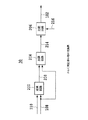
次に添付図面を参照して本発明によるAGC回路の実施例を詳細に説明する。図1は、本発明によるAGC回路の第1の実施例を示すブロックである。図1において、受信ミキサ10、SAWフィルタ12、復調器16、可変抵抗器40、直流増幅器18、アナログフィルタ20、およびアナログ・デジタル変換器(ADC)22は受信部の一部を構成する。また、アナログフィルタ42、遅延回路44、可変利得増幅器46、差動増幅器48、比較器50およびEN信号発生器52はすべてアナログ回路であり、AGC回路を構成する。なお、AGC回路は、I軸信号およびQ軸信号を別々に平行して処理するものとする。また、接続線に付された参照符号はその接続線に現れる信号を示す。   Next, an embodiment of the AGC circuit according to the present invention will be described in detail with reference to the accompanying drawings. FIG. 1 is a block diagram showing a first embodiment of the AGC circuit according to the present invention. In FIG. 1, a reception mixer 10, a SAW filter 12, a demodulator 16, a variable resistor 40, a DC amplifier 18, an analog filter 20, and an analog-to-digital converter (ADC) 22 constitute a part of a reception unit. The analog filter 42, the delay circuit 44, the variable gain amplifier 46, the differential amplifier 48, the comparator 50, and the EN signal generator 52 are all analog circuits and constitute an AGC circuit. The AGC circuit processes the I-axis signal and the Q-axis signal separately and in parallel. Further, reference symbols attached to connection lines indicate signals appearing on the connection lines.

受信ミキサ10は、高周波信号100をIF信号に変換する周波数変換器であり、ダブルスーパーヘテロダイン方式の場合は2番目の受信ミキサに該当する。受信ミキサ10に接続されたSAWフィルタ12は、たとえば、通過帯域が5MHzのバンドパスフィルタであり、受信ミキサ10により周波数変換された信号から所望のチャネル信号(希望チャネル信号)を選択し、他のチャネル信号(隣接チャネル信号)を減衰させる表面弾性波フィルタである。SAWフィルタ12に接続された復調器16は、直交変調された信号を復調する復調器であり、入力信号を復調してI軸信号およびQ軸信号を出力するものである。   The reception mixer 10 is a frequency converter that converts the high-frequency signal 100 into an IF signal, and corresponds to a second reception mixer in the case of the double superheterodyne system. The SAW filter 12 connected to the reception mixer 10 is, for example, a band-pass filter having a pass band of 5 MHz. The SAW filter 12 selects a desired channel signal (desired channel signal) from a signal whose frequency has been converted by the reception mixer 10. This is a surface acoustic wave filter that attenuates a channel signal (adjacent channel signal). The demodulator 16 connected to the SAW filter 12 is a demodulator that demodulates a quadrature-modulated signal, and outputs an I-axis signal and a Q-axis signal by demodulating an input signal.

復調器16に接続された可変抵抗器40は、復調器16から入力される信号に減衰を与える可変アッテネータを有し、EN信号発生器52からEN信号144が与えられたとき、比較器50から供給されるSW切替信号138に従って可変アッテネータの減衰量を変更するものであり、本実施例では、減衰量を第1の減衰量および第2の減衰量のいずれかに設定することができる。ただし、第2の減衰量は第1の減衰量より大きいものとする。   The variable resistor 40 connected to the demodulator 16 has a variable attenuator that attenuates the signal input from the demodulator 16, and when an EN signal 144 is given from the EN signal generator 52, the variable resistor 40 The attenuation of the variable attenuator is changed in accordance with the supplied SW switching signal 138. In this embodiment, the attenuation can be set to one of the first attenuation and the second attenuation. However, the second attenuation is larger than the first attenuation.

可変抵抗器40に接続された直流増幅器18は、復調器16から出力されるI軸信号およびQ軸信号を増幅する増幅回路であり、直流増幅器18に接続されたアナログフィルタ20は、直流増幅器18から出力される信号から隣接チャネル信号のI軸信号およびQ軸信号(隣接チャネル信号成分)を除去して希望チャネル信号のI軸信号およびQ軸信号(希望チャネル信号成分)を出力するローパスフィルタである。アナログフィルタ20に接続されたアナログ・デジタル変換器22は、アナログフィルタ20から出力されるI軸信号およびQ軸信号をアナログ信号からデジタル信号に変換し、I軸信号の振幅値を示すデータIおよびQ軸信号の振幅値を示すデータQからなるデータ106を出力するものである。   The DC amplifier 18 connected to the variable resistor 40 is an amplifier circuit for amplifying the I-axis signal and the Q-axis signal output from the demodulator 16, and the analog filter 20 connected to the DC amplifier 18 A low-pass filter that removes the I-axis signal and the Q-axis signal (adjacent channel signal component) of the adjacent channel signal from the signal output from and outputs the I-axis signal and the Q-axis signal (desired channel signal component) of the desired channel signal is there. An analog / digital converter 22 connected to the analog filter 20 converts the I-axis signal and the Q-axis signal output from the analog filter 20 from an analog signal to a digital signal, and outputs data I and I indicating the amplitude value of the I-axis signal. It outputs data 106 including data Q indicating the amplitude value of the Q-axis signal.

アナログフィルタ20に接続されたアナログフィルタ42は、本実施例では、アナログフィルタ20と同一の帯域特性を有するローパスフィルタである。したがって、アナログフィルタ20から出力される信号130に残っている隣接チャネル信号成分はアナログフィルタ42により除去され、アナログフィルタ42から出力される信号132は、希望チャネル信号成分のみとなる。   In the present embodiment, the analog filter 42 connected to the analog filter 20 is a low-pass filter having the same band characteristics as the analog filter 20. Therefore, the adjacent channel signal component remaining in the signal 130 output from the analog filter 20 is removed by the analog filter 42, and the signal 132 output from the analog filter 42 becomes only the desired channel signal component.

アナログフィルタ20に接続された遅延回路44は、入力信号130に所定の遅延を与えるものであり、遅延回路44に接続されている可変利得増幅器46は、信号レベルを調整する利得可変手段を備えている。本実施例では、可変利得増幅器46から出力される信号134に含まれる希望チャネル信号成分の振幅および位相がアナログフィルタ42から出力される信号132と同じになるように、遅延回路44の遅延時間および可変利得増幅器46の利得を調整している。   The delay circuit 44 connected to the analog filter 20 applies a predetermined delay to the input signal 130, and the variable gain amplifier 46 connected to the delay circuit 44 includes a variable gain means for adjusting a signal level. I have. In the present embodiment, the delay time of the delay circuit 44 and the delay time of the delay circuit 44 are set so that the amplitude and the phase of the desired channel signal component included in the signal 134 output from the variable gain amplifier 46 become the same as the signal 132 output from the analog filter 42. The gain of the variable gain amplifier 46 is adjusted.

アナログフィルタ42および可変利得増幅器46に接続された差動増幅器48は、可変利得増幅器46から出力される信号134からアナログフィルタ42から出力される信号132を減算し、その差を信号136として出力するものである。前述のように、隣接チャネル信号成分が大きい場合には、アナログフィルタ20から出力される信号130に隣接チャネル信号成分が含まれる。一方、アナログフィルタ42から出力される信号132は、希望チャネル信号成分のみである。したがって、差動増幅器48から出力される信号136は、隣接チャネル信号成分を表わす信号となる。   The differential amplifier 48 connected to the analog filter 42 and the variable gain amplifier 46 subtracts the signal 132 output from the analog filter 42 from the signal 134 output from the variable gain amplifier 46, and outputs the difference as a signal 136. Things. As described above, when the adjacent channel signal component is large, the signal 130 output from the analog filter 20 includes the adjacent channel signal component. On the other hand, the signal 132 output from the analog filter 42 is only a desired channel signal component. Therefore, signal 136 output from differential amplifier 48 is a signal representing an adjacent channel signal component.

差動増幅器48に接続された比較器50は、信号136のピーク値を検出して予め設定された閾値142と比較し、信号136のピーク値が閾値142を超えた時、可変抵抗器40の減衰量を第2の減衰量に設定し、信号136のピーク値が閾値142より低下した時、可変抵抗器40の減衰量を第1の減衰量に設定するSW切替信号138を生成すると共に、EN信号144の出力を指示するキャリー信号140を生成するものである。なお、ピーク値の検出に替えて信号136を積分してもよい。   The comparator 50 connected to the differential amplifier 48 detects the peak value of the signal 136 and compares it with a preset threshold 142.When the peak value of the signal 136 exceeds the threshold 142, the comparator 50 When the amount of attenuation is set to the second amount of attenuation, and when the peak value of the signal 136 falls below the threshold value 142, a SW switching signal 138 for setting the amount of attenuation of the variable resistor 40 to the first amount of attenuation is generated, A carry signal 140 for instructing the output of the EN signal 144 is generated. Note that the signal 136 may be integrated instead of detecting the peak value.

比較器50に接続されたEN信号発生器52は、可変抵抗器40における減衰量の切り替えタイミングを示すEN信号144を生成する回路である。具体的には、アナログ・デジタル変換器22に供給されるサンプリングクロックより1/2サンプリングクロックずれたタイミングクロックを生成し、比較器50からキャリー信号140が与えられたとき、上記のタイミングクロックに同期したEN信号144を生成して可変抵抗器40に出力する。可変抵抗器40は、EN信号144が与えられた時、SW切替信号138に従って可変アッテネータの減衰量を切り換える。これにより、切り換えは、サンプリングクロックの中間点で行われるので、アナログ・デジタル変換器22で行われるサンプリング動作に影響を及すことはない。   The EN signal generator 52 connected to the comparator 50 is a circuit that generates an EN signal 144 indicating the timing of switching the amount of attenuation in the variable resistor 40. Specifically, a timing clock which is shifted by 1/2 sampling clock from the sampling clock supplied to the analog / digital converter 22 is generated, and when the carry signal 140 is given from the comparator 50, the timing clock is synchronized with the above timing clock. Generated EN signal 144 is output to variable resistor 40. The variable resistor 40 switches the attenuation of the variable attenuator according to the SW switching signal 138 when the EN signal 144 is given. Thus, the switching is performed at the midpoint of the sampling clock, and thus does not affect the sampling operation performed by the analog-to-digital converter 22.

このように構成された本実施例の動作を説明すると、受信ミキサ10およびSAWフィルタ12を介して復調器16に入力された受信信号は、I軸信号およびQ軸信号に変換される。このI軸信号およびQ軸信号は、可変抵抗器40、直流増幅器18およびアナログフィルタ20を通ってアナログ・デジタル変換器22、アナログフィルタ42および遅延回路44にそれぞれ入力される。アナログフィルタ42では、希望チャネル信号成分を通過させ、隣接チャネル信号成分の通過を阻止する。したがって、アナログフィルタ42の出力信号132は希望チャネル信号成分のみとなる。   To explain the operation of the present embodiment configured as described above, the received signal input to the demodulator 16 via the receiving mixer 10 and the SAW filter 12 is converted into an I-axis signal and a Q-axis signal. The I-axis signal and the Q-axis signal are input to an analog / digital converter 22, an analog filter 42, and a delay circuit 44 through a variable resistor 40, a DC amplifier 18, and an analog filter 20, respectively. The analog filter 42 passes the desired channel signal component and blocks the passage of the adjacent channel signal component. Therefore, the output signal 132 of the analog filter 42 is only a desired channel signal component.

遅延回路44および可変利得増幅器46では、信号130に含まれる希望チャネル信号成分の位相と振幅を調整し、その振幅および位相がアナログフィルタ42から出力される信号132と同じになる信号134を生成する。差動増幅器48では、信号132と信号134との差を求めて隣接チャネル信号成分を生成し、これを信号136として比較器50へ出力する。比較器50では、信号136のピーク値を検知して閾値142と比較し、ピーク値が閾値142を超える時、可変抵抗器40における減衰量を第2の減衰量に設定し、ピーク値が閾値142より低下した時、減衰量を第1の減衰量に戻すSW切替信号138を生成して可変抵抗器40に供給すると共に、キャリー信号140を生成してEN信号発生器52に出力する。   The delay circuit 44 and the variable gain amplifier 46 adjust the phase and amplitude of the desired channel signal component included in the signal 130, and generate a signal 134 whose amplitude and phase are the same as the signal 132 output from the analog filter 42. . The differential amplifier 48 calculates the difference between the signal 132 and the signal 134 to generate an adjacent channel signal component, and outputs this to the comparator 50 as a signal 136. In the comparator 50, the peak value of the signal 136 is detected and compared with the threshold value 142. When the peak value exceeds the threshold value 142, the attenuation in the variable resistor 40 is set to the second attenuation, and the peak value is set to the threshold value. When the voltage falls below 142, a switch signal 138 for returning the attenuation to the first attenuation is generated and supplied to the variable resistor 40, and a carry signal 140 is generated and output to the EN signal generator 52.

EN信号発生器52では、比較器50からキャリー信号140が与えられたとき、減衰量の設定変更のタイミングを示すEN信号144を生成して可変抵抗器40に出力する。可変抵抗器40では、EN信号発生器52からEN信号144が与えられたとき、比較器50から供給されるSW切替信号138に従って内蔵する可変アッテネータの減衰量を変更する。このように本実施例では、AGC回路をアナログ回路のみで構成し、デジタル信号処理回路を使用していないので、受信部におけるデジタル信号処理回路の規模を縮小することができる。   When the carry signal 140 is given from the comparator 50, the EN signal generator 52 generates an EN signal 144 indicating the timing of changing the setting of the attenuation and outputs the signal to the variable resistor 40. When the EN signal 144 is given from the EN signal generator 52, the variable resistor 40 changes the attenuation of the built-in variable attenuator according to the SW switching signal 138 supplied from the comparator 50. As described above, in the present embodiment, the AGC circuit is configured only with the analog circuit, and the digital signal processing circuit is not used. Therefore, the scale of the digital signal processing circuit in the receiving unit can be reduced.

図2は、本発明によるAGC回路の第2の実施例を示すブロック図である。この実施例のAGC回路は、アナログフィルタ54、比較器50、およびEN信号発生器52から構成されるもので、図1に示すAGC回路に比較して回路構成が簡単化されている。ここで、アナログフィルタ54、比較器50、およびEN信号発生器52はすべてアナログ回路である。なお、AGC回路は、I軸信号およびQ軸信号を別々に平行して処理するものとする。また、図2において、図1と同じ構成要素には同じ参照符号を付してある。   FIG. 2 is a block diagram showing a second embodiment of the AGC circuit according to the present invention. The AGC circuit of this embodiment includes an analog filter 54, a comparator 50, and an EN signal generator 52, and has a simpler circuit configuration than the AGC circuit shown in FIG. Here, the analog filter 54, the comparator 50, and the EN signal generator 52 are all analog circuits. The AGC circuit processes the I-axis signal and the Q-axis signal separately and in parallel. In FIG. 2, the same components as those in FIG. 1 are denoted by the same reference numerals.

アナログフィルタ54は、希望チャネル信号成分の通過を阻止し、隣接チャネル信号成分を通過させるハイパスフィルタである。したがって、アナログフィルタ54から出力される信号150は隣接チャネル信号成分となる。信号150は比較器50に入力される。比較器52およびEN信号発生器52の構成は、図1における同一の参照符号が付され構成要素とそれぞれ同じであるので説明を省略する。   The analog filter 54 is a high-pass filter that blocks a desired channel signal component and allows an adjacent channel signal component to pass. Therefore, the signal 150 output from the analog filter 54 becomes an adjacent channel signal component. The signal 150 is input to the comparator 50. The configurations of the comparator 52 and the EN signal generator 52 are denoted by the same reference numerals in FIG.

図1のAGC回路では、アナログフィルタ42、遅延回路44、可変利得増幅器46および差動増幅器48を用いて隣接チャネル信号成分を取り出していた。このため、遅延回路44を通り可変利得増幅器46から出力される信号134に含まれる希望チャネル信号成分の振幅および位相が、アナログフィルタ42から出力される信号132(希望チャネル信号成分)に一致するように遅延回路44および可変利得増幅器46を調整する必要がある。これに対して本実施例では、アナログフィルタ54のみにより隣接チャネル信号成分を取り出しているので、そのような煩わしさは無くなる。   In the AGC circuit of FIG. 1, adjacent channel signal components are extracted using an analog filter 42, a delay circuit 44, a variable gain amplifier 46, and a differential amplifier 48. Therefore, the amplitude and phase of the desired channel signal component included in the signal 134 output from the variable gain amplifier 46 through the delay circuit 44 match the signal 132 (desired channel signal component) output from the analog filter 42. In addition, it is necessary to adjust the delay circuit 44 and the variable gain amplifier 46. On the other hand, in this embodiment, since the adjacent channel signal components are extracted only by the analog filter 54, such troublesomeness is eliminated.

図3は、本発明によるAGC回路の第3の実施例を示すブロック図である。この実施例のAGC回路は、ピーク検知器58、比較回路60、およびEN信号発生器52から構成されており、直流増幅器18から出力される信号160(希望チャネル信号成分および隣接チャネル信号成分を含む)に基づいてAGC制御を行うものである。したがって、図2のアナログフィルタ54が不要となる。なお、AGC回路は、I軸信号およびQ軸信号を別々に平行して処理するものとする。また、図3において、図2と同じ構成要素には同じ参照符号を付してある。   FIG. 3 is a block diagram showing a third embodiment of the AGC circuit according to the present invention. The AGC circuit of this embodiment includes a peak detector 58, a comparison circuit 60, and an EN signal generator 52, and outputs a signal 160 (including a desired channel signal component and an adjacent channel signal component) output from the DC amplifier 18. ) Is performed based on the AGC control. Therefore, the analog filter 54 shown in FIG. 2 becomes unnecessary. The AGC circuit processes the I-axis signal and the Q-axis signal separately and in parallel. In FIG. 3, the same components as those in FIG. 2 are denoted by the same reference numerals.

図3において、直流増幅器18に接続されたピーク検知器58は、直流増幅器18から出力される信号160のピークを検知し、そのピーク値を示す信号162を出力するものである。ピーク検知器58に接続された比較器60は、ピーク検知器58から出力される信号162を周期T0のクロック(たとえば、アナログ・デジタル変換器18に供給されるサンプリングクロック)を用いて周期T0毎に順次標本化し、標本化された値がN個連続して予め定められ閾値164を超えた時、可変抵抗器40の減衰量を第2の減衰量に設定し、そのような状態を脱した時、可変抵抗器40の減衰量を元の第1の減衰量に戻すSW切替信号138を生成すると共に、EN信号144の出力を要請するキャリー信号140を生成する。なお、比較器60に接続された可変抵抗器40およびEN信号発生器52は、図2における同一の参照符号が付された構成要素と同じであるので説明を省略する。   3, a peak detector 58 connected to the DC amplifier 18 detects a peak of the signal 160 output from the DC amplifier 18 and outputs a signal 162 indicating the peak value. The comparator 60 connected to the peak detector 58 converts the signal 162 output from the peak detector 58 every period T0 using a clock having a period T0 (for example, a sampling clock supplied to the analog-to-digital converter 18). When the number of sampled values continuously exceeds a predetermined threshold value 164, the attenuation of the variable resistor 40 is set to the second attenuation, and such a state is escaped. At this time, a switch signal 138 for returning the attenuation of the variable resistor 40 to the original first attenuation is generated, and a carry signal 140 for requesting the output of the EN signal 144 is generated. Note that the variable resistor 40 and the EN signal generator 52 connected to the comparator 60 are the same as the components denoted by the same reference numerals in FIG.

このように本実施例によれば、直流増幅器18から出力される希望チャネル信号成分および隣接チャネル信号成分を含む信号160のピークレベルをピーク検知器58により検知し、その検知結果に従って可変抵抗器40の減衰量を制御しているので、アナログフィルタを使用する必要がなくなり、それだけAGC回路の構成を簡単化することができる。   As described above, according to the present embodiment, the peak level of the signal 160 including the desired channel signal component and the adjacent channel signal component output from the DC amplifier 18 is detected by the peak detector 58, and the variable resistor 40 is detected in accordance with the detection result. Since the amount of attenuation is controlled, there is no need to use an analog filter, and the configuration of the AGC circuit can be simplified accordingly.

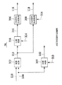
図4は、本発明によるAGC回路の第4の実施例を示すブロック図である。図4において、受信ミキサ10、SAWフィルタ12、AGC増幅器14、復調器16、可変抵抗器40、直流増幅器18、アナログフィルタ20およびアナログ・デジタル変換器(ADC)22は、CDMA無線通信装置の受信部の一部分であり、AGC増幅器14は第1のAGC回路70により制御され、可変抵抗器40は第2のAGC回路72により制御される構成となっている。なお、可変抵抗器40、直流増幅器18、アナログフィルタ20、アナログ・デジタル変換器22は、I軸信号およびQ軸信号を別々に平行して処理するものとする。また、接続線に付した参照符号はその接続線に現れる信号を示す。   FIG. 4 is a block diagram showing a fourth embodiment of the AGC circuit according to the present invention. In FIG. 4, a reception mixer 10, a SAW filter 12, an AGC amplifier 14, a demodulator 16, a variable resistor 40, a DC amplifier 18, an analog filter 20, and an analog-to-digital converter (ADC) 22 are used for receiving a CDMA radio communication device. The AGC amplifier 14 is controlled by a first AGC circuit 70, and the variable resistor 40 is controlled by a second AGC circuit 72. Note that the variable resistor 40, the DC amplifier 18, the analog filter 20, and the analog / digital converter 22 process the I-axis signal and the Q-axis signal separately and in parallel. Reference numerals attached to connection lines indicate signals appearing on the connection lines.

受信ミキサ10、SAWフィルタ12、復調器16、可変抵抗器40、直流増幅器18、アナログフィルタ20およびアナログ・デジタル変換器(ADC)22は、図1における同一の参照符号を付した構成要素と同じものである。AGC増幅器14は、第1のAGC回路から出力されるAGC電圧102に従って増幅器の利得を制御するものである。   The reception mixer 10, the SAW filter 12, the demodulator 16, the variable resistor 40, the DC amplifier 18, the analog filter 20, and the analog-to-digital converter (ADC) 22 are the same as the components denoted by the same reference numerals in FIG. Things. The AGC amplifier 14 controls the gain of the amplifier according to the AGC voltage 102 output from the first AGC circuit.

図5は、第1のAGC回路70の実施例である。この第1のAGC回路は、デジタルフィルタ24、AGC機能回路26、28およびAGC判定部30により構成され、デジタルフィルタ24およびAGC機能回路28は、図4のアナログ・デジタル変換器22に接続され、AGC判定部30は図4のAGC増幅器14に接続されている。デジタルフィルタ24は、アナログ・デジタル変換器22から出力される信号106から隣接チャネル信号成分を除去し、希望チャネル信号のデータIおよびQを選択して出力する狭帯域のローパスフィルタである。   FIG. 5 shows an embodiment of the first AGC circuit 70. The first AGC circuit includes a digital filter 24, AGC function circuits 26 and 28, and an AGC determination unit 30. The digital filter 24 and the AGC function circuit 28 are connected to the analog / digital converter 22 in FIG. The AGC determination unit 30 is connected to the AGC amplifier 14 in FIG. The digital filter 24 is a narrow-band low-pass filter that removes adjacent channel signal components from the signal 106 output from the analog-to-digital converter 22 and selects and outputs data I and Q of a desired channel signal.

デジタルフィルタ24に接続されたAGC機能回路26は、デジタルフィルタ24から出力されるデータ(データIおよびQ)を使用して、アナログ・デジタル変換器22に入力される希望チャネル信号のI軸信号およびQ軸信号の一定期間TにおけるパワーP1を計算式Σ(I2+Q2)1/2に従ってその周期T毎に算出し、パワーP1の算出値108をAGC判定部30に出力する回路である。一方、AGC機能回路28は、アナログ・デジタル変換器22から出力されるデータIおよびQを使用して、アナログ・デジタル変換器22に入力される希望チャネル信号および隣接チャネル信号の一定期間TにおけるパワーP2を計算式Σ(I2+Q2)1/2に従ってその周期T毎に算出し、パワーP2の算出値110をAGC判定部30に出力する回路である。 The AGC function circuit 26 connected to the digital filter 24 uses the data (data I and Q) output from the digital filter 24 to output the I-axis signal of the desired channel signal input to the analog / digital converter 22 and This circuit calculates the power P1 of the Q-axis signal during a certain period T according to a calculation formula 計算 (I 2 + Q 2 ) 1/2 for each period T, and outputs a calculated value 108 of the power P1 to the AGC determination unit 30. . On the other hand, the AGC function circuit 28 uses the data I and Q output from the analog-to-digital converter 22 to calculate the power of the desired channel signal and the adjacent channel signal input to the analog-to-digital converter 22 during a certain period T. P2 is a circuit that calculates P2 according to a calculation formula Σ (I 2 + Q 2 ) 1/2 for each cycle T, and outputs a calculated value 110 of power P2 to the AGC determination unit 30.

AGC機能回路26、28接続されたAGC判定部30は、AGC機能回路26から出力される算出値108とAGC機能回路28から出力される算出値110とに基づいて、AGC電圧102を生成してAGC増幅回路14に出力するものである。図6は、AGC判定部30の実施例を示すブロック図である。このAGC判定部30は、減算回路200、比較回路202、加算回路204および比較回路206から構成される。減算回路200は、図5のAGC機能回路28から出力される算出値110から、AGC機能回路26から出力される算出値108を減算して隣接チャネル信号成分のパワーP3を算出し、パワーP3を表わす算出値208を出力するものである。   The AGC determination unit 30 connected to the AGC function circuits 26 and 28 generates an AGC voltage 102 based on the calculated value 108 output from the AGC function circuit 26 and the calculated value 110 output from the AGC function circuit 28. This is output to the AGC amplifier circuit 14. FIG. 6 is a block diagram illustrating an embodiment of the AGC determination unit 30. The AGC determination unit 30 includes a subtraction circuit 200, a comparison circuit 202, an addition circuit 204, and a comparison circuit 206. The subtraction circuit 200 calculates the power P3 of the adjacent channel signal component by subtracting the calculation value 108 output from the AGC function circuit 26 from the calculation value 110 output from the AGC function circuit 28 in FIG. A calculated value 208 is output.

減算回路200に接続された比較回路202は、算出値208と予め設定された閾値210とを比較し、算出値208が閾値210より大きいときその算出値208を算出値212として出力するものである。なお、算出値208の大きさを調整して算出値212としてもよい。また、比較回路202に接続された加算回路204は、算出値108に算出値212を加算して加算値214を出力し、加算回路204に接続された比較回路206は、加算値214と予め設定された閾値216とを比較して差分値を求め、その差分値に応じて変化するAGC電圧102を生成するものである。   The comparison circuit 202 connected to the subtraction circuit 200 compares the calculated value 208 with a preset threshold value 210, and outputs the calculated value 208 as the calculated value 212 when the calculated value 208 is larger than the threshold value 210. . Note that the size of the calculated value 208 may be adjusted to be the calculated value 212. Further, the adding circuit 204 connected to the comparing circuit 202 adds the calculated value 212 to the calculated value 108 to output an added value 214, and the comparing circuit 206 connected to the adding circuit 204 sets the added value 214 in advance. The difference value is obtained by comparing the threshold value 216 with the threshold value 216, and the AGC voltage 102 that changes according to the difference value is generated.

図5に示す第1のAGC回路70の動作を説明すると、アナログ・デジタル変換器22から出力されたデータIおよびQからなるデータ106は、AGC 機能回路28およびデジタルフィルタ24に入力される。デジタルフィルタ24では、データ106の隣接チャネル信号成分の通過を阻止し、希望チャネル信号成分のみをAGC機能回路26へ出力する。AGC機能回路26では、周期T毎に計算式Σ(I2+Q2)1/2を用いて希望チャネル信号成分のパワーP1を算出する。AGC機能回路28も同様にして希望チャネル信号成分と隣接チャネル信号成分とを含む信号のパワーP2を算出する。パワーP1を示す算出値108およびパワーP2を示す算出値110は共にAGC判定部30に入力される。 The operation of the first AGC circuit 70 shown in FIG. 5 will be described. Data 106 composed of data I and Q output from the analog-to-digital converter 22 is input to the AGC function circuit 28 and the digital filter 24. The digital filter 24 prevents the adjacent channel signal components of the data 106 from passing, and outputs only the desired channel signal components to the AGC function circuit 26. The AGC function circuit 26 calculates the power P1 of the desired channel signal component using the calculation formula Σ (I 2 + Q 2 ) 1/2 for each cycle T. The AGC function circuit 28 similarly calculates the power P2 of the signal including the desired channel signal component and the adjacent channel signal component. The calculated value 108 indicating the power P1 and the calculated value 110 indicating the power P2 are both input to the AGC determination unit 30.

AGC判定部30の減算回路200では、算出値110から算出値108を減算して隣接チャネル信号成分のパワーP3を算出し、算出したP3を表わす算出値208を比較回路202へ出力する。比較回路202では、算出値208と閾値210とを比較して算出値208が閾値210より大きいとき算出値212を出力する。加算回路204では、算出値108に算出値212を加算して加算値214を出力する。したがって、加算値214は、隣接チャネル信号成分のパワーP3が閾値210より小さいときはパワーP1を表わし、閾値210を超えるときはパワーP1に隣接チャネル信号成分のパワーP3に応じて変化する算出値212を加算した値を表わすことになる。   The subtraction circuit 200 of the AGC determination unit 30 calculates the power P3 of the adjacent channel signal component by subtracting the calculated value 108 from the calculated value 110, and outputs a calculated value 208 representing the calculated P3 to the comparison circuit 202. The comparison circuit 202 compares the calculated value 208 with the threshold 210 and outputs a calculated value 212 when the calculated value 208 is larger than the threshold 210. The adding circuit 204 adds the calculated value 212 to the calculated value 108 and outputs an added value 214. Therefore, the added value 214 indicates the power P1 when the power P3 of the adjacent channel signal component is smaller than the threshold value 210, and the calculated value 212 that changes to the power P1 according to the power P3 of the adjacent channel signal component when the power P3 of the adjacent channel signal component exceeds the threshold value 210. Represents the value obtained by adding.

比較回路206では、前述のように加算回路204から出力される加算値214と閾値216とを比較してその差に応じて変化するAGC電圧102を生成してAGC増幅器14へ出力する。AGC増幅器14ではこのAGC電圧102に従って利得を制御する。   The comparison circuit 206 compares the addition value 214 output from the addition circuit 204 with the threshold value 216 as described above, generates the AGC voltage 102 that changes according to the difference, and outputs it to the AGC amplifier 14. The AGC amplifier 14 controls the gain according to the AGC voltage 102.

このように図5に示す第1のAGC回路70では、AGC判定部30により隣接チャネル信号成分のパワーP3を監視し、パワーP3が閾値210より小さい場合には、アナログ部分において隣接チャネル信号による非直線歪みの発生はないと判断し、希望チャネル信号成分のパワーP1のレベルに基づいてAGC制御を行う。これにより、アナログ・デジタル変換器22に入力される希望チャネル信号のレベルをアナログ・デジタル変換の分解能以下とならないように保持することができる。また、パワーP3が閾値210より大きい場合には、アナログ部分において隣接チャネル信号により非直線歪みの発生する恐れがあると判断し、隣接チャネル信号成分のパワーP3のレベルに応じて変化する加算値214に基づいてAGC制御を行う。これにより、アナログ部分において隣接チャネル信号により発生する信号の非直線歪みを防止することができる。   As described above, in the first AGC circuit 70 shown in FIG. 5, the power P3 of the adjacent channel signal component is monitored by the AGC determination unit 30, and when the power P3 is smaller than the threshold value 210, the non-signal due to the adjacent channel signal in the analog portion is lost. It is determined that there is no linear distortion, and AGC control is performed based on the level of the power P1 of the desired channel signal component. Thus, the level of the desired channel signal input to the analog-to-digital converter 22 can be maintained so as not to be lower than the resolution of the analog-to-digital conversion. If the power P3 is larger than the threshold 210, it is determined that there is a possibility that non-linear distortion may occur due to the adjacent channel signal in the analog portion, and the addition value 214 that changes according to the level of the power P3 of the adjacent channel signal component is determined. AGC control is performed based on. Thus, it is possible to prevent non-linear distortion of a signal generated by an adjacent channel signal in an analog portion.

なお、図6に示すAGC判定部30に代えて図7に示すAGC判定部30を用いてもよい。このAGC判定部30は、図6に示すAGC判定部30における比較回路202を省略して回路構成の簡単化を図ったものであり、減算回路200、加算回路204および比較回路206から構成される。減算回路200は、算出値110から算出値108を減算して隣接チャネル信号成分のパワーP3を算出し、これを算出値208として出力するものである。減算回路200に接続された加算回路204は、算出値108に算出値208を加算して加算値214を出力し、加算回路204に接続された比較回路206は、加算値214と予め設定された閾値216とを比較して差分値を求め、その差分値に応じて変化するAGC電圧102を生成するものである。   Note that the AGC determination unit 30 shown in FIG. 7 may be used instead of the AGC determination unit 30 shown in FIG. The AGC determination unit 30 simplifies the circuit configuration by omitting the comparison circuit 202 in the AGC determination unit 30 shown in FIG. 6 and includes a subtraction circuit 200, an addition circuit 204, and a comparison circuit 206. . The subtraction circuit 200 calculates the power P3 of the adjacent channel signal component by subtracting the calculated value 108 from the calculated value 110, and outputs this as a calculated value 208. The addition circuit 204 connected to the subtraction circuit 200 adds the calculated value 208 to the calculated value 108 and outputs an added value 214, and the comparison circuit 206 connected to the added circuit 204 is preset with the added value 214. The difference value is obtained by comparing the difference value with the threshold value 216, and the AGC voltage 102 that changes according to the difference value is generated.

図8は、図4に示す第1のAGC回路の、他の実施例を示すブロック図である。この実施例は、図5に示すAGC回路に平均処理回路32、34を追加したものであり、AGC機能回路26とAGC判定部30との間に平均処理回路32を接続し、AGC機能回路28とAGC判定部30との間に平均処理回路34を接続した構成となっている。本実施例は、このような構成によりフェージングを考慮したAGC制御を行うものである。なお、図5と同じものには同じ参照符号を付してある。   FIG. 8 is a block diagram showing another embodiment of the first AGC circuit shown in FIG. In this embodiment, the averaging circuits 32 and 34 are added to the AGC circuit shown in FIG. 5, and the averaging circuit 32 is connected between the AGC function circuit 26 and the AGC determination unit 30, and the AGC function circuit 28 An averaging circuit 34 is connected between the averaging circuit 34 and the AGC determination unit 30. In the present embodiment, AGC control considering fading is performed by such a configuration. The same components as those in FIG. 5 are denoted by the same reference numerals.

図8におけるAGC機能回路26は、パワーP1を算出してパワーP1を示す算出値108を周期T毎に平均処理回路32に出力し、AGC機能回路28は、パワーP2を算出してパワーP2を示す算出値110を周期T毎に平均処理回路34に出力する。平均処理回路34は、上記の周期Tに基づいて周期がT2(Tの整数倍)の制御パルスを生成し、この制御パルスに同期して入力される算出値108をAGC判定部30に算出値112として出力するものである。また、平均処理回路34は、上記の周期Tに基づいて周期がT2(Tの整数倍)の制御パルスを生成し、この制御パルスに同期して入力される算出値110をAGC 判定部30に算出値114として出力するものである。   The AGC function circuit 26 in FIG. 8 calculates the power P1 and outputs a calculated value 108 indicating the power P1 to the averaging circuit 32 every period T. The AGC function circuit 28 calculates the power P2 and outputs the power P2. The calculated value 110 is output to the averaging circuit 34 every period T. The averaging circuit 34 generates a control pulse having a cycle of T2 (an integer multiple of T) based on the above cycle T, and outputs a calculated value 108 input in synchronization with the control pulse to the AGC determination unit 30. It is output as 112. The averaging circuit 34 generates a control pulse having a cycle of T2 (an integral multiple of T) based on the above cycle T, and sends the calculated value 110 input in synchronization with the control pulse to the AGC determination unit 30. The calculated value 114 is output.

AGC判定部30には、平均処理回路32から算出値112が時間T1毎に入力され、平均処理回路34から算出値114が時間T2毎に入力される。本実施例のAGC判定部30は、図6に示す減算回路200の入力側にレジスタ220、222を追加した構成となっており、入力される算出値108、110をレジスタ220、222に格納し、先に格納した算出値を更新する。そして、周期T毎にレジスタ220、222から算出値108、110を読み出し、図6の場合と同様にしてAGC電圧102を生成するものである。なお、図7に示す減算回路200の入力側にレジスタ220、222を追加した構成としてもよい。   The AGC determination unit 30 receives the calculated value 112 from the averaging circuit 32 every time T1, and receives the calculated value 114 from the averaging circuit 34 every time T2. The AGC determination unit 30 of the present embodiment has a configuration in which registers 220 and 222 are added to the input side of the subtraction circuit 200 shown in FIG. 6, and stores the input calculated values 108 and 110 in the registers 220 and 222. , Update the previously stored calculated value. Then, the calculated values 108 and 110 are read from the registers 220 and 222 at each cycle T, and the AGC voltage 102 is generated in the same manner as in the case of FIG. Note that a configuration may be employed in which registers 220 and 222 are added to the input side of the subtraction circuit 200 shown in FIG.

ところで、受信部で受信される希望チャネル信号および隣接チャネル信号の受信レベルは、フェージングにより時間的に変動することが多く、通常、その変動周期はキャリア周波数により異なる。したがって、希望チャネル信号を重視し、主として希望チャネル信号のフェージングにAGCを追従させる場合には、平均処理回路32で設定される時間T1を平均処理回路34で設定される時間T2より短くすればよい。これにより、希望チャネル信号のフェージングに追従できるAGC制御を行うことが可能となる。   By the way, the reception levels of a desired channel signal and an adjacent channel signal received by the receiving unit often fluctuate with time due to fading, and the fluctuation cycle usually differs depending on the carrier frequency. Therefore, when emphasizing the desired channel signal and mainly causing the AGC to follow the fading of the desired channel signal, the time T1 set by the averaging circuit 32 may be shorter than the time T2 set by the averaging circuit 34. . This makes it possible to perform AGC control that can follow fading of a desired channel signal.

図9は、図4に示す第1のAGC回路の、さらに他の実施例を示すブロック図である。この実施例は、図5に示す第1のAGC回路におけるAGC判定部30をAGC判定部36に置き換え、このAGC判定部36と直流増幅器18との間に制御回路38を接続したものである。本実施例は、このような構成により隣接チャネル信号が所定のレベル以上に増大したとき、直流増幅回路18の可変アッテネータの減衰量を瞬時に増大させてアナログ部における非直線歪みの発生を迅速に防止する。なお、直流増幅器18はI軸信号およびQ軸信号を別々に平行して処理するものとする。また、図5と同じものには同じ参照符号を付してある。   FIG. 9 is a block diagram showing still another embodiment of the first AGC circuit shown in FIG. In this embodiment, the AGC determination unit 30 in the first AGC circuit shown in FIG. 5 is replaced with an AGC determination unit 36, and a control circuit 38 is connected between the AGC determination unit 36 and the DC amplifier 18. According to this embodiment, when the adjacent channel signal increases to a predetermined level or more due to such a configuration, the amount of attenuation of the variable attenuator of the DC amplifier circuit 18 is instantaneously increased, and the generation of nonlinear distortion in the analog section is quickly performed. To prevent. The DC amplifier 18 processes the I-axis signal and the Q-axis signal separately and in parallel. The same components as those in FIG. 5 are denoted by the same reference numerals.

図9におけるAGC判定部36は、AGC機能回路26、28から出力される算出値108、110に基づいてAGC 増幅器14に供給するAGC電圧102 を生成すると共に、制御回路38に出力するEN信号116およびSW信号118を生成するものである。図10は、このAGC判定部36の実施例を示すブロック図である。この実施例のAGC判定部36は、比較回路300、減算回路302、比較回路304、EN信号生成回路306およびSW信号生成回路308から構成される。   9 generates an AGC voltage 102 to be supplied to the AGC amplifier 14 based on the calculated values 108 and 110 output from the AGC function circuits 26 and 28, and an EN signal 116 output to the control circuit 38. And the SW signal 118 are generated. FIG. 10 is a block diagram showing an embodiment of the AGC determination unit 36. The AGC determination unit 36 of this embodiment includes a comparison circuit 300, a subtraction circuit 302, a comparison circuit 304, an EN signal generation circuit 306, and a SW signal generation circuit 308.

比較回路300は、AGC機能回路26から出力される算出値108と予め設定された閾値310とを比較してその差に応じて変化するAGC電圧102を生成してAGC増幅器14に出力するものである。減算回路302は、AGC機能回路28から出力される算出値110から、AGC機能回路26から出力される算出値108を減算して隣接チャネル信号成分のパワーP3を算出し、パワーP3を示す算出値312を出力するものである。減算回路302に接続された比較回路304は、算出値312と予め設定された閾値314とを比較し、算出値312が閾値314を超えた時および算出値312が閾値314より下がった時に起動信号316を出力するものである。   The comparison circuit 300 compares the calculated value 108 output from the AGC function circuit 26 with a preset threshold 310, generates an AGC voltage 102 that changes according to the difference, and outputs the generated AGC voltage 102 to the AGC amplifier 14. is there. The subtraction circuit 302 calculates the power P3 of the adjacent channel signal component by subtracting the calculation value 108 output from the AGC function circuit 26 from the calculation value 110 output from the AGC function circuit 28, and calculates the power P3 312 is output. The comparison circuit 304 connected to the subtraction circuit 302 compares the calculated value 312 with a preset threshold value 314, and when the calculated value 312 exceeds the threshold value 314 and when the calculated value 312 falls below the threshold value 314, the activation signal 316 is output.

また、比較回路304に接続されたEN信号生成回路306は、比較回路304から起動信号316が与えられたとき、減衰量の切り替えを指示するEN信号116を生成するものである。減算回路302 に接続されたSW信号生成回路308は、減算回路302から出力される算出値312が閾値314より小さいとき直流増幅器18のアッテネータを第1の減衰量に設定し、大きいとき第2の減衰量に設定するSW信号118を生成するものである。ここで、第2の減衰量は第1の減衰量より大きいものとする。EN信号116およびSW信号118は図5の制御回路38に入力される。   Further, the EN signal generation circuit 306 connected to the comparison circuit 304 generates the EN signal 116 instructing the switching of the attenuation when the start signal 316 is given from the comparison circuit 304. The SW signal generation circuit 308 connected to the subtraction circuit 302 sets the attenuator of the DC amplifier 18 to the first attenuation when the calculated value 312 output from the subtraction circuit 302 is smaller than the threshold 314, and sets the second attenuation when the calculated value 312 is larger than the threshold 314. This is to generate the SW signal 118 for setting the amount of attenuation. Here, it is assumed that the second attenuation is larger than the first attenuation. The EN signal 116 and the SW signal 118 are input to the control circuit 38 of FIG.

制御回路38は、タイミングクロック生成回路とSW信号出力回路とを含む(いずれも図示せず)。そして、タイミングクロック生成回路は、アナログ・デジタル変換器22に供給されるサンプリングクロック120より1/2サンプリングクロックずれたタイミングクロックを生成し、AGC判定部36からEN信号116 が与えられたときこのタイミングクロックに同期する切替タイミング信号を生成する。また、SW信号出力回路は、タイミングクロック生成回路で切替タイミング信号が生成されたとき、AGC判定部36から与えられるSW信号118をSW切替信号122として直流増幅器18に出力する。したがって、直流増幅器18における可変アッテネータの減衰量の切り替えは、サンプリングクロック120の中間点で実行され、アナログ・デジタル変換器22で行われるサンプリング動作に影響を及すことはない。   The control circuit 38 includes a timing clock generation circuit and a SW signal output circuit (neither is shown). Then, the timing clock generation circuit generates a timing clock which is shifted by 1/2 sampling clock from the sampling clock 120 supplied to the analog / digital converter 22, and when the EN signal 116 is given from the AGC determination unit 36, the timing clock is generated. A switching timing signal synchronized with the clock is generated. Further, when the switching clock signal is generated by the timing clock generation circuit, the SW signal output circuit outputs the SW signal 118 given from the AGC determination unit 36 to the DC amplifier 18 as the SW switching signal 122. Therefore, the switching of the attenuation of the variable attenuator in the DC amplifier 18 is performed at the intermediate point of the sampling clock 120, and does not affect the sampling operation performed by the analog / digital converter 22.

また、本実施例の直流増幅回路18は、入力信号に減衰を与える可変アッテネータを有し、制御回路38から与えられるSW切替信号122に従って可変アッテネータの減衰量を第1の減衰量または第2の減衰量に切り替えるものである。この可変アッテネータは、抵抗素子および切替スイッチから構成されており、時定数回路を含まないので減衰量の設定を迅速に切り替えることができる。なお、I軸信号およびQ軸信号に与える減衰量は共に、SW切替信号122に従うものとする。   Further, the DC amplification circuit 18 of the present embodiment has a variable attenuator that attenuates the input signal, and adjusts the attenuation of the variable attenuator to the first attenuation amount or the second attenuation amount according to the SW switching signal 122 provided from the control circuit 38. It is switched to the amount of attenuation. This variable attenuator is composed of a resistance element and a changeover switch, and does not include a time constant circuit, so that the setting of the attenuation can be quickly switched. It is assumed that the amount of attenuation applied to the I-axis signal and the Q-axis signal both follow the SW switching signal 122.

本実施例の動作を説明すると、AGC回路のAGC判定部36では、希望チャネル信号成分のパワーP1に基づいてAGC 電圧102を生成してAGC増幅器14に出力する。また、AGC判定部36では、AGC電圧102 の生成と並行して隣接チャネル信号成分のパワーP3を監視し、パワーP3が所定の閾値を超えた時に第2の減衰量を設定し、パワーP3が所定の閾値より下がった時に第1の減衰量を設定するSW信号118を生成すると共に減衰量の切り替えを指示するEN信号116を生成して制御回路38に出力する。   The operation of the present embodiment will be described. The AGC determination unit 36 of the AGC circuit generates an AGC voltage 102 based on the power P1 of the desired channel signal component and outputs it to the AGC amplifier 14. In addition, the AGC determination unit 36 monitors the power P3 of the adjacent channel signal component in parallel with the generation of the AGC voltage 102, and sets a second attenuation when the power P3 exceeds a predetermined threshold. When the voltage falls below a predetermined threshold value, an SW signal 118 for setting the first attenuation is generated, and an EN signal 116 for instructing the switching of the attenuation is generated and output to the control circuit.

AGC増幅器14では、AGC判定部36から供給されるAGC電圧102に従って利得を制御する。一方、制御回路38では、AGC 判定部36からEN信号116およびSW信号118が与えられたとき、サンプリングクロック120より1/2サンプリングクロックだけずれたタイミングでSW切替信号122を直流増幅器18に出力する。直流増幅器18では、このSW切替信号122に従って可変アッテネータの減衰量を切り替える。   The AGC amplifier 14 controls the gain according to the AGC voltage 102 supplied from the AGC determination unit 36. On the other hand, in the control circuit 38, when the EN signal 116 and the SW signal 118 are given from the AGC determination unit 36, the control circuit 38 outputs the SW switching signal 122 to the DC amplifier 18 at a timing shifted by 1/2 sampling clock from the sampling clock 120. . The DC amplifier 18 switches the attenuation of the variable attenuator according to the SW switching signal 122.

このように図9に示す第1のAGC回路によれば、直流増幅器18に時定数を含まない可変アッテネータを設け、隣接チャネル信号成分のパワーP3に応じて可変アッテネータの減衰量を切り替えているので、パワーP3のレベル変動に迅速に対応することができる。   As described above, according to the first AGC circuit shown in FIG. 9, a variable attenuator not including a time constant is provided in the DC amplifier 18, and the attenuation of the variable attenuator is switched according to the power P3 of the adjacent channel signal component. , Can quickly respond to the level fluctuation of the power P3.

図4における第2のAGC回路72は、可変抵抗器40における減衰量を制御する回路であり、図1に示すAGC回路、図2に示すAGC回路および図3に示すAGC回路のいずれを適用してもよい。ただし、図1および図2に示すAGC回路を適用する場合には、アナログフィルタ20から出力される信号130をAGC回路に入力し、図3に示すAGC回路を適用する場合には、直流増幅器18から出力される信号160をAGC回路に入力する。   The second AGC circuit 72 in FIG. 4 is a circuit for controlling the amount of attenuation in the variable resistor 40, and employs any of the AGC circuit shown in FIG. 1, the AGC circuit shown in FIG. 2, and the AGC circuit shown in FIG. May be. However, when the AGC circuit shown in FIGS. 1 and 2 is applied, the signal 130 output from the analog filter 20 is input to the AGC circuit, and when the AGC circuit shown in FIG. Is input to the AGC circuit.

図4の第4の実施例によれば、第1のAGC回路70によりAGC増幅器14の利得を制御しているので、アナログ・デジタル変換器22に入力される希望チャネル信号のレベルをアナログ・デジタル変換の分解能以下とならないように保持することができ、アナログ部分において非直線歪みが発生しないようにすることができる。また、第1のAGC回路70によるAGC増幅器14の利得制御には一定の応答時間を必要とするが、第2のAGC回路72により可変抵抗器40または直流増幅器における可変アッテネータを制御しているので、隣接チャネル成分のレベルが急激に変化した場合でも、非直線歪みの発生を迅速に防止することができる。   According to the fourth embodiment of FIG. 4, since the gain of the AGC amplifier 14 is controlled by the first AGC circuit 70, the level of the desired channel signal input to the analog-to-digital The resolution can be maintained so as not to be lower than the resolution of the conversion, and non-linear distortion can be prevented from occurring in the analog portion. The gain control of the AGC amplifier 14 by the first AGC circuit 70 requires a certain response time. However, since the second AGC circuit 72 controls the variable resistor 40 or the variable attenuator in the DC amplifier, In addition, even when the level of the adjacent channel component changes suddenly, it is possible to quickly prevent the occurrence of nonlinear distortion.

本発明によるAGC回路の第1の実施例を示すブロック図である。FIG. 2 is a block diagram showing a first embodiment of the AGC circuit according to the present invention. 本発明によるAGC回路の第2の実施例を示すブロック図である。FIG. 6 is a block diagram showing a second embodiment of the AGC circuit according to the present invention. 本発明によるAGC回路の第3の実施例を示すブロック図である。FIG. 9 is a block diagram showing a third embodiment of the AGC circuit according to the present invention. 本発明によるAGC回路の第4の実施例を示すブロック図である。FIG. 11 is a block diagram showing a fourth embodiment of the AGC circuit according to the present invention. 図4に示す第1のAGC回路の実施例を示すブロック図である。FIG. 5 is a block diagram showing an example of the first AGC circuit shown in FIG. 図5に示すAGC判定部の実施例を示すブロック図である。FIG. 6 is a block diagram illustrating an example of an AGC determination unit illustrated in FIG. 5. 図5に示すAGC 判定部の他の実施例を示すブロック図である。FIG. 13 is a block diagram illustrating another embodiment of the AGC determination unit illustrated in FIG. 5. 図4に示す第1のAGC 回路の他の実施例を示すブロック図である。FIG. 10 is a block diagram showing another embodiment of the first AGC circuit shown in FIG. 第1のAGC 回路のさらに他の実施例を示すブロック図である。FIG. 11 is a block diagram showing still another embodiment of the first AGC circuit. 図9に示すAGC 回路のAGC 判定部の実施例を示すブロック図である。10 is a block diagram illustrating an embodiment of an AGC determination unit of the AGC circuit illustrated in FIG.

符号の説明Explanation of reference numerals

14 AGC増幅器
16 復調器
20、42、54 アナログフィルタ
22 アナログ・デジタル変換器
40 可変抵抗器
44 遅延回路
46 可変利得増幅器
48 差動増幅器
50、60 比較器
52 EN信号発生器
58 ピーク検知器
70 第1のAGC回路
72 第2のAGC回路
14 AGC amplifier
16 demodulator
20, 42, 54 Analog filter
22 Analog-to-digital converter
40 Variable resistor
44 Delay circuit
46 Variable gain amplifier
48 Differential amplifier
50, 60 comparator
52 EN signal generator
58 Peak detector
70 First AGC Circuit
72 Second AGC circuit

Claims (5)

直交変調された受信信号を復調してI軸信号およびQ軸信号を出力する復調器と、切替信号に従って減衰量を第1の減衰量または該第1の減衰量より大きい第2の減衰量に切り替えて前記復調器から出力されるI軸信号およびQ軸信号に減衰を与える可変抵抗器と、該可変抵抗器から出力されるI軸信号およびQ軸信号の希望チャネル信号成分を通過させる第1のアナログフィルタと、該第1のアナログフィルタから出力されるI軸信号およびQ軸信号をデータに変換するアナログ・デジタル変換器とを含む無線装置受信部の自動利得制御回路において、該回路は、
前記第1のアナログフィルタから出力されるI軸信号およびQ軸信号の希望チャネル信号成分を通過させる第2のアナログフィルタと、
該第2のアナログフィルタから出力されるI軸信号およびQ軸信号に所定の遅延を与える遅延手段と、
該遅延手段を通過した信号のレベルを調整する可変利得増幅手段と、
該可変利得増幅手段から出力される信号から、前記第2のアナログフィルタから出力される信号を減算して隣接チャネル信号成分を算出し、該隣接チャネル信号成分が閾値を超えた時前記可変抵抗器の減衰量を第2の減衰量に切り替え、該隣接チャネル信号成分が前記閾値より低下した時前記可変抵抗器の減衰量を第1の減衰量に切り替える前記切替信号を生成する比較手段とを含むことを特徴とする自動利得制御回路。
A demodulator that demodulates a quadrature-modulated received signal and outputs an I-axis signal and a Q-axis signal, and sets the attenuation to a first attenuation or a second attenuation larger than the first attenuation according to a switching signal. A variable resistor for switching to attenuate an I-axis signal and a Q-axis signal output from the demodulator, and a first resistor for passing desired channel signal components of the I-axis signal and the Q-axis signal output from the variable resistor. And an analog-to-digital converter for converting the I-axis signal and the Q-axis signal output from the first analog filter into data.
A second analog filter that passes desired channel signal components of the I-axis signal and the Q-axis signal output from the first analog filter;
Delay means for giving a predetermined delay to the I-axis signal and the Q-axis signal output from the second analog filter;
Variable gain amplifying means for adjusting the level of the signal passing through the delay means,
The signal output from the second analog filter is subtracted from the signal output from the variable gain amplifying means to calculate an adjacent channel signal component. When the adjacent channel signal component exceeds a threshold value, the variable resistor And a comparing means for generating the switching signal for switching the attenuation of the variable resistor to the first attenuation when the adjacent channel signal component falls below the threshold. An automatic gain control circuit, characterized in that:
直交変調された受信信号を復調してI軸信号およびQ軸信号を出力する復調器と、切替信号に従って減衰量を第1の減衰量または該第1の減衰量より大きい第2の減衰量に切り替えて前記復調器から出力されるI軸信号およびQ軸信号に減衰を与える可変抵抗器と、該可変抵抗器から出力されるI軸信号およびQ軸信号の希望チャネル信号成分を通過させる第1のアナログフィルタと、該第1のアナログフィルタから出力されるI軸信号およびQ軸信号をデータに変換するアナログ・デジタル変換器とを含む無線装置受信部の自動利得制御回路において、該回路は、
前記第1のアナログフィルタから出力されるI軸信号およびQ軸信号の隣接チャネル信号成分を通過させる第3のアナログフィルタと、
該第3のアナログフィルタから出力されるI軸信号およびQ軸信号の隣接チャネル信号成分が閾値を超えた時前記可変抵抗器の減衰量を第2の減衰量に切り替え、該隣接チャネル信号成分が前記閾値より低下した時前記可変抵抗器の減衰量を第1の減衰量に切り替える前記切替信号を生成する比較手段とを含むことを特徴とする自動利得制御回路。
A demodulator that demodulates a quadrature-modulated received signal and outputs an I-axis signal and a Q-axis signal, and sets the attenuation to a first attenuation or a second attenuation larger than the first attenuation according to a switching signal. A variable resistor for switching to attenuate an I-axis signal and a Q-axis signal output from the demodulator, and a first resistor for passing desired channel signal components of the I-axis signal and the Q-axis signal output from the variable resistor. And an analog-to-digital converter for converting the I-axis signal and the Q-axis signal output from the first analog filter into data.
A third analog filter that passes adjacent channel signal components of the I-axis signal and the Q-axis signal output from the first analog filter;
When the adjacent channel signal components of the I-axis signal and the Q-axis signal output from the third analog filter exceed a threshold, the attenuation of the variable resistor is switched to the second attenuation, and the adjacent channel signal component is An automatic gain control circuit, comprising: a comparing unit that generates the switching signal that switches the amount of attenuation of the variable resistor to a first amount of attenuation when the voltage falls below the threshold value.
直交変調された受信信号を復調してI軸信号およびQ軸信号を出力する復調器と、切替信号に従って減衰量を第1の減衰量または該第1の減衰量より大きい第2の減衰量に切り替えて前記復調器から出力されるI軸信号およびQ軸信号に減衰を与える可変抵抗器と、該可変抵抗器から出力されるI軸信号およびQ軸信号をそれぞれ増幅する直流増幅器と、該直流増幅器から出力されるI軸信号およびQ軸信号の希望チャネル信号成分を通過させる第1のアナログフィルタと、該第1のアナログフィルタから出力されるI軸信号およびQ軸信号をデータに変換するアナログ・デジタル変換器とを含む無線装置受信部の自動利得制御回路において、該回路は、
前記直流増幅器から出力されるI軸信号およびQ軸信号からなる信号のピーク値を検知するピーク検知手段と、
該ピーク検知手段で検知されたピーク値が予め定められた時間連続して閾値を超える時前記可変抵抗器の減衰量を第2の減衰量に切り替え、前記ピーク値が前期時間連続して前記閾値を超えない時前記可変抵抗器の減衰量を第1の減衰量に切り替える前記切替信号を生成する比較手段とを含むことを特徴とする自動利得制御回路。
A demodulator that demodulates a quadrature-modulated received signal and outputs an I-axis signal and a Q-axis signal, and sets the attenuation to a first attenuation or a second attenuation larger than the first attenuation according to a switching signal. A variable resistor that switches to attenuate an I-axis signal and a Q-axis signal output from the demodulator, a DC amplifier that amplifies the I-axis signal and the Q-axis signal output from the variable resistor, A first analog filter that passes desired channel signal components of an I-axis signal and a Q-axis signal output from an amplifier, and an analog that converts the I-axis signal and the Q-axis signal output from the first analog filter into data An automatic gain control circuit of a wireless device receiving unit including a digital converter;
Peak detection means for detecting a peak value of a signal consisting of an I-axis signal and a Q-axis signal output from the DC amplifier;
When the peak value detected by the peak detecting means continuously exceeds a threshold for a predetermined time, the attenuation of the variable resistor is switched to the second attenuation, and the peak value is continuously changed to the threshold for the first time. And a comparing means for generating the switching signal for switching the amount of attenuation of the variable resistor to the first amount of attenuation when not exceeding.
請求項1ないし3のいずれかに記載の自動利得制御回路において、該回路はさらに、前記AGC増幅器の前段に設けられたAGC増幅器と該AGC増幅器へAGC電圧を供給して利得を制御するAGC回路とを含み、
該AGC回路は、前記アナログ・デジタル変換器から出力されるI軸信号およびQ軸信号の各デジタル信号の希望チャネル信号成分をそれぞれ通過させるデジタルフィルタと、
該デジタルフィルタを通過した各デジタル信号の希望チャネル信号成分の合計パワーを第1の期間毎に算出する第1のAGC機能手段と、
前記アナログ・デジタル変換器でデジタル化されたI軸信号およびQ軸信号の各デジタル信号の合計パワーを前記第1の期間毎に算出する第2のAGC機能手段と、
該第2のAGC機能手段で算出されたパワーから前記第1のAGC機能手段で算出されたパワーを減算して隣接チャネル信号成分のパワーを算出し、該隣接チャネル信号成分のパワーが閾値より小さい場合は、前記第1のAGC機能手段で算出されたパワーに応じて変化する前記AGC電圧を生成し、隣接チャネル信号成分のパワーが前記閾値より大きい場合は、前記第1のAGC機能手段で算出されたパワーと前記隣接チャネル信号成分のパワーとを含むパワーに応じて変化する前記AGC電圧を生成するAGC判定手段とを含むことを特徴とする自動利得制御回路。
4. The automatic gain control circuit according to claim 1, further comprising an AGC amplifier provided in a stage preceding said AGC amplifier, and an AGC circuit for supplying an AGC voltage to said AGC amplifier to control a gain. And
The AGC circuit includes a digital filter that passes a desired channel signal component of each digital signal of the I-axis signal and the Q-axis signal output from the analog-to-digital converter,
First AGC function means for calculating a total power of a desired channel signal component of each digital signal passed through the digital filter for each first period;
Second AGC function means for calculating a total power of each digital signal of the I-axis signal and the Q-axis signal digitized by the analog-to-digital converter for each of the first periods;
The power of the adjacent channel signal component is calculated by subtracting the power calculated by the first AGC function unit from the power calculated by the second AGC function unit, and the power of the adjacent channel signal component is smaller than a threshold. In the case, the AGC voltage that changes according to the power calculated by the first AGC function means is generated, and when the power of the adjacent channel signal component is larger than the threshold, the AGC voltage is calculated by the first AGC function means. An automatic gain control circuit comprising: an AGC determining unit that generates the AGC voltage that changes in accordance with a power including the determined power and the power of the adjacent channel signal component.
請求項1ないし3のいずれかに記載の自動利得制御回路において、前記可変抵抗器における減衰量の切り替えは、前記アナログ・デジタル変換器に供給されるサンプリングクロックの周期の中間点で行うことを特徴とする自動利得制御回路。 4. The automatic gain control circuit according to claim 1, wherein the switching of the amount of attenuation in the variable resistor is performed at an intermediate point of a cycle of a sampling clock supplied to the analog-to-digital converter. Automatic gain control circuit.
JP2004046220A 2004-02-23 2004-02-23 Automatic gain control circuit Expired - Fee Related JP4123166B2 (en)

Priority Applications (1)

Application Number Priority Date Filing Date Title
JP2004046220A JP4123166B2 (en) 2004-02-23 2004-02-23 Automatic gain control circuit

Applications Claiming Priority (1)

Application Number Priority Date Filing Date Title
JP2004046220A JP4123166B2 (en) 2004-02-23 2004-02-23 Automatic gain control circuit

Related Parent Applications (1)

Application Number Title Priority Date Filing Date
JP2002176740A Division JP3586267B2 (en) 2002-06-18 2002-06-18 Automatic gain control circuit

Publications (2)

Publication Number Publication Date
JP2004194355A true JP2004194355A (en) 2004-07-08
JP4123166B2 JP4123166B2 (en) 2008-07-23

Family

ID=32768223

Family Applications (1)

Application Number Title Priority Date Filing Date
JP2004046220A Expired - Fee Related JP4123166B2 (en) 2004-02-23 2004-02-23 Automatic gain control circuit

Country Status (1)

Country Link
JP (1) JP4123166B2 (en)

Cited By (6)

* Cited by examiner, † Cited by third party
Publication number Priority date Publication date Assignee Title
KR100727814B1 (en) 2005-12-08 2007-06-13 한국전자통신연구원 Auto gain control circuit and wireless reciever comprising it
US7933369B2 (en) 2005-12-08 2011-04-26 Electronics And Telecommunications Research Institute Apparatus for automatic gain control and wireless receiver employing the same
WO2013190806A1 (en) * 2012-06-21 2013-12-27 日本電気株式会社 Automatic gain control device, automatic gain control method, and computer-readable medium
US10594282B2 (en) * 2017-01-27 2020-03-17 Lapis Semiconductor Co., Ltd. Automatic gain control (AGC) circuit, despreading circuit, and method for reproducing reception data
CN113839635A (en) * 2021-09-29 2021-12-24 四川安迪科技实业有限公司 Anti-interference self-adaptive AGC (automatic gain control) adjusting method and device based on smooth filtering
CN114221668A (en) * 2021-12-20 2022-03-22 湖南迈克森伟电子科技有限公司 Adaptive power gain control method and receiver

Cited By (8)

* Cited by examiner, † Cited by third party
Publication number Priority date Publication date Assignee Title
KR100727814B1 (en) 2005-12-08 2007-06-13 한국전자통신연구원 Auto gain control circuit and wireless reciever comprising it
US7933369B2 (en) 2005-12-08 2011-04-26 Electronics And Telecommunications Research Institute Apparatus for automatic gain control and wireless receiver employing the same
WO2013190806A1 (en) * 2012-06-21 2013-12-27 日本電気株式会社 Automatic gain control device, automatic gain control method, and computer-readable medium
JPWO2013190806A1 (en) * 2012-06-21 2016-02-08 日本電気株式会社 Automatic gain control device, automatic gain control method, and automatic gain control program
US10594282B2 (en) * 2017-01-27 2020-03-17 Lapis Semiconductor Co., Ltd. Automatic gain control (AGC) circuit, despreading circuit, and method for reproducing reception data
CN113839635A (en) * 2021-09-29 2021-12-24 四川安迪科技实业有限公司 Anti-interference self-adaptive AGC (automatic gain control) adjusting method and device based on smooth filtering
CN113839635B (en) * 2021-09-29 2023-06-20 四川安迪科技实业有限公司 Anti-interference self-adaptive AGC (automatic gain control) adjusting method and device based on smooth filtering
CN114221668A (en) * 2021-12-20 2022-03-22 湖南迈克森伟电子科技有限公司 Adaptive power gain control method and receiver

Also Published As

Publication number Publication date
JP4123166B2 (en) 2008-07-23

Similar Documents

Publication Publication Date Title
JP4072061B2 (en) DC offset correction method for wireless receiver
JP4834806B2 (en) Method and apparatus for dynamic gain and phase compensation
KR100615022B1 (en) A wireless receiver and a method of processing wireless signal
US7203476B2 (en) Method and apparatus for minimizing baseband offset error in a receiver
JP2006121146A (en) Filter control apparatus and method of wireless receiver, and integrated circuit for wireless receiver employing the same
KR970013823A (en) A radio receiver including a variable gain amplifier circuit, an offset control method in a variable gain amplifier circuit, a radio receiver including a variable gain amplifier circuit, and a radio receiver including a variable gain amplifier circuit, the radio receiver including a VARIABLE GAIN AMPLIFIER CIRCUIT, an OFFSET CONTROL METHOD IN VARIABLE GAIN AMPLIFIER CIRCUIT, WIRELESS RECEIVER HAVING A VARIABLE GAIN AMPLIFIER CIRCUIT, WIRELESS RECEIVING METHOD IN A WIRELESS RECEIVER HAVING A VARIABLE GAIN AMPLIFIER CIRCUIT)
US20080090545A1 (en) Signal Processing Unit
EP1061643B1 (en) Receiver and gain control method of the same
JP2001044860A (en) Receiver provided with automatic gain control circuit
JP3586267B2 (en) Automatic gain control circuit
US20080170606A1 (en) Method and apparatus for providing a digital automatic gain control (AGC)
JP2004147000A (en) Agc system
JP2004194355A (en) Automatic gain control circuit
JP4422116B2 (en) AGC control method and AGC circuit
JP2009182589A (en) Rf receiver
JP3468264B2 (en) Offset compensation circuit and method
JPWO2007032550A1 (en) Reception amplitude correction circuit, reception amplitude correction method, and receiver using the same
JP4933624B2 (en) Wireless receiver
KR100499523B1 (en) RF Signal Gain controller
JP2005101693A (en) Receiver
JP2001086176A (en) Digital transmitter-receiver
KR100309376B1 (en) Apparatus for controling gain of baseband signal in cdma mobile communication system
JPWO2006098325A1 (en) Noise canceller
US20080130607A1 (en) Method and System for Multimode DC Offset Compensation
JP4927054B2 (en) FM signal noise canceller circuit

Legal Events

Date Code Title Description
A977 Report on retrieval

Free format text: JAPANESE INTERMEDIATE CODE: A971007

Effective date: 20060112

A131 Notification of reasons for refusal

Free format text: JAPANESE INTERMEDIATE CODE: A131

Effective date: 20060411

A521 Written amendment

Free format text: JAPANESE INTERMEDIATE CODE: A523

Effective date: 20060607

A131 Notification of reasons for refusal

Effective date: 20070403

Free format text: JAPANESE INTERMEDIATE CODE: A131

A521 Written amendment

Free format text: JAPANESE INTERMEDIATE CODE: A523

Effective date: 20070425

TRDD Decision of grant or rejection written
A01 Written decision to grant a patent or to grant a registration (utility model)

Free format text: JAPANESE INTERMEDIATE CODE: A01

Effective date: 20080408

A01 Written decision to grant a patent or to grant a registration (utility model)

Free format text: JAPANESE INTERMEDIATE CODE: A01

A61 First payment of annual fees (during grant procedure)

Effective date: 20080421

Free format text: JAPANESE INTERMEDIATE CODE: A61

R150 Certificate of patent (=grant) or registration of utility model

Free format text: JAPANESE INTERMEDIATE CODE: R150

FPAY Renewal fee payment (prs date is renewal date of database)

Year of fee payment: 3

Free format text: PAYMENT UNTIL: 20110516

FPAY Renewal fee payment (prs date is renewal date of database)

Free format text: PAYMENT UNTIL: 20110516

Year of fee payment: 3

S111 Request for change of ownership or part of ownership

Free format text: JAPANESE INTERMEDIATE CODE: R313111

S531 Written request for registration of change of domicile

Free format text: JAPANESE INTERMEDIATE CODE: R313531

FPAY Renewal fee payment (prs date is renewal date of database)

Year of fee payment: 3

Free format text: PAYMENT UNTIL: 20110516

R350 Written notification of registration of transfer

Free format text: JAPANESE INTERMEDIATE CODE: R350

FPAY Renewal fee payment (prs date is renewal date of database)

Free format text: PAYMENT UNTIL: 20110516

Year of fee payment: 3

FPAY Renewal fee payment (prs date is renewal date of database)

Free format text: PAYMENT UNTIL: 20120516

Year of fee payment: 4

LAPS Cancellation because of no payment of annual fees