JP2004191982A - Method for forming optical converter - Google Patents
Method for forming optical converter Download PDFInfo
- Publication number
- JP2004191982A JP2004191982A JP2003409137A JP2003409137A JP2004191982A JP 2004191982 A JP2004191982 A JP 2004191982A JP 2003409137 A JP2003409137 A JP 2003409137A JP 2003409137 A JP2003409137 A JP 2003409137A JP 2004191982 A JP2004191982 A JP 2004191982A
- Authority
- JP
- Japan
- Prior art keywords
- fiber
- ribbon
- output
- edge
- input
- Prior art date
- Legal status (The legal status is an assumption and is not a legal conclusion. Google has not performed a legal analysis and makes no representation as to the accuracy of the status listed.)
- Pending
Links
Images


Classifications
-
- G—PHYSICS
- G02—OPTICS
- G02B—OPTICAL ELEMENTS, SYSTEMS OR APPARATUS
- G02B6/00—Light guides; Structural details of arrangements comprising light guides and other optical elements, e.g. couplings
- G02B6/04—Light guides; Structural details of arrangements comprising light guides and other optical elements, e.g. couplings formed by bundles of fibres
-
- H—ELECTRICITY
- H10—SEMICONDUCTOR DEVICES; ELECTRIC SOLID-STATE DEVICES NOT OTHERWISE PROVIDED FOR
- H10K—ORGANIC ELECTRIC SOLID-STATE DEVICES
- H10K50/00—Organic light-emitting devices
- H10K50/80—Constructional details
-
- H—ELECTRICITY
- H10—SEMICONDUCTOR DEVICES; ELECTRIC SOLID-STATE DEVICES NOT OTHERWISE PROVIDED FOR
- H10K—ORGANIC ELECTRIC SOLID-STATE DEVICES
- H10K50/00—Organic light-emitting devices
- H10K50/80—Constructional details
- H10K50/85—Arrangements for extracting light from the devices
-
- H—ELECTRICITY
- H10—SEMICONDUCTOR DEVICES; ELECTRIC SOLID-STATE DEVICES NOT OTHERWISE PROVIDED FOR
- H10K—ORGANIC ELECTRIC SOLID-STATE DEVICES
- H10K59/00—Integrated devices, or assemblies of multiple devices, comprising at least one organic light-emitting element covered by group H10K50/00
- H10K59/10—OLED displays
- H10K59/18—Tiled displays
-
- Y—GENERAL TAGGING OF NEW TECHNOLOGICAL DEVELOPMENTS; GENERAL TAGGING OF CROSS-SECTIONAL TECHNOLOGIES SPANNING OVER SEVERAL SECTIONS OF THE IPC; TECHNICAL SUBJECTS COVERED BY FORMER USPC CROSS-REFERENCE ART COLLECTIONS [XRACs] AND DIGESTS
- Y10—TECHNICAL SUBJECTS COVERED BY FORMER USPC
- Y10T—TECHNICAL SUBJECTS COVERED BY FORMER US CLASSIFICATION
- Y10T156/00—Adhesive bonding and miscellaneous chemical manufacture
- Y10T156/10—Methods of surface bonding and/or assembly therefor
- Y10T156/1002—Methods of surface bonding and/or assembly therefor with permanent bending or reshaping or surface deformation of self sustaining lamina
- Y10T156/1007—Running or continuous length work
- Y10T156/1015—Folding
-
- Y—GENERAL TAGGING OF NEW TECHNOLOGICAL DEVELOPMENTS; GENERAL TAGGING OF CROSS-SECTIONAL TECHNOLOGIES SPANNING OVER SEVERAL SECTIONS OF THE IPC; TECHNICAL SUBJECTS COVERED BY FORMER USPC CROSS-REFERENCE ART COLLECTIONS [XRACs] AND DIGESTS
- Y10—TECHNICAL SUBJECTS COVERED BY FORMER USPC
- Y10T—TECHNICAL SUBJECTS COVERED BY FORMER US CLASSIFICATION
- Y10T156/00—Adhesive bonding and miscellaneous chemical manufacture
- Y10T156/10—Methods of surface bonding and/or assembly therefor
- Y10T156/1002—Methods of surface bonding and/or assembly therefor with permanent bending or reshaping or surface deformation of self sustaining lamina
- Y10T156/1051—Methods of surface bonding and/or assembly therefor with permanent bending or reshaping or surface deformation of self sustaining lamina by folding
Abstract
Description
本発明は、一般的に画像形成システム用光変換器として使用される光ファイバーフェースプレートの製造に関し、より詳細には複数の光ガイドを含む可撓性ストリップから製造された光ファイバーフェースプレートに関する。 The present invention relates generally to the manufacture of fiber optic faceplates used as light converters for imaging systems, and more particularly to fiber optic faceplates made from flexible strips that include multiple light guides.
電子表示システムの一つの利点として、種々のフォーマット及びサイズの画像を表示することができる点があげられる。かなりの距離から数千人のビューアが見ることができる大型ディスプレイを提供することは、例えば、おそらく娯楽及び広告に有用であり、特に注目に値する。大型電子ディスプレイを提供するための一つの公知の方法に、より小さなディスプレイのマトリックスを互いに連結してより大きなディスプレイ面を形成するタイリング(tiling)法がある。 One advantage of an electronic display system is that images of various formats and sizes can be displayed. Providing a large display that can be viewed by thousands of viewers from a considerable distance is useful, for example, perhaps for entertainment and advertising, and is particularly noteworthy. One known method for providing large electronic displays is a tiling method in which matrices of smaller displays are connected together to form a larger display surface.
LCD、マトリックス化LED、有機発光ダイオード(OLED)及びPLED等の画像形成装置により、ピクセルを緊密に縦横に配置したピクセル形態の二次元画像が形成される。これらの構成要素を用いたディスプレイの知られている問題に、電子画像形成要素自体が固有的に寸法が制限されることがある。これらの装置が満たす必要があるサイズとパッケージング要件によって、画像を拡大することとタイリングのために特殊な方法と技術を必要とする大型ディスプレイ用途における使用が制約される。 Image forming apparatuses such as LCDs, matrixed LEDs, organic light emitting diodes (OLEDs), and PLEDs form pixel-shaped two-dimensional images in which pixels are closely arranged in rows and columns. A known problem with displays using these components is that the electronic imaging element itself is inherently limited in size. The size and packaging requirements that these devices need to meet limit their use in large display applications that require special methods and techniques for image magnification and tiling.
光ファイバーが、電子的に生成した画像を拡大して、例えば、タイリング用途等のより大きなフォーマットで画像を表示するための一つの手段を提供できることが判明した。例えば、米国特許第6,195,016B1号(シャンケル(Shankle)等、発行日:2001年2月27日)は、通常の透過原稿から、各ファイバーを画像形成装置から表示パネルまで念入りにはしらせて配置させた光ファイバー光ガイドにより可視的に拡大した画像を用いた拡大ディスプレイを開示している。同様に、米国特許第6,418,254B1号(シカタ(Shikata)等、発行日:2002年7月9日)は、光ファイバーディスプレイとイメージプロジェクターとを結合させることを開示している。米国特許第6,304,703B1号(ローリー(Lowry)、発行日:2001年10月16日)は、画像形成要素から表示装置まではしらせて配置した光ファイバー束を用いたタイリングの実施について開示している。 It has been found that fiber optics can provide one means for enlarging an electronically generated image and displaying the image in a larger format, for example, for tiling applications. For example, U.S. Pat. No. 6,195,016 B1 (Shankle et al., Published on Feb. 27, 2001) teaches each fiber from an image forming apparatus to a display panel from a normal transparent original. A magnified display using an image that is visibly magnified by a fiber optic light guide that is arranged in a disclose manner is disclosed. Similarly, U.S. Patent No. 6,418,254B1 (Shikata et al., Published on July 9, 2002) discloses combining an optical fiber display with an image projector. U.S. Patent No. 6,304,703 B1 (Lowry, published October 16, 2001) discloses the practice of tiling using a bundle of optical fibers that is positioned from the imaging element to the display. are doing.
各ファイバーをはしらせて配置する手法の代替法として、光ファイバーを規則正しく固定グルーピングする方法が好ましい。例えば、米国特許第5,465,315号(サカイ(Sakai)等、発行日:1995年11月7日)は、光ファイバーフェースプレートを用いてディスプレイ表面に画像をタイリングしたLCD装置を用いたタイル化ディスプレイを開示している。また、X線画像形成装置において光ファイバーフェースプレートを用いたタイリング(米国特許第5,572,034号(カレラス(Karellas)、発行日:1996年11月5日)及び光検知計測におけるテーパー光ファイバーフェースプレートの使用(米国特許第5,615,294号(キャストンガイ(Castonguay)、発行日:1997年3月25日)等の多数の他の用途に使用される光ファイバーフェースプレートも開示されている。 As an alternative to the method of arranging the individual fibers, it is preferable to use a method of regularly grouping the optical fibers. For example, US Pat. No. 5,465,315 (Sakai et al., Published on Nov. 7, 1995) discloses a tile using an LCD device in which an image is tiled on a display surface using a fiber optic faceplate. Patent application disclose an integrated display. Also, tiling using an optical fiber face plate in an X-ray image forming apparatus (U.S. Pat. No. 5,572,034 (Karellas, published on November 5, 1996)) and a tapered optical fiber face in photodetection measurement. Also disclosed are fiber optic faceplates for use in a number of other applications, such as the use of plates (US Pat. No. 5,615,294 (Castonguy, published March 25, 1997)).
市販されている光ファイバーフェースプレートは、数多くの種類の画像検知目的及び計測目的によく適している。しかしながら、電子画像ディスプレイ用の光変換器として光ファイバーフェースプレートを使用するための総合的な要件は、特にLCD装置、LED装置、OLED装置又はPLED装置とともに使用するときに、より多くなる。このような場合、光ファイバーフェースプレートのインプット側及びアウトプット側での光ファイバーの正確な位置決めをおこなうことが重要である。すなわち、画像形成装置の各ピクセルは、光をそのピクセルから出力ディスプレイ表面に導く光ファイバーフェースプレート内に対応するファイバー光ガイドを備える。この要件では、画像形成装置自体(例えば、OLED)の形状大きさについて、及びディスプレイ表面の形状大きさについて、光ファイバーフェースプレートのカスタム設計が必要である。タイリング配置により、フェースプレート製造に伴う問題がさらにもっと複雑になることがわかる。その結果、電子画像ディスプレイに好適な光ファイバーフェースプレートが、引き続きコストがかかり製造が困難なままとなる。光ファイバーフェースプレート製造についての解決策、例えば、PCT国際出願WO02/39155A2(クライアン(Cryan)等、公開日:2002年5月16日)に開示されているような解決策は、ファイバー間を正確な間隔とするのに使用される光ファイバーの正確な寸法又は間隙フィラーの正確な寸法に大きく依存している。 Commercially available fiber optic faceplates are well suited for many types of image sensing and measurement purposes. However, the overall requirements for using fiber optic faceplates as light converters for electronic image displays are greater, especially when used with LCD, LED, OLED or PLED devices. In such a case, it is important to accurately position the optical fibers on the input and output sides of the optical fiber faceplate. That is, each pixel of the imaging device has a corresponding fiber light guide in a fiber optic faceplate that directs light from that pixel to the output display surface. This requirement requires a custom design of the fiber optic faceplate for the shape and size of the image forming apparatus itself (eg, OLED) and for the shape and size of the display surface. It can be seen that the tiling arrangement further complicates the problems associated with faceplate manufacturing. As a result, fiber optic faceplates suitable for electronic image displays remain costly and difficult to manufacture. Solutions for fiber optic faceplate manufacturing, such as those disclosed in PCT International Application WO 02 / 39155A2 (Cryan et al., Published on May 16, 2002), provide accurate fiber-to-fiber spacing. It depends to a large extent on the exact dimensions of the optical fibers used for spacing or the exact dimensions of the gap filler.
ファイバー束における光ファイバーを正確に位置決めするための一つの従来技術の手法が、米国特許第3,989,578号(ハシモト(Hashimoto)、発行日:1976年11月2日)(以下、‘578特許と称する)に開示されている。‘578特許の方法はファイバースコープ装置の製造に関し、光ファイバーをマンドレルに巻き、ガイドフレームに整列させて正確に位置決めする。米国特許第5,938,812号(ヒルトンSr.(Hilton,Sr.)、発行日:1999年8月17日)(以下、‘812特許と称する)では、プラスチックチャンネル内で、ドラムに光ファイバーストランドを巻き付けることにより、多層光ファイバー束を製造している。米国特許第3,033,731号(コール(Cole)、発行日:1962年5月8日)(以下、‘731特許と称する)では、ファイバーをマンドレルのまわりに幾列にも巻き付け、次にそれらを組み合わせてファイバー構造体を構築することができる。したがって、適切な寸法としたドラム又はマンドレルが、束形態の光ファイバーを位置配置するのに好適な装置であることができることがわかる。しかしながら、‘578特許にも‘812特許にも‘731特許にも、光ファイバーフェースプレート製造に好適な解決策が示されていない。上記した特許で使用されている方法では、ファイバーが隣接して配置されるので、ファイバー自体の寸法がファイバー束の中心間距離を決める。しかしながら、このような方法は、ファイバー寸法の均一性に大きく左右される。しかしながら、実際には、光ファイバーの実際の寸法は、同じ種類のファイバーであっても、大きく異なることがある。ファイバーストランドをドラムに巻き取る際の巻き取り張力差により、さらなる許容誤差が生じる。しかしながら、もっと重大なことは、‘578特許、‘812特許及び‘731特許の方法では、ファイバー束のインプット端とアウトプット端の両方で、ファイバー間の中心間距離を変化させる方法が提供できないことである。上述したように、‘578特許、‘812特許及び‘731特許の方法に欠けているファイバー間の中心間距離を変化できることは、表示画像形成用途にとっては特に重要である。 One prior art approach to accurately positioning optical fibers in a fiber bundle is disclosed in U.S. Pat. No. 3,989,578 (Hashimoto, issued November 2, 1976) (hereinafter the '578 patent). ). The method of the '578 patent relates to the manufacture of a fiberscope device, in which an optical fiber is wound on a mandrel and aligned with a guide frame for accurate positioning. U.S. Pat. No. 5,938,812 (Hilton, Sr., issued on Aug. 17, 1999) (hereinafter referred to as the '812 patent) discloses an optical fiber strand on a drum in a plastic channel. Is wound to produce a multilayer optical fiber bundle. In U.S. Pat. No. 3,033,731 (Cole, issued May 8, 1962) (hereinafter referred to as the '731 patent), the fibers are wound in rows around a mandrel, They can be combined to form a fiber structure. Thus, it can be seen that appropriately sized drums or mandrels can be a suitable device for positioning bundled optical fibers. However, neither the '578 patent nor the' 812 patent nor the '731 patent provide a suitable solution for fabricating fiber optic faceplates. In the method used in the above patents, the fibers themselves are positioned adjacently, so the dimensions of the fibers themselves determine the center-to-center distance of the fiber bundle. However, such methods are highly dependent on fiber size uniformity. However, in practice, the actual dimensions of an optical fiber can vary widely, even for the same type of fiber. Additional tolerances arise due to the difference in winding tension when winding the fiber strand onto the drum. More importantly, however, the methods of the '578,' 812, and '731 patents do not provide a way to vary the center-to-center distance between the fibers at both the input and output ends of the fiber bundle. It is. As noted above, the ability to vary the center-to-center distance between the fibers, which is lacking in the methods of the '578,' 812 and '731 patents, is particularly important for display imaging applications.
中心間距離を変化させるための要件を満たす試みとして、米国特許第5,204,927号(チン(Chin)等、発行日:1994年12月27日)(以下、‘927特許と称する)は、軸方向に配置した一対のスペーサーバーを使用することを開示している。スペーサーバーを使用することにより、インプット端及びアウトプット端で、光ファイバー束が異なるファイバー間隔を有することができる。同様に、米国特許第5,376,201号(キングストーン(Kingstone)、発行日:1994年12月27日)(以下、‘201特許と称する)は、アウトプットファイバー間隔のための回転ドラム用途においてスペーサーガイドを使用することを開示している。ここで、ファイバーの各層の形成とともに追加されるアウトプットスペーサーガイドが、完成したファイバー束アセンブリの一部分となる。 In an attempt to meet the requirements for changing the center-to-center distance, US Pat. No. 5,204,927 (Chin et al., Issued on Dec. 27, 1994) (hereinafter the '927 patent) is disclosed in US Pat. Discloses the use of a pair of spacer bars arranged in the axial direction. The use of a space server allows the fiber optic bundle to have different fiber spacing at the input and output ends. Similarly, US Patent No. 5,376,201 (Kingstone, issued December 27, 1994) (hereinafter the '201 patent) discloses a rotating drum application for output fiber spacing. Discloses the use of a spacer guide. Here, the output spacer guide added with the formation of each layer of fiber becomes part of the finished fiber bundle assembly.
‘927特許及び‘201特許は光ファイバーカプラーのための有用な製造技術を示唆しているが、かなりの改善すべき余地があると思われる。特に、‘927特許も‘201特許も、電子表示画像形成に使用される光ファイバーフェースプレートの正確で、高速で、安価な製造という要件を十分には満たしていない。‘927特許及び‘201特許の両方に関して、回転ドラムの湾曲効果により、この方法で光ファイバーフェースプレートを組み立てることができるサイズが制約される。また、光ファイバーを連続して供給する必要があり、これにより‘927特許及び‘201特許の方法ではかなりの量の廃棄物がでることを暗に意味している。‘201特許の方法は、各アウトプット列の間隔を規定したり、列間の間隔を設定するのに使用されるファイバーフェースプレート自体の本体に組み込まれる溝付きスペーサー要素を正確に製造することに大きくかかっている。さらに、各列のファイバーが巻き取られる際に正確に位置決めをするために新しいスペーサーを必要とする。これにより追加のコストがかかるとともに、製造プロセスがさらに複雑となる。 Although the '927 and' 201 patents suggest useful manufacturing techniques for fiber optic couplers, there appears to be significant room for improvement. In particular, the '927 and' 201 patents do not adequately meet the requirements for accurate, fast, and inexpensive manufacturing of optical fiber faceplates used in electronic display imaging. For both the '927 and' 201 patents, the curving effect of the rotating drum limits the size at which fiber optic faceplates can be assembled in this manner. Also, a continuous supply of optical fiber must be provided, which implies that the methods of the '927 and' 201 patents produce a significant amount of waste. The method of the '201 patent is to accurately manufacture grooved spacer elements that are incorporated into the body of the fiber faceplate itself, which is used to define the spacing between each output row and to set the spacing between rows. It depends heavily. In addition, new spacers are required to accurately position each row of fiber as it is wound. This adds additional cost and further complicates the manufacturing process.
全体的にみれば、特に電子画像形成用途に用いられる光ファイバーフェースプレートの製造についての改善された方法が必要とされていることがわかる。 Overall, it can be seen that there is a need for an improved method for the manufacture of fiber optic faceplates, particularly for use in electronic imaging applications.
本発明によれば、光ファイバーフェースプレートを製造するための改良された装置及び方法が提供される。この目的を念頭において、本発明の装置によると、積み重ねられた一連のリボン構造体を含む光ファイバーフェースプレートであって、各リボン構造体が平行に配置された一列の光ファイバーを含み、該光ファイバーの各々が該リボン構造体のインプットエッジからアウトプットエッジへ通じており、該光ファイバーの各々の長さによって該リボン構造体の深さ寸法が決まり、該光ファイバーの各々が、隣接するファイバーとの関係で、インプット位置からアウトプット位置へ光を導くため、該インプットエッジにおけるインプット間隔及び該アウトプットエッジにおけるアウトプット間隔をそれぞれ有する、光ファイバーフェースプレートが提供される。 According to the present invention, there is provided an improved apparatus and method for manufacturing a fiber optic faceplate. With this aim in mind, according to the apparatus of the present invention, an optical fiber faceplate comprising a series of stacked ribbon structures, each ribbon structure including a row of optical fibers arranged in parallel, each of the optical fibers Leading from the input edge to the output edge of the ribbon structure, wherein the length of each of the optical fibers determines the depth dimension of the ribbon structure, wherein each of the optical fibers, in relation to adjacent fibers, A fiber optic faceplate is provided having an input spacing at the input edge and an output spacing at the output edge, respectively, for directing light from an input location to an output location.
本発明の別の態様によれば、(a)各リボン構造体が、インプットエッジとアウトプットエッジとで画定されるリボン幅を有し、かつ、並行する光パイプセグメントを一列有し、該光パイプセグメントの各々が該インプットエッジにある入口から該アウトプットエッジにある出口に通じる光路を提供する、複数のリボン構造体を形成し、そして(b)該リボン構造体を上下に続けて積み重ね、該光パイプセグメントの列が隣接するスタックとして光変換器を構築することを特徴とする、光変換器の形成方法が提供される。 According to another aspect of the invention, (a) each ribbon structure has a ribbon width defined by an input edge and an output edge, and has a row of parallel light pipe segments; Forming a plurality of ribbon structures, each of the pipe segments providing an optical path from an inlet at the input edge to an outlet at the output edge, and (b) stacking the ribbon structures one above the other; A method for forming a light converter is provided, wherein the light converter is constructed as a stack in which the rows of light pipe segments are adjacent.
本発明は、所望の寸法、形状及び光学的性質の光ファイバーフェースプレートを組み立てるための基本的な構成単位としての役割を果たす画期的なリボン構造体を製造し、用いることを特徴としている。 The invention features the manufacture and use of an innovative ribbon structure that serves as a basic building block for assembling fiber optic faceplates of desired dimensions, shapes and optical properties.
本発明の利点は、本発明が、従来の方法に対して低コストで広範囲な光ファイバーフェースプレートフォーマット及び形状の製造に容易に適合できることにある。 An advantage of the present invention is that the present invention is easily adaptable to manufacture a wide range of fiber optic faceplate formats and shapes at low cost over conventional methods.
本発明のさらなる利点は、本発明が、フェースプレート製造用光ファイバーストランド自体についての寸法上の制限を緩和できることにある。本発明によれば、従来法を用いた現在入手可能であるフェースプレートよりも薄いフェースプレートを製造できる。 A further advantage of the present invention is that it reduces the dimensional limitations on the optical fiber strands themselves for making faceplates. According to the present invention, a faceplate that is thinner than currently available faceplates using conventional methods can be manufactured.
本発明のさらに別の利点は、本発明では、テーパー形ファイバーフェースプレート配置を提供するのに十分なフレキシビリティが得られ、ファイバーフェースプレートの両面に可変のファイバー間隔をとることができることにある。 Yet another advantage of the present invention is that the present invention provides sufficient flexibility to provide a tapered fiber faceplate arrangement, and allows for variable fiber spacing on both sides of the fiber faceplate.
本発明のこれら及び他の目的、特徴及び利点は、以下の詳細な説明を、本発明の具体的な実施態様が示され且つ説明されている図面と一緒にみると当業者には明らかとなろう。 These and other objects, features and advantages of the present invention will become apparent to those skilled in the art from the following detailed description, taken in conjunction with the drawings in which specific embodiments of the invention are shown and described. Would.
本明細書の説明は、特に本発明による装置の一部分を構成するか、装置とより直接的に働き合う要素に関する。具体的に示したり又は説明されていない要素は、当業者に周知の種々の形態をとることができる。 The description herein relates in particular to elements that form part of or work more directly with the device according to the invention. Elements not specifically shown or described may take various forms well known to those skilled in the art.
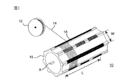
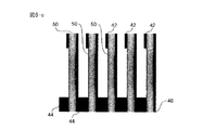
光ファイバーフェースプレートを製造するために適用される本発明を用いた特定の装置及び方法を理解するために、まず本発明の装置を用いて製造され且つ光ファイバーフェースプレートを組み立てるのに使用される基本的な構造構成単位を考察することが最も有益である。図12は、リボン構造体40の一部分を示す。リボン構造体40は、光ファイバーフェースプレート製造用の新規な基本的構成要素としての役割を果たす。リボン構造体40では、光ファイバーセグメント50を一般的に互いに平行に配置して整列させて、光をインプットエッジ46から幅Wをわたってアウトプットエッジ48に導くようにしている。インプットエッジ46でのファイバーセグメント50は、インプットエッジファイバー間隔Iを有している。以下で説明するように、インプットエッジスペーサー42は、固定されたインプットエッジファイバー間隔Iを維持し、また積み重ねたときにリボン構造体40間のインプットエッジ距離も決定する。ファイバーセグメント50は、グループ分けしてファイバー群32を形成してもよい。このように配置した状態で、インプットエッジ46でのファイバー群32間のインプットエッジファイバー群距離がIgとなる。同様に、アウトプットエッジ48でのファイバーセグメント50のアウトプットエッジファイバー間隔は、Oである。以下で説明するように、アウトプットエッジスペーサー44は、固定されたアウトプットエッジファイバー間隔Oを維持し、また互いに積み重ねたときに連続するリボン構造体40間のアウトプットエッジ距離も決定する。
To understand the specific apparatus and method using the present invention applied to manufacture a fiber optic faceplate, first the basic elements manufactured using the apparatus of the invention and used to assemble the fiber optic faceplate will be described. It is most useful to consider the various structural units. FIG. 12 shows a part of the
図1は、光ファイバーフェースプレート形成装置10及びリボン構造体40の製造の第一段階に使用される構成要素の斜視図である。光ファイバーフェースプレート形成装置10は、光ファイバー源12を備えている。光ファイバー源12を用いて光ファイバーストランド14を形成し、この光ファイバーストランド14を、マンドレル16に巻き取る。図1に示される構成要素は、互いに働き合って、マンドレル16のまわりに一般的にらせん形態に光ファイバーストランド14を巻き取る。この場合、マンドレルは、軸Aを中心として回転して、単一ファイバーストランド14の厚さの巻き取りらせん状物18を形成する。すなわち、巻き取りらせん状物18が、ある所定の長さLまで、マンドレル16の周囲に形成される。再び図12において、形成される各リボン構造体40は、図1に示すように、幅W及び長さLを有している。
FIG. 1 is a perspective view of components used in a first stage of manufacturing the optical fiber
図2により明瞭に示されているように、マンドレル16は、一つ以上のリボン形成チャンネル20を有している。各リボン形成チャンネル20は、一対のスペーシングガイド(インプットスペーシングガイド22とアウトプットスペーシングガイド24)により規定されている。幅Wのリボン構造体40を形成するために、インプットスペーシングガイド22及びアウトプットスペーシングガイド24が、約Wの距離離れている。図1及び図2の配置において、以下で説明する理由で特に好ましい実施態様である隣接するリボン形成チャンネル20におけるインプットスペーシングガイド22自体が、隣接している。同様に、隣接するリボン形成チャンネル20におけるアウトプットスペーシングガイド24が、隣接している。これらの場合、切断溝34が、隣接するインプットスペーシングガイド22間と隣接アウトプットスペーシングガイド24間とに設けられていて、リボン構造体40を互いに分離するようにしている。しかしながら、他の配置も可能である。
As shown more clearly in FIG. 2, the
マンドレル16の円周方向のリボン形成チャンネル20は、全て同じ幅Wの寸法を有していてよい。しかしながら、インプットスペーシングガイド22とアウトプットスペーシングガイド24の相対位置を変更することにより幅W寸法を増加させることが有利なことがある。インプットスペーシングガイド22及びアウトプットスペーシングガイド24は、マンドレル16上の所定の位置固定してもよいし、又は調整可能に、例えば、機械的若しくは磁気的に固定してもよい。光ファイバー源12は、機械技術分野において周知の機械的巻き取り法を用いて、光ファイバーストランド14をインプットスペーシングガイド22及びアウトプットスペーシングガイド24に巻きながら、軸Aの方向にそって移動することが好ましい。
The circumferential
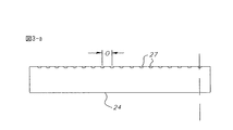
図3−a及び図3−bは、それぞれインプットスペーシングガイド22及びアウトプットスペーシングガイド24の小セグメントの拡大横断面を示す。溝27により、リボン構造体40のアウトプットエッジのファイバーをアウトプットファイバー間隔Oを有するように位置させる。溝27と同様に間隔をおいて配置した開口部を有する溝26は、それらの底面でのインプットエッジファイバー間隔IがOよりも小さくなるように変更可能に角度がつけられている。インプットファイバー間隔とアウトプットファイバー間隔が同じである光ファイバーフェースプレートを作製するためには、インプットスペーシングガイドとアウトプットスペーシングガイドの両方が同一である。好ましい実施態様によれば、機械加工溝が使用されるが、ピン機構を用いる等の交互配置を用いることができる。ただしこの場合、インプットエッジファイバー間隔I又はアウトプットエッジファイバー間隔Oを、正しく維持することが必要である。どのようにリボン構造体40を使用して光ファイバーフェースプレートを製造するのかによって、インプットスペーシングガイド22及びアウトプットスペーシングガイド24は、異なる寸法を有していてもよいし、又はそれらの間隔がマンドレル16の異なる部分で異なっていてもよい。任意の切断溝34を、図示したように、隣接して配置されたインプットスペーシングガイド22間又は隣接して配置されたアウトプットスペーシングガイド24間に設けることができる。
FIGS. 3-a and 3-b show enlarged cross-sections of small segments of the
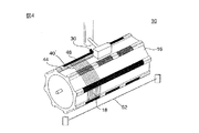
図4は、リボン構造体40の製造の第二段階に使用される光ファイバーフェースプレート形成装置10及び構成要素の斜視図である。一旦巻き取られたらせん状物18をマンドレル16に巻き取ると、図1に示す製造の第一段階で設けた相対的インプットエッジファイバー間隔Iとアウトプットエッジファイバー間隔Oを固定することが必要となる。このために、エッジスペーサーアプリケータ30により、アウトプットエッジスペーサー44を、部分的に作製されたリボン構造体40’のアウトプットエッジ48に沿って巻き取られたらせん状物18の上に適用する。好ましい実施態様によれば、アウトプットエッジスペーサー44は、接着性裏当てを備えていて、接着テープと同様な方法で適用できる。
FIG. 4 is a perspective view of the optical fiber
ここで、インプットエッジスペーサー42及びアウトプットエッジスペーサー44を適用するには、多数の別法を使用することができる。例えば、接着剤がそれ自体マンドレル16構成要素に付着しない場合には、接着剤を巻き取りらせん状物18に直接適用するのが好ましいことがある。他の固定方法では、例えば、熱硬化性プラスチックを用いたインプットエッジスペーサー42又はアウトプットエッジスペーサー44に熱を加えてもよい。インプットエッジスペーサー42又はアウトプットエッジスペーサー44を適用する順序も、例えば、リボン構造体40を積み重ねる順序に応じて変更してもよい。したがって、インプットエッジスペーサー42又はアウトプットエッジスペーサー44を、交互するリボン形成チャンネル20について、異なる時期に、1セットを巻き取りらせん状物18の形成前に適用し、もう1セットを巻き取りらせん状物18の形成後に適用することが最も適当なことがある。
Here, a number of alternatives can be used to apply the
一旦インプットエッジスペーサー42及びアウトプットエッジスペーサー44を適用すると、完成したリボン構造体40を、マンドレル16から取り除くことができる。リボン構造体40を、当該技術分野において周知の光ファイバーを切断するための多数の方法により互いに分離できる。図4の実施態様によれば、例えば、加熱したニクロム線52をマンドレル16に当てて、組み立てたリボン構造体40を分離する。例えば、以下で説明するように、組み立てたリボン構造体40を完全なシート又はスリーブとして分離する等の他の方法を使用してもよい。
Once the
インプットエッジスペーサー42及びアウトプットエッジスペーサー44は、多数の異なる材料から製造でき、例えば、テープ、プラスチック、接着剤でもよいし、成形してもよい。
The
図5〜図11は、上記したようにして製造されたリボン構造体40をどのように組み合わせて光ファイバーフェースプレートを構成するかを示している。図5は、各光ファイバーセグメント50並びにインプットエッジスペーサー42及びアウトプットエッジスペーサー44から構成されるリボン構造体40の小セグメントの斜視図である。
5 to 11 show how the
図6−a〜図6−dは、光ファイバーフェースプレートの製造の一部分として、どのようにリボン構造体40を互いに積み重ねるかを示す側面図である。図6−aは、単一のリボン構造体40を示す。図6−bは、インプットエッジスペーサー42とアウトプットエッジスペーサー44を積み重ねに適当な向きとして、複数のリボン構造体40を対称的に並べたものを示している。図6−cは、アウトプットエッジスペーサー44を光ファイバーセグメント50の間に配置して、どのようにしてアウトプットエッジ48を組み立てるかを示している。図6−dは、次にどのようにして点線で示したインプットエッジ46を形成するかを示している。図6−dで示すように、インプットエッジ46で多少のトリミングをおこなって平坦度を維持することが必要なことがある。
FIGS. 6A to 6D are side views illustrating how the
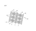
図7−a及び図7−bは、リボン構造体40を互いに積み重ねて光ファイバーフェースプレート100のアセンブリを形成する順序を示す斜視図である。図7−aにおいて、隣接するリボン構造体40を並べるために、一連の整列スロット36を設けている。図7−bに示すように、整列ピン38又は他の位置決め構造体を使用して、隣接するリボン構造体40の相対位置を固定することができる。
FIGS. 7A and 7B are perspective views illustrating the order in which the
図8は、本発明の方法により製造した光ファイバーフェースプレート100をセグメントのアウトプット面104からみた斜視図である。インプット側では、クラスター54が有用であり、これにより、一組のファイバーセグメント50がより小さな領域に一定の経路で延びている。この場合、上記したように、クラスター54間の間隙は、リボン構造体40内の距離Igにより規定される。図8に示すように、アウトプットエッジファイバー間隔Oは、典型的にはリボン構造体40内のファイバーセグメント50間及び隣接するリボン構造体40間と同じである。同様に、インプットエッジファイバー間隔Iは、少なくともクラスター54内では、直交方向において等しい。クラスター54間のインプットエッジファイバー群距離Igを、維持する。剛性の追加と支持のため、追加のスペーシング構造体を使用して、リボン構造体40内のインプットエッジファイバー群距離Igを維持できる。追加の直交支持構造体を使用することもできる。
FIG. 8 is a perspective view of the optical
図9は、本発明の方法により製造した光ファイバーフェースプレート100をセグメントのインプット面102からみた斜視図である。図9では、一つのクラスター54が点線ボックスで強調表示されている。
FIG. 9 is a perspective view of the
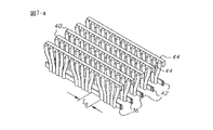
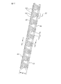
光ファイバーフェースプレート100を形成するために、リボン構造体40を、個々に切断し一緒に(一度に一つのリボン構造体40)積み重ねることができる。別法として、折り畳み法を使用して、光ファイバーフェースプレート100を形成できる。例えば、図13の斜視図に示す一つの実施態様によれば、長さが最終的に組み立てられたファイバーフェースプレート100の幅の寸法の数倍するように製造されたリボン構造体40を、折り目Fのところでそれ自体の上に一回以上折り返して、ファイバーフェースプレート100構造体列を構築する。
To form the
もう一つの別法では、シート系モデルに準じてファイバーフェースプレート100を構築する。図10は、マンドレル16上にアセンブリを完成することにより、4つの個々のリボン構造体40のセグメントを一枚のリボン構造体58として得たときの図である。ある時点で、リボン構造体を、インプットエッジ46とアウトプットエッジ48が整列するように分離線Sで分離する。図4に関して上記したように、この分離は、切断手段によるか、熱を用いておこなうことができ、リボン構造体40をマンドレル16で製造するときにおこなうことができる。しかしながら、図11−a及び図11−bに示すように、本発明の方法により、蛇腹状折り曲げ法を用いてリボン構造体40の新規な積み重ね法も実現できる。図11−aは、一枚のリボン構造体58上の複数のリボン構造体40を、蛇腹状折り曲げ形式で互いに折り曲げた場合の斜視図である。図11−bは、蛇腹状折り曲げ法の側面図である。この方法では、一枚のリボン構造体58を、各対の隣接するインプットエッジスペーサー42の間及び各対の隣接するアウトプットエッジスペーサー44の間で折り曲げる。それにより、図11−bに示すように、各リボン構造体40を整列して、インプットエッジ46とアウトプットエッジ48を形成する。
In another alternative, the
一旦リボン構造体40がインプット面102及びアウトプット面104を形成するように適切に整列させたら、仕上げ操作をおこなうことができる。これらのプロセスでは、最終付形がおこなわれ、材料をケースに入れ、表面仕上げ操作をおこなう。また、組み立てた光ファイバーフェースプレート100の光学性能を向上させる方法を用いることもできる。
Once the
仕上げ操作は、例えば、図11−bに示すように、リボン構造体40の間に残存するループ56を分離することが含まれる。図2に戻って、切断溝34は、蛇腹状折り曲げ法に適用するように追加の幅を設けて好適な寸法とすることができる。
Finishing operations include, for example, separating
光ファイバーセグメント50の端部を付形するのに、熱を用いてもよい。例えば、熱を加えて各光ファイバーセグメント50の端部を付形することにより、各ファイバーセグメント50ごとに一体レンズ構造を形成してもよい。別法として、熱と圧力を加えて、インプットエッジ46とアウトプットエッジ48の一方又は両方のファイバー直径を大きくしてもよい。
Heat may be used to shape the end of the
光ファイバーセグメント50間の空間を充填するのに使用する間隙物質の種類は、何種類でもよい。間隙材料には、プラスチック、樹脂、エポキシ樹脂又は他の好適な材料、例えば、光ガイド性等の特定の光学的性質について選択された材料等でよい。黒色の間隙材料又は特定の光学指数を有する間隙材料を用いて、ファイバーセグメント50間のクロストーク等の望ましくない影響を防止することができる。光ファイバーフェースプレートをある種の硬膜液に浸漬することにより、仕上げをおこなうことができる。
Any number of types of interstitial materials can be used to fill the space between the
ここで、ある用途では、可撓性光学フェースプレート配置が最も有利なことがあるので、間隙物質の使用は任意である。例えば、ある用途では、ディザリング又は他の機械的運動若しくは可撓性が有用なことがある。 Here, for some applications, the use of interstitial material is optional, as a flexible optical faceplate arrangement may be most advantageous. For example, dithering or other mechanical movement or flexibility may be useful in some applications.
仕上げ操作の一部分として、アウトプット面104にコーティングを適用してもよい。コーティングは、反射防止特性を付与するため、又はマウントに好適な表面を提供するために使用できる。追加の光学構成要素を、仕上げプロセスの一部分としてアウトプット面104に適用して使用することにより、好ましい光学効果を得ることができる。補助光学構成要素及びコーティングを使用して、例えば、アウトプット面104で円偏光等の偏光を得ることができる。
A coating may be applied to
光ファイバーフェースプレート製造に伴う一つの重要な問題に、アレイ又は「ピクセル対ピクセル」整列における個々の光源に対するファイバー配列がある。この問題は、上記した背景技術で説明した従来の製造方法を用いた高密度画像形成用途については、十分な解決がなされなかった。その代わり、ファイバーの少なくとも一部分が意図する光を受けるように一般的に単一光源について複数のファイバーをグルーピングする等のある種の次善策が使用された。しかしながら、このような解決策では、ピクセル対ピクセル整列が得られず、明らかに光ファイバーフェースプレート構造体の解像度が制約される。 One important issue with fiber optic faceplate fabrication is the fiber arrangement for individual light sources in an array or "pixel-to-pixel" alignment. This problem has not been sufficiently solved for high-density image forming applications using the conventional manufacturing method described in the background art above. Instead, certain workarounds have been used, such as grouping multiple fibers generally for a single light source such that at least a portion of the fibers receives the intended light. However, such a solution does not provide pixel-to-pixel alignment and obviously limits the resolution of the fiber optic faceplate structure.
本発明の方法を用いて、リボン構造体40の配置により、上記したように、インプットエッジスペーサー42及びアウトプットエッジスペーサー44を用いて、一列に配列された光源内及び列間で、ピクセル間隔を正しくすることができる。各列のリボン構造体40を互いに整列させることは、例えば、図7−a及び図7−bに示すような整列スロット36/整列ピン38配列法を用いる等の機械的方法によりおこなうことができる。他の使用することができる整列法には、インターロック部材を用いてインプットエッジスペーサー42及びアウトプットエッジスペーサー44を製造することが含まれる。ジグ又は他の機械的配列装置を用いて、一連の間隔を置いて配置したスロット又は他の物理的機構を利用してリボン構造体40セグメントを互いに整列させることができる。磁石を用いて、列同士の整列をおこなうことができる。この際、磁石構成要素又は鉄材料を利用したインプットエッジスペーサー42又はアウトプットエッジスペーサー44を用いる。
Using the method of the present invention, the arrangement of the
ディスプレイ用途及び印刷用途では、個々の光ファイバーセグメント50を対応するピクセルに合わせて整列させることが必要である。完成した光ファイバーフェースプレート100の配列を支持するため、その複合リボン構成要素40に、穴、窪み、ソケット、ピン等の機械的機構を備えることができる。別法として、磁石及び鉄構成要素を、複合リボン構造体40に内蔵させるか、複合リボン構造体40上に付加することができる。
For display and printing applications, it is necessary to align individual
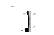
別の解決法を、図16に示す。この方法では、固有的にピクセル光源を光ファイバーセグメント50に対して整列させる。図16の整列では、OLED(有機発光ダイオード)等の発光ディスプレイ60を、光ファイバーフェースプレート100の表面114に対して直接作製する。これにより、個々のピクセル62を、光パイプとしての役割を果たす対応する光ファイバーセグメント50に対して直接形成できる。図16は、底面発光型OLEDについての可能な配置を示している。ピクセル62は、正確に配列されるように適所に直接配置することができる。同様に、上面発光型OLEDを、光ファイバーフェースプレート100の上部又は光ファイバーフェースプレート100に対して直接作製できる。
Another solution is shown in FIG. This method inherently aligns the pixel light source with the
発光ディスプレイ60は、例えば、OLED、PLED(ポリマー発光ダイオード)又はLEDアレイでよい。
The
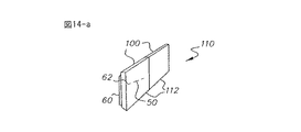
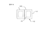
本発明の方法を用いて製造した光ファイバーフェースプレート100は、タイリング用途によく適している。図14−a及び図14−bは、タイリングにより張ったディスプレイ110を示す。このディスプレイ110は、複数タイル112の形態の複数発光表示装置60から画像を発生する。好ましい実施態様によれば、発光表示装置60は、OLEDである。各発光表示装置60により、画像の一つのタイル112が構成される。図14−bの平面図に示すように、光ファイバーフェースプレート100を使用して、発光表示装置60からの画像(図14−bに点線で示されている)のサイズを拡大することができる。図14−aで示されているように、各ファイバーセグメント50が、発光表示装置60の単一のピクセル62からの光を、画像タイル112の相当する位置に導くように、ピクセル対ピクセル整列を設けることができる。光ファイバーフェースプレート100を、例えば、機械的インターロック又は磁石を用いて互いに整列させることができる。隣接する画像タイル112におけるリボン構造体40を、それらの光ファイバーフェースプレート100のエッジからオフセットして、隣接する画像タイル112を結合するための方法として相互かみあいを可能とすることができる。
The
リボン構造体40を使用することにより、光ファイバーフェースプレート100の寸法及び曲率をかなり柔軟に適合させることができる。リボン構造体40セグメントの長さを変化させることにより、高さ及び幅について種々の設定が可能となる。リボン構造体40を、多数の異なる方法でラッピングして光ファイバーフェースプレート100の形状に適合させることができる。
By using the
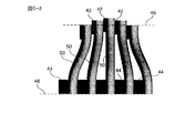
インプットエッジスペーサー42及びアウトプットエッジスペーサー44に対してわずかに適合させることにより、リボン構造体40を組み合わせてアウトプット面104に湾曲を付与することができる。図15において、リボン構造体40を、インプットエッジスペーサー42に多数のスリット64を設けて湾曲に適合させて、図示した湾曲を形成する。湾曲は、凸方向であっても、凹方向であってもよい。例えば、アウトプットエッジスペーサー44にレリーフカットを設けることによるか、又はアウトプットエッジ48をトリミングするか、輪郭をつけることにより、さらに高レベルの付形が可能となる。次に、湾曲化とタイリングとを組み合わせることにより、本発明の方法を用いて大きなディスプレイ構造体を組み立てることができる。
With a slight adaptation to the
本発明の製造方法を用いた光ファイバーフェースプレート100は、多数の代替実施態様が可能である。光ファイバーフェースプレート100は、テーパーフェースプレートであることができる。光ファイバーセグメント50は、典型的にはほとんどの用途において同じ公称幅を有するが、リボン構造体40が異なる半径寸法を有する光ファイバーセグメント50を使用する実施態様も可能である。また、リボン構造体40が異なる形状、例えば、非円形状を有する光ファイバーセグメント50を含む実施態様も可能である。図11−bにおいて、補助スペーサー66を、いずれかの積み重ね配置でリボン構造体40間に付加することができる。はめ込み式補助スペーサー66を、インプットエッジ46又はアウトプットエッジ48に、例えば、光ファイバーセグメント50への接着性を向上させるために用いることができる。
Many alternative embodiments of the
ここで、本明細書において使用される用語「インプット」及び「アウトプット」は、相対的な用語であり、逆にすることができる。これらの用語をここで使用するのは、光ファイバーフェースプレート100を、例えば、タイル張り型ディスプレイを含むディスプレイの一部として使用することに関連する。光ファイバーフェースプレート100は、集光機器の一部として使用することができる。この場合、インプット側では、典型的には、光をアウトプット側の小さな検知構成要素に導くために、ファイバー間距離を大きくする必要がある。本発明の方法によると、どちらの方向にも使用できる光ファイバーフェースプレート100を製造して、対向面での間隔が可変である、又は必要に応じて等間隔にした、そのような光変換器を提供することができる。
Here, the terms “input” and “output” as used herein are relative terms and can be reversed. The use of these terms herein relates to using
10…光ファイバーフェースプレート形成装置
12…光ファイバー源
14…光ファイバーストランド
16…マンドレル
18…巻き付けらせん状物
20…リボン形成チャンネル
22…インプットスペーシングガイド
24…アウトプットスペーシングガイド
26…溝
27…溝
30…エッジスペーサーアプリケータ
32…ファイバー群
34…切断溝
36…整列スリット
38…整列ピン
40…リボン構造体
40’…部分的に製造されたリボン構造体
42…インプットエッジスペーサー
44…アウトプットエッジスペーサー
46…インプットエッジ
48…アウトプットエッジ
50…光ファイバーセグメント
52…ニクロム線
54…クラスター
56…ループ
58…リボン構造体のシート
60…発光表示装置
62…ピクセル
64…スリット
66…補助スペーサー
100…光ファイバーフェースプレート
102…インプット面
104…アウトプット面
110…タイル張り型ディスプレイ
112…画像タイル
114…表面構造体
DESCRIPTION OF
Claims (1)
(b)該リボン構造体を上下に続けて積み重ね、該光パイプセグメントの列が隣接するスタックとして光変換器を構築することを特徴とする、光変換器の形成方法。 (A) each ribbon structure has a ribbon width defined by an input edge and an output edge, and has a row of parallel light pipe segments, each of the light pipe segments being at the input edge; Forming a plurality of ribbon structures providing an optical path from an inlet to an outlet at the output edge; and (b) stacking the ribbon structures one above the other, wherein the rows of light pipe segments are adjacent. A method of forming an optical converter, comprising: constructing an optical converter.
Applications Claiming Priority (1)
| Application Number | Priority Date | Filing Date | Title |
|---|---|---|---|
| US10/314,843 US7292760B2 (en) | 2002-12-09 | 2002-12-09 | Optical converter formed from flexible strips |
Publications (1)
| Publication Number | Publication Date |
|---|---|
| JP2004191982A true JP2004191982A (en) | 2004-07-08 |
Family
ID=32468578
Family Applications (1)
| Application Number | Title | Priority Date | Filing Date |
|---|---|---|---|
| JP2003409137A Pending JP2004191982A (en) | 2002-12-09 | 2003-12-08 | Method for forming optical converter |
Country Status (2)
| Country | Link |
|---|---|
| US (2) | US7292760B2 (en) |
| JP (1) | JP2004191982A (en) |
Families Citing this family (10)
| Publication number | Priority date | Publication date | Assignee | Title |
|---|---|---|---|---|
| US10593092B2 (en) * | 1990-12-07 | 2020-03-17 | Dennis J Solomon | Integrated 3D-D2 visual effects display |
| US7481777B2 (en) * | 2006-01-05 | 2009-01-27 | Roche Diagnostics Operations, Inc. | Lancet integrated test element tape dispenser |
| US7024082B2 (en) * | 2003-05-16 | 2006-04-04 | Eastman Kodak Company | Apparatus and method for forming an optical converter |
| US8308329B1 (en) * | 2009-12-18 | 2012-11-13 | Rockwell Collins, Inc. | Directionalizing fiber optic plate |
| US8294987B1 (en) * | 2011-09-09 | 2012-10-23 | Van Nuland Henricus Servatius Fransiscus | Image transforming device |
| US9274369B1 (en) * | 2012-10-30 | 2016-03-01 | Google Inc. | Seamless display with tapered fused fiber bundle overlay |
| US8977090B2 (en) | 2012-11-29 | 2015-03-10 | Delphi Technologies, Inc. | Contoured display |
| US9645303B2 (en) * | 2013-03-15 | 2017-05-09 | Cree, Inc. | Luminaires utilizing edge coupling |
| TW201506865A (en) * | 2013-08-09 | 2015-02-16 | jun-yi Lv | Optical fiber with image offset |
| CN108897095B (en) * | 2018-08-03 | 2023-05-26 | 华侨大学 | Directional backlight naked eye 3D parallel optical fiber array manufacturing device |
Family Cites Families (26)
| Publication number | Priority date | Publication date | Assignee | Title |
|---|---|---|---|---|
| US3033731A (en) | 1958-03-06 | 1962-05-08 | American Optical Corp | Method for the manufacture of optical image-transfer devices |
| US3141106A (en) * | 1958-12-12 | 1964-07-14 | American Optical Corp | Image transmitting screen |
| US3514351A (en) * | 1965-10-07 | 1970-05-26 | Nippon Glass Fiber Co Ltd | Method of obtaining an optical image transferable fiber bundle |
| US3741839A (en) * | 1968-11-07 | 1973-06-26 | Y Komiya | Method of manufacturing flexible optical fiber strand for transmitting images and apparatus therefor |
| US3607560A (en) * | 1969-05-15 | 1971-09-21 | American Optical Corp | Apparatus for making monofilament fiber optic ribbons for coherent fiberscopes |
| US3989578A (en) | 1971-07-14 | 1976-11-02 | Olympus Optical Co., Ltd. | Apparatus for manufacturing optical fiber bundle |
| JPS557564B2 (en) * | 1972-09-16 | 1980-02-26 | ||
| US4839635A (en) * | 1987-01-12 | 1989-06-13 | Inwave Corporation | Signboard for displaying optical images |
| FR2653926B1 (en) * | 1989-10-26 | 1994-04-29 | Commissariat Energie Atomique | METHOD FOR MANUFACTURING AN IMAGE ENLARGER MODULE FOR LIGHT PANELS WITH OPTICAL FIBERS. |
| US5009475A (en) * | 1989-12-27 | 1991-04-23 | Advance Display Technologies, Inc. | Image transfer device and method of manufacture |
| CA2084103C (en) * | 1991-12-02 | 1999-07-27 | Keiji Sakai | A display apparatus |
| US5204927A (en) | 1992-03-02 | 1993-04-20 | Polaroid Corporation | Method and apparatus for making a fiber optical coupler |
| US5376201A (en) | 1992-04-02 | 1994-12-27 | Kingstone; Brett M. | Method of manufacturing an image magnification device |
| US5313542A (en) | 1992-11-30 | 1994-05-17 | Breault Research Organization, Inc. | Apparatus and method of rapidly measuring hemispherical scattered or radiated light |
| JP2806737B2 (en) * | 1993-04-28 | 1998-09-30 | シャープ株式会社 | Display device |
| US5572034A (en) | 1994-08-08 | 1996-11-05 | University Of Massachusetts Medical Center | Fiber optic plates for generating seamless images |
| JP4012686B2 (en) * | 1998-02-05 | 2007-11-21 | 浜松ホトニクス株式会社 | Optical components |
| US5938812A (en) | 1998-05-14 | 1999-08-17 | Amorphous Materials, Inc. | Method for constructing a coherent imaging bundle |
| US6198872B1 (en) * | 1998-07-21 | 2001-03-06 | Hyla Lipson | Programmed fiberoptic illuminated display |
| EP0977063A1 (en) * | 1998-07-28 | 2000-02-02 | Interuniversitair Micro-Elektronica Centrum Vzw | A socket and a system for optoelectronic interconnection and a method of fabricating such socket and system |
| US6418254B1 (en) | 1999-06-04 | 2002-07-09 | Shizuki Electric Company, Inc. | Fiber-optic display |
| US6195016B1 (en) | 1999-08-27 | 2001-02-27 | Advance Display Technologies, Inc. | Fiber optic display system with enhanced light efficiency |
| US6304703B1 (en) | 2000-01-13 | 2001-10-16 | Transvision, Inc. | Tiled fiber optic display apparatus |
| JPWO2002013167A1 (en) * | 2000-08-03 | 2004-02-12 | 株式会社アクティブ・テック | Optical fiber positioning element of optical fiber focusing section in optical fiber type display device, method of manufacturing the same, and optical fiber type display device thereof |
| US6487351B1 (en) | 2000-11-06 | 2002-11-26 | Schott Fiber Optics | Fiber optic faceplate |
| US7149393B2 (en) * | 2002-12-09 | 2006-12-12 | Eastman Kodak Company | Apparatus and method for forming a fiber optic faceplate |
-
2002
- 2002-12-09 US US10/314,843 patent/US7292760B2/en not_active Expired - Fee Related
-
2003
- 2003-12-08 JP JP2003409137A patent/JP2004191982A/en active Pending
-
2007
- 2007-08-14 US US11/838,285 patent/US7892381B2/en not_active Expired - Fee Related
Also Published As
| Publication number | Publication date |
|---|---|
| US7892381B2 (en) | 2011-02-22 |
| US20070277922A1 (en) | 2007-12-06 |
| US20040108046A1 (en) | 2004-06-10 |
| US7292760B2 (en) | 2007-11-06 |
Similar Documents
| Publication | Publication Date | Title |
|---|---|---|
| US7892381B2 (en) | Method for forming an optical converter | |
| US7149393B2 (en) | Apparatus and method for forming a fiber optic faceplate | |
| US7548676B2 (en) | Apparatus and method for forming an optical converter | |
| US7228051B2 (en) | Light pipe with alignment structures | |
| US4116739A (en) | Method of forming an optical fiber device | |
| US4773730A (en) | Fiber optic light transfer devices and assemblies | |
| JP2020507128A5 (en) | ||
| US5376201A (en) | Method of manufacturing an image magnification device | |
| JPH0583881B2 (en) | ||
| WO1995001298A9 (en) | Method of manufacturing an image magnification device | |
| KR100602141B1 (en) | Fresnel lens sheet, method of producing the same, mold used for the production of the same, and projection screen including the fresnel lens sheet | |
| JP2001159726A (en) | Splitable optical fiber ribbon | |
| US7197218B2 (en) | Light pipe with molded optical surfaces | |
| JPH0766155B2 (en) | Method for producing printed matter with lens and printed matter with lens | |
| JP5699373B2 (en) | Manufacturing method of optical sheet | |
| JPS6133469A (en) | Lamination of optical fiber | |
| CN210005805U (en) | -dimensional integrated imaging double-vision 3D display device based on polarization grating | |
| JP2012058275A (en) | Method for manufacturing lens sheet, lens sheet, surface light source device and transmissive display device | |
| JP2007212779A (en) | Fiber pitch changing/separating tool | |
| JPH11149027A (en) | Production of optical tape cord | |
| JP2003149465A (en) | Light transmission body and its manufacturing method | |
| JPS61182001A (en) | Production of image guide | |
| JPH05203821A (en) | Optical fiber plate | |
| JP2004226940A (en) | Optical fiber array and method for manufacturing optical fiber array | |
| JPH03156490A (en) | Image display device for enlarging image |