JP2004178751A - Optical disk - Google Patents
Optical disk Download PDFInfo
- Publication number
- JP2004178751A JP2004178751A JP2002346134A JP2002346134A JP2004178751A JP 2004178751 A JP2004178751 A JP 2004178751A JP 2002346134 A JP2002346134 A JP 2002346134A JP 2002346134 A JP2002346134 A JP 2002346134A JP 2004178751 A JP2004178751 A JP 2004178751A
- Authority
- JP
- Japan
- Prior art keywords
- information signal
- substrate
- protective layer
- opening
- protrusion
- Prior art date
- Legal status (The legal status is an assumption and is not a legal conclusion. Google has not performed a legal analysis and makes no representation as to the accuracy of the status listed.)
- Abandoned
Links
Images

Abstract
Description
【0001】
【発明の属する技術分野】
この発明は、光ディスクに関し、特に、情報信号部を保護する保護層が設けられた側からレーザ光を照射することにより、情報信号の記録および/または再生が行われる光ディスクに適用して好適なものである。
【0002】
【従来の技術】
近年、光ディスクにおいては、さらなる高記録密度化が要求されている。そこで、基板に設けられた反射膜あるいは記録層上に、0.1mmの厚さを有する保護層を備えた次世代の高密度光ディスクが提案されている。この光ディスクでは、青紫色のレーザ光を、高NA(例えば、0.85)の対物レンズにより集光し、この集光したレーザ光を保護層側から反射膜あるいは記録層に照射することにより、情報信号の記録および/または再生が行われる。
【0003】
この次世代の高密度光ディスクの製造方法として、以下に示す方法が提案されている。
(1)厚みが制御された光透過性シート(例えば厚さ80μm)の片面に、感圧型粘着剤を均一に塗工(例えば厚さ20μm)したシートを作製し、このシートを円環状に打ち抜き、これを基板に重ね合わせて圧力をかけて接着する光ディスクの製造方法(以下、第1の光ディスクの製造方法と称する)。
(2)基板に設けられた反射膜あるいは記録層上にスピンコート法により紫外線硬化樹脂を塗布し、この紫外線硬化樹脂により基板に対し光透過性シートを貼り合わせる光ディスクの製造方法(以下、第2の光ディスクの製造方法と称する)。
【0004】
ところで、CD(Compact Disc)やDVD(Digital Versatile Disc またはDigital Video Disc)などの光ディスクでは、クランピング領域と反射膜あるいは記録層との間に、製造工程において光ディスクを重ねてストックした際に隣り合う光ディスク同士が接触することを防止するための突起が設けられている(例えば、特許文献1および2参照)。なお、この突起は、レーザ光が照射される側の面(以下、読み取り面と称する)に設けられている。反対面である印刷が施される面に突起を設けると、突起によって印刷ににじみが生じる、印刷の乗りが悪くなる、スクリーンが破れるなどの問題が生じるために、読み取り面側に突起が設けられている。
【0005】
【特許文献1】
特開平10−106044号公報
【0006】
【特許文献2】
特開2000−293902号公報
【0007】
そこで、このような突起を次世代の高密度光ディスクにも設けることが考えられている。ところが、この次世代の高密度光ディスクでは、CDやDVDなどの光ディスクとは異なり、保護層側ではなく基板側に印刷が施される。これは、上述したように、次世代の高密度光ディスクでは、保護層が形成された側からレーザ光を照射することにより情報信号の記録および/または再生が行われるためである。
【0008】
そこで、保護層が形成される側に突起が設けることが考えられる。この光ディスクの製造方法としては、上述の第2の光ディスクの製造方法を用いることが検討されている。ここで、第2の光ディスクの製造方法を用いるのは、第1の光ディスクの製造方法が以下のような問題を有するためである。
【0009】
(a)感圧型粘着剤を塗工した光透過性シートは、一般に100m以上の長さを持った巻物にて納品される。したがって、100m以上の長さに渡って厚みを制御することが要求されるが、このような長さで、光透過性シートの片面に、感圧型粘着剤を均一に塗工することは困難である。このため、感圧型粘着剤が均一に塗工された光透過性シートを製造するにはコストがかかり、光ディスクの製造コストの上昇を招いてしまう。
(b)光透過性シートを基板に対して貼り合わせる際に、光透過性シートと基板との間に気泡が混入してしまう。
【0010】
【発明が解決しようとする課題】
ところが、上述の第2の光ディスクの製造方法を用いて、CDやDVDなどの光ディスクにおけると同じように、クランピング領域と反射膜あるいは記録層との間に突起が設けられた次世代の高密度光ディスクを製造すると、以下のように、接着層の厚さが不均一になってしまうという問題が生じる。
【0011】
a)突起より外周側に紫外線硬化樹脂を滴下した場合には、紫外線硬化樹脂の滴下位置から外周側へ所定距離の区間(例えば、10mmの区間)の接着層の厚さが不均一になる。
b)突起より内周側に紫外線硬化樹脂を滴下した場合には、突起によって放射状の塗りムラが接着層に発生してしまう。
【0012】
したがって、この発明の目的は、光ディスクを重ねてストックした際に隣り合う光ディスク同士が接触することを防止するための突起を有する次世代の高密度光ディスクにおいて、均一な保護層を有する光ディスクを提供することにある。
【0013】
【課題を解決するための手段】
上記課題を解決するために、本願第1の発明は、中央部に開口を有する基板の一主面に、
レーザ光を照射することにより情報信号を記録可能および/または再生可能に構成された情報信号部と、
情報信号部を少なくとも覆う保護層とが順次積層され、
保護層側からレーザ光を情報信号部に照射することにより情報信号の記録および/または再生が行われる光ディスクにおいて、
基板が、開口とクランピング領域との間に、開口を中心とする円環状の突起または、開口を中心とする円周上に3以上の突起を有し
保護層が、突起とクランピング領域との間に滴下された樹脂をスピンコート法により少なくとも情報信号部上に塗布し、塗布された樹脂により光透過性シートを基板に対して貼り合わせることにより形成されることを特徴とする光ディスクである。
【0014】
この発明によれば、基板が、開口とクランピング領域との間に、開口を中心とする円環状の突起または、開口を中心とする円周上に3以上の突起を有するため、突起とクランピング領域との間にシートを基板に貼り合わせるための樹脂を滴下することができる。
【0015】
本願第2の発明は、中央部に開口を有する基板の一主面に、
レーザ光を照射することにより情報信号を記録可能および/または再生可能に構成された情報信号部と、
情報信号部を少なくとも覆う保護層とが順次積層され、
保護層側からレーザ光を情報信号部に照射することにより情報信号の記録および/または再生が行われる光ディスクにおいて、
基板が、開口とクランピング領域との間に、開口を中心とする円環状の突起または、開口を中心とする円周上に3以上の突起を有し、
保護層が、突起とクランピング領域との間に滴下された樹脂をスピンコート法により少なくとも情報信号部上に塗布し、硬化することにより形成されることを特徴とする光ディスクである。
【0016】
この発明によれば、基板が、開口とクランピング領域との間に、開口を中心とする円環状の突起または、開口を中心とする円周上に3以上の突起を有するため、突起とクランピング領域との間に保護層を形成するための樹脂を滴下することができる。
【0017】
【発明の実施の形態】
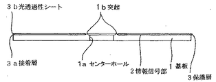
以下、この発明の一実施形態について図面を参照しながら説明する。図1に、この発明の一実施形態による光ディスクの構成の一例を示す。図1に示すように、光ディスクは、中央部にセンターホール1aが形成された円環形状を有する。そして、この光ディスクのレーザ光が照射される側の一主面には、センターホール1aを中心とする円環形状の突起1bが備えられている。この光ディスクのセンターホール1aの近傍には、光ディスクをスピンドルモータに装着するためのクランピング領域(図示を省略する)が設定されている。
【0018】
また、図1に示すように、この一実施形態による光ディスクは、基板1の一主面に、情報信号部2、保護層3を順次積層することにより構成される。なお、この一実施形態による光ディスクは、保護層3の側からレーザ光を情報信号部2に照射することにより、情報信号の記録および/あるいは再生が行われる光ディスク(例えば、Blu−ray Disc)である。
【0019】
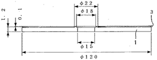
図2に、この発明の一実施形態による光ディスクの各部の大きさの一例を示す。光ディスクの径(直径)は、例えば120mmに選ばれる。光ディスクのセンターホール1aの径(直径)は、例えば15mmに選ばれる。光ディスクの厚さは、例えば、1.2mmに選ばれる。基板1の厚さは、例えば1.1mmに選ばれる。保護層3の厚さは、例えば0.1mmに選ばれる。突起1bの高さは、光ディスクのレーザ光が照射される側の面を基準として、0.05mm〜0.2mm、例えば0.1mmに選ばれる。クランピング領域は、例えば、直径23mm以上33mm以下で規定される領域である。
【0020】
基板1は、円環形状を有し、一主面には凹凸が形成されている。この基板1の材料としては、例えばポリカーボネート(PC)、アクリルあるいはポリオレフィンが用いられる。
【0021】
また、基板1の情報信号部2が形成される側の面には、センターホール1aを中心とする円環状の突起1bが形成されている。この突起1bは、光ディスクを積み重ねた場合に隣り合うディスク同士が接触することを防ぐためのものであり、センターホール1aとクランピング領域との間、例えば、直径15mm〜23mm、好適には、直径18mm〜22mmの領域に形成される。なお、突起1bの形状はこの例に限られるものではなく、センターホール1aを中心とする円周上に3以上の突起が形成されるようにしてもよい。
【0022】
情報信号部2は、保護層3を介してレーザ光を照射することにより情報信号を記録可能および/または再生するためのものである。具体的には、光ディスクが再生専用型である場合には、情報信号部2として金属からなる反射膜が選ばれ、光ディスクが追記型である場合には、有機色素材料からなる膜を少なくとも備えた記録層が選ばれ、書き換え可能型である場合には、光磁気材料からなる膜あるいは相変化材料からなる膜を少なくとも備えた記録層が選ばれる。
【0023】
保護層3は、接着層3a、光透過性シート3bを情報信号部2上に順次積層することにより構成される。接着層3aは、情報信号部2上に塗布された紫外線硬化樹脂を硬化することにより形成される。この接着層3aの厚さは、例えば20μmに選ばれる。なお、接着層3aの材料は、紫外線硬化樹脂に限定されるものではなく、紫外線硬化型以外の樹脂であってもかまわない。
【0024】
光透過性シート3bは、基板1におけると同様に、平面円環形状を有する。光透過性シート3bの材料としては、少なくとも情報信号の記録および/または再生に用いられるレーザ光を透過可能な光学特性を満足した材料が選ばれ、例えば、ポリカーボネートあるいはポリオレフィンが選ばれる。この光透過性シート3bの厚さは、例えば80μmに選ばれる。なお、この光透過性シート3bの厚さは、情報信号の記録および/または再生に用いられるレーザ光の波長や、保護層3の所望とする膜厚を考慮して決定される。
【0025】
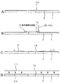
次に、図3を参照しながら、この発明の一実施形態による光ディスクの製造工程について説明する。まず、図3Aに示すように、一主面に凹凸が形成された基板1を射出成形により成形した後、凹凸が形成された一主面に情報信号部2を形成する。例えば、光ディスクが再生専用型である場合には、基板1の一主面にスパッタリングにより反射膜を成膜する。なお、突起1bは、例えば、射出成形装置(図示を省略する)により基板1を成形する際に形成される。具体的には、突起1bは、金型入れ子部に形成された溝によって形成される。なお、この金型入れ子部は、スタンパ取付側のスタンパ内径孔より内側に設けられている。
【0026】
次に、図3Bに示すように、突起1bとクランピング領域との間(例えば半径11mmの位置)に紫外線硬化樹脂が滴下されるように、ノズル10を移動させる。そして、基板1を回転するとともに、ノズル10から紫外線硬化樹脂11を滴下する。これにより、突起1bとクランピング領域との間に紫外線硬化樹脂11がセンターホール1aを中心とした円環状に塗布される。
【0027】
次に、図3Cに示すように、基板1を高速で回転する。これにより、突起1bとクランピング領域との間に塗布された紫外線硬化樹脂11が内周側から外周側に向かって広がり、情報信号部2上に紫外線硬化樹脂11が均一に塗布される。
【0028】
最後に、図3Dに示すように、情報信号部2上に均一に塗布された紫外線硬化樹脂11により、基板1に対して光透過性シート3bを貼り合わせ、紫外線を例えば光透過性シート3b側から紫外線硬化樹脂に対して照射する。これにより、基板1上に所望とする保護層3が形成される。
【0029】
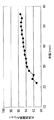
本発明者は、上述のようにして製造された一実施形態による光ディスクの保護層3の厚さと、従来の光ディスクの保護層の厚さとを測定し、その測定結果について比較検討を行った。ここで、一実施形態による光ディスクでは、接着層3aを形成するための紫外線硬化樹脂の滴下位置は、半径11mmの位置であり、従来の光ディスクでは、接着層を形成するための紫外線硬化樹脂の滴下位置は、半径20mmの位置である。
【0030】
図4に、従来の光ディスクの保護層の厚さの測定結果を示す。図5に、この発明の一実施形態による光ディスクによる保護層3の厚さの測定結果を示す。図4より、従来の光ディスクでは、滴下位置から外周側に向けて10mmの範囲では保護層の厚さが不均一になり、滴下位置から外周側に向けて20mm以上の領域では保護層の厚さが徐々に増加することが分かる。一方、図5より、この一実施形態による光ディスクでは、滴下位置から外周側に向けて5mm程度の範囲では保護層の厚さが単調に増加し、滴下位置から外周側に向けて5mm以上の領域では保護層の厚さがほぼ均一となることが分かる。
【0031】
この発明の一実施形態によれば以下の効果を得ることができる。
基板1が、センターホール1aとクランピング領域との間に、センターホール1aを中心とする円環状の突起1bを有するため、突起1bとクランピング領域との間に接着層3aとなる紫外線硬化樹脂を滴下することができる。よって、従来の光ディスクに比して情報信号部2上における保護層3の均一性を高めることができる。
【0032】
また、ストック後のポールからの搬送時における複数取りを防止することができる。また、光ディスクの読み取り面に突起1bが設けられているため、光ディスクを重ね合わせた際に隣り合う光ディスクが接触することを防止することができる。
【0033】
以上、この発明の一実施形態について具体的に説明したが、この発明は、上述の一実施形態に限定されるものではなく、この発明の技術的思想に基づく各種の変形が可能である。
【0034】
例えば、上述の一実施形態において挙げた数値はあくまでも例に過ぎず、必要に応じてこれと異なる数値を用いてもよい。
【0035】
また、紫外線硬化樹脂をスピンコート法により少なくとも情報信号部2上に塗布し、硬化することにより、保護層3を形成するようにした光ディスクに、この発明を適用してもよい。
【0036】
【発明の効果】
以上説明したように、この発明によれば、突起とクランピング領域との間にシートを基板に貼り合わせるための樹脂を滴下することができる。よって、従来の光ディスクに比して保護層の均一性を高めることができる。
【図面の簡単な説明】
【図1】この発明の一実施形態による光ディスクの構成の一例を示す断面図である。
【図2】この発明の一実施形態による光ディスクの各部の大きさの一例を示す断面図である。
【図3】この発明の一実施形態による光ディスクの製造工程を示す断面図である。
【図4】この発明の一実施形態による光ディスクの保護層の膜厚の測定結果を示すグラフである。
【図5】従来の光ディスクの保護層の膜厚の測定結果を示すグラフである。
【符号の説明】
1・・・基板、1a・・・センターホール、1b・・・突起、2・・・情報信号部、3・・・保護層、3a・・・接着層、3b・・・光透過性シート、10・・・ノズル、11・・・紫外線硬化樹脂[0001]
TECHNICAL FIELD OF THE INVENTION
The present invention relates to an optical disc, and more particularly to an optical disc suitable for application to an optical disc on which information signals are recorded and / or reproduced by irradiating a laser beam from a side provided with a protective layer for protecting an information signal portion. It is.
[0002]
[Prior art]
In recent years, optical disks have been required to have higher recording densities. Therefore, a next-generation high-density optical disk having a protective layer having a thickness of 0.1 mm on a reflective film or a recording layer provided on a substrate has been proposed. In this optical disc, blue-violet laser light is condensed by an objective lens having a high NA (for example, 0.85), and the condensed laser light is irradiated from the protective layer side to a reflective film or a recording layer. Recording and / or reproduction of the information signal is performed.
[0003]
The following method has been proposed as a method for manufacturing this next-generation high-density optical disk.
(1) A sheet in which a pressure-sensitive adhesive is uniformly applied (for example, 20 μm in thickness) to one surface of a light-transmitting sheet (for example, 80 μm in thickness) having a controlled thickness is produced, and this sheet is punched into an annular shape. And a method of manufacturing an optical disk in which the substrate is superimposed on a substrate and bonded by applying pressure (hereinafter, referred to as a first optical disk manufacturing method).
(2) A method for manufacturing an optical disk in which an ultraviolet-curable resin is applied by spin coating on a reflective film or a recording layer provided on a substrate, and a light-transmitting sheet is attached to the substrate with the ultraviolet-curable resin (hereinafter referred to as a second optical disk). This is referred to as an optical disk manufacturing method).
[0004]
Meanwhile, in an optical disc such as a CD (Compact Disc) or a DVD (Digital Versatile Disc or Digital Video Disc), the optical discs are adjacent to each other between the clamping area and the reflective film or the recording layer when the optical discs are stacked and stocked in the manufacturing process. Protrusions are provided to prevent the optical disks from contacting each other (for example, see
[0005]
[Patent Document 1]
JP-A-10-106044
[Patent Document 2]
JP 2000-293902 A
Therefore, it has been considered to provide such projections on next-generation high-density optical disks. However, in the next-generation high-density optical disk, unlike an optical disk such as a CD or a DVD, printing is performed on the substrate side instead of the protective layer side. This is because, as described above, in the next-generation high-density optical disk, recording and / or reproduction of an information signal is performed by irradiating a laser beam from the side on which the protective layer is formed.
[0008]
Therefore, it is conceivable that a projection is provided on the side on which the protective layer is formed. As a method of manufacturing the optical disk, use of the above-described method of manufacturing the second optical disk has been studied. Here, the second optical disk manufacturing method is used because the first optical disk manufacturing method has the following problems.
[0009]
(A) A light-transmitting sheet coated with a pressure-sensitive adhesive is generally delivered as a roll having a length of 100 m or more. Therefore, it is required to control the thickness over a length of 100 m or more, but it is difficult to uniformly apply a pressure-sensitive adhesive to one surface of the light-transmitting sheet with such a length. is there. For this reason, it is costly to manufacture a light-transmitting sheet on which a pressure-sensitive adhesive is uniformly applied, which leads to an increase in the manufacturing cost of an optical disk.
(B) When bonding the light transmissive sheet to the substrate, bubbles are mixed between the light transmissive sheet and the substrate.
[0010]
[Problems to be solved by the invention]
However, using the above-described second optical disc manufacturing method, a next-generation high-density optical disc in which protrusions are provided between a clamping area and a reflective film or a recording layer, as in an optical disc such as a CD or a DVD. When an optical disc is manufactured, there is a problem that the thickness of the adhesive layer becomes uneven as described below.
[0011]
a) When the ultraviolet curable resin is dropped on the outer peripheral side from the protrusion, the thickness of the adhesive layer in a section (for example, a section of 10 mm) at a predetermined distance from the drop position of the ultraviolet curable resin to the outer peripheral side becomes uneven.
b) When the ultraviolet curable resin is dropped on the inner peripheral side from the protrusion, radial uneven coating is generated on the adhesive layer by the protrusion.
[0012]
Therefore, an object of the present invention is to provide an optical disc having a uniform protective layer in a next-generation high-density optical disc having a projection for preventing adjacent optical discs from contacting each other when optical discs are stacked and stocked. It is in.
[0013]
[Means for Solving the Problems]
In order to solve the above-mentioned problems, the first invention of the present application discloses a method in which one main surface of a substrate having an opening in a central portion includes:
An information signal unit configured to be able to record and / or reproduce an information signal by irradiating a laser beam;
A protective layer covering at least the information signal portion is sequentially laminated,
In an optical disc on which information signals are recorded and / or reproduced by irradiating a laser beam to the information signal portion from the protective layer side,
The substrate has, between the opening and the clamping region, an annular protrusion centered on the opening or three or more protrusions on the circumference centered on the opening, and the protective layer has the protrusion and the clamping region. An optical disc characterized by being formed by applying at least an information signal portion with a resin dropped during the spin coating method, and bonding a light transmitting sheet to a substrate with the applied resin. .
[0014]
According to the present invention, since the substrate has between the opening and the clamping region an annular projection centering on the opening or three or more projections on a circumference centering on the opening, the projection and the clamping are provided. A resin for attaching the sheet to the substrate can be dropped between the ping region and the ping region.
[0015]
The second invention of the present application is directed to one principal surface of a substrate having an opening in a central portion,
An information signal unit configured to be able to record and / or reproduce an information signal by irradiating a laser beam;
A protective layer covering at least the information signal portion is sequentially laminated,
In an optical disc on which information signals are recorded and / or reproduced by irradiating a laser beam to the information signal portion from the protective layer side,
The substrate has, between the opening and the clamping region, an annular projection centering on the opening or three or more projections on a circumference centering on the opening,
An optical disc, wherein the protective layer is formed by applying a resin dropped between the protrusion and the clamping region on at least the information signal portion by a spin coating method and curing the resin.
[0016]
According to the present invention, since the substrate has between the opening and the clamping region an annular projection centering on the opening or three or more projections on a circumference centering on the opening, the projection and the clamping are provided. A resin for forming a protective layer between the ping region and the ping region can be dropped.
[0017]
BEST MODE FOR CARRYING OUT THE INVENTION
Hereinafter, an embodiment of the present invention will be described with reference to the drawings. FIG. 1 shows an example of the configuration of an optical disk according to an embodiment of the present invention. As shown in FIG. 1, the optical disc has an annular shape in which a center hole 1a is formed in the center. An
[0018]
Further, as shown in FIG. 1, the optical disc according to the embodiment is configured by sequentially laminating an
[0019]
FIG. 2 shows an example of the size of each part of the optical disc according to the embodiment of the present invention. The diameter (diameter) of the optical disk is selected to be, for example, 120 mm. The diameter (diameter) of the center hole 1a of the optical disc is selected to be, for example, 15 mm. The thickness of the optical disk is selected to be, for example, 1.2 mm. The thickness of the
[0020]
The
[0021]
An
[0022]
The
[0023]
The
[0024]
The light transmissive sheet 3b has a planar annular shape as in the
[0025]
Next, a manufacturing process of the optical disc according to the embodiment of the present invention will be described with reference to FIG. First, as shown in FIG. 3A, after a
[0026]
Next, as shown in FIG. 3B, the
[0027]
Next, as shown in FIG. 3C, the
[0028]
Finally, as shown in FIG. 3D, the light-transmitting sheet 3b is bonded to the
[0029]
The inventor measured the thickness of the
[0030]
FIG. 4 shows the measurement results of the thickness of the protective layer of the conventional optical disk. FIG. 5 shows a measurement result of the thickness of the
[0031]
According to the embodiment of the present invention, the following effects can be obtained.
Since the
[0032]
In addition, it is possible to prevent a plurality of pieces from being taken out from the pole after stocking. Further, since the
[0033]
As described above, one embodiment of the present invention has been specifically described. However, the present invention is not limited to the above-described embodiment, and various modifications based on the technical idea of the present invention are possible.
[0034]
For example, the numerical values given in the above-described embodiment are merely examples, and different numerical values may be used as needed.
[0035]
Further, the present invention may be applied to an optical disk in which a
[0036]
【The invention's effect】
As described above, according to the present invention, the resin for bonding the sheet to the substrate can be dropped between the protrusion and the clamping area. Therefore, the uniformity of the protective layer can be improved as compared with the conventional optical disc.
[Brief description of the drawings]
FIG. 1 is a sectional view showing an example of a configuration of an optical disc according to an embodiment of the present invention.
FIG. 2 is a sectional view showing an example of the size of each part of the optical disc according to one embodiment of the present invention.
FIG. 3 is a sectional view showing a manufacturing process of the optical disc according to the embodiment of the present invention.
FIG. 4 is a graph showing a measurement result of a film thickness of a protective layer of the optical disc according to the embodiment of the present invention.
FIG. 5 is a graph showing a measurement result of a thickness of a protective layer of a conventional optical disc.
[Explanation of symbols]
DESCRIPTION OF
Claims (4)
レーザ光を照射することにより情報信号を記録可能および/または再生可能に構成された情報信号部と、
上記情報信号部を少なくとも覆う保護層とが順次積層され、
上記保護層側からレーザ光を上記情報信号部に照射することにより情報信号の記録および/または再生が行われる光ディスクにおいて、
基板が、開口とクランピング領域との間に、上記開口を中心とする円環状の突起または、上記開口を中心とする円周上に3以上の突起を有し
保護層が、上記突起と上記クランピング領域との間に滴下された樹脂をスピンコート法により少なくとも情報信号部上に塗布し、塗布された上記樹脂により光透過性シートを上記基板に対して貼り合わせることにより形成されることを特徴とする光ディスク。On one main surface of the substrate having an opening in the center,
An information signal unit configured to be able to record and / or reproduce an information signal by irradiating a laser beam;
A protection layer covering at least the information signal portion is sequentially laminated,
An optical disc in which recording and / or reproduction of an information signal is performed by irradiating the information signal portion with a laser beam from the protective layer side,
The substrate has, between the opening and the clamping region, an annular protrusion centered on the opening or three or more protrusions on a circumference centered on the opening, and the protective layer has the protrusion and the protrusion. It is formed by applying a resin dropped between the clamping area and at least the information signal portion by a spin coating method, and bonding a light transmitting sheet to the substrate with the applied resin. An optical disc characterized by the following.
レーザ光を照射することにより情報信号を記録可能および/または再生可能に構成された情報信号部と、
上記情報信号部を少なくとも覆う保護層とが順次積層され、
上記保護層側からレーザ光を上記情報信号部に照射することにより情報信号の記録および/または再生が行われる光ディスクにおいて、
基板が、開口とクランピング領域との間に、上記開口を中心とする円環状の突起または、上記開口を中心とする円周上に3以上の突起を有し、
保護層が、上記突起と上記クランピング領域との間に滴下された樹脂をスピンコート法により少なくとも情報信号部上に塗布し、硬化することにより形成されることを特徴とする光ディスク。On one main surface of the substrate having an opening in the center,
An information signal unit configured to be able to record and / or reproduce an information signal by irradiating a laser beam;
A protection layer covering at least the information signal portion is sequentially laminated,
An optical disc in which recording and / or reproduction of an information signal is performed by irradiating the information signal portion with a laser beam from the protective layer side,
The substrate has between the opening and the clamping region an annular projection centering on the opening or three or more projections on a circumference centering on the opening,
An optical disc, wherein the protective layer is formed by applying a resin dropped between the protrusion and the clamping region on at least the information signal portion by a spin coating method and curing the resin.
Priority Applications (1)
| Application Number | Priority Date | Filing Date | Title |
|---|---|---|---|
| JP2002346134A JP2004178751A (en) | 2002-11-28 | 2002-11-28 | Optical disk |
Applications Claiming Priority (1)
| Application Number | Priority Date | Filing Date | Title |
|---|---|---|---|
| JP2002346134A JP2004178751A (en) | 2002-11-28 | 2002-11-28 | Optical disk |
Publications (1)
| Publication Number | Publication Date |
|---|---|
| JP2004178751A true JP2004178751A (en) | 2004-06-24 |
Family
ID=32707133
Family Applications (1)
| Application Number | Title | Priority Date | Filing Date |
|---|---|---|---|
| JP2002346134A Abandoned JP2004178751A (en) | 2002-11-28 | 2002-11-28 | Optical disk |
Country Status (1)
| Country | Link |
|---|---|
| JP (1) | JP2004178751A (en) |
-
2002
- 2002-11-28 JP JP2002346134A patent/JP2004178751A/en not_active Abandoned
Similar Documents
| Publication | Publication Date | Title |
|---|---|---|
| JP4338688B2 (en) | Manufacturing method of optical information recording medium | |
| JPWO2002037483A1 (en) | Optical recording medium, optical recording medium manufacturing method, optical recording medium manufacturing apparatus, program, and medium | |
| JP2001209980A (en) | Method and device for production of optical information recording medium | |
| US7161893B2 (en) | Stamper for fabrication of optical recording medium, method of forming information recording area and light transmissive layer, and optical recording medium | |
| JP4258037B2 (en) | Optical recording medium and optical recording / reproducing apparatus using the same | |
| JP2002170279A (en) | Optical recording medium, its manufacturing method and injection molding machine | |
| JP2002008269A (en) | Optical recording medium and method for manufacturing the same | |
| JPH10283683A (en) | Optical recording medium and its manufacture | |
| US7221640B2 (en) | Method of manufacturing an optical storage medium and optical storage medium | |
| WO2005018901A1 (en) | Mold, substrate for optical disk, and optical disk | |
| CN100358032C (en) | Method of manufacturing an optical data storage medium, optical data storage medium and apparatus for performing said method | |
| JPH1173691A (en) | Production of optical disk and optical disk produced by that method | |
| JP3695109B2 (en) | Optical recording medium manufacturing apparatus | |
| JP4618111B2 (en) | Optical recording medium and manufacturing method thereof | |
| JP2000298879A (en) | Optical recording medium | |
| JP4258096B2 (en) | Optical recording medium manufacturing apparatus and manufacturing method | |
| JP2004178751A (en) | Optical disk | |
| WO2006028051A1 (en) | Method for producing optical information recording medium and optical information recording medium | |
| JP4284888B2 (en) | Optical information recording medium | |
| JP4306093B2 (en) | Optical recording medium, method for manufacturing the same, and injection molding apparatus | |
| KR100922428B1 (en) | Apparatus for attaching and detaching cap for optical disc spin-coating, apparatus for optical disc spin-coating using the same and method for preparing an optical disc using the same | |
| JP2007265515A (en) | Optical recording medium and its manufacturing method | |
| JP2003242680A (en) | Disk-shaped optical recording medium | |
| KR20030052770A (en) | Method for coating of cover layer in reverse tracking type disk | |
| JP2003217195A (en) | Method for manufacturing optical recording medium and manufacturing apparatus thereof |
Legal Events
| Date | Code | Title | Description |
|---|---|---|---|
| A977 | Report on retrieval |
Free format text: JAPANESE INTERMEDIATE CODE: A971007 Effective date: 20050620 |
|
| A131 | Notification of reasons for refusal |
Free format text: JAPANESE INTERMEDIATE CODE: A131 Effective date: 20050628 |
|
| A762 | Written abandonment of application |
Free format text: JAPANESE INTERMEDIATE CODE: A762 Effective date: 20050811 |