JP2004177578A - Electronic module - Google Patents
Electronic module Download PDFInfo
- Publication number
- JP2004177578A JP2004177578A JP2002342347A JP2002342347A JP2004177578A JP 2004177578 A JP2004177578 A JP 2004177578A JP 2002342347 A JP2002342347 A JP 2002342347A JP 2002342347 A JP2002342347 A JP 2002342347A JP 2004177578 A JP2004177578 A JP 2004177578A
- Authority
- JP
- Japan
- Prior art keywords
- circuit board
- terminals
- drive circuit
- main surface
- board
- Prior art date
- Legal status (The legal status is an assumption and is not a legal conclusion. Google has not performed a legal analysis and makes no representation as to the accuracy of the status listed.)
- Pending
Links
Images


Abstract
Description
【0001】
【発明の属する技術分野】
本発明は電子モジュールに関し、特に、電子回路基板、駆動回路基板および配線基板の実装構造に関する。
【0002】
【従来の技術】
例えば表示装置にLSIドライバを実装する方法として、テープオートマチックボンディング(TAB)技術がある。具体的には、ポリイミドを基材とするフレキシブル基板の上にLSIドライバが実装されて構成されるTCPを、表示パネルおよびプリント基板に接続する方法である。プリント基板は例えば4層のエポキシ樹脂層からなる多層構造を有している。各エポキシ樹脂層の間には、薄い銅箔の層が形成されており、この銅箔層には回路がパターニングされている。銅箔層の回路は、プリント基板の片面に形成された電気信号入力用の端子と接続されている。上記プリント基板の入力端子は、異方性導電層を介してTCPと熱圧着される。
【0003】
近年、表示装置の高精細化(画素の微細化)が主流になっており、これに伴って、表示パネルおよびTCPの端子が狭ピッチ化されている。しかしながら、狭ピッチ化により、隣接する端子間で短絡したり、位置合わせが困難になるという問題が発生する。
【0004】
また、表示装置の高精細化に伴って、LSIドライバのサイズが大きくなり、TCPのサイズが大きくなっている。TCPのサイズが大きくなると、表示装置の外形サイズが大きくなるという問題がある。
【0005】
そこで、図6に示す表示装置が特許文献1に提案されている。
【0006】
図6は特許文献1に開示された液晶表示装置の部分模式図である。この液晶表示装置は、液晶パネル1の端子領域2に、LSIドライバ5を備えるTCP4aおよび4bが実装されている。隣接するTCP4aおよびTCP4bの形状は互いに異なっている。この液晶表示装置では、液晶パネル1に隣接して実装されるTCP4aおよび4bの入力端子6bが、プリント基板3上で千鳥状に配置されている。上記液晶表示装置では、TCPの入力端子のピッチをある程度広く設定することができる。
【0007】
また、図7に示す表示装置が特許文献2に提案されている。
【0008】
図7は特許文献2に開示されている液晶表示装置の部分模式図である。図7に示すように特許文献2の液晶表示装置は、液晶パネル1の端子領域2に、LSIドライバ5を備えるTCP4が実装されている。
【0009】
TCP4は、入力端子6および出力端子7が形成されている端部領域よりも中央付近が幅広になったビア樽形状を有している。従って、LSIドライバ5のサイズが増大しても、TCPの外形サイズの増大が抑制されている。また、隣接するTCPの重なり合う部分に折り曲げ部8が設けられている。従って、複数のTCPが近接して実装されても、TCPと、隣接するTCPのLSIドライバ5とが重ならないようにされている。
【0010】
【特許文献1】
特開平5−173166号公報(図1)
【特許文献2】
特開平9−90392号公報(図2)
【0011】
【発明が解決しようとする課題】
しかしながら、上述した従来の液晶表示装置では、表示装置の更なる高精細化が求められた場合に十分に対応することができない。また、上記では液晶表示装置を例に従来の表示装置における問題を説明したが、上述の問題は液晶表示装置に限られず、有機EL表示装置など他の表示装置においても問題になる。さらに、表示装置に限られず、様々な電子モジュールで高密度(狭ピッチ)化が求められた場合にも、同様の問題が生じる。
【0012】
本発明は上記の課題に鑑みてなされたものであり、高密度化に対応可能な、電気的接続の信頼性の高い電子モジュールを提供することを目的とする。
【0013】
【課題を解決するための手段】
本発明の電子モジュールは、複数の回路素子と、前記複数の回路素子のそれぞれに接続された複数の信号線とを主面に有し、かつ、前記複数の信号線のそれぞれに接続された複数の基板端子を有する電子回路基板と、それぞれが駆動回路を有し、互いに隣接して前記電子回路基板に実装された第1駆動回路基板および第2駆動回路基板と、前記第1駆動回路基板および前記第2駆動回路基板のそれぞれに所定の信号を供給するための配線基板とを備える電子モジュールであって、前記配線基板は、前記電子回路基板の前記主面と同じ方向を向く主面と、前記主面に対向する裏面とのそれぞれに複数の端子を有し、前記第1駆動回路基板は、前記配線基板の前記主面の前記複数の端子と電気的に接続されており、前記第2駆動回路基板は、前記配線基板の前記裏面の前記複数の端子と電気的に接続されており、これにより上記課題が解決される。
【0014】
前記複数の基板端子は前記電子回路基板の前記主面および前記主面に対向する裏面に形成されており、前記第1駆動回路基板および前記第2駆動回路基板は、それぞれの主面に複数の入力端子および複数の出力端子を有し、前記第1駆動回路基板の前記複数の入力端子および前記複数の出力端子は、それぞれ、前記配線基板の前記主面の前記複数の端子および前記電子回路基板の前記主面の前記複数の基板端子と電気的に接続されており、前記第2駆動回路基板の前記複数の入力端子および前記複数の出力端子は、それぞれ、前記配線基板の前記裏面の前記複数の端子および前記電子回路基板の前記裏面の前記複数の基板端子と電気的に接続されていることが好ましい。
【0015】
前記第1駆動回路基板の前記主面と、前記第2駆動回路基板の前記主面とは、互いに反対方向を向くように配置されていることが好ましい。
【0016】
前記電子回路基板の前記裏面に形成された前記複数の基板端子は、前記電子回路基板の前記主面から、前記主面と前記裏面との間に存在する端面を介して、前記裏面まで延設された前記複数の信号線と接続されていることが好ましい。
【0017】
前記配線基板は、前記第1駆動回路基板の前記複数の入力端子と接続される前記複数の端子を第1端子領域に備え、かつ、前記第2駆動回路基板の前記複数の入力端子と接続される前記複数の端子を第2端子領域に備えており、前記配線基板の前記主面の法線方向から見て、前記第1端子領域の少なくとも一部と前記第2端子領域の少なくとも一部とが互いに重畳していてもよい。
【0018】
前記第1駆動回路基板の前記複数の入力端子と前記配線基板の前記複数の端子との間、前記第2駆動回路基板の前記複数の入力端子と前記配線基板の前記複数の端子との間、前記第1駆動回路基板の前記複数の出力端子と前記電子回路基板の前記複数の基板端子との間、および前記第2駆動回路基板の前記複数の出力端子と前記電子回路基板の前記複数の基板端子との間に異方性導電層が配置されていてもよい。
【0019】
前記第1駆動回路基板および前記第2駆動回路基板は、実質的に同一であることが好ましい。
【0020】
前記配線基板はPWBであることが好ましい。
【0021】
上述した電子モジュールを用いて、液晶表示装置が好適に構成される。
【0022】
【発明の実施の形態】
以下では、アクティブマトリクス型の液晶表示装置に用いられる液晶モジュールを例に本発明の実施形態を説明するが、本発明は、有機EL表示装置またはイメージセンサなどの電子機器に用いられる電子モジュールに広く適用することができる。
【0023】
本実施形態の液晶モジュールは、アクティブマトリクス基板(電子回路基板)と、アクティブマトリクス基板に実装された駆動回路基板と、駆動回路基板に所定の信号を供給するための配線基板とを備えている。アクティブマトリクス基板の主面には、スイッチング素子(回路素子)および、スイッチング素子に接続された信号線が設けられている。アクティブマトリクス基板にはさらに、信号線に接続された基板端子が設けられている。
【0024】
配線基板は、アクティブマトリクス基板の主面と同じ方向を向く主面と、この主面に対向する裏面とを有しており、主面および裏面のそれぞれに端子が設けられている。駆動回路基板(第1の駆動回路基板)は、配線基板の主面の端子と電気的に接続されており、上記駆動回路基板に隣接してアクティブマトリクス基板に実装されている他の駆動回路基板(第2の駆動回路基板)は、配線基板の裏面の端子と電気的に接続されている。
【0025】
上述の液晶モジュールでは、駆動回路基板との電気的接続のために配線基板に設けられる端子が、配線基板の主面および裏面のそれぞれに配置されている。従って、配線基板の主面のみに一列に端子を配置する場合に比べて、広いピッチで端子を配置することができるので、短絡を防止し、実装精度や歩留まり率を高くすることができる。よって、高精細化に対応可能な、電気的接続の信頼性の高い液晶モジュールが提供される。
【0026】
配線基板において、第1の駆動回路基板の入力端子と接続される端子が配線基板の第1端子領域に設けられており、第2の駆動回路基板の入力端子と接続される端子が配線基板の第2端子領域に設けられているとした場合、例えば、配線基板の主面の法線方向から見て、上記第1端子領域と第2端子領域とを部分的に重畳させて配置することができる。上記のように配線基板に端子領域を配置することにより、端子のピッチをより広くすることができる。
【0027】
なお、本明細書で「端子」とは、配線等と電気的に接続された部分であって、他の導電部材と電気的に接続可能な部分をいう。必ずしも配線等の端部に設けられている必要はなく、また、配線および端子が同一材料を用いて一体成型されていても、されていなくてもよい。
【0028】
ある実施形態では、アクティブマトリクス基板の主面と、この主面に対向する裏面との両方に基板端子が形成されている。上述したように配線基板およびアクティブマトリクス基板のそれぞれに端子および基板端子を設けた場合、第1および第2駆動回路基板に実質的に同一の駆動回路基板を用いることができるので、製造コストの増加を抑制できる。
【0029】
具体的には、実質的に同一の駆動回路基板で構成される第1および第2駆動回路基板を用いて以下のように実装される。
【0030】
第1および第2の駆動回路基板はいずれも、同一面(主面)に入力端子および出力端子を備えている。第1の駆動回路基板の入力端子を、配線基板の主面に形成された端子と電気的に接続し、かつ、出力端子を、アクティブマトリクス基板の主面に形成された基板端子と電気的に接続する。また、第2駆動回路基板の入力端子を、配線基板の裏面に形成された端子と電気的に接続し、かつ、出力端子を、アクティブマトリクス基板の裏面に形成された基板端子と電気的に接続する。第1および第2駆動回路基板は、それぞれの主面が互いに反対方向を向くように実装される。
【0031】
ある実施形態では、アクティブマトリクス基板の裏面に形成された基板端子は、アクティブマトリクス基板の主面から、主面と裏面との間に存在する端面を介して、裏面まで延設された信号線と接続されている。
【0032】
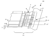
以下、図面を参照しながら本発明による実施形態の液晶モジュール100を説明する。図1は、液晶モジュール100の斜視図である。
【0033】
図1に示すように液晶モジュール100は、表示パネル2と、TCP(テープキャリアパッケージ)8と、プリント配線基板10とを備えている。表示パネル2は、アクティブマトリクス基板4と、基板4に対向して配置された対向基板6と、両基板の間に配置された液晶層(不図示)とを有している。液晶モジュール100では、駆動回路基板および配線基板としてそれぞれ、TCPおよびプリント配線基板(PWB)を用いる場合を例示するが、駆動回路基板および配線基板はこれらに限られない。例えば、駆動回路基板にCOF(チップオンフィルム)などを用いても良い。
【0034】
アクティブマトリクス基板4は、スイッチング素子として例えば画素を駆動するTFTを備え、信号線としてTFTに接続されるソース線およびゲート線を有している。ソース線およびゲート線はそれぞれ基板端子を備えており、これらの基板端子はTCPの出力端子と電気的に接続されている。対向基板6は液晶層側表面に対向電極(不図示)を備えている。TCP8は、プリント配線基板10に接続されている。プリント配線基板10は例えばFPC(不図示)に接続されており、FPCを介して外部回路基板から所定の信号等が供給されている。
【0035】
なお、以下の説明では、TFTおよび信号線が設けられているアクティブマトリクス基板4の面を表示パネル2またはアクティブマトリクス基板4の主面と称する場合がある。
【0036】
以下、液晶モジュール100を詳細に説明する。
【0037】
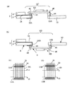
まず、図2および図3を参照しながらプリント配線基板10およびTCP8を説明する。図2(a)は、図1に示した液晶モジュール100の2A領域を示す部分平面図であり、図2(b)は図2(a)の液晶モジュール100を矢印2B方向から見た図である。なお、後述するが、図2は、図1に示したTCP8と異なる形状のTCP8を例示している。図3は、図2(a)に示すプリント配線基板10の3A―3A’に対応する断面図である。
【0038】
図2および図3に示すようにプリント配線基板10は、主面22および裏面24の両方に端子12を備えている。複数の端子12のうち、TCP8Aの入力端子と接続される端子12Aは、プリント配線基板10の主面22に形成されており、TCP8Aに隣接して実装されるTCP8Bの入力端子と接続される端子12Bは、プリント配線基板10の裏面24に形成されている。
【0039】
上記端子12のピッチは、プリント配線基板10の主面のみに端子を一列に配列して形成する場合に比べて広く設定されている。すなわち、主面22の法線方向からプリント配線基板10を見た場合に、端子12Aが設けられている端子領域と、端子12Bが設けられている端子領域とが部分的に重畳している。端子12Aと端子12bとは、それぞれ、プリント配線基板10の異なる面に設けられているので、上記のように配置されていても短絡することがない。
【0040】
図3に示すようにプリント配線基板10は、絶縁層(例えばエポキシ樹脂層)18の多層構造を有している。各絶縁層18の間および、主面22および裏面24には、所定の回路がパターンニングされた銅箔層20が形成されている。また、絶縁層18の所定の位置には、内部が導電材料で満たされたスルーホール16が設けられており、離間した銅箔層20は、スルーホール16によって電気的に接続されている。プリント配線基板10は上述した構成を備えており、主面22の端子12Aおよび裏面24の端子12Bから信号等を取り出すことができる。
【0041】
TCP8は、駆動回路(例えばドライバLSI)9と、プリント配線基板10の出力端子12と電気的に接続される入力端子(図2では不図示)と、液晶パネル2の基板端子(図2では不図示)と電気的に接続される出力端子(図2では不図示)とを備えている。入力端子および出力端子はTCP8の同一面(主面)に設けられており、駆動回路9は上記主面に対向する裏面に設けられている。液晶モジュール100に用いたTCP8はいずれも実質的に同一である。TCP8の入力端子のピッチは、上述したプリント配線基板10の端子12のピッチに対応して、従来よりも広く設定されている。
【0042】
複数のTCP8は、隣接するTCP8の主面が互いに反対方向を向くように実装されている。図2(a)に示すように例えば4つのTCP8は、矢印2Bの方向から順に、駆動回路9が設けられている面(裏面)が液晶モジュール100の表示面側(上側)、表示面の反対側(下側)、表示面側(上側)、および表示面の反対側(下側)を向くように実装されている。なお、図2(b)に示されている2つのTCP8のうち、駆動回路9が上側を向くように実装されているTCP8Aは、図2(a)の矢印2B方向から見て手前に存在しており、駆動回路9が下側を向くように実装されているTCP8Bは、矢印2B方向から見て上記TCP8Aの奥側に存在している。
【0043】
図2(a)に示す液晶モジュール100では、表示パネル2の主面の法線方向から見た場合に、隣接するTCP8同士が、端子領域だけでなく、端子領域以外で部分的に重畳し、重畳領域14が形成されるように実装されている。例えばTCP8に搭載される駆動回路9のサイズが大きくなり、TCP8の外形サイズが大きくなった場合、図1に示したように隣接するTCPの端子領域同士を部分的に重畳させるだけでなく、図2(a)に示すように重畳させた方が同数のTCP8をより狭い領域に実装できるので、表示装置の外形サイズの大型化を抑制できる。
【0044】
次に、図4を参照しながら、表示パネル2が備えるアクティブマトリクス基板4を説明する。
【0045】
図4は、図1に示したアクティブマトリクス基板4を矢印4A方向から見た図である。
【0046】
図4に示すように、アクティブマトリクス基板4は、主面38と、主面38と対向する裏面42と、主面38と裏面42との間に配置する端面40とを有している。信号線28は、端面40を介して裏面42まで延設されている。各信号線28は、例えば、主面38上に基板端子28Aを備え、裏面42上に基板端子28Bを備えており、主面38および裏面42の両方から信号等を取り出すことができるようになっている。
【0047】
信号線28および基板端子は例えば以下のようにして形成される。例えばAl(TaN)などの材料を用い、マスク蒸着によって信号配線28を形成する。信号線28を形成後、信号線28を覆うように絶縁膜を形成する。絶縁膜の所定の領域に開口部を形成し、信号線の所定の部分を露出させて、この部分を基板端子とする。
【0048】
なお、アクティブマトリクス基板4の主面38および裏面42の両方において、信号線28とTCP8の出力端子44とを電気的に接続することができれば、信号線および基板端子は上述した構成に限られない。例えば、信号線28のうち、所定の信号線のみが選択的に端面40を介して裏面42まで延設されていてもよい。
【0049】
図5(a)は図1に示した液晶モジュール100の5A―5A’に対応する断面図であり、図5(b)は5B―5B’に対応する断面図である。図5(c)は図5(a)の5C部分を表示パネル2の主面の法線方向から見た図を模式的に示している。図5(d)は図5(b)の5D部分を表示パネル2の主面の法線方向から見た図を模式的に示している。
【0050】
図5(a)および(c)に示すように、TCP8Aの出力端子48は、アクティブマトリクス基板4の主面42の基板端子28Aと接続されている。また、TCP8Aの入力端子46は、プリント配線基板10の主面の端子12Aと接続されている。また、図5(b)および(d)に示すように、TCP8Bの出力端子48は、アクティブマトリクス基板4の裏面38の基板端子28Bと接続されている。また、TCP8Bの入力端子46は、プリント配線基板10の裏面の端子12Bと接続されている。TCP8は、異方性導電層(ACF)44を挟んで表示パネル2および配線基板10に対して熱圧着されており、対応する端子間の電気的接続は上記ACF44を介して行われている。なお、図5(c)および(d)において、破線領域30は、ACF44によって熱圧着されている領域を示している。
【0051】
【発明の効果】
本発明により、高密度化に対応可能な、電気的接続の信頼性の高い電子モジュールを提供することができる。
【図面の簡単な説明】
【図1】本発明の実施の形態の概観模式図である。
【図2】(a)は、図1に示した液晶モジュールの2A領域を示す部分平面図であり、(b)は(a)の液晶モジュールを矢印2B方向から見た図である。
【図3】図2(a)に示すプリント配線基板の3A―3A’に対応する断面図である。
【図4】図1に示したアクティブマトリクス基板を矢印4A方向から見た図である。
【図5】(a)は図1に示した液晶モジュールの5A―5A’に対応する断面図であり、(b)は5B―5B’に対応する断面図であり、(c)は(a)の5C部分を表示パネルの主面の法線方向から見た図であり、(d)は(b)の5D部分を表示パネルの主面の法線方向から見た図である。
【図6】特許文献1に開示された液晶表示装置の部分模式図である。
【図7】特許文献2に開示された液晶表示装置の部分模式図である。
【符号の説明】
2 表示パネル
4 アクティブマトリクス基板
6 対向基板
8 TCP
8A TCP
8B TCP
9 駆動回路
10 プリント配線基板
12 端子
12A 端子
12B 端子
14 重畳領域
16 スルーホール
18 絶縁層
20 銅箔層
22 主面
24 裏面
28 信号線
28A 基板端子
28B 基板端子
38 主面
40 端面
42 裏面
44 出力端子
46 入力端子
48 出力端子[0001]
TECHNICAL FIELD OF THE INVENTION
The present invention relates to an electronic module, and more particularly, to a mounting structure of an electronic circuit board, a drive circuit board, and a wiring board.
[0002]
[Prior art]
For example, as a method of mounting an LSI driver on a display device, there is a tape automatic bonding (TAB) technology. Specifically, this is a method of connecting a TCP configured by mounting an LSI driver on a flexible substrate made of polyimide as a base material to a display panel and a printed circuit board. The printed board has a multilayer structure composed of, for example, four epoxy resin layers. A thin copper foil layer is formed between the epoxy resin layers, and a circuit is patterned on the copper foil layer. The circuit of the copper foil layer is connected to an electric signal input terminal formed on one side of the printed circuit board. The input terminal of the printed circuit board is thermocompression-bonded to TCP via an anisotropic conductive layer.
[0003]
2. Description of the Related Art In recent years, high definition (miniaturization of pixels) of a display device has become mainstream, and accordingly, the pitch of a display panel and terminals of a TCP have been narrowed. However, narrowing the pitch causes problems such as short-circuiting between adjacent terminals and difficulty in positioning.
[0004]
In addition, as the definition of the display device becomes higher, the size of the LSI driver increases, and the size of the TCP increases. When the size of the TCP increases, there is a problem that the outer size of the display device increases.
[0005]
Therefore, a display device shown in FIG. 6 is proposed in
[0006]
FIG. 6 is a partial schematic view of the liquid crystal display device disclosed in
[0007]
A display device shown in FIG. 7 is proposed in
[0008]
FIG. 7 is a partial schematic view of the liquid crystal display device disclosed in
[0009]
The TCP 4 has a via barrel shape in which the area near the center is wider than the end area where the input terminal 6 and the output terminal 7 are formed. Therefore, even if the size of the
[0010]
[Patent Document 1]
JP-A-5-173166 (FIG. 1)
[Patent Document 2]
JP-A-9-90392 (FIG. 2)
[0011]
[Problems to be solved by the invention]
However, the above-described conventional liquid crystal display device cannot sufficiently cope with a case where a higher definition of the display device is required. In the above description, the problem in the conventional display device is described by taking the liquid crystal display device as an example. However, the above problem is not limited to the liquid crystal display device, but also occurs in other display devices such as an organic EL display device. Further, the same problem occurs not only in the case of a display device but also in a case where high density (narrow pitch) is required in various electronic modules.
[0012]
The present invention has been made in view of the above problems, and an object of the present invention is to provide an electronic module with high electrical connection reliability that can cope with high density.
[0013]
[Means for Solving the Problems]
An electronic module according to an aspect of the invention includes a plurality of circuit elements and a plurality of signal lines connected to each of the plurality of circuit elements on a main surface, and a plurality of circuit elements connected to each of the plurality of signal lines. An electronic circuit board having a substrate terminal, a first drive circuit board and a second drive circuit board, each having a drive circuit, mounted on the electronic circuit board adjacent to each other, and the first drive circuit board and An electronic module comprising: a wiring board for supplying a predetermined signal to each of the second drive circuit boards, wherein the wiring board has a main surface facing the same direction as the main surface of the electronic circuit board; The first drive circuit board has a plurality of terminals on a back surface opposed to the main surface, and the first drive circuit board is electrically connected to the plurality of terminals on the main surface of the wiring board. The drive circuit board is Wherein said plurality of being electrically connected to a terminal of the back surface of the line board, thereby the problem is solved.
[0014]
The plurality of substrate terminals are formed on the main surface of the electronic circuit board and a back surface opposite to the main surface, and the first drive circuit board and the second drive circuit board have a plurality of An input terminal and a plurality of output terminals, wherein the plurality of input terminals and the plurality of output terminals of the first drive circuit board are respectively the plurality of terminals on the main surface of the wiring board and the electronic circuit board And the plurality of input terminals and the plurality of output terminals of the second drive circuit board are electrically connected to the plurality of substrate terminals of the second drive circuit board, respectively. And the plurality of board terminals on the back surface of the electronic circuit board.
[0015]
It is preferable that the main surface of the first drive circuit board and the main surface of the second drive circuit board are arranged so as to face in opposite directions.
[0016]
The plurality of substrate terminals formed on the back surface of the electronic circuit board extend from the main surface of the electronic circuit board to the back surface via an end surface existing between the main surface and the back surface. It is preferable to be connected to the plurality of signal lines.
[0017]
The wiring board includes the plurality of terminals connected to the plurality of input terminals of the first drive circuit board in a first terminal area, and is connected to the plurality of input terminals of the second drive circuit board. The plurality of terminals provided in a second terminal region, and at least a part of the first terminal region and at least a part of the second terminal region when viewed from a normal direction of the main surface of the wiring board. May overlap each other.
[0018]
Between the plurality of input terminals of the first drive circuit board and the plurality of terminals of the wiring board, between the plurality of input terminals of the second drive circuit board and the plurality of terminals of the wiring board, The plurality of output terminals of the first drive circuit board and the plurality of board terminals of the electronic circuit board, and the plurality of output terminals of the second drive circuit board and the plurality of boards of the electronic circuit board An anisotropic conductive layer may be arranged between the terminal and the terminal.
[0019]
Preferably, the first drive circuit board and the second drive circuit board are substantially the same.
[0020]
Preferably, the wiring board is made of PWB.
[0021]
A liquid crystal display device is suitably configured using the electronic module described above.
[0022]
BEST MODE FOR CARRYING OUT THE INVENTION
Hereinafter, embodiments of the present invention will be described by taking a liquid crystal module used for an active matrix type liquid crystal display device as an example. However, the present invention is widely applied to an electronic module used for an electronic device such as an organic EL display device or an image sensor. Can be applied.
[0023]
The liquid crystal module of the present embodiment includes an active matrix substrate (electronic circuit substrate), a driving circuit substrate mounted on the active matrix substrate, and a wiring substrate for supplying a predetermined signal to the driving circuit substrate. On the main surface of the active matrix substrate, switching elements (circuit elements) and signal lines connected to the switching elements are provided. The active matrix substrate is further provided with substrate terminals connected to the signal lines.
[0024]
The wiring substrate has a main surface facing in the same direction as the main surface of the active matrix substrate and a back surface facing the main surface, and terminals are provided on each of the main surface and the back surface. The drive circuit board (first drive circuit board) is electrically connected to the terminal on the main surface of the wiring board, and is another drive circuit board mounted on the active matrix substrate adjacent to the drive circuit board. The (second drive circuit board) is electrically connected to terminals on the back surface of the wiring board.
[0025]
In the above-described liquid crystal module, terminals provided on the wiring board for electrical connection with the drive circuit board are arranged on each of the main surface and the back surface of the wiring board. Therefore, the terminals can be arranged at a wider pitch than in a case where the terminals are arranged in a line only on the main surface of the wiring board, so that a short circuit can be prevented, and the mounting accuracy and the yield can be increased. Therefore, a liquid crystal module with high reliability of electrical connection that can cope with high definition is provided.
[0026]
In the wiring board, a terminal connected to the input terminal of the first drive circuit board is provided in a first terminal area of the wiring board, and a terminal connected to the input terminal of the second drive circuit board is provided on the wiring board. In the case where the second terminal region is provided in the second terminal region, for example, the first terminal region and the second terminal region may be partially overlapped with each other when viewed from the normal direction of the main surface of the wiring board. it can. By arranging the terminal regions on the wiring board as described above, the pitch of the terminals can be made wider.
[0027]
Note that, in this specification, a “terminal” is a portion that is electrically connected to a wiring or the like and is a portion that can be electrically connected to another conductive member. It is not necessary to be provided at the end of the wiring or the like, and the wiring and the terminal may or may not be integrally formed using the same material.
[0028]
In one embodiment, substrate terminals are formed on both the main surface of the active matrix substrate and the back surface facing the main surface. When terminals and substrate terminals are provided on the wiring substrate and the active matrix substrate, respectively, as described above, substantially the same drive circuit board can be used for the first and second drive circuit boards, thereby increasing the manufacturing cost. Can be suppressed.
[0029]
Specifically, it is mounted as follows using first and second drive circuit boards formed of substantially the same drive circuit board.
[0030]
Each of the first and second drive circuit boards has an input terminal and an output terminal on the same surface (main surface). The input terminals of the first drive circuit board are electrically connected to the terminals formed on the main surface of the wiring board, and the output terminals are electrically connected to the board terminals formed on the main surface of the active matrix substrate. Connecting. Also, the input terminals of the second drive circuit board are electrically connected to the terminals formed on the back surface of the wiring board, and the output terminals are electrically connected to the board terminals formed on the back surface of the active matrix substrate. I do. The first and second drive circuit boards are mounted such that their main surfaces face in opposite directions.
[0031]
In one embodiment, a substrate terminal formed on the back surface of the active matrix substrate has a signal line extending from the main surface of the active matrix substrate to the back surface via an end surface existing between the main surface and the back surface. It is connected.
[0032]
Hereinafter, a
[0033]
As shown in FIG. 1, the
[0034]
The
[0035]
In the following description, the surface of the
[0036]
Hereinafter, the
[0037]
First, the printed
[0038]
As shown in FIGS. 2 and 3, the printed
[0039]
The pitch of the
[0040]
As shown in FIG. 3, the printed
[0041]
The TCP 8 includes a drive circuit (for example, a driver LSI) 9, an input terminal (not shown in FIG. 2) electrically connected to the
[0042]
The plurality of TCPs 8 are mounted such that the main surfaces of adjacent TCPs 8 face in opposite directions. As shown in FIG. 2A, for example, in the four TCPs 8, the surface on which the drive circuit 9 is provided (the back surface) is arranged on the display surface side (upper side) of the
[0043]
In the
[0044]
Next, the
[0045]
FIG. 4 is a view of the
[0046]
As shown in FIG. 4, the
[0047]
The
[0048]
Note that, as long as the
[0049]
FIG. 5A is a cross-sectional view corresponding to 5A-5A ′ of the
[0050]
As shown in FIGS. 5A and 5C, the
[0051]
【The invention's effect】
According to the present invention, it is possible to provide an electronic module with high reliability of electrical connection that can cope with high density.
[Brief description of the drawings]
FIG. 1 is a schematic view showing an outline of an embodiment of the present invention.
2A is a partial plan view showing a 2A region of the liquid crystal module shown in FIG. 1, and FIG. 2B is a view of the liquid crystal module shown in FIG.
FIG. 3 is a cross-sectional view corresponding to 3A-3A ′ of the printed wiring board shown in FIG.
FIG. 4 is a view of the active matrix substrate shown in FIG. 1 as viewed from the direction of arrow 4A.
5A is a cross-sectional view corresponding to 5A-5A ′ of the liquid crystal module shown in FIG. 1, FIG. 5B is a cross-sectional view corresponding to 5B-5B ′, and FIG. 5D is a diagram of the 5C portion viewed from the normal direction of the main surface of the display panel, and FIG. 5D is a diagram of the 5D portion viewed from the normal direction of the main surface of the display panel.
FIG. 6 is a partial schematic view of a liquid crystal display device disclosed in
FIG. 7 is a partial schematic diagram of a liquid crystal display device disclosed in
[Explanation of symbols]
2
8A TCP
8B TCP
9 Drive
Claims (9)
それぞれが駆動回路を有し、互いに隣接して前記電子回路基板に実装された第1駆動回路基板および第2駆動回路基板と、
前記第1駆動回路基板および前記第2駆動回路基板のそれぞれに所定の信号を供給するための配線基板とを備える電子モジュールであって、
前記配線基板は、前記電子回路基板の前記主面と同じ方向を向く主面と、前記主面に対向する裏面とのそれぞれに複数の端子を有し、
前記第1駆動回路基板は、前記配線基板の前記主面の前記複数の端子と電気的に接続されており、
前記第2駆動回路基板は、前記配線基板の前記裏面の前記複数の端子と電気的に接続されている、電子モジュール。An electronic circuit having a plurality of circuit elements and a plurality of signal lines connected to each of the plurality of circuit elements on a main surface, and having a plurality of substrate terminals connected to each of the plurality of signal lines. Board and
A first drive circuit board and a second drive circuit board, each having a drive circuit, mounted on the electronic circuit board adjacent to each other;
An electronic module comprising: a wiring board for supplying a predetermined signal to each of the first drive circuit board and the second drive circuit board;
The wiring board has a plurality of terminals on each of a main surface facing the same direction as the main surface of the electronic circuit board, and a back surface facing the main surface,
The first drive circuit board is electrically connected to the plurality of terminals on the main surface of the wiring board,
The electronic module, wherein the second drive circuit board is electrically connected to the plurality of terminals on the back surface of the wiring board.
前記第1駆動回路基板および前記第2駆動回路基板は、それぞれの主面に複数の入力端子および複数の出力端子を有し、
前記第1駆動回路基板の前記複数の入力端子および前記複数の出力端子は、それぞれ、前記配線基板の前記主面の前記複数の端子および前記電子回路基板の前記主面の前記複数の基板端子と電気的に接続されており、
前記第2駆動回路基板の前記複数の入力端子および前記複数の出力端子は、それぞれ、前記配線基板の前記裏面の前記複数の端子および前記電子回路基板の前記裏面の前記複数の基板端子と電気的に接続されている、請求項1に記載の電子モジュール。The plurality of substrate terminals are formed on the back surface opposite to the main surface and the main surface of the electronic circuit board,
The first drive circuit board and the second drive circuit board each have a plurality of input terminals and a plurality of output terminals on each main surface,
The plurality of input terminals and the plurality of output terminals of the first drive circuit board are, respectively, the plurality of terminals on the main surface of the wiring board and the plurality of substrate terminals on the main surface of the electronic circuit board. Electrically connected,
The plurality of input terminals and the plurality of output terminals of the second drive circuit board are electrically connected to the plurality of terminals on the back side of the wiring board and the plurality of board terminals on the back side of the electronic circuit board, respectively. The electronic module according to claim 1, wherein the electronic module is connected to the electronic module.
前記配線基板の前記主面の法線方向から見て、前記第1端子領域の少なくとも一部と前記第2端子領域の少なくとも一部とが互いに重畳している、請求項2から4のいずれかに記載の電子モジュール。The wiring board includes the plurality of terminals connected to the plurality of input terminals of the first drive circuit board in a first terminal area, and is connected to the plurality of input terminals of the second drive circuit board. A plurality of terminals in a second terminal area.
The at least part of the first terminal region and at least a part of the second terminal region overlap with each other when viewed from a normal direction of the main surface of the wiring substrate. An electronic module according to claim 1.
Priority Applications (1)
| Application Number | Priority Date | Filing Date | Title |
|---|---|---|---|
| JP2002342347A JP2004177578A (en) | 2002-11-26 | 2002-11-26 | Electronic module |
Applications Claiming Priority (1)
| Application Number | Priority Date | Filing Date | Title |
|---|---|---|---|
| JP2002342347A JP2004177578A (en) | 2002-11-26 | 2002-11-26 | Electronic module |
Publications (1)
| Publication Number | Publication Date |
|---|---|
| JP2004177578A true JP2004177578A (en) | 2004-06-24 |
Family
ID=32704438
Family Applications (1)
| Application Number | Title | Priority Date | Filing Date |
|---|---|---|---|
| JP2002342347A Pending JP2004177578A (en) | 2002-11-26 | 2002-11-26 | Electronic module |
Country Status (1)
| Country | Link |
|---|---|
| JP (1) | JP2004177578A (en) |
Cited By (2)
| Publication number | Priority date | Publication date | Assignee | Title |
|---|---|---|---|---|
| JP2007052097A (en) * | 2005-08-16 | 2007-03-01 | Matsushita Electric Ind Co Ltd | Plasma display apparatus |
| US8319109B2 (en) | 2008-04-03 | 2012-11-27 | Seiko Epson Corporation | Electro-optical device and electronic apparatus |
-
2002
- 2002-11-26 JP JP2002342347A patent/JP2004177578A/en active Pending
Cited By (2)
| Publication number | Priority date | Publication date | Assignee | Title |
|---|---|---|---|---|
| JP2007052097A (en) * | 2005-08-16 | 2007-03-01 | Matsushita Electric Ind Co Ltd | Plasma display apparatus |
| US8319109B2 (en) | 2008-04-03 | 2012-11-27 | Seiko Epson Corporation | Electro-optical device and electronic apparatus |
Similar Documents
| Publication | Publication Date | Title |
|---|---|---|
| US7599193B2 (en) | Tape circuit substrate with reduced size of base film | |
| EP1630592B1 (en) | Liquid crystal display device with a tape circuit substrate having a signal line with a slit | |
| US20080055291A1 (en) | Chip film package and display panel assembly having the same | |
| US10903127B2 (en) | Film for a package substrate | |
| US7109575B2 (en) | Low-cost flexible film package module and method of manufacturing the same | |
| KR100689681B1 (en) | Film substrate, manufacturing method thereof and substrate for displaying image | |
| US20090044967A1 (en) | Circuit board, electronic circuit device, and display device | |
| EP0795772B1 (en) | Drive circuit connection structure and display apparatus including the connection structure | |
| CN111430421A (en) | Display device and method for manufacturing the same | |
| JP2009031362A (en) | Wiring board, its manufacturing method, and display device | |
| KR101477818B1 (en) | Printed circuit board and method of manufacturing the same | |
| JP2008090147A (en) | Connection terminal board and electronic device using the same | |
| JP4554983B2 (en) | Liquid crystal display | |
| US6853080B2 (en) | Electronic device and method of manufacturing the same, and electronic instrument | |
| JP2004177578A (en) | Electronic module | |
| JP2009016578A (en) | Flexible wiring board, semiconductor device using the flexible wiring board, and display having the semiconductor device | |
| JP3977072B2 (en) | Wiring board, semiconductor device, and manufacturing method thereof | |
| JP4075642B2 (en) | Semiconductor device, electronic device, electronic apparatus, semiconductor device manufacturing method, and electronic device manufacturing method | |
| JP4902060B2 (en) | Wiring board for liquid crystal panel and its mounting structure | |
| JP2005236123A (en) | Ic connection structure and liquid crystal display device | |
| JPH07239479A (en) | Liquid crystal display element | |
| KR20050042924A (en) | Tape circuit substrate, semiconductor chip package using thereof, and liquid crystal display using thereof | |
| JP2005259727A (en) | Chip carrier film and display device | |
| JP2004325751A (en) | Flexible wiring board for liquid crystal display panel | |
| JP2004354768A (en) | Display module |