JP2004170931A - Optical modulator - Google Patents
Optical modulator Download PDFInfo
- Publication number
- JP2004170931A JP2004170931A JP2003346736A JP2003346736A JP2004170931A JP 2004170931 A JP2004170931 A JP 2004170931A JP 2003346736 A JP2003346736 A JP 2003346736A JP 2003346736 A JP2003346736 A JP 2003346736A JP 2004170931 A JP2004170931 A JP 2004170931A
- Authority
- JP
- Japan
- Prior art keywords
- optical modulator
- substrate
- optical
- modulator according
- electrode
- Prior art date
- Legal status (The legal status is an assumption and is not a legal conclusion. Google has not performed a legal analysis and makes no representation as to the accuracy of the status listed.)
- Abandoned
Links
Images


Classifications
-
- G—PHYSICS
- G02—OPTICS
- G02F—OPTICAL DEVICES OR ARRANGEMENTS FOR THE CONTROL OF LIGHT BY MODIFICATION OF THE OPTICAL PROPERTIES OF THE MEDIA OF THE ELEMENTS INVOLVED THEREIN; NON-LINEAR OPTICS; FREQUENCY-CHANGING OF LIGHT; OPTICAL LOGIC ELEMENTS; OPTICAL ANALOGUE/DIGITAL CONVERTERS
- G02F1/00—Devices or arrangements for the control of the intensity, colour, phase, polarisation or direction of light arriving from an independent light source, e.g. switching, gating or modulating; Non-linear optics
- G02F1/01—Devices or arrangements for the control of the intensity, colour, phase, polarisation or direction of light arriving from an independent light source, e.g. switching, gating or modulating; Non-linear optics for the control of the intensity, phase, polarisation or colour
- G02F1/03—Devices or arrangements for the control of the intensity, colour, phase, polarisation or direction of light arriving from an independent light source, e.g. switching, gating or modulating; Non-linear optics for the control of the intensity, phase, polarisation or colour based on ceramics or electro-optical crystals, e.g. exhibiting Pockels effect or Kerr effect
- G02F1/035—Devices or arrangements for the control of the intensity, colour, phase, polarisation or direction of light arriving from an independent light source, e.g. switching, gating or modulating; Non-linear optics for the control of the intensity, phase, polarisation or colour based on ceramics or electro-optical crystals, e.g. exhibiting Pockels effect or Kerr effect in an optical waveguide structure
- G02F1/0356—Devices or arrangements for the control of the intensity, colour, phase, polarisation or direction of light arriving from an independent light source, e.g. switching, gating or modulating; Non-linear optics for the control of the intensity, phase, polarisation or colour based on ceramics or electro-optical crystals, e.g. exhibiting Pockels effect or Kerr effect in an optical waveguide structure controlled by a high-frequency electromagnetic wave component in an electric waveguide structure
-
- G—PHYSICS
- G02—OPTICS
- G02F—OPTICAL DEVICES OR ARRANGEMENTS FOR THE CONTROL OF LIGHT BY MODIFICATION OF THE OPTICAL PROPERTIES OF THE MEDIA OF THE ELEMENTS INVOLVED THEREIN; NON-LINEAR OPTICS; FREQUENCY-CHANGING OF LIGHT; OPTICAL LOGIC ELEMENTS; OPTICAL ANALOGUE/DIGITAL CONVERTERS
- G02F1/00—Devices or arrangements for the control of the intensity, colour, phase, polarisation or direction of light arriving from an independent light source, e.g. switching, gating or modulating; Non-linear optics
- G02F1/01—Devices or arrangements for the control of the intensity, colour, phase, polarisation or direction of light arriving from an independent light source, e.g. switching, gating or modulating; Non-linear optics for the control of the intensity, phase, polarisation or colour
- G02F1/0121—Operation of devices; Circuit arrangements, not otherwise provided for in this subclass
Abstract
Description
本発明は光変調器に関するものである。 The present invention relates to an optical modulator.
ニオブ酸リチウム(LiNbO3)、タンタル酸リチウム(LiTaO3)、ガリウム砒素(GaAs)を光導波路に適用した進行波形光変調器は、優れた特性を備えており、高能率で高帯域化を達成できる可能性がある。ニオブ酸リチウム、タンタル酸リチウムは、強誘電体として非常に優れた材料であり、電気光学定数が大きく、短い光路で光の制御が可能であるという利点を有している。進行波形光変調器の変調速度を制限する要因としては、速度不整合、分散および電極損失、誘電損失などが挙げられる。 A traveling waveform optical modulator in which lithium niobate (LiNbO 3 ), lithium tantalate (LiTaO 3 ), and gallium arsenide (GaAs) are applied to an optical waveguide has excellent characteristics and achieves high efficiency and high bandwidth. May be possible. Lithium niobate and lithium tantalate are very excellent materials as ferroelectrics, and have an advantage that they have a large electro-optic constant and can control light with a short optical path. Factors that limit the modulation speed of the traveling waveform optical modulator include speed mismatch, dispersion and electrode loss, dielectric loss, and the like.
本出願人は、特許文献1において、進行波形光変調器の基板の光導波路の下に肉薄部分を設け、この肉薄部分の厚さを例えば10μm以下に薄くすることを開示した。これによって、酸化珪素からなるバッファ層を形成することなしに高速光変調が可能であるし、駆動電圧Vπと電極の長さLとの積(Vπ・L)を小さくできるので、有利である。
また、特許文献2の開示によれば、進行波型光変調器において、変調用電極の終端部のインピーダンス値Zlを変調用電極の特性インピーダンス値Zcよりも小さくする(Zl<Zc)ことが記載されている。
しかし、一般に1GHzを超えるような高周波帯域では、変調用電極から変調信号を加えたときの変調効率が低く、このために高い駆動電圧が必要である。このため、速度整合条件を満足しつつ、かつ高周波帯域において変調効率を改善することが求められている。 However, in a high-frequency band generally exceeding 1 GHz, the modulation efficiency when a modulation signal is applied from a modulation electrode is low, and therefore a high drive voltage is required. For this reason, it is required to improve the modulation efficiency in the high frequency band while satisfying the speed matching condition.
本発明の課題は、光変調器の速度整合条件を満足しつつ、かつ高周波帯域において変調効率を改善できるようにすることである。 It is an object of the present invention to improve the modulation efficiency in a high frequency band while satisfying a speed matching condition of an optical modulator.
第一の態様に係る発明は、光導波路と、この光導波路を伝搬する光を変調するための電圧を印加する変調用電極とを備えており、変調用電極に信号源と終端抵抗とが接続されている光変調器であって、信号源の特性インピーダンスZiおよび終端抵抗のインピーダンスZlが以下の関係を満足することを特徴とする、光変調器に係るものである。
Zi<Zl
The invention according to a first aspect includes an optical waveguide and a modulation electrode for applying a voltage for modulating light propagating through the optical waveguide, and a signal source and a terminating resistor are connected to the modulation electrode. An optical modulator according to
Zi <Zl
また、第一の態様に係る発明は、光導波路と、この光導波路を伝搬する光を変調するための電圧を印加する変調用電極とを備えており、変調用電極に信号源と終端抵抗とが接続されている光変調器であって、信号源の特性インピーダンスZi、および変調用電極の特性インピーダンスZcが以下の関係を満足することを特徴とする、光変調器に係るものである。
Zi<Zc
The invention according to the first aspect further includes an optical waveguide, and a modulation electrode for applying a voltage for modulating light propagating through the optical waveguide. Is connected to the optical modulator, wherein the characteristic impedance Zi of the signal source and the characteristic impedance Zc of the modulation electrode satisfy the following relationship.
Zi <Zc
本発明者は、光変調装置の全体の特性インピーダンスの配分について再検討した結果、信号源の特性インピーダンスZiに対して、終端抵抗のインピーダンスZl、あるいは変調用電極の特性インピーダンスZcが大きくなるように特性インピーダンスを配分することによって、光変調器の速度整合条件を満足しつつ、かつ高周波帯域において変調効率を改善できることを見いだし、本発明に到達した。 The present inventor has reviewed the distribution of the entire characteristic impedance of the optical modulation device, and found that the impedance Zl of the terminating resistor or the characteristic impedance Zc of the modulation electrode is larger than the characteristic impedance Zi of the signal source. By arranging the characteristic impedance, it has been found that the modulation efficiency can be improved in the high frequency band while satisfying the speed matching condition of the optical modulator, and the present invention has been achieved.
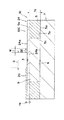
図1に模式的に示すように、光変調システムは、信号源、変調器電極を備える光変調器本体、および終端抵抗を有する。従来は、信号源の特性インピーダンスZiが50Ωであり、変調用電極の特性インピーダンスZcが40-45Ω程度であり、終端抵抗のインピーダンスZlが50Ω程度であった。 As schematically shown in FIG. 1, the optical modulation system includes a signal source, an optical modulator body including modulator electrodes, and a termination resistor. Conventionally, the characteristic impedance Zi of the signal source is 50Ω, the characteristic impedance Zc of the modulation electrode is about 40-45Ω, and the impedance Zl of the terminating resistor is about 50Ω.
しかし、本発明者は、高周波信号を処理する光変調器について変調効率をシミュレーションしたところ、例えば、30GHzにおける変調効率をシミュレーションしてみた。この際、Zc=Zi=Zlとした場合の変調効率を基準とする。得られた結果を表1に示す。ここから、Zc/Zi=1.4かつZl/Zi=1.4とした場合の変調効率は3dB高くなることがわかった。これは、Zc=Zi=Zlとした場合に比べて0.7倍の駆動電圧で駆動可能なことを意味する。 However, the inventor simulated the modulation efficiency of an optical modulator that processes a high-frequency signal, and simulated the modulation efficiency at, for example, 30 GHz. At this time, the modulation efficiency when Zc = Zi = Zl is set as a reference. Table 1 shows the obtained results. From this, it was found that the modulation efficiency when Zc / Zi = 1.4 and Zl / Zi = 1.4 was increased by 3 dB. This means that driving can be performed with a driving voltage 0.7 times as large as that when Zc = Zi = Zl.
一方、特許文献2におけるインピーダンス配分を適用すると、信号源のインピーダンスZiと電極の特性インピーダンスZcは同じ値で、Zc>Zlとすることとなる。これは例えば、表1のシミュレーションにおいて、Zc/Zi=1、Zl/Zi=0.6とすることに相当し、この時変調効率は1.9dB低くなる。これは、Zc=Zi=Zlとした場合と比べて変調効率は逆に低くなり、駆動電圧が増加することを意味する。 On the other hand, when the impedance distribution in Patent Literature 2 is applied, the impedance Zi of the signal source and the characteristic impedance Zc of the electrode have the same value, and Zc> Zl. This corresponds to, for example, setting Zc / Zi = 1 and Zl / Zi = 0.6 in the simulation of Table 1, and at this time, the modulation efficiency is reduced by 1.9 dB. This means that the modulation efficiency is conversely lower than when Zc = Zi = Zl, and the drive voltage increases.
好適な実施形態においては、光変調器がZl<Zcの関係を満足する。図2の例を参照しつつ、更に説明する。 In a preferred embodiment, the optical modulator satisfies the relationship Zl <Zc. This will be further described with reference to the example of FIG.
図2は、変調用電極の特性インピーダンスZcを40Ωに設定し、終端抵抗のインピーダンスZlを30、40、50Ωに変更したときの光応答特性の周波数変化である。従来の光変調器においては、終端抵抗のインピーダンスZlが変調用電極の特性インピーダンスZcよりも高く(Zc<Zl)、図2の破線に示すような特性になっていた。つまり、光応答が、低周波(例えば1GHz周辺)からいったん大きく落ち込み、次いで周波数が高くなるのにつれて単調減少していた。また、光変調器を駆動する信号源も、周波数が高くなるのにつれて利得が単調減少する傾向がある。信号源と光変調器とを合わせたときの変調特性は、光変調器の光応答の周波数特性と、信号源の利得の周波数特性との合成となる。従って、周波数が増加するのにつれて変調特性は急激に落ち込み、1GHz以下の低周波での変調特性と高周波での変調特性との差が大きい。この結果、変調信号の歪みが大きくなるという問題があった。 FIG. 2 shows a frequency change of the optical response characteristic when the characteristic impedance Zc of the modulation electrode is set to 40Ω and the impedance Zl of the terminating resistor is changed to 30, 40, and 50Ω. In the conventional optical modulator, the impedance Zl of the terminating resistor is higher than the characteristic impedance Zc of the modulation electrode (Zc <Zl), and the characteristic is as shown by the broken line in FIG. That is, the optical response once dropped sharply from a low frequency (for example, around 1 GHz), and then monotonically decreased as the frequency increased. Further, the signal source for driving the optical modulator also has a tendency that the gain decreases monotonically as the frequency increases. The modulation characteristic when the signal source and the optical modulator are combined is a combination of the frequency characteristic of the optical response of the optical modulator and the frequency characteristic of the gain of the signal source. Therefore, the modulation characteristics drop sharply as the frequency increases, and the difference between the modulation characteristics at a low frequency of 1 GHz or less and the modulation characteristics at a high frequency is large. As a result, there is a problem that the distortion of the modulation signal increases.
これに対して、終端抵抗のインピーダンスZlよりも変調用電極の特性インピーダンスZcを大きくする(Zl<Zc)ことによって、周波数変化に対する変調信号の歪みを低減できる。例えば図2において一点鎖線の例では、Zl=30Ω、Zc=40Ωであり、終端抵抗のインピーダンスZlを低くしている。この場合には、まず低周波領域において光応答がいったん増大し、次いで周波数増加につれて単調減少する。これに対して、信号源での利得は、周波数増加につれて単調減少する。従って、破線で示す場合に比べて、信号源での利得の減少を相殺する効果があり、全体として変調信号の歪みを低減できる。この結果、信号源および光変調器を合わせた光変調装置全体として、従来に比べてフラットな変調特性を実現でき、変調信号を歪みを抑制することが可能となる。 On the other hand, by making the characteristic impedance Zc of the modulation electrode larger than the impedance Zl of the terminating resistor (Zl <Zc), it is possible to reduce the distortion of the modulation signal due to a frequency change. For example, in the example shown by the dashed line in FIG. 2, Zl = 30Ω and Zc = 40Ω, and the impedance Zl of the terminating resistor is reduced. In this case, the optical response first increases in the low frequency region, and then monotonically decreases as the frequency increases. In contrast, the gain at the signal source monotonically decreases with increasing frequency. Therefore, compared with the case shown by the broken line, there is an effect of offsetting the decrease in gain at the signal source, and the distortion of the modulation signal can be reduced as a whole. As a result, as a whole optical modulation device including a signal source and an optical modulator, a flat modulation characteristic can be realized as compared with the related art, and distortion of a modulation signal can be suppressed.
なお、図2の例では、Zl=30〜50Ω、Zc=40Ωの例について光応答特性を示したが、他の数値条件においてもほぼ同様の結果が得られる。
以上の検討は、信号源インピーダンスZiの値に関わらず有効である。一方、特許文献2においては、一般的なZi=50Ωについてのみ示されている。しかし、前述したとおり、Zi=50ΩとしたままZlのインピーダンス値を下げれば、分圧の法則に従い信号源における入力抵抗で相対的に大きな電圧降下が起きてしまう。このために、変調電極に印加される電圧が相対的に減少し、結果として変調効率が低下し駆動電圧が増加するという欠点があった。このため、ZiはZlあるいはもしくはかつZcより小さくすることが望ましい。
In addition, in the example of FIG. 2, the optical response characteristics are shown for the example of Zl = 30 to 50Ω and Zc = 40Ω, but almost the same result can be obtained under other numerical conditions.
The above examination is valid regardless of the value of the signal source impedance Zi. On the other hand, Patent Document 2 shows only general Zi = 50Ω. However, as described above, if the impedance value of Zl is reduced with Zi = 50Ω, a relatively large voltage drop occurs at the input resistance of the signal source according to the law of voltage division. For this reason, there is a disadvantage that the voltage applied to the modulation electrode relatively decreases, and as a result, the modulation efficiency decreases and the driving voltage increases. For this reason, it is desirable that Zi be smaller than Zl and / or Zc.
本発明の観点からは、信号源の特性インピーダンスZiと終端抵抗のインピーダンスZlとの差は、1Ω以上であることが好ましく、3Ω以上であることが更に好ましい。 From the viewpoint of the present invention, the difference between the characteristic impedance Zi of the signal source and the impedance Zl of the terminating resistor is preferably 1Ω or more, and more preferably 3Ω or more.
ただし、信号源の特性インピーダンスZiが小さくなると、変調器電極と信号源でのインピーダンス不整合から反射が生じ、信号源の安定性が低下する。この観点からは、ZiとZlとの差は、30Ω以下であることが好ましい。 However, when the characteristic impedance Zi of the signal source decreases, reflection occurs due to impedance mismatch between the modulator electrode and the signal source, and the stability of the signal source decreases. From this viewpoint, the difference between Zi and Zl is preferably 30Ω or less.
本発明の観点からは、信号源の特性インピーダンスZiと変調用電極の特性インピーダンスZcとの差は、1Ω以上であることが好ましく、3Ω以上であることが更に好ましい。 From the viewpoint of the present invention, the difference between the characteristic impedance Zi of the signal source and the characteristic impedance Zc of the modulation electrode is preferably 1Ω or more, and more preferably 3Ω or more.
ただし、上記の理由から、ZiとZcとの差は、30Ω以下であることが好ましい。 However, for the above reason, the difference between Zi and Zc is preferably 30Ω or less.
変調特性のフラット化という観点からは、終端抵抗のインピーダンスZlと変調用電極の特性インピーダンスZcとの差は、5Ω以上であることが好ましく、10Ω以上であることが更に好ましい。 From the viewpoint of flattening the modulation characteristics, the difference between the impedance Zl of the terminating resistor and the characteristic impedance Zc of the modulation electrode is preferably 5Ω or more, and more preferably 10Ω or more.
また、従来の進行波形光変調器においては、信号源の特性インピーダンスZiは通常50Ωに規格化されていた。しかし、本発明においては、前述のように、信号源の特性インピーダンスZiを、変調用電極や終端抵抗のインピーダンスよりも小さくする。この際、信号源の特性インピーダンスZiが50Ωであると、変調用電極の特性インピーダンスZcを50Ωよりも十分に大きくすることが、材料特性および変調器の設計の観点から難しい。このため、ZcとZiとの差を十分に大きくするという観点からは、信号源の特性インピーダンスZiを50Ω以下とすることが好ましく、45Ω以下とすることが更に好ましい。 In the conventional traveling-wave optical modulator, the characteristic impedance Zi of the signal source is usually standardized to 50Ω. However, in the present invention, as described above, the characteristic impedance Zi of the signal source is made smaller than the impedance of the modulation electrode or the terminating resistor. At this time, if the characteristic impedance Zi of the signal source is 50Ω, it is difficult to make the characteristic impedance Zc of the modulation electrode sufficiently larger than 50Ω from the viewpoint of the material characteristics and the design of the modulator. Therefore, from the viewpoint of sufficiently increasing the difference between Zc and Zi, the characteristic impedance Zi of the signal source is preferably set to 50Ω or less, more preferably 45Ω or less.
上記した第一の態様に係る発明の各実施形態は、後述する第二の態様に係る発明において採用できるものである。 Each embodiment of the invention according to the first aspect described above can be employed in the invention according to the second aspect described below.
第二の態様に係る発明は、電気光学材料からなり、相対向する一方の主面と他方の主面とを備えている基板本体、この基板本体に形成されている光導波路、および基板本体に設けられ、光導波路を伝搬する光を変調するための電圧を印加する変調用電極を備えている光変調器であって、
変調用電極がコプレーナ型電極配置に従って設けられており、変調用電極における電極間ギャップが38μm以下であり、光導波路の設置領域における基板本体の厚さが20μm以下であることを特徴とする。
The invention according to a second aspect is directed to a substrate body made of an electro-optical material and having one main surface and the other main surface facing each other, an optical waveguide formed on the substrate main body, and a substrate main body. Provided is an optical modulator including a modulation electrode for applying a voltage for modulating light propagating in the optical waveguide,
The modulation electrode is provided according to the coplanar electrode arrangement, the interelectrode gap in the modulation electrode is 38 μm or less, and the thickness of the substrate body in the installation region of the optical waveguide is 20 μm or less.
このように電極間ギャップを小さくし、かつ光導波路の設置領域における基板本体の厚さを20μm以下とすることによって、速度整合を実現できるのと共に、光変調器の駆動電圧を著しく低減することに成功し、本発明に到達した。 By reducing the gap between the electrodes and setting the thickness of the substrate body to 20 μm or less in the installation region of the optical waveguide, speed matching can be realized and the driving voltage of the optical modulator can be significantly reduced. Succeeded and reached the present invention.
電極間ギャップを小さくすると、光導波路に印加される電界が強くなるので、駆動電圧を低減できることは知られている。また、基板本体の厚さを小さくすることによって、速度整合を実現可能なことも知られている(特開平10−133159号公報参照)。しかし、本発明者は、電極間ギャップを38μm以下とした場合に、同時に基板本体の厚さを20μm以下にすることによって、駆動電圧が相乗的に顕著に低減されることを見出した。 It is known that when the gap between the electrodes is reduced, the electric field applied to the optical waveguide is increased, so that the drive voltage can be reduced. It is also known that speed matching can be realized by reducing the thickness of the substrate body (see Japanese Patent Application Laid-Open No. 10-133159). However, the present inventor has found that when the inter-electrode gap is 38 μm or less, the drive voltage is remarkably reduced synergistically by simultaneously reducing the thickness of the substrate body to 20 μm or less.
好適な実施形態では、変調用電極の電極間ギャップが38μm以下であり、これによって駆動電圧を一層低減できる。 In a preferred embodiment, the inter-electrode gap of the modulation electrode is 38 μm or less, so that the driving voltage can be further reduced.
好適な実施形態においては、基板本体に接合されている保持基体を設ける。これによって、基板本体に取り扱い可能な機械的強度を付与できる。しかし、保持基体を備えた光変調器では、低誘電率材料と変調器本体に用いる電気光学材料の熱膨張差によって内部応力が発生し、この応力に起因するクラックが電気光学結晶で発生し問題となっていた。また、この内部応力は変調動作の安定性低下も引き起こしていた。 In a preferred embodiment, a holding substrate joined to the substrate body is provided. Thereby, mechanical strength that can be handled can be imparted to the substrate body. However, in an optical modulator having a holding substrate, internal stress is generated due to a difference in thermal expansion between a low dielectric constant material and an electro-optical material used for the modulator body, and cracks caused by the stress are generated in the electro-optical crystal. It was. In addition, the internal stress also caused a decrease in the stability of the modulation operation.
この内部応力について有限要素法を用いて詳細な検討を行った結果、低誘電率材料の厚さを10μmとすれば、厚さ200ミクロンの厚さの時に比べ、低誘電率層と変調器本体基板界面で生じる応力は1/5以下となり、大幅に応力を小さくすることができる事がわかった。この結果、低誘電率材料を200ミクロン以下、さらに好ましくは150μm以下、もっとも好ましくは110μm以下に薄くすることで、内部応力を大幅に小さくできることがわかった。 As a result of a detailed study of this internal stress using the finite element method, assuming that the thickness of the low dielectric constant material is 10 μm, the low dielectric constant layer and the modulator body are compared with the case of a thickness of 200 μm. The stress generated at the substrate interface was reduced to 1/5 or less, indicating that the stress could be significantly reduced. As a result, it was found that the internal stress can be significantly reduced by reducing the thickness of the low dielectric constant material to 200 μm or less, more preferably 150 μm or less, and most preferably 110 μm or less.
しかし、低誘電率層を薄くすると、保持基体までしみ出す電界の割合が増加し、マイクロ波実効屈折率が上昇するために、速度整合を達成できなくなり、変調帯域が低下する。 However, when the low dielectric constant layer is made thin, the ratio of the electric field that exudes to the holding substrate increases, and the effective refractive index of the microwave increases, so that speed matching cannot be achieved and the modulation band decreases.
しかしながら、電極間ギャップを38μm以下に狭くすれば、電極からの電界の広がりは小さくなり、より薄い低誘電率層で速度整合が可能となる。この結果、内部応力を低減することが可能となり、歩留まりの高い状態で光変調器を製造することが可能となる。
低誘電率層の厚みを200ミクロン以上とした光変調器では、−40℃〜+80℃、1000サイクルの熱衝撃試験に対して変調器本体基板にクラックが発生しやすいという問題があった。しかし、接着層厚を200ミクロン以下とすることで、内部応力低減を図った結果、クラックの発生が減少することを確認した。例えば、接着層の厚さを200μmとした時、50個作製中クラック発生はなくなり、本発明適用による信頼性の大幅な改善を確認した。
However, if the gap between the electrodes is reduced to 38 μm or less, the spread of the electric field from the electrodes is reduced, and the speed matching can be performed with a thinner low dielectric constant layer. As a result, the internal stress can be reduced, and the optical modulator can be manufactured with a high yield.
An optical modulator having a low dielectric constant layer having a thickness of 200 μm or more has a problem that cracks are easily generated on the modulator main body in a thermal shock test at −40 ° C. to + 80 ° C. for 1000 cycles. However, it was confirmed that the internal stress was reduced by setting the thickness of the adhesive layer to 200 microns or less, and as a result, the occurrence of cracks was reduced. For example, when the thickness of the adhesive layer was 200 μm, no crack was generated during the production of 50 pieces, and it was confirmed that the application of the present invention significantly improved the reliability.
好適な実施形態においては、インピーダンス整合の観点からは電極間ギャップを狭くするほど基板本体の厚さを薄くする必要がある。好ましい実施形態において光導波路の設置領域における基板本体の厚さが15μm以下であり、一層好ましくは10μm以下である。これによって、駆動電圧が一層低減される。 In a preferred embodiment, from the viewpoint of impedance matching, it is necessary to reduce the thickness of the substrate body as the gap between the electrodes is reduced. In a preferred embodiment, the thickness of the substrate main body in the installation region of the optical waveguide is 15 μm or less, and more preferably 10 μm or less. Thereby, the driving voltage is further reduced.
なお、特開平10−133159号公報の記載では、基板の厚さを10μm以下とすることは、光導波路の光損失が大きくなる傾向があるので難しいとされている。しかし、本発明者が更に検討を進めたところ、機械加工を適切に行えば、厚さ10μm以下であっても光損失の小さい光導波路を形成可能なことがわかってきた。そして、このように薄い基板本体に光導波路を設けることで、駆動電圧の顕著な低減を可能とした。 According to Japanese Patent Application Laid-Open No. Hei 10-133159, it is difficult to reduce the thickness of the substrate to 10 μm or less because the optical loss of the optical waveguide tends to increase. However, as a result of further study by the present inventor, it has been found that an optical waveguide having a small optical loss can be formed even if the thickness is 10 μm or less, by appropriately performing machining. By providing the optical waveguide on the thin substrate body, the driving voltage can be remarkably reduced.
図3、図4には、基板本体(ニオブ酸リチウム基板)の厚さ、光変調器の電極間ギャップ、および半波長電圧と電極長との積(Vcm)の関係を示す。電極間ギャップを小さくすると、半波長電圧と電極長との積が低下する。これだけでなく、基板本体の厚さが小さくなると、半波長電圧と電極長との積が低下することが分かる。 3 and 4 show the relationship between the thickness of the substrate body (lithium niobate substrate), the gap between the electrodes of the optical modulator, and the product (Vcm) of the half-wave voltage and the electrode length. When the gap between the electrodes is reduced, the product of the half-wave voltage and the electrode length decreases. Not only this, but when the thickness of the substrate body is reduced, the product of the half-wave voltage and the electrode length is reduced.
また、本発明は、電気光学材料からなり、相対向する一方の主面と他方の主面とを備えている基板本体、この基板本体に形成されている光導波路、および基板本体に設けられ、光導波路を伝搬する光を変調するための電圧を印加する変調用電極を備えている光変調器であって、
変調用電極が非対称コプレーナストリップライン型電極配置に従って設けられており、変調用電極における電極間ギャップが19μm以下であり、光導波路の設置領域における基板本体の厚さが20μm以下であることを特徴とする。
Further, the present invention is provided in the substrate body, which is made of an electro-optical material and has one main surface and the other main surface facing each other, an optical waveguide formed in the substrate main body, and provided in the substrate main body, An optical modulator comprising a modulation electrode for applying a voltage for modulating light propagating through an optical waveguide,
The modulation electrode is provided according to an asymmetric coplanar stripline type electrode arrangement, the gap between the electrodes in the modulation electrode is 19 μm or less, and the thickness of the substrate body in the installation region of the optical waveguide is 20 μm or less. I do.
この発明に係る光変調器は、いわゆる非対称コプレーナストリップライン型の電極配置に適用される。この発明も上記と同様の効果を示す。ただし、電極配置が非対称コプレーナストリップラインであることから、電極間ギャップの値が半分(19μm以下)となっている。 The optical modulator according to the present invention is applied to a so-called asymmetric coplanar stripline type electrode arrangement. The present invention also has the same effect as described above. However, since the electrode arrangement is an asymmetric coplanar stripline, the value of the gap between the electrodes is half (19 μm or less).
フィードスルー部でコネクタピンと接続をするために中心電極幅を広くする、かつ、もしくは、保持基板表面に導電層をもうけて電磁波をシールドして高周波特性の改善を図ると光変調器のフィードスルー部の特性インピーダンスが低下する傾向があり、このために信号源の特性インピーダンスZiと合わなくなる可能性がある。このため、第二の態様に係る発明においては、基板本体の直下に、基板本体を構成する電気光学材料の誘電率よりも低い誘電率を有する低誘電率部分を設けることができる。これによって、光変調器のフィードスルー部の特性インピーダンスを向上させることができる。 If the width of the center electrode is widened to connect to the connector pin in the feedthrough part, or if a conductive layer is provided on the holding substrate surface to shield electromagnetic waves and improve high frequency characteristics, the feedthrough part of the optical modulator Characteristic impedance tends to decrease, which may result in a mismatch with the characteristic impedance Zi of the signal source. For this reason, in the invention according to the second aspect, a low dielectric constant portion having a dielectric constant lower than the dielectric constant of the electro-optical material forming the substrate main body can be provided directly below the substrate main body. Thereby, the characteristic impedance of the feed-through portion of the optical modulator can be improved.
また、第一の発明の実施形態を第二の発明に適用した場合には、さらに電極間ギャップを狭くすることができるために、さらに低駆動電圧を図ることができる。以下に詳しく説明する。 Further, when the embodiment of the first invention is applied to the second invention, the gap between the electrodes can be further narrowed, so that a lower driving voltage can be achieved. This will be described in detail below.
電極間ギャップを狭くすると同時に電極のマイクロ波特性インピーダンスも低下する。このため、従来の50Ω系でインピーダンスマッチングを前提とした変調器の適用法ではインピーダンス不整合により低周波で変調器光応答特性が大きく落ち込み、変調帯域が大幅に減少するという欠点があった。 At the same time as the gap between the electrodes is reduced, the microwave characteristic impedance of the electrodes is also reduced. For this reason, the conventional method of applying a modulator on the premise of impedance matching in a 50Ω system has a drawback that the optical response characteristics of the modulator are greatly reduced at a low frequency due to impedance mismatch, and the modulation band is greatly reduced.
前述の通り電極間ギャップを狭くするのに伴い変調器本体の基板の厚さを薄くすることで、特性インピーダンスを50Ωへ近づけることは可能である。しかし、例えば基板厚さを3μm以下とすることは、基板強度の面、及び光導波路のモードサイズが小さくなるため光ファイバーとの結合損失が増大するために難しい。すなわち、変調器電極間ギャップの実施可能な最小値は、実質的に加工が容易で利用可能な変調器本体基板厚さの最小値に制約されていた。 As described above, it is possible to make the characteristic impedance close to 50Ω by reducing the thickness of the substrate of the modulator body as the gap between the electrodes is reduced. However, it is difficult to reduce the thickness of the substrate to 3 μm or less, for example, because the surface of the substrate strength and the mode size of the optical waveguide are reduced, and the coupling loss with the optical fiber increases. In other words, the practicable minimum value of the modulator electrode gap is substantially restricted to the minimum value of the modulator body substrate thickness which can be easily processed and used.
しかし、第二の発明を適用し、インピーダンス配分を最適化することで、低特性インピーダンスの光変調器においても効率のよい変調動作を行うことができるために、電気光学基板厚さの最小値に制約されることなく、さらに電極間ギャップを狭くすることが可能となる。このため、第一の発明のみを適用した場合と比べ、さらに低駆動電圧化を実現することができる。 However, by applying the second invention and optimizing the impedance distribution, an efficient modulation operation can be performed even in an optical modulator having a low characteristic impedance. Without being restricted, it is possible to further narrow the gap between the electrodes. Therefore, a lower driving voltage can be realized as compared with the case where only the first invention is applied.
第二の態様に係る発明およびその実施形態は、上述した第一の態様に係る発明の実施の際に適用可能なものである。 The invention according to the second aspect and the embodiments thereof are applicable when the invention according to the first aspect is implemented.
以下、第一の態様、第二の態様に係る発明に適用可能な実施形態を更に詳細に説明する。 Hereinafter, embodiments applicable to the inventions according to the first and second aspects will be described in more detail.
図5は、第一の態様、第二の態様において利用可能な光変調器1Aを概略的に示す断面図である。 FIG. 5 is a cross-sectional view schematically showing an optical modulator 1A usable in the first embodiment and the second embodiment.
光変調器1Aは、光導波路基板10Aと保持基体7とを備えている。基板本体4、基体7は共に平板形状をしている。基板本体4の一方の主面4aの上には所定の電極2A、2B、2Cが形成されている。本例では、いわゆるコプレーナ型(Coplanar
waveguide:CPW電極) の電極配置を採用している。本例では、隣接する電極の間に一対の光導波路3が形成されており,各光導波路3に対して略水平方向に信号電圧を印加するようになっている。各光導波路3は、平面的に見るといわゆるマッハツェンダー型の光導波路を構成しているが、この平面的パターンそれ自体は周知であるので図示省略する。本体4の他方の主面4b側には凹部4eが形成されており、凹部4eに対して、2つの第二の肉薄部分4dと1つの第一の肉薄部分4fとが面している。4fは一対の肉薄部分4dによって挟まれている。各肉薄部分4dの外側には基部4gが設けられている。
The optical modulator 1A includes an optical waveguide substrate 10A and a holding
A waveguide (CPW electrode) electrode arrangement is employed. In this example, a pair of
保持基体7の一方の主面7aが、基板本体4の他方の主面4bに対して、接合層5を介して接合されている。5a、5bは接着面であり、5cは空隙部分6への露出面である。
One main surface 7a of the holding
このようなデバイスによれば、デバイス全体の強度は、比較的に肉厚な保持基体7によって保持できるので、デバイス全体に取り扱い可能な強度を付与でき、かつ基板本体4の反りも生じない。これと共に、基板本体4の肉薄部4fの厚さtwは例えば20μm以下と薄くできる。これによって、電極を伝搬するマイクロ波の伝搬速度を大きくすることができ、かつ前述のように駆動電圧を低減できる。
According to such a device, the strength of the entire device can be held by the relatively
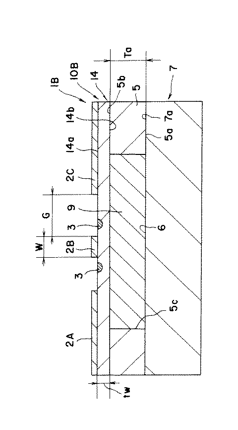
図6に示す進行波形光変調器1Bは、光導波路基板10Bと保持基体7とを備えている。保持基体7は平板状であり、かつ基板本体14も平板状である。本例では、空隙部分6内に、基板本体14を構成する電気光学材料の誘電率よりも低い誘電率を有する低誘電率材料9が充填されている。また、基板本体14の一方の主面14aの上には所定の電極2A、2B、2Cが形成されている。基板本体14の主面14bと保持基体7とが接合層5を介して接合されている。
The traveling waveform optical modulator 1B shown in FIG. 6 includes an optical waveguide substrate 10B and a holding
図7の光変調器1Cは、光導波路基板10B、保持基体7および両者を接合する接合層15からなる。光導波路基板1Bの基板本体14は、図6の例と同様に平板状である。基板本体14上には、コプレーナ型の電極2A、2B、2Cが形成されている。接合層15の主面15bが基板本体14の主面14bに接触しており、主面15aが保持基体7の主面7aに接触している。
The optical modulator 1C of FIG. 7 includes an optical waveguide substrate 10B, a holding
図8の光変調器1Dは、光導波路基板10Cと保持基体7とを備えている。保持基体7は平板状であり、かつ基板本体24も平板状である。基板本体24の他方の主面24bは接合層5によって保持基体7に接合されている。本例では、空隙部分6内に、基板本体24を構成する電気光学材料の誘電率よりも低い誘電率を有する低誘電率材料9が充填されている。また、基板本体24の一方の主面24aの上には所定の電極2D、2Eが形成されており、いわゆる非対称コプレーナストリップライン(Asymmetric
coplanar strip line:A−CPS電極) 型の電極配置を採用している。隣接する電極の間に光導波路3が形成されており,光導波路3に対して略水平方向に信号電圧を印加するようになっている。基板本体14の厚さtwは、第二の態様に係る発明においては20μm以下とする。
The optical modulator 1D of FIG. 8 includes an
A coplanar strip line (A-CPS electrode) type electrode arrangement is employed. An
本発明は、いわゆる独立変調型の進行波形光変調器に対しても適用可能である。 The present invention is also applicable to a so-called independent modulation type traveling waveform optical modulator.
好適な実施形態においては、図6、図7、図8に例示するように、少なくとも基板本体の他方の主面に対して、電気光学材料の誘電率よりも低い誘電率を有する低誘電率材料9が接触するように構成する。これによって、薄い基板本体をその他方の主面側から直接に補強することができる。低誘電率材料としては、ガラス、エポキシ系あるいはアクリル系などの接着剤、あるいは半導体製造用層間絶縁体、ポリイミドを例示できる。 In a preferred embodiment, as illustrated in FIGS. 6, 7, and 8, a low dielectric constant material having a dielectric constant lower than the dielectric constant of the electro-optic material, at least with respect to the other main surface of the substrate body. 9 are configured to be in contact with each other. Thereby, the thin substrate main body can be reinforced directly from the other main surface side. Examples of the low dielectric constant material include glass, an epoxy-based or acrylic-based adhesive, an interlayer insulator for semiconductor production, and polyimide.
基板本体は、強誘電性の電気光学材料、好ましくは単結晶からなる。こうした結晶は、光の変調が可能であれば特に限定されないが、ニオブ酸リチウム、タンタル酸リチウム、ニオブ酸リチウム−タンタル酸リチウム固溶体、ニオブ酸カリウムリチウム、KTP、GaAs及び水晶などを例示することができる。ニオブ酸リチウム単結晶、タンタル酸リチウム単結晶、ニオブ酸リチウム−タンタル酸リチウム固溶体単結晶が、特に好ましい。 The substrate body is made of a ferroelectric electro-optic material, preferably a single crystal. Such a crystal is not particularly limited as long as light can be modulated. Examples thereof include lithium niobate, lithium tantalate, lithium niobate-lithium tantalate solid solution, potassium lithium niobate, KTP, GaAs, and quartz. it can. Particularly preferred are lithium niobate single crystal, lithium tantalate single crystal, and lithium niobate-lithium tantalate solid solution single crystal.
電極は、低抵抗でインピーダンス特性に優れる材料であれば特に限定されるものではなく、金、銀、銅などの材料から構成することができる。 The electrode is not particularly limited as long as it is a material having low resistance and excellent impedance characteristics, and may be made of a material such as gold, silver, or copper.
保持基体によるマイクロ波の伝搬速度への影響を最小限とするという観点からは、保持基体の材質は、電気光学単結晶の誘電率よりも低い誘電率を有する材質であることが好ましい。こうした材質としては、石英ガラス等のガラスがある。 From the viewpoint of minimizing the effect of the holding base on the propagation speed of the microwave, the holding base is preferably made of a material having a dielectric constant lower than that of the electro-optic single crystal. Such materials include glass such as quartz glass.
基板本体の表面(一方の主面)と電極との間にはバッファ層を設けることができる。バッファ層は、酸化シリコン、弗化マグネシウム、窒化珪素、及びアルミナなどの公知の材料を使用することができる。 A buffer layer can be provided between the surface (one main surface) of the substrate body and the electrode. Known materials such as silicon oxide, magnesium fluoride, silicon nitride, and alumina can be used for the buffer layer.
光導波路は、基板本体に形成されており、好ましくは基板本体の一方の主面側に形成されている。光導波路は、基板本体の一方の主面に直接形成されたリッジ型の光導波路であってよく、基板本体の一方の主面の上に他の層を介して形成されたリッジ型の光導波路であってよく、また基板本体の内部に内拡散法やイオン交換法によって形成された光導波路、例えばチタン拡散光導波路、プロトン交換光導波路であってよい。電極は、基板本体の一方の主面側に設けられているが、基板本体の一方の主面に直接形成されていてよく、バッファ層の上に形成されていてよい。 The optical waveguide is formed on the substrate main body, and is preferably formed on one main surface side of the substrate main body. The optical waveguide may be a ridge-type optical waveguide formed directly on one main surface of the substrate main body, and a ridge-type optical waveguide formed on one main surface of the substrate main body via another layer. Or an optical waveguide formed inside the substrate body by an internal diffusion method or an ion exchange method, for example, a titanium diffusion optical waveguide or a proton exchange optical waveguide. Although the electrode is provided on one main surface side of the substrate main body, it may be formed directly on one main surface of the substrate main body or may be formed on the buffer layer.
基板本体においては、特に好ましくは結晶の分極軸が基板の一方の主面(表面)と略水平である。この場合には、ニオブ酸リチウム単結晶、タンタル酸リチウム単結晶、ニオブ酸リチウム−タンタル酸リチウム固溶体単結晶からなるX板あるいはY板が好ましい。図5〜図8には、本発明をX板あるいはY板に適用した例について示した。 In the substrate body, the polarization axis of the crystal is particularly preferably substantially horizontal to one main surface (front surface) of the substrate. In this case, an X plate or a Y plate made of lithium niobate single crystal, lithium tantalate single crystal, or lithium niobate-lithium tantalate solid solution single crystal is preferable. 5 to 8 show examples in which the present invention is applied to an X plate or a Y plate.
また、他の好適な実施形態においては、結晶の分極軸が基板の一方の主面(表面)と略垂直である。この場合には、ニオブ酸リチウム単結晶、タンタル酸リチウム単結晶、ニオブ酸リチウム−タンタル酸リチウム固溶体単結晶からなるZ板が好ましい。Z板を使用した場合には、光導波路は電極の直下に設ける必要があり、光の伝搬損失を低減するために、基板の表面と電極との間にはバッファ層を設けることが好ましい。 In another preferred embodiment, the polarization axis of the crystal is substantially perpendicular to one main surface (surface) of the substrate. In this case, a Z plate made of a lithium niobate single crystal, a lithium tantalate single crystal, or a lithium niobate-lithium tantalate solid solution single crystal is preferable. When a Z plate is used, the optical waveguide needs to be provided immediately below the electrode, and a buffer layer is preferably provided between the surface of the substrate and the electrode in order to reduce light propagation loss.
また、好適な実施形態においては、図5に示すように、基板本体が、凹部に面する相対的に厚さの大きい第一の肉薄部分と、凹部に面する相対的に厚さの小さい第二の肉薄部分とを備えており、光導波路が第一の肉薄部分内に設けられている。 In a preferred embodiment, as shown in FIG. 5, the substrate main body has a first thin portion having a relatively large thickness facing the concave portion and a first thin portion having a relatively large thickness facing the concave portion. An optical waveguide is provided in the first thinned portion.
光導波路基板と保持基体との接合方法は特に限定されない。好適な実施形態においては、両者を接着する。この場合には、接着剤の屈折率は、基板本体を構成する電気光学材料の屈折率よりも低いことが好ましい。これに加えて、接着剤の誘電率は、基板本体を構成する電気光学材料の誘電率よりも低いことが望ましい。 The joining method of the optical waveguide substrate and the holding base is not particularly limited. In a preferred embodiment, the two are adhered. In this case, it is preferable that the refractive index of the adhesive is lower than the refractive index of the electro-optical material forming the substrate body. In addition, the dielectric constant of the adhesive is desirably lower than the dielectric constant of the electro-optic material forming the substrate body.
接着剤の具体例は、前記の条件を満足する限り特に限定されないが、エポキシ系接着剤、熱硬化型接着剤、紫外線硬化性接着剤、ニオブ酸リチウムなどの電気光学効果を有する材料と比較的近い熱膨張係数を有するアロンセラミックスC(商品名、東亜合成社製)(熱膨張係数13×10−6/K)を例示できる。 Specific examples of the adhesive are not particularly limited as long as the above-mentioned conditions are satisfied, but are relatively different from materials having an electro-optical effect such as an epoxy-based adhesive, a thermosetting adhesive, an ultraviolet-curable adhesive, and lithium niobate. Aron ceramics C (trade name, manufactured by Toa Gosei Co., Ltd.) having a similar thermal expansion coefficient (thermal expansion coefficient: 13 × 10 −6 / K) can be exemplified.
また、図5〜図8の光変調器を製造するためには、基板本体の裏面と保持基体との間に接合材のシートを介在させ、接合する。好ましくは、熱硬化性、光硬化性あるいは光増粘性の樹脂接着剤からなるシートを、基板本体の裏面と保持基体との間に介在させ、シートを硬化させる。このようなシートとしては、以下を例示できる。
300μm以下のフィルム樹脂が適当であり、具体的に日立化成製のT−2000、日清紡製カルボジライトフィルム、ナガセケムテック製A−1400,A−1500、A−1600がある。
Further, in order to manufacture the optical modulators shown in FIGS. 5 to 8, a sheet of a bonding material is interposed between the back surface of the substrate main body and the holding base and bonded. Preferably, a sheet made of a thermosetting, photo-curing or photo-viscosifying resin adhesive is interposed between the back surface of the substrate main body and the holding base to cure the sheet. Examples of such a sheet include the following.
A film resin having a thickness of 300 μm or less is suitable. Specific examples include T-2000 manufactured by Hitachi Chemical, Carbodilite Film manufactured by Nisshinbo, and A-1400, A-1500, and A-1600 manufactured by Nagase Chemtech.
特に、図5〜図8に示すように、平板形状の保持基体26を使用し、基板本体と保持基体とを樹脂接着剤シートによって接着する場合には、保持基体側に凹部を形成する処理が不要であるので、極めて生産性が高い。 In particular, as shown in FIGS. 5 to 8, when a flat holding base 26 is used and the substrate body and the holding base are bonded with a resin adhesive sheet, a process of forming a concave portion on the holding base side is required. Since it is unnecessary, the productivity is extremely high.
(製造例)
図6に示す光変調器1Bを製造した。例えばXカットした3インチウエハー(LiNbO3単結晶)からなる基板を使用し、チタン拡散プロセスとフォトリソグラフィー法とによって、ウエハーの表面にマッハツェンダー型の光導波路3を形成する。光導波路3のサイズは、例えば1/e2で10μmとできる。次いで、メッキプロセスにより、CPW電極を形成した。
(Production example)
The optical modulator 1B shown in FIG. 6 was manufactured. For example, a substrate made of an X-cut 3-inch wafer (LiNbO 3 single crystal) is used, and a Mach-Zehnder
このウエハー形状の基板本体の素材の一方の主面(表面)にレジスト膜をコーティングし、ニオブ酸リチウムからなるベース基板と熱可塑性樹脂によって貼り合わせた後、変調器基板の裏面4b側に横型研磨、高速ラップ、及びポリッシング(CMP)を施して研磨処理を行なった。基板厚さは形状測定器を用いて計測し所望の基板厚に制御した。
One main surface (front surface) of the material of the wafer-shaped substrate body is coated with a resist film, bonded to a base substrate made of lithium niobate with a thermoplastic resin, and then horizontally polished on the
次いで、基板本体4と保持基体7との間に、厚さ50μmのエポキシ系熱硬化型樹脂からなるシートを挟み、80℃で加熱することによってシートを熱硬化させ、接合層5を生成させ、基板本体4と保持基体7とを接着した。この際、接合層5の内側には、シートと同じエポキシ樹脂(もしくは空気)を充填した。次に、ウエハーを定盤から取り外し、有機溶剤を用いた洗浄によってステッキワックスを除去した。ウエハーをダイシングソー加工機で切断し、各光変調器チップ1Bに分割した。各チップの光導波路の端面を光学研磨した。
Next, a 50 μm-thick sheet made of an epoxy-based thermosetting resin is sandwiched between the substrate body 4 and the holding
(シミュレーション1)
上記の光変調器1Bについて、有限要素法(FEM) を用いた数値計算による実施例を行った。ここで、基板本体4の厚さtwを13μmとし、中心電極幅Wを30 μmとし、電極間ギャップGを40μmとし、低誘電率材料9の厚さTaは十分に厚くした。得られたマイクロ波特性を用いてインピーダンスZi、Zl、Zcの大小関係を変えたときの変調効率の比較を行った。計算はIEE Proceeding Optoelrctronics, Vol. 146, No2, pp.99-104, April 1999掲載のO.MitomiほかEstimation of
frequency response for high-speed LiNbO3 optical modulators に基づいて行った。計算例では、速度整合が達成されている信号源の特性インピーダンスZiは50Ωとした。Ziに対する終端抵抗のインピーダンスZlおよび変調用電極の特性インピーダンスZcの比率を、表1に示すように変更した。30GHzのマイクロ波について、Zi=Zl=Zcの場合の変調波出力を基準として、Zc/Zi、Zl/Ziを、それぞれ表1に示すように変更し、Zi=Zl=Zcの場合の変調効率に対する変調効率の変化を計算した。この結果を表1に示す。
(Simulation 1)
For the above optical modulator 1B, an example was performed by numerical calculation using the finite element method (FEM). Here, the thickness tw of the substrate body 4 was 13 μm, the center electrode width W was 30 μm, the gap G between the electrodes was 40 μm, and the thickness Ta of the low dielectric
Frequency response for high-speed LiNbO3 optical modulators. In the calculation example, the characteristic impedance Zi of the signal source for which the speed matching is achieved is set to 50Ω. The ratio between the impedance Zl of the terminating resistor and the characteristic impedance Zc of the modulation electrode with respect to Zi was changed as shown in Table 1. For a microwave of 30 GHz, Zc / Zi and Zl / Zi are respectively changed as shown in Table 1 with reference to the modulated wave output when Zi = Zl = Zc, and the modulation efficiency when Zi = Zl = Zc The change in modulation efficiency with respect to was calculated. Table 1 shows the results.
(シミュレーション2)
上記の光変調器1Bについて、有限要素法(FEM) を用いた数値計算による実施例を行った。ここで、基板本体4の厚さtwを13μmとし、中心電極幅Wを30μmとし、電極間ギャップGを40μmとし、低誘電率材料9の厚さTaは十分に厚いとした。信号源の特性インピーダンスZiを50Ωとし、終端抵抗のインピーダンスZlおよび変調用電極の特性インピーダンスZcを、図2に示すように変更した。そして、0〜50GHzの範囲内で光応答特性を計算した。この結果を図2に示す。
(Simulation 2)
For the above optical modulator 1B, an example was performed by numerical calculation using the finite element method (FEM). Here, the thickness tw of the substrate body 4 was 13 μm, the center electrode width W was 30 μm, the gap G between the electrodes was 40 μm, and the thickness Ta of the low dielectric
(シミュレーション3)
上記の光変調器1Bについて、有限要素法(FEM) を用いた数値計算による実施例を行った。ここで、中心電極幅Wを30μmとし、低誘電率材料9の厚さTaを50μmとした。基板本体4の厚さtw、電極間ギャップGを、図3に示すように変更した。そして低周波における半波長電圧と電極長との積を計算し、結果を図3に示す。
(Simulation 3)
For the above optical modulator 1B, an example was performed by numerical calculation using the finite element method (FEM). Here, the center electrode width W was set to 30 μm, and the thickness Ta of the low dielectric
(シミュレーション4)
上記の光変調器1Bについて、有限要素法(FEM) を用いた数値計算による実施例を行った。ここで、中心電極幅Wを10μmとし、低誘電率材料9の厚さTaを50μmとした。基板本体4の厚さtw、電極間ギャップGを、図4に示すように変更した。そして低周波における半波長電圧と電極長との積を計算し、結果を図4に示す。
(Simulation 4)
For the above optical modulator 1B, an example was performed by numerical calculation using the finite element method (FEM). Here, the center electrode width W was set to 10 μm, and the thickness Ta of the low dielectric
以上述べたように、本発明によれば、光変調器の速度整合条件を満足しつつ、かつ高周波帯域において変調効率を改善できる。 As described above, according to the present invention, the modulation efficiency can be improved in a high frequency band while satisfying the speed matching condition of the optical modulator.
1A、1B、1C、1D 光変調器 2A、2B、2C
コプレーナ型配置電極 2D、2E 非対称コプレーナストリップライン型配置電極 3 光導波路 4、14、24 基板本体 4a、14a、24a 基板本体の一方の主面 4b、14b、24b 基板本体の他方の主面 5 低誘電率材料からなる接合層 6 空隙部分 7 保持基体 9 低誘電率材料 15 低誘電率材料からなる接合層 G 電極間ギャップ W 中心電極幅 tw 光導波路形成領域における基板本体の厚さ Zi 信号源の特性インピーダンス Zl 終端抵抗のインピーダンス Zc 変調用電極の特性インピーダンス
1A, 1B, 1C,
Claims (30)
前記信号源の特性インピーダンスZiおよび前記終端抵抗のインピーダンスZlが以下の関係を満足することを特徴とする、光変調器。
Zi<Zl An optical modulator comprising: an optical waveguide; and a modulation electrode for applying a voltage for modulating light propagating through the optical waveguide, wherein a signal source and a terminating resistor are connected to the modulation electrode. hand,
An optical modulator, wherein the characteristic impedance Zi of the signal source and the impedance Zl of the terminating resistor satisfy the following relationship.
Zi <Zl
Zi<Zc The optical modulator according to claim 1, wherein the following relationship is satisfied when the characteristic impedance of the modulation electrode is Zc.
Zi <Zc
Zl<Zc 3. The optical modulator according to claim 1, wherein the following relationship is satisfied when the characteristic impedance of the modulation electrode is Zc.
Zl <Zc
前記信号源の特性インピーダンスZi、および前記変調用電極の特性インピーダンスZcが以下の関係を満足することを特徴とする、光変調器。
Zi<Zc An optical modulator comprising: an optical waveguide; and a modulation electrode for applying a voltage for modulating light propagating through the optical waveguide, wherein a signal source and a terminating resistor are connected to the modulation electrode. hand,
An optical modulator characterized in that the characteristic impedance Zi of the signal source and the characteristic impedance Zc of the modulation electrode satisfy the following relationship.
Zi <Zc
Zl<Zc The optical modulator according to claim 4, wherein the following relationship is satisfied when the impedance of the terminating resistor is Zl.
Zl <Zc
前記変調用電極がコプレーナ型電極配置に従って設けられており、前記変調用電極における電極間ギャップが38μm以下であり、前記光導波路の設置領域における前記基板本体の厚さが20μm以下であることを特徴とする、光変調器。 A substrate main body made of an electro-optical material and having one main surface and the other main surface facing each other, an optical waveguide formed on the substrate main body, and provided on the substrate main body and propagating through the optical waveguide. An optical modulator comprising a modulation electrode for applying a voltage for modulating light to be modulated,
The modulation electrode is provided according to a coplanar electrode arrangement, a gap between the electrodes in the modulation electrode is 38 μm or less, and a thickness of the substrate main body in an installation region of the optical waveguide is 20 μm or less. An optical modulator.
Zi<Zl The signal source and a terminating resistor are connected to the modulation electrode, and the characteristic impedance Zi of the signal source and the impedance Zl of the terminating resistor satisfy the following relationship. An optical modulator according to any one of the preceding claims.
Zi <Zl
Zi<Zc 12. A signal source and a terminating resistor are connected to the modulation electrode, and a characteristic impedance Zi of the signal source and a characteristic impedance Zc of the modulation electrode satisfy the following relationship. The optical modulator according to claim 18.
Zi <Zc
Zl<Zc A signal source and a terminating resistor are connected to the modulating electrode, and when the impedance of the terminating resistor is Zl and the characteristic impedance of the modulating electrode is Zc, the following relationship is satisfied: An optical modulator according to any one of claims 11 to 19.
Zl <Zc
前記変調用電極が非対称コプレーナストリップライン型電極配置に従って設けられており、前記変調用電極における電極間ギャップが19μm以下であり、前記光導波路の設置領域における前記基板本体の厚さが20μm以下であることを特徴とする、光変調器。 A substrate main body made of an electro-optical material and having one main surface and the other main surface facing each other, an optical waveguide formed on the substrate main body, and provided on the substrate main body and propagating through the optical waveguide. An optical modulator comprising a modulation electrode for applying a voltage for modulating light to be modulated,
The modulation electrode is provided according to an asymmetric coplanar stripline electrode arrangement, a gap between the electrodes in the modulation electrode is 19 μm or less, and a thickness of the substrate main body in an installation region of the optical waveguide is 20 μm or less. An optical modulator, characterized in that:
Zi<Zl 28. The modulation electrode according to claim 21, wherein a signal source and a terminating resistor are connected to each other, and the characteristic impedance Zi of the signal source and the impedance Zl of the terminating resistor satisfy the following relationship. An optical modulator according to any one of the preceding claims.
Zi <Zl
Zi<Zc 21. A signal source and a terminating resistor are connected to the modulation electrode, and a characteristic impedance Zi of the signal source and a characteristic impedance Zc of the modulation electrode satisfy the following relationship. 29. The optical modulator according to claim 28.
Zi <Zc
Zl<Zc A signal source and a terminating resistor are connected to the modulating electrode, and when the impedance of the terminating resistor is Zl and the characteristic impedance of the modulating electrode is Zc, the following relationship is satisfied: An optical modulator according to any one of claims 21 to 29.
Zl <Zc
Priority Applications (3)
| Application Number | Priority Date | Filing Date | Title |
|---|---|---|---|
| JP2003346736A JP2004170931A (en) | 2002-11-05 | 2003-10-06 | Optical modulator |
| US10/683,267 US7002731B2 (en) | 2002-11-05 | 2003-10-14 | Optical modulators |
| EP03256841A EP1418461A3 (en) | 2002-11-05 | 2003-10-29 | Optical modulator |
Applications Claiming Priority (2)
| Application Number | Priority Date | Filing Date | Title |
|---|---|---|---|
| JP2002320930 | 2002-11-05 | ||
| JP2003346736A JP2004170931A (en) | 2002-11-05 | 2003-10-06 | Optical modulator |
Publications (1)
| Publication Number | Publication Date |
|---|---|
| JP2004170931A true JP2004170931A (en) | 2004-06-17 |
Family
ID=32109515
Family Applications (1)
| Application Number | Title | Priority Date | Filing Date |
|---|---|---|---|
| JP2003346736A Abandoned JP2004170931A (en) | 2002-11-05 | 2003-10-06 | Optical modulator |
Country Status (3)
| Country | Link |
|---|---|
| US (1) | US7002731B2 (en) |
| EP (1) | EP1418461A3 (en) |
| JP (1) | JP2004170931A (en) |
Cited By (6)
| Publication number | Priority date | Publication date | Assignee | Title |
|---|---|---|---|---|
| JP2007010942A (en) * | 2005-06-30 | 2007-01-18 | Fujitsu Ltd | Optical modulator |
| JP2008250258A (en) * | 2007-03-30 | 2008-10-16 | Sumitomo Osaka Cement Co Ltd | Optical control device |
| JP2009244810A (en) * | 2008-03-31 | 2009-10-22 | Sumitomo Osaka Cement Co Ltd | Light modulator |
| JP2012032827A (en) * | 2011-10-03 | 2012-02-16 | Fujitsu Optical Components Ltd | Optical modulator |
| JP2012078759A (en) * | 2010-10-06 | 2012-04-19 | Mitsubishi Electric Corp | Optical modulator |
| KR20160022101A (en) * | 2014-08-19 | 2016-02-29 | 삼성전자주식회사 | Transmissive optical shutter and method of fabricating the same |
Families Citing this family (7)
| Publication number | Priority date | Publication date | Assignee | Title |
|---|---|---|---|---|
| JP4375597B2 (en) * | 2001-11-16 | 2009-12-02 | 日本碍子株式会社 | Optical waveguide device and traveling wave optical modulator |
| EP2237105A3 (en) * | 2003-08-21 | 2011-01-26 | NGK Insulators, Ltd. | Optical waveguide devices and travelling wave type optical modulators |
| WO2005096077A1 (en) * | 2004-03-30 | 2005-10-13 | Sumitomo Osaka Cement Co., Ltd. | Traveling wave optical modulator and its regulating method |
| JP4685410B2 (en) * | 2004-11-01 | 2011-05-18 | 日本オプネクスト株式会社 | Optical module |
| CN100541269C (en) * | 2004-09-29 | 2009-09-16 | 日本碍子株式会社 | Optically functional device |
| JP4733094B2 (en) * | 2007-09-28 | 2011-07-27 | 住友大阪セメント株式会社 | Optical element |
| EP2615489B1 (en) * | 2012-01-12 | 2017-09-20 | Fraunhofer-Gesellschaft zur Förderung der angewandten Forschung e.V. | Mach-zehnder modulator arrangement and method for operating a mach-zehnder modulator arrangement |
Family Cites Families (9)
| Publication number | Priority date | Publication date | Assignee | Title |
|---|---|---|---|---|
| US5339369A (en) * | 1992-10-23 | 1994-08-16 | General Microwave Israel Corporation | High-speed external modulator |
| US5790719A (en) * | 1995-11-28 | 1998-08-04 | Nippon Telegraph And Telephone Corporation | Optical control device |
| JP3603977B2 (en) | 1996-09-06 | 2004-12-22 | 日本碍子株式会社 | Traveling waveform optical modulator and method of manufacturing the same |
| JP3088988B2 (en) | 1997-12-24 | 2000-09-18 | 住友大阪セメント株式会社 | Traveling wave optical modulator and optical modulation method |
| JP3954251B2 (en) * | 1999-08-27 | 2007-08-08 | 日本碍子株式会社 | Traveling waveform light modulator |
| JP4290314B2 (en) * | 2000-04-26 | 2009-07-01 | Necエレクトロニクス株式会社 | High-frequency circuit, module mounted with the same, and communication device |
| US6846428B2 (en) * | 2001-03-20 | 2005-01-25 | Wisconsin Alumni Research Foundation | Thin film lithium niobate and method of producing the same |
| JP2002357797A (en) * | 2001-03-30 | 2002-12-13 | Ngk Insulators Ltd | Optical waveguide device, method for manufacturing the same, and traveling waveform optical modulator |
| JP3963313B2 (en) | 2001-09-05 | 2007-08-22 | 日本碍子株式会社 | Optical waveguide device, optical modulator and optical modulator mounting structure |
-
2003
- 2003-10-06 JP JP2003346736A patent/JP2004170931A/en not_active Abandoned
- 2003-10-14 US US10/683,267 patent/US7002731B2/en not_active Expired - Lifetime
- 2003-10-29 EP EP03256841A patent/EP1418461A3/en not_active Withdrawn
Cited By (9)
| Publication number | Priority date | Publication date | Assignee | Title |
|---|---|---|---|---|
| JP2007010942A (en) * | 2005-06-30 | 2007-01-18 | Fujitsu Ltd | Optical modulator |
| JP2008250258A (en) * | 2007-03-30 | 2008-10-16 | Sumitomo Osaka Cement Co Ltd | Optical control device |
| JP4589354B2 (en) * | 2007-03-30 | 2010-12-01 | 住友大阪セメント株式会社 | Light modulation element |
| JP2009244810A (en) * | 2008-03-31 | 2009-10-22 | Sumitomo Osaka Cement Co Ltd | Light modulator |
| JP2012078759A (en) * | 2010-10-06 | 2012-04-19 | Mitsubishi Electric Corp | Optical modulator |
| US8655116B2 (en) | 2010-10-06 | 2014-02-18 | Mitsubishi Electric Corporation | Optical modulator |
| JP2012032827A (en) * | 2011-10-03 | 2012-02-16 | Fujitsu Optical Components Ltd | Optical modulator |
| KR20160022101A (en) * | 2014-08-19 | 2016-02-29 | 삼성전자주식회사 | Transmissive optical shutter and method of fabricating the same |
| KR102311678B1 (en) | 2014-08-19 | 2021-10-12 | 삼성전자주식회사 | Transmissive optical shutter and method of fabricating the same |
Also Published As
| Publication number | Publication date |
|---|---|
| US7002731B2 (en) | 2006-02-21 |
| EP1418461A3 (en) | 2007-03-14 |
| EP1418461A2 (en) | 2004-05-12 |
| US20050047703A1 (en) | 2005-03-03 |
Similar Documents
| Publication | Publication Date | Title |
|---|---|---|
| US7068863B2 (en) | Optical waveguide device, an optical modulator, a mounting structure for an optical waveguide device and a supporting member for an optical waveguide substrate | |
| US7035485B2 (en) | Optical waveguide device, and a travelling wave form optical modulator | |
| US6819851B2 (en) | Optical waveguide device and a travelling-wave optical modulator | |
| US7502530B2 (en) | Optical waveguide devices and traveling wave type optical modulators | |
| JP5278986B2 (en) | Light modulator | |
| JP2008250258A (en) | Optical control device | |
| JP2004170931A (en) | Optical modulator | |
| US20070081766A1 (en) | Optical waveguide device | |
| JP2004070136A (en) | Optical waveguide device and traveling waveform light modulator | |
| US7218819B2 (en) | Electrode systems for optical modulation and optical modulators | |
| JP4453894B2 (en) | Optical waveguide device and traveling wave optical modulator | |
| JP2016194544A (en) | Broad band waveguide type optical element | |
| JP2004294918A (en) | Optical device | |
| JP2004245991A (en) | Optical waveguide device and structure combining the same and optical transmission member | |
| WO2014157458A1 (en) | Optical waveguide element | |
| JPH11237593A (en) | Optical modulator | |
| JP2005274889A (en) | Optical waveguide device | |
| JPH0611673A (en) | Manufacture of optical waveguide device |
Legal Events
| Date | Code | Title | Description |
|---|---|---|---|
| A621 | Written request for application examination |
Free format text: JAPANESE INTERMEDIATE CODE: A621 Effective date: 20060825 |
|
| A762 | Written abandonment of application |
Free format text: JAPANESE INTERMEDIATE CODE: A762 Effective date: 20090123 |