【0001】
【発明の属する技術分野】
本発明は、絶縁型のDC−DCコンバータに関するものである。
【0002】
【背景技術】
DC−DCコンバータの一回路構成例を図4に示す。この図4のDC−DCコンバータはフォワードコンバータであり、特許文献1(特開2001−161062号公報)に開示されているものである。
【0003】
図4に示すDC−DCコンバータは、トランス2と、ラッチ回路25と、PWM変調部26と、起動回路27と、出力用整流平滑回路28と、補助整流平滑回路29とを有して構成されている。
【0004】
また、トランス2は、一次コイル2aと二次コイル2bと、補助コイル2cとを備えている。ラッチ回路25は、PNPトランジスタ19と、抵抗体20,21,22とNチャネルMOSFET23と、コンデンサ24とを有して構成されている。PWM変調部26は、主スイッチ3と、当該主スイッチ3のスイッチング動作の制御回路であるPWM制御IC4とを有して構成されており、PWM制御IC4は、電源端子Vccと、ゲート駆動パルス出力端子OUTと、動作制御入力端子OFFと、グランド端子GNDとを備えている。起動回路27は、NチャネルMOSFET5と、抵抗体6,7と、ツェナーダイオード8とを有して構成されている。出力用整流平滑回路28はダイオード9,10と、チョークコイル11と、コンデンサ12とを有して構成されている。補助整流平滑回路29は、ダイオード14,15と、チョークコイル16と、コンデンサ17とを有して構成されている。
【0005】
このDC−DCコンバータの動作例を説明する。例えば、PWM制御IC4のゲート駆動パルス出力端子OUTから、主スイッチ3をオンさせるためのオン信号と、主スイッチ3をオフさせるためのオフ信号とが交互に主スイッチ3に向けて出力され、そのオン信号とオフ信号に基づいて主スイッチ3がオン・オフのスイッチング動作を行う。この主スイッチ3のスイッチング動作によって、外部の直流入力電源1から入力した直流電圧が、トランス2の一次コイル2a側で交流電圧に変換されて、トランス2の二次コイル2b側に伝達する。出力用整流平滑回路28は、トランス2の二次コイル2bから出力された交流電圧を整流平滑して直流電圧に変換する。この直流電圧Voutは、DC−DCコンバータに接続された外部の負荷装置13に供給される。この出力電圧Voutに応じた信号がフィードバック信号として、図示を省略したフィードバックループにより、PWM制御IC4に伝達される。このフィードバック信号に基づいて、PWM制御IC4がPWM制御方式により主スイッチ3のスイッチング動作を制御することで、負荷装置13に供給される直流電圧Voutが安定化する。
【0006】
補助整流平滑回路29は、出力用整流平滑回路28と同じ、チョークインプット整流タイプの回路構成なので、出力用整流平滑回路28のチョークコイル11と補助整流平滑回路29のチョークコイル16が共に電流連続モードの動作中であるときには、補助整流平滑回路29から出力された直流電圧V29は、出力電圧Voutとほぼ比例関係となる。このため、PWM制御IC4による出力電圧Voutの安定化制御によって、直流電圧V29もほぼ安定化する。この直流電圧V29が、PWM制御IC4の電源電圧としてPWM制御IC4の電源端子Vccに供給される。なお、負荷の短絡等によって、出力電圧Voutが低下すると、直流電圧V29もほぼ比例して低下する。
【0007】
起動回路27は、例えば起動時や、負荷短絡時等のように、補助整流平滑回路29からPWM制御IC4の電源端子Vccに電源電圧が供給されない、又は、電源電圧が非常に低い場合に駆動する回路である。つまり、この起動回路27において、NチャネルMOSFET5のゲートはツェナーダイオード8のカソードに接続されており、直流入力電源1から抵抗体7を介してツェナーダイオード8に電流が流れることで、NチャネルMOSFET5のゲート電圧はグランドに対してツェナー電圧に固定される。NチャネルMOSFET5のソースは補助整流平滑回路29の出力部に接続されており、NチャネルMOSFET5のソースには補助整流平滑回路29から出力される直流電圧V29が印加する。
【0008】
例えば、起動時のように補助整流平滑回路29から直流電圧V29が出力されていない、又は、直流電圧V29が非常に低かったり、負荷短絡などにより直流電圧V29が低下する等の原因によって、直流電圧V29とツェナー電圧との差(つまり、NチャネルMOSFET5のゲート−ソース間電圧)がスレショルド電圧以上に広がったときに、NチャネルMOSFET5が導通する。これにより、直流入力電源1から抵抗体6を介しPWM制御IC4の電源端子Vccに電流が流れる。
【0009】
DC−DCコンバータの通常の動作では、NチャネルMOSFET5はオフ状態になり、補助整流平滑回路29からPWM制御IC4の電源端子Vccに電源電圧が供給されるが、起動時や、負荷短絡時などのように、補助整流平滑回路29からPWM制御IC4の電源端子Vccに供給される電圧がゼロ、又は、非常に低い場合には、上記のように、起動回路27のNチャネルMOSFET5が導通して、当該起動回路27によって入力直流電源1に基づいた電圧が電源電圧としてPWM制御IC4の電源端子Vccに供給される。
【0010】
ラッチ回路25は低電圧保護動作を行う回路であり、NチャネルMOSFET5が導通した状態(つまり、補助整流平滑回路29の出力電圧V29が低電圧保護動作用の設定電圧よりも低下した状態)が、一定期間以上継続すると、DC−DCコンバータをラッチ停止する。すなわち、NチャネルMOSFET5が導通すると、抵抗体6の両端に電圧が発生し、抵抗体20を介してPNPトランジスタ19にベース電流が流れ、これにより、PNPトランジスタ19がオンする。PNPトランジスタ19がオンすると、直流入力電源1から抵抗体21を介してコンデンサ24に電流が流れて、抵抗体21とコンデンサ24により定まる時定数に従ってコンデンサ24が充電されていく。このコンデンサ24の充電電圧がNチャネルMOSFET23のゲートに印加するので、コンデンサ24の充電電圧がNチャネルMOSFET23のスレショルド電圧に達すると、NチャネルMOSFET23がオンする。これにより、PWM制御IC4の動作制御入力端子OFFの電圧がローレベルになる。
【0011】
このように動作制御入力端子OFFの電圧がローレベルになると、PWM制御IC4から主スイッチ3へのオン信号(ゲート駆動パルス)の出力は停止する。このオン信号の出力停止によって、主スイッチ3はオフしたままとなり、DC−DCコンバータから負荷装置13に出力する電圧Voutは低下する。また、補助整流平滑回路29から出力する電圧V29も、出力電圧Voutと同様に低下するので、起動回路27のNチャネルMOSFET5の導通状態が維持される。これによって、PNPトランジスタ19およびNチャネルMOSFET23のオン状態が維持されて、DC−DCコンバータはラッチ停止する。
【0012】
なお、起動時においてもPNPトランジスタ19はオンするが、抵抗体21とコンデンサ24の時定数は、起動動作が完了するまでの時間より長く設定されており、これにより、起動時はラッチ停止に至らない。これに対して、負荷の短絡状態が抵抗体21とコンデンサ24の時定数より長く継続した場合は、上記のようにラッチ回路25によってDC−DCコンバータがラッチ停止する。
【0013】
【特許文献1】
特開2001−161062号公報
【0014】
【発明が解決しようとする課題】
ところで、例えば負荷短絡等によって、出力用整流平滑回路28から出力される電圧Voutが低下すると、図示を省略したフィードバックループによって、その出力電圧Voutの低下がPWM制御IC4に伝達され、当該PWM制御IC4によって、出力電圧Voutの低下を補償すべく主スイッチ3のスイッチング制御が成される。これにより、出力電圧Voutは上昇して設定の電圧に安定化しようとする。
【0015】
このとき、負荷短絡の事態が発生しても、負荷短絡に起因した補助整流平滑回路29の出力電圧V29の低下は無いため(換言すれば、負荷短絡時には、出力用整流平滑回路28の出力電圧Voutと、補助整流平滑回路29の出力電圧V29との比例関係が崩れるので)、出力電圧Voutの低下を補償すべく主スイッチ3のスイッチング動作が成されると、補助コイル2cの出力電圧が上昇する。これにより、補助整流平滑回路29の出力電圧V29が上昇してしまうという現象が発生する。近年、出力電圧Voutの高電圧化が要求されてきており、この要求に応えるべく、部品定数等を設計すると、これに起因して、前記したような負荷短絡発生時における補助整流平滑回路29の出力電圧V29の上昇傾向が大きくなる。
【0016】
ところで、PWM制御ICは、低耐圧のもの(つまり、PWM制御ICから主スイッチに向けて出力するオン信号の電圧レベルと、PWM制御ICの耐圧上限電圧との差が小さいもの)の方が高耐圧のものに比べて主スイッチのスイッチング制御の精度が良い。このことから、PWM制御IC4として低耐圧のものが使用される場合がある。この低耐圧のPWM制御ICの使用と、前記近年の高電圧化に起因した負荷短絡発生時における補助整流平滑回路29の出力電圧V29の上昇傾向が大であることとが関係して、次に示すような問題が発生するようになってきている。
【0017】
すなわち、負荷短絡発生時のように、出力用整流平滑回路28の出力電圧Voutと、補助整流平滑回路29の出力電圧V29との比例関係が崩れ、出力電圧V29が制御されていない状態となって当該出力電圧V29が無用に上昇してしまった場合には、PWM制御IC4の耐圧が低いことから、その大きな出力電圧V29(電源電圧)に対してPWM制御IC4の電圧ディレーティングを確保できないという問題がある。また、電源電圧V29がPWM制御IC4の耐圧上限電圧を超えてしまう事態が発生し易くなるという問題がある。
【0018】
この問題を解決するためには、高耐圧のPWM制御ICを使用すればよいが、低耐圧のPWM制御ICのものに比べて、主スイッチ3のスイッチング制御の精度が悪くなってしまう。
【0019】
また、次に示すような問題も発生する。つまり、図4のDC−DCコンバータでは、補助整流平滑回路29から出力される電圧V29は、電源電圧としてPWM制御IC4に供給されると共に、出力電圧Voutの検出電圧としてラッチ回路25に向けて供給される構成であり、ラッチ回路25は、補助整流平滑回路29の出力電圧V29に基づいてラッチ停止動作を行う。また、PWM制御IC4から主スイッチ3に加えられるオン信号の電圧レベルはPWM制御IC4に供給される電源電圧と等しい電圧レベルである。さらに、主スイッチ3のスレッショルド値は環境温度が低くなるに従って上昇する傾向がある。これらのことから、低温環境下でもDC−DCコンバータが確実に起動することができるように、ラッチ回路25が低電圧保護動作を行うときの電圧(つまり、低電圧保護動作用の設定電圧)は、低温環境下における主スイッチ3のスレッショルド値よりも高い値に設定する必要がある。
【0020】
この場合、PWM制御IC4の耐圧上限電圧は低いことから、PWM制御IC4の耐圧上限電圧と、低電圧保護動作用の設定電圧との電圧差が小さくなってしまう。PWM制御IC4に入力する電源電圧の設定値は、その低電圧保護動作用の設定電圧からPWM制御IC4の耐圧上限電圧までの電圧範囲内で定められるので、PWM制御IC4の耐圧上限電圧と、低電圧保護動作用の設定電圧との電圧差が小さくなると、必然的に、PWM制御IC4における設定の電源電圧と耐圧上限電圧との電圧差や、PWM制御IC4の設定の電源電圧と低電圧保護動作用の設定電圧との電圧差が小さくなる。このため、PWM制御IC4に入力する電源電圧V29が正常と見なされる範囲内で変動しても、電源電圧V29がPWM制御IC4の耐圧上限電圧を超えてしまったり、電源電圧V29が低電圧保護動作用の設定電圧よりも低下してラッチ回路25が動作しDC−DCコンバータがラッチ停止してしまうという低電圧保護動作の誤動作が発生することがある。
【0021】
この問題を解消しようとすると、高耐圧のPWM制御ICを使用して、PWM制御IC4の耐圧上限電圧を高めることで、PWM制御IC4の耐圧上限電圧と、低電圧保護動作用の設定電圧との電圧差を広げることが考えられるが、低耐圧のPWM制御ICを使用する場合に比べて、主スイッチ3のスイッチング制御の精度が悪くなってしまう。
【0022】
本発明は上記課題を解決するために成されたものであり、その目的は低耐圧の制御回路を用いて主スイッチのスイッチング制御の精度を高めると共に、低電圧保護動作に対する信頼性を向上させることができるDC−DCコンバータを提供することにある。
【0023】
【課題を解決するための手段】
上記目的を達成するために、この発明は次に示す構成をもって前記課題を解決するための手段としている。すなわち、この発明は、トランスの一次側に設けられた主スイッチのスイッチング動作によって、トランスの二次側から交流電力が出力され、当該交流電力がトランスの二次側に接続された出力用整流平滑回路により直流に変換される構成を備えたDC−DCコンバータにおいて、主スイッチのスイッチング動作を制御する制御回路と、トランスに設けた補助コイルの交流の出力電力を整流平滑して直流に変換する補助整流平滑回路と、この補助整流平滑回路の出力部と制御回路を接続する制御電源供給路と、補助整流平滑回路の出力電圧を出力用整流平滑回路の出力電圧と見なして検出し当該検出電圧が低電圧保護動作用の設定電圧よりも低下したことを検知したときに主スイッチのスイッチング動作を停止させてDC−DCコンバータをラッチ停止させるラッチ回路とが設けられており、前記制御電源供給路には、補助整流平滑回路から出力された電圧を利用して制御回路の設定の電源電圧を生成して制御回路に供給するシリーズレギュレータが介設されており、補助整流平滑回路の出力電圧上昇に起因して制御回路の耐圧上限電圧よりも高い電源電圧が制御回路に供給される事態を防止することを特徴として構成されている。
【0024】
【発明の実施の形態】
以下に、本発明に係る実施形態例を図面を参照しながら説明する。
【0025】
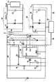
本発明に係るDC−DCコンバータの一実施形態例を図1に示す。この実施形態例のDC−DCコンバータは、前記図4に示す構成に加えて、シリーズレギュレータ18を有している。この実施形態例のDC−DCコンバータにおいて、シリーズレギュレータ18に関する構成以外の構成は図4に示す構成とほぼ同様である。この実施形態例では、図4に示す回路と同一構成部分には同一符号を付し、その共通部分の重複説明は省略する。
【0026】
シリーズレギュレータ18は、補助整流平滑回路29の出力部と、PWM制御IC4の電源端子Vccとを接続する制御電源供給路30に介設されている。このシリーズレギュレータ18は、補助整流平滑回路29から出力される電圧V29を利用してPWM制御IC4の設定の電源電圧を生成し当該電圧をPWM制御IC4の電源端子Vccに供給する構成を有する。このため、補助整流平滑回路29の出力電圧V29が上昇しても、シリーズレギュレータ18からは設定の電源電圧がPWM制御IC4の電源端子Vccに供給されるので、補助整流平滑回路29の出力電圧V29の上昇に起因して耐圧上限電圧よりも高い電源電圧がPWM制御IC4に加えられる事態を防止することができる。
【0027】
また、シリーズレギュレータ18の出力電圧は、ラッチ回路25のラッチ停止動作に関与するNチャネルMOSFET5のソースに加えられる構成となっている。シリーズレギュレータ18は、補助整流平滑回路29の出力電圧V29が設定の電源電圧Vcc以下に低下すると、シリーズレギュレータ18の出力電圧が、出力電圧V29の低下に応じて低下していく構成である。このため、ラッチ回路25は、出力用整流平滑回路28の出力電圧Voutが低電圧保護動作が必要な程度に低下したときには、その出力電圧Voutの低下に伴った補助整流平滑回路29の出力電圧V29の低下をシリーズレギュレータ18の出力電圧により検知することができて、ラッチ停止動作を行うことができる。
【0028】
なお、本発明はこの実施形態例の構成に限定されるものではなく、様々な実施の形態を取り得る。例えば、実施形態例では、補助整流平滑回路29は、トランス2の補助コイル2cに接続し当該補助コイル2cの出力電圧を整流平滑する回路構成であったが、例えば、出力用整流平滑回路28のチョークコイル11に二次コイルを設け、補助整流平滑回路29は、そのチョークコイル11の二次コイルに接続して、主スイッチ3のオフ期間におけるその二次コイルの出力電圧をピーク整流し、平滑する回路構成としてもよい。この場合にも、出力用整流平滑回路28の出力電圧Voutにほぼ比例した電圧を補助整流平滑回路29から出力させることができる。
【0029】
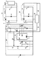
また、実施形態例では、ラッチ回路25は、シリーズレギュレータ18の出力電圧を利用して、ラッチ停止動作を行う構成であったが、例えば、図2に示すように、補助整流平滑回路29の出力部と、ラッチ停止動作に関わるNチャネルMOSFET5のソースとを直接的に接続し、ラッチ回路25は、直接的に検出された補助整流平滑回路29の出力電圧V29に基づいてラッチ停止動作を行う構成としてもよい。この場合には、シリーズレギュレータ18の出力電圧はPWM制御IC4の電源電圧専用の電圧となる。
【0030】
さらに、主スイッチ3のオフ期間における補助整流平滑回路29のチョークコイル16の電圧をピーク整流した電圧は、補助整流平滑回路29の出力電圧V29とほぼ等しい電圧となる。このことから、例えば、主スイッチ3のオフ期間における補助整流平滑回路29のチョークコイル16の電圧をピーク整流する回路を設け、ラッチ回路25は、そのピーク整流回路を介して補助整流平滑回路29の出力電圧V29を間接的に検出し、当該検出電圧に基づいてラッチ停止動作を行う構成としてもよい。
【0031】
ラッチ回路25は、補助整流平滑回路29の出力電圧V29をシリーズレギュレータ18を介して検出するのではなく、補助整流平滑回路29の出力電圧V29をそれ以外の手段により間接的に検出し、あるいは、直接的に検出し、当該検出電圧に基づいて、ラッチ停止動作を行う構成としてもよい。
【0032】
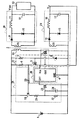
さらに、例えば、図3に示されるように、主スイッチ3のスイッチング動作を停止させるための指令信号を外部から入力するための外部制御用の端子31を設け、外部から外部制御用の端子31を介して主スイッチ3のスイッチング動作停止の指令信号をDC−DCコンバータに加えることを可能にする構成を設けてもよい。この場合には、ラッチ停止阻止回路32を設けることが好ましい。このラッチ停止阻止回路32は、外部から外部制御用の端子31を介して主スイッチ3のスイッチング動作停止の指令信号が加えられたことを検知したときには、その指令に従った主スイッチ3のスイッチング動作停止によって出力用整流平滑回路28の出力電圧Voutが低下してもラッチ回路25にラッチ停止動作を行わせない構成を有しているものである。
【0033】
さらに、例えば、図3の鎖線に示すように、入力電源低下時スイッチング停止回路33を設けてもよい。この入力電源低下時スイッチング停止回路33は、直流入力電源1から入力した電圧を検出し当該検出電圧が設定の電圧よりも低下したことを検知したときには主スイッチ3のスイッチング動作を停止させる構成を有するものである。この入力電源低下時スイッチング停止回路33が設けられる場合にも、上記同様のラッチ停止阻止回路32を設けることが好ましい。つまり、この場合には、ラッチ停止阻止回路32は、入力電源低下時スイッチング停止回路33により主スイッチ3のスイッチング動作が停止したことを検知したときには、その主スイッチ3のスイッチング動作停止によって出力用整流平滑回路28の出力電圧Voutが低下してもラッチ回路25にラッチ停止動作を行わせない構成を有しているものである。
【0034】
さらに、実施形態例では、DC−DCコンバータはフォワードコンバータ方式のものであったが、本発明は、例えば、フライバックコンバータ方式等の他の電力変換回路方式のDC−DCコンバータにも適用可能である。
【0035】
【発明の効果】
この発明によれば、補助整流平滑回路と制御回路を接続する制御電源供給路にシリーズレギュレータを介設した。このため、負荷短絡などに起因して出力用整流平滑回路の出力電圧と、補助整流平滑回路の出力電圧との比例関係が崩れて補助整流平滑回路の出力電圧が異常上昇しても、シリーズレギュレータから制御回路へは設定の電源電圧が供給される。これにより、制御回路に入力する電源電圧に対する制御回路の電圧ディレーティングを確保し易くなる。
【0036】
また、シリーズレギュレータによって、制御回路に入力する電源電圧が設定値よりも上昇する変動が抑制されるので、例えば、電源電圧の設定値を今までよりも制御回路の耐圧上限電圧に近い電圧に設定しても、制御回路に耐圧上限電圧を超えた大きな電源電圧が加えられる事態を回避することができる。このため、電源電圧の設定値を制御回路の耐圧上限電圧の近傍の従来よりも高めの電圧に設定することによって、電源電圧の設定値と、ラッチ回路がラッチ停止を行うときの低電圧保護動作用の設定電圧との電圧差を広げることができる。これにより、電源電圧が正常な範囲内での降下変動であったのにラッチ回路がラッチ停止動作を行ってしまったという低電圧保護動作の誤動作を防止することができる。よって、低電圧保護動作に対する信頼性を高めることができる。
【0037】
特に、主スイッチのスイッチング制御の精度を高めるために、高精度な低耐圧の制御回路が使用される場合があるが、この場合には、電源電圧の設定値と低電圧保護動作用の設定電圧との電圧差が小さくなるので、低電圧保護動作の誤動作が発生し易く問題であったが、この発明の特有な構成を備えることによって、その問題を容易に解決することができる。このことから、この発明の特有な構成は、低耐圧の制御回路が使用される場合に非常に有効である。
【0038】
ところで、出力用整流平滑回路の出力電圧を直接的に検出して低電圧保護動作を行おうとすると、フォトカプラを使用することになる。フォトカプラは、寿命が限られており、かつ高温の環境下で使用できないという欠点がある。これに対して、この発明では、出力用整流平滑回路の出力電圧を補助整流平滑回路を利用して間接的に検出し、この検出電圧に基づいて低電圧保護動作を行う構成であり、フォトカプラを使用しない。このため、フォトカプラに起因した問題発生を抑制することができて、DC−DCコンバータの高信頼性化を実現できる。
【0039】
低電圧保護動作を行うラッチ回路は、補助整流平滑回路の出力電圧を直接的に検出して当該検出電圧に基づいてラッチ停止動作を行う構成である場合にも、補助整流平滑回路の出力電圧をシリーズレギュレータを介して間接的に検出し当該検出電圧に基づいてラッチ停止動作を行う構成である場合にも、同様のラッチ停止動作を行うことができる。補助整流平滑回路の出力部からラッチ回路に取り込まれる検出電圧の検出方式によらずに、本発明に特有な構成を備えることによって上記同様の優れた効果を奏することができる。
【0040】
外部制御用の端子が設けられると共に、ラッチ停止阻止回路が設けられているものにあっては、ラッチ停止阻止回路によりラッチ停止することを回避しながら、DC−DCコンバータの外部から動作制御を可能にする効果がある。
【0041】
入力電源低下時スイッチング停止回路が設けられると共に、ラッチ停止阻止回路が設けられているものにあっては、入力電源低下時スイッチング停止回路によって、外部からDC−DCコンバータに供給される入力電圧が設定の電圧よりも低下した場合には主スイッチのスイッチング動作が停止してDC−DCコンバータの動作を停止させることができる。その上、そのように入力電圧の異常により主スイッチのスイッチング動作が停止した場合には、ラッチ停止阻止回路によってラッチ停止を阻止できるので、入力電圧回復後の再起動が容易となる。
【図面の簡単な説明】
【図1】本発明に係るDC−DCコンバータの一実施形態例を示す回路図である。
【図2】その他の実施形態例を示す回路図である。
【図3】さらに、その他の実施形態例を示す回路図である。
【図4】従来のDC−DCコンバータの一例を示す回路図である。
【符号の説明】
1 直流入力電源
2 トランス
3 主スイッチ
4 PWM制御IC
5,23 NチャネルMOSFET
6,7,20,21,22 抵抗体
8 ツェナーダイオード
9,10,14,15 ダイオード
11,16 チョークコイル
12,17,24 コンデンサ
13 負荷装置 18 シリーズレギュレータ
19 PNPトランジスタ
25 ラッチ回路
26 PWM変調部
27 起動回路
28 出力用整流平滑回路
29 補助整流平滑回路[0001]
TECHNICAL FIELD OF THE INVENTION
The present invention relates to an isolated DC-DC converter.
[0002]
[Background Art]
FIG. 4 shows an example of a circuit configuration of the DC-DC converter. The DC-DC converter shown in FIG. 4 is a forward converter, and is disclosed in Patent Document 1 (Japanese Patent Application Laid-Open No. 2001-161062).
[0003]
The DC-DC converter shown in FIG. 4 includes a transformer 2, a latch circuit 25, a PWM modulation unit 26, a start-up circuit 27, an output rectifying / smoothing circuit 28, and an auxiliary rectifying / smoothing circuit 29. ing.
[0004]
In addition, the transformer 2 includes a primary coil 2a, a secondary coil 2b, and an auxiliary coil 2c. The latch circuit 25 includes a PNP transistor 19, resistors 20, 21 and 22, an N-channel MOSFET 23, and a capacitor 24. The PWM modulator 26 includes a main switch 3 and a PWM control IC 4 that is a control circuit for controlling the switching operation of the main switch 3. The PWM control IC 4 includes a power supply terminal Vcc, a gate drive pulse output It has a terminal OUT, an operation control input terminal OFF, and a ground terminal GND. The starting circuit 27 includes the N-channel MOSFET 5, the resistors 6, 7, and the Zener diode 8. The output rectifying / smoothing circuit 28 includes diodes 9 and 10, a choke coil 11, and a capacitor 12. The auxiliary rectifying / smoothing circuit 29 includes the diodes 14 and 15, the choke coil 16, and the capacitor 17.
[0005]
An operation example of the DC-DC converter will be described. For example, an ON signal for turning on the main switch 3 and an OFF signal for turning off the main switch 3 are alternately output from the gate drive pulse output terminal OUT of the PWM control IC 4 to the main switch 3. The main switch 3 performs an ON / OFF switching operation based on the ON signal and the OFF signal. By the switching operation of the main switch 3, the DC voltage input from the external DC input power supply 1 is converted into an AC voltage on the primary coil 2 a side of the transformer 2 and transmitted to the secondary coil 2 b side of the transformer 2. The output rectifying / smoothing circuit 28 rectifies and smoothes the AC voltage output from the secondary coil 2b of the transformer 2 and converts it into a DC voltage. This DC voltage Vout is supplied to an external load device 13 connected to a DC-DC converter. A signal corresponding to the output voltage Vout is transmitted to the PWM control IC 4 as a feedback signal by a feedback loop (not shown). Based on the feedback signal, the PWM control IC 4 controls the switching operation of the main switch 3 by the PWM control method, so that the DC voltage Vout supplied to the load device 13 is stabilized.
[0006]
Since the auxiliary rectifying / smoothing circuit 29 has the same choke input rectification type circuit configuration as the output rectifying / smoothing circuit 28, both the choke coil 11 of the output rectifying / smoothing circuit 28 and the choke coil 16 of the auxiliary rectifying / smoothing circuit 29 are in the continuous current mode. Is operating, the DC voltage V output from the auxiliary rectifying and smoothing circuit 29 is 29 Is substantially proportional to the output voltage Vout. Therefore, the DC voltage Vout is controlled by the stabilization control of the output voltage Vout by the PWM control IC 4. 29 Is also almost stabilized. This DC voltage V 29 Is supplied to the power supply terminal Vcc of the PWM control IC 4 as the power supply voltage of the PWM control IC 4. When the output voltage Vout decreases due to a load short circuit or the like, the DC voltage Vout 29 Also decrease almost in proportion.
[0007]
The start-up circuit 27 is driven when the power supply voltage is not supplied from the auxiliary rectifying / smoothing circuit 29 to the power supply terminal Vcc of the PWM control IC 4 or when the power supply voltage is extremely low, for example, at the time of start-up or when a load is short-circuited. Circuit. That is, in the start-up circuit 27, the gate of the N-channel MOSFET 5 is connected to the cathode of the Zener diode 8, and a current flows from the DC input power supply 1 to the Zener diode 8 via the resistor 7, so that the N-channel MOSFET 5 The gate voltage is fixed at the Zener voltage with respect to the ground. The source of the N-channel MOSFET 5 is connected to the output of the auxiliary rectifying / smoothing circuit 29, and the DC voltage V output from the auxiliary rectifying / smoothing circuit 29 is connected to the source of the N-channel MOSFET 5. 29 Is applied.
[0008]
For example, the DC voltage V 29 Is not output, or DC voltage V 29 Is very low or the DC voltage V 29 DC voltage V 29 When the difference between the threshold voltage and the Zener voltage (that is, the voltage between the gate and the source of the N-channel MOSFET 5) has spread beyond the threshold voltage, the N-channel MOSFET 5 conducts. As a result, a current flows from the DC input power supply 1 to the power supply terminal Vcc of the PWM control IC 4 via the resistor 6.
[0009]
In the normal operation of the DC-DC converter, the N-channel MOSFET 5 is turned off, and the power supply voltage is supplied from the auxiliary rectifying / smoothing circuit 29 to the power supply terminal Vcc of the PWM control IC 4. As described above, when the voltage supplied from the auxiliary rectifying / smoothing circuit 29 to the power supply terminal Vcc of the PWM control IC 4 is zero or very low, as described above, the N-channel MOSFET 5 of the starting circuit 27 conducts, The starting circuit 27 supplies a voltage based on the input DC power supply 1 to the power supply terminal Vcc of the PWM control IC 4 as a power supply voltage.
[0010]
The latch circuit 25 performs a low-voltage protection operation, and is in a state where the N-channel MOSFET 5 is conducting (that is, the output voltage V of the auxiliary rectifying / smoothing circuit 29). 29 Is lower than the set voltage for the low-voltage protection operation) for a certain period or more, the DC-DC converter stops latching. That is, when the N-channel MOSFET 5 conducts, a voltage is generated across the resistor 6, a base current flows to the PNP transistor 19 via the resistor 20, and the PNP transistor 19 is turned on. When the PNP transistor 19 is turned on, a current flows from the DC input power supply 1 to the capacitor 24 via the resistor 21, and the capacitor 24 is charged according to a time constant determined by the resistor 21 and the capacitor 24. Since the charging voltage of the capacitor 24 is applied to the gate of the N-channel MOSFET 23, when the charging voltage of the capacitor 24 reaches the threshold voltage of the N-channel MOSFET 23, the N-channel MOSFET 23 turns on. As a result, the voltage of the operation control input terminal OFF of the PWM control IC 4 becomes low level.
[0011]
When the voltage of the operation control input terminal OFF becomes low level, the output of the ON signal (gate drive pulse) from the PWM control IC 4 to the main switch 3 stops. Due to the stop of the output of the ON signal, the main switch 3 remains off, and the voltage Vout output from the DC-DC converter to the load device 13 decreases. The voltage V output from the auxiliary rectifying / smoothing circuit 29 29 , Similarly to the output voltage Vout, the conduction state of the N-channel MOSFET 5 of the starting circuit 27 is maintained. As a result, the ON state of the PNP transistor 19 and the N-channel MOSFET 23 is maintained, and the latch of the DC-DC converter stops.
[0012]
Note that the PNP transistor 19 is also turned on at the time of start-up, but the time constant of the resistor 21 and the capacitor 24 is set longer than the time until the start-up operation is completed. Absent. On the other hand, when the load short-circuit state continues longer than the time constant of the resistor 21 and the capacitor 24, the latch circuit 25 stops latching the DC-DC converter as described above.
[0013]
[Patent Document 1]
JP 2001-161062A
[0014]
[Problems to be solved by the invention]
When the voltage Vout output from the output rectifying / smoothing circuit 28 decreases due to, for example, a load short circuit, the decrease in the output voltage Vout is transmitted to the PWM control IC 4 by a feedback loop (not shown), and the PWM control IC 4 Thus, switching control of the main switch 3 is performed to compensate for a decrease in the output voltage Vout. As a result, the output voltage Vout rises and attempts to stabilize at the set voltage.
[0015]
At this time, even if a load short circuit occurs, the output voltage V of the auxiliary rectifying / smoothing circuit 29 caused by the load short circuit. 29 (In other words, when the load is short-circuited, the output voltage Vout of the output rectifying / smoothing circuit 28 and the output voltage V 29 When the switching operation of the main switch 3 is performed to compensate for the decrease in the output voltage Vout, the output voltage of the auxiliary coil 2c increases. As a result, the output voltage V of the auxiliary rectifying and smoothing circuit 29 29 Occurs. In recent years, it has been required to increase the output voltage Vout. If the component constants and the like are designed to meet this demand, the auxiliary rectifying / smoothing circuit 29 at the time of load short-circuiting as described above is caused by this. Output voltage V 29 The upward trend of the increase.
[0016]
Incidentally, the PWM control IC having a low withstand voltage (that is, the PWM control IC having a small difference between the voltage level of the ON signal output from the PWM control IC to the main switch and the withstand voltage upper limit voltage of the PWM control IC) is higher. The accuracy of the switching control of the main switch is better than that of the withstand voltage. For this reason, a low withstand voltage device may be used as the PWM control IC 4 in some cases. The use of this low withstand voltage PWM control IC and the output voltage V of the auxiliary rectifying / smoothing circuit 29 when a load short circuit occurs due to the recent increase in voltage. 29 The following problems are coming to the fore due to the large upward trend of the data.
[0017]
That is, the output voltage Vout of the output rectifying / smoothing circuit 28 and the output voltage V 29 And the output voltage V 29 Becomes uncontrolled and the output voltage V 29 Has risen unnecessarily, since the withstand voltage of the PWM control IC 4 is low, the large output voltage V 29 There is a problem that voltage derating of the PWM control IC 4 cannot be ensured with respect to (power supply voltage). Also, the power supply voltage V 29 However, there is a problem that a situation in which the voltage exceeds the withstand voltage upper limit voltage of the PWM control IC 4 easily occurs.
[0018]
To solve this problem, a PWM control IC with a high withstand voltage may be used. However, the accuracy of the switching control of the main switch 3 is lower than that of a PWM control IC with a low withstand voltage.
[0019]
Further, the following problem also occurs. That is, in the DC-DC converter of FIG. 29 Is supplied to the PWM control IC 4 as a power supply voltage and supplied to the latch circuit 25 as a detection voltage of the output voltage Vout. The latch circuit 25 outputs the output voltage V 29 Performs a latch stop operation based on The voltage level of the ON signal applied from the PWM control IC 4 to the main switch 3 is the same as the power supply voltage supplied to the PWM control IC 4. Further, the threshold value of the main switch 3 tends to increase as the environmental temperature decreases. From these facts, the voltage at which the latch circuit 25 performs the low-voltage protection operation (that is, the set voltage for the low-voltage protection operation) is set so that the DC-DC converter can be reliably started even in a low-temperature environment. It is necessary to set the threshold to a value higher than the threshold value of the main switch 3 in a low temperature environment.
[0020]
In this case, since the withstand voltage upper limit voltage of the PWM control IC 4 is low, the voltage difference between the withstand voltage upper limit voltage of the PWM control IC 4 and the set voltage for the low voltage protection operation becomes small. The set value of the power supply voltage input to the PWM control IC 4 is determined within the voltage range from the set voltage for the low-voltage protection operation to the withstand voltage upper limit voltage of the PWM control IC 4. When the voltage difference from the set voltage for the voltage protection operation is reduced, the voltage difference between the power supply voltage set in the PWM control IC 4 and the withstand voltage upper limit voltage, and the power supply voltage set in the PWM control IC 4 and the low voltage protection operation are inevitably increased. The voltage difference from the set voltage for use becomes smaller. For this reason, the power supply voltage V input to the PWM control IC 4 29 Varies within the range considered normal, the power supply voltage V 29 Exceeds the withstand voltage upper limit voltage of the PWM control IC 4 or the power supply voltage V 29 May lower than the set voltage for the low-voltage protection operation, the latch circuit 25 operates, and the DC-DC converter stops latching, which may cause a malfunction of the low-voltage protection operation.
[0021]
In order to solve this problem, by increasing the withstand voltage upper limit voltage of the PWM control IC 4 by using a high withstand voltage PWM control IC, the voltage between the withstand voltage upper limit voltage of the PWM control IC 4 and the set voltage for the low voltage protection operation is increased. Although it is conceivable to widen the voltage difference, the accuracy of the switching control of the main switch 3 is deteriorated as compared with the case where a low-breakdown-voltage PWM control IC is used.
[0022]
SUMMARY OF THE INVENTION The present invention has been made to solve the above-described problems, and an object of the present invention is to improve the reliability of low-voltage protection operation while improving the accuracy of switching control of a main switch by using a low-voltage control circuit. It is another object of the present invention to provide a DC-DC converter.
[0023]
[Means for Solving the Problems]
In order to achieve the above object, the present invention provides means for solving the above problems with the following configuration. That is, according to the present invention, an AC power is output from a secondary side of a transformer by a switching operation of a main switch provided on a primary side of the transformer, and the AC power is output to a rectifying and smoothing rectifier connected to a secondary side of the transformer. In a DC-DC converter having a configuration to be converted to DC by a circuit, a control circuit for controlling a switching operation of a main switch and an auxiliary for rectifying and smoothing AC output power of an auxiliary coil provided in a transformer to convert to DC. A rectifying / smoothing circuit, a control power supply path connecting the output section of the auxiliary rectifying / smoothing circuit to the control circuit, and detecting the output voltage of the auxiliary rectifying / smoothing circuit as an output voltage of the output rectifying / smoothing circuit, and detecting the detected voltage. When detecting that the voltage has dropped below the set voltage for the low-voltage protection operation, the switching operation of the main switch is stopped and the DC-DC converter is activated. And a latch circuit for stopping the latching. The control power supply path generates a power supply voltage set by the control circuit using the voltage output from the auxiliary rectifying / smoothing circuit and supplies the power supply voltage to the control circuit. A series regulator is provided to prevent a situation in which a power supply voltage higher than the withstand voltage upper limit voltage of the control circuit is supplied to the control circuit due to a rise in the output voltage of the auxiliary rectifying / smoothing circuit. I have.
[0024]
BEST MODE FOR CARRYING OUT THE INVENTION
Hereinafter, embodiments of the present invention will be described with reference to the drawings.
[0025]
FIG. 1 shows an embodiment of a DC-DC converter according to the present invention. The DC-DC converter of this embodiment has a series regulator 18 in addition to the configuration shown in FIG. In the DC-DC converter of this embodiment, the configuration other than the configuration related to the series regulator 18 is almost the same as the configuration shown in FIG. In this embodiment, the same components as those of the circuit shown in FIG. 4 are denoted by the same reference numerals, and redundant description of the common portions will be omitted.
[0026]
The series regulator 18 is provided on a control power supply path 30 that connects the output of the auxiliary rectifying and smoothing circuit 29 and the power supply terminal Vcc of the PWM control IC 4. The series regulator 18 controls the voltage V output from the auxiliary rectifying / smoothing circuit 29. 29 , A power supply voltage set for the PWM control IC 4 is generated, and the voltage is supplied to the power supply terminal Vcc of the PWM control IC 4. Therefore, the output voltage V of the auxiliary rectifying and smoothing circuit 29 is 29 Rises, the set power supply voltage is supplied from the series regulator 18 to the power supply terminal Vcc of the PWM control IC 4, so that the output voltage V 29 Can be prevented from being applied to the PWM control IC 4 due to a rise in the power supply voltage higher than the withstand voltage upper limit voltage.
[0027]
The output voltage of the series regulator 18 is applied to the source of the N-channel MOSFET 5 involved in the latch stop operation of the latch circuit 25. The series regulator 18 outputs the output voltage V 29 Falls below the set power supply voltage Vcc, the output voltage of the series regulator 18 changes to the output voltage Vcc. 29 Is reduced in accordance with the decrease in For this reason, when the output voltage Vout of the output rectifying / smoothing circuit 28 decreases to such an extent that the low-voltage protection operation is required, the latch circuit 25 outputs the output voltage Vout of the auxiliary rectifying / smoothing circuit 29 with the decrease of the output voltage Vout. 29 Can be detected by the output voltage of the series regulator 18, and the latch stop operation can be performed.
[0028]
It should be noted that the present invention is not limited to the configuration of this embodiment, but can take various embodiments. For example, in the embodiment, the auxiliary rectifying / smoothing circuit 29 is connected to the auxiliary coil 2c of the transformer 2 and rectifies and smoothes the output voltage of the auxiliary coil 2c. The choke coil 11 is provided with a secondary coil, and the auxiliary rectifying / smoothing circuit 29 is connected to the secondary coil of the choke coil 11 to perform peak rectification on the output voltage of the secondary coil during the OFF period of the main switch 3 to smooth the output voltage. The circuit configuration may be as follows. Also in this case, a voltage substantially proportional to the output voltage Vout of the output rectifying / smoothing circuit 28 can be output from the auxiliary rectifying / smoothing circuit 29.
[0029]
In the embodiment, the latch circuit 25 performs the latch stop operation by using the output voltage of the series regulator 18. However, for example, as shown in FIG. Unit and the source of the N-channel MOSFET 5 involved in the latch stop operation are directly connected, and the latch circuit 25 outputs the output voltage V of the auxiliary rectifying / smoothing circuit 29 directly detected. 29 The latch stop operation may be performed based on In this case, the output voltage of the series regulator 18 is a voltage dedicated to the power supply voltage of the PWM control IC 4.
[0030]
Further, the voltage obtained by peak-rectifying the voltage of the choke coil 16 of the auxiliary rectifying / smoothing circuit 29 during the OFF period of the main switch 3 is the output voltage V of the auxiliary rectifying / smoothing circuit 29. 29 Is almost equal to For this reason, for example, a circuit for peak rectifying the voltage of the choke coil 16 of the auxiliary rectifying / smoothing circuit 29 during the OFF period of the main switch 3 is provided, and the latch circuit 25 is connected to the auxiliary rectifying / smoothing circuit 29 via the peak rectifying circuit. Output voltage V 29 May be detected indirectly and a latch stop operation is performed based on the detected voltage.
[0031]
The latch circuit 25 outputs the output voltage V 29 Is detected via the series regulator 18, and the output voltage V 29 May be detected indirectly by other means or directly, and the latch stop operation may be performed based on the detected voltage.
[0032]
Further, for example, as shown in FIG. 3, an external control terminal 31 for externally inputting a command signal for stopping the switching operation of the main switch 3 is provided, and the external control terminal 31 is externally provided. A configuration may be provided that allows a command signal to stop the switching operation of the main switch 3 to be applied to the DC-DC converter via the DC-DC converter. In this case, it is preferable to provide the latch stop prevention circuit 32. When detecting that a command signal for stopping the switching operation of the main switch 3 is applied from outside via the external control terminal 31, the latch stop prevention circuit 32 performs the switching operation of the main switch 3 according to the command. Even if the output voltage Vout of the output rectifying / smoothing circuit 28 decreases due to the stop, the latch circuit 25 is not allowed to perform the latch stop operation.
[0033]
Further, for example, as shown by the chain line in FIG. The input power supply drop switching stop circuit 33 detects the voltage input from the DC input power supply 1 and stops the switching operation of the main switch 3 when it detects that the detected voltage has dropped below a set voltage. Things. Even when the input power supply drop switching stop circuit 33 is provided, it is preferable to provide the same latch stop prevention circuit 32 as described above. In other words, in this case, when the latch stop prevention circuit 32 detects that the switching operation of the main switch 3 is stopped by the switching stop circuit 33 when the input power supply drops, the latch rectification for output is performed by stopping the switching operation of the main switch 3. Even if the output voltage Vout of the smoothing circuit 28 decreases, the latch circuit 25 does not perform the latch stop operation.
[0034]
Further, in the embodiment, the DC-DC converter is of the forward converter type. However, the present invention is applicable to a DC-DC converter of another power conversion circuit type such as a flyback converter type. is there.
[0035]
【The invention's effect】
According to the present invention, the series regulator is provided in the control power supply path connecting the auxiliary rectifying / smoothing circuit and the control circuit. Therefore, even if the output voltage of the auxiliary rectifying / smoothing circuit is abnormally increased due to the output voltage of the auxiliary rectifying / smoothing circuit and the output voltage of the auxiliary rectifying / smoothing circuit being broken due to a load short circuit, etc. Supplies a set power supply voltage to the control circuit. This makes it easier to ensure voltage derating of the control circuit with respect to the power supply voltage input to the control circuit.
[0036]
In addition, the series regulator suppresses fluctuations in which the power supply voltage input to the control circuit rises above the set value. Even in this case, a situation in which a large power supply voltage exceeding the withstand voltage upper limit voltage is applied to the control circuit can be avoided. Therefore, by setting the set value of the power supply voltage to a voltage higher than the conventional voltage near the withstand voltage upper limit voltage of the control circuit, the set value of the power supply voltage and the low voltage protection operation when the latch circuit stops latching. The voltage difference from the set voltage for use can be widened. Thus, it is possible to prevent a malfunction of the low-voltage protection operation in which the latch circuit performs the latch stop operation even when the power supply voltage has a drop fluctuation within a normal range. Therefore, reliability for the low-voltage protection operation can be improved.
[0037]
In particular, in order to increase the switching control accuracy of the main switch, a high-precision low-voltage control circuit may be used. In this case, the set value of the power supply voltage and the set voltage for the low-voltage protection operation are used. However, since the voltage difference between the low-voltage protection operation and the low-voltage protection operation is small, the low-voltage protection operation is likely to malfunction. However, the provision of the unique configuration of the present invention can easily solve the problem. For this reason, the unique configuration of the present invention is very effective when a low-breakdown-voltage control circuit is used.
[0038]
By the way, if the output voltage of the output rectifying / smoothing circuit is directly detected to perform the low-voltage protection operation, a photocoupler will be used. Photocouplers have the disadvantage that they have a limited life and cannot be used in a high-temperature environment. On the other hand, in the present invention, the output voltage of the output rectifying / smoothing circuit is indirectly detected by using the auxiliary rectifying / smoothing circuit, and the low voltage protection operation is performed based on the detected voltage. Do not use For this reason, it is possible to suppress the occurrence of a problem caused by the photocoupler, and to achieve high reliability of the DC-DC converter.
[0039]
The latch circuit that performs the low-voltage protection operation also detects the output voltage of the auxiliary rectifying / smoothing circuit directly and performs the latch stop operation based on the detected voltage. A similar latch stop operation can be performed even when the latch stop operation is performed indirectly through a series regulator and the latch stop operation is performed based on the detected voltage. The same excellent effects as described above can be obtained by providing a configuration unique to the present invention, regardless of the method of detecting the detection voltage taken into the latch circuit from the output section of the auxiliary rectifying / smoothing circuit.
[0040]
In the case where an external control terminal is provided and a latch stop prevention circuit is provided, the operation can be controlled from outside the DC-DC converter while preventing the latch stop by the latch stop prevention circuit. Has the effect of
[0041]
In the case where a switching stop circuit is provided when the input power supply drops and a latch stop prevention circuit is provided, the input voltage supplied from the outside to the DC-DC converter is set by the switching stop circuit when the input power supply drops. When the voltage drops below the threshold voltage, the switching operation of the main switch is stopped, and the operation of the DC-DC converter can be stopped. In addition, when the switching operation of the main switch is stopped due to the abnormality of the input voltage, the latch stop can be prevented by the latch stop prevention circuit, so that the restart after the input voltage recovery is facilitated.
[Brief description of the drawings]
FIG. 1 is a circuit diagram showing an embodiment of a DC-DC converter according to the present invention.
FIG. 2 is a circuit diagram showing another embodiment.
FIG. 3 is a circuit diagram showing still another embodiment.
FIG. 4 is a circuit diagram showing an example of a conventional DC-DC converter.
[Explanation of symbols]
1 DC input power supply
2 transformer
3 Main switch
4 PWM control IC
5,23 N-channel MOSFET
6,7,20,21,22 Resistor
8 Zener diode
9,10,14,15 Diode
11,16 Choke coil
12, 17, 24 capacitors
13 Load device 18 Series regulator
19 PNP transistor
25 Latch circuit
26 PWM modulator
27 Startup circuit
28 Rectifying smoothing circuit for output
29 Auxiliary rectification smoothing circuit