JP2004166312A - Improved reclocker and router cell - Google Patents
Improved reclocker and router cell Download PDFInfo
- Publication number
- JP2004166312A JP2004166312A JP2004050546A JP2004050546A JP2004166312A JP 2004166312 A JP2004166312 A JP 2004166312A JP 2004050546 A JP2004050546 A JP 2004050546A JP 2004050546 A JP2004050546 A JP 2004050546A JP 2004166312 A JP2004166312 A JP 2004166312A
- Authority
- JP
- Japan
- Prior art keywords
- router
- output
- input
- reclocker
- signal
- Prior art date
- Legal status (The legal status is an assumption and is not a legal conclusion. Google has not performed a legal analysis and makes no representation as to the accuracy of the status listed.)
- Pending
Links
- 239000011159 matrix material Substances 0.000 abstract description 69
- 238000010586 diagram Methods 0.000 description 17
- 238000013461 design Methods 0.000 description 9
- 238000000034 method Methods 0.000 description 3
- 238000012545 processing Methods 0.000 description 2
- 238000009825 accumulation Methods 0.000 description 1
- 230000003321 amplification Effects 0.000 description 1
- 238000004891 communication Methods 0.000 description 1
- 238000000605 extraction Methods 0.000 description 1
- 238000012986 modification Methods 0.000 description 1
- 230000004048 modification Effects 0.000 description 1
- 238000003199 nucleic acid amplification method Methods 0.000 description 1
- 238000006467 substitution reaction Methods 0.000 description 1
Images
Classifications
-
- H—ELECTRICITY
- H04—ELECTRIC COMMUNICATION TECHNIQUE
- H04Q—SELECTING
- H04Q3/00—Selecting arrangements
- H04Q3/64—Distributing or queueing
- H04Q3/66—Traffic distributors
- H04Q3/665—Circuit arrangements therefor
-
- H—ELECTRICITY
- H04—ELECTRIC COMMUNICATION TECHNIQUE
- H04N—PICTORIAL COMMUNICATION, e.g. TELEVISION
- H04N5/00—Details of television systems
- H04N5/222—Studio circuitry; Studio devices; Studio equipment
- H04N5/262—Studio circuits, e.g. for mixing, switching-over, change of character of image, other special effects ; Cameras specially adapted for the electronic generation of special effects
- H04N5/268—Signal distribution or switching
-
- H—ELECTRICITY
- H04—ELECTRIC COMMUNICATION TECHNIQUE
- H04Q—SELECTING
- H04Q2213/00—Indexing scheme relating to selecting arrangements in general and for multiplex systems
- H04Q2213/13166—Fault prevention
-
- H—ELECTRICITY
- H04—ELECTRIC COMMUNICATION TECHNIQUE
- H04Q—SELECTING
- H04Q2213/00—Indexing scheme relating to selecting arrangements in general and for multiplex systems
- H04Q2213/13196—Connection circuit/link/trunk/junction, bridge, router, gateway
-
- H—ELECTRICITY
- H04—ELECTRIC COMMUNICATION TECHNIQUE
- H04Q—SELECTING
- H04Q2213/00—Indexing scheme relating to selecting arrangements in general and for multiplex systems
- H04Q2213/13214—Clock signals
-
- H—ELECTRICITY
- H04—ELECTRIC COMMUNICATION TECHNIQUE
- H04Q—SELECTING
- H04Q2213/00—Indexing scheme relating to selecting arrangements in general and for multiplex systems
- H04Q2213/13292—Time division multiplexing, TDM
-
- H—ELECTRICITY
- H04—ELECTRIC COMMUNICATION TECHNIQUE
- H04Q—SELECTING
- H04Q2213/00—Indexing scheme relating to selecting arrangements in general and for multiplex systems
- H04Q2213/1332—Logic circuits
-
- H—ELECTRICITY
- H04—ELECTRIC COMMUNICATION TECHNIQUE
- H04Q—SELECTING
- H04Q2213/00—Indexing scheme relating to selecting arrangements in general and for multiplex systems
- H04Q2213/13322—Integrated circuits
-
- H—ELECTRICITY
- H04—ELECTRIC COMMUNICATION TECHNIQUE
- H04Q—SELECTING
- H04Q2213/00—Indexing scheme relating to selecting arrangements in general and for multiplex systems
- H04Q2213/1334—Configuration within the switch
-
- H—ELECTRICITY
- H04—ELECTRIC COMMUNICATION TECHNIQUE
- H04Q—SELECTING
- H04Q2213/00—Indexing scheme relating to selecting arrangements in general and for multiplex systems
- H04Q2213/1336—Synchronisation
Landscapes
- Engineering & Computer Science (AREA)
- Multimedia (AREA)
- Signal Processing (AREA)
- Computer Networks & Wireless Communication (AREA)
- Data Exchanges In Wide-Area Networks (AREA)
- Synchronisation In Digital Transmission Systems (AREA)
- Use Of Switch Circuits For Exchanges And Methods Of Control Of Multiplex Exchanges (AREA)
- Studio Circuits (AREA)
- Electronic Switches (AREA)
Abstract
Description
本特許出願は、信号切換およびルーティングの分野に関する。より詳細には、本出願は、複数の相互接続されたルータセルを含む大型ルータマトリクスにおいて、映像信号、電気通信信号、または他の種類の時間感受性信号の切換えおよびルーティングを行う際に特に有用な、改良されたリクロッカ回路およびルータセルについて説明する。 This patent application relates to the field of signal switching and routing. More particularly, the present application is particularly useful in switching and routing video, telecommunications, or other types of time-sensitive signals in a large router matrix that includes a plurality of interconnected router cells. The improved reclocker circuit and router cell will be described.
現在のテレビスタジオの核となる基礎的要素は、映像ルータである。映像ルータは、切換えマトリクスであり、この切換えマトリクスは、信号に結合され、スタジオ内にある多数の映像ソースと多数の処理デバイスとの間で信号をルーティングする。タイミングは、映像信号(および他の種類の信号)のルーティングおよび処理における重要な局面であるため、映像ルータは典型的には、マトリクスを通じてルーティングされる多数の信号のタイミングを修正するために、リクロッキング回路を用いる。今日用いられている映像ルータは通常、40個以上の入力および出力を有し、相互接続されたルータセルのマトリクスとして構成されることが多い。 The core building block of today's television studios is the video router. The video router is a switching matrix that is coupled to the signals and routes the signals between multiple video sources and multiple processing devices in the studio. Because timing is an important aspect in the routing and processing of video signals (and other types of signals), video routers typically require requests to modify the timing of large numbers of signals routed through a matrix. A locking circuit is used. Video routers used today typically have more than 40 inputs and outputs and are often configured as a matrix of interconnected router cells.
信号がルータまたは他の任意の種類の通信回路を通過する際、その信号はタイミングジッタを被る場合が多い。このタイミングジッタは、信号波形の期間の変動として表れるため、当該信号がバイナリである場合でも、増幅およびクリッピングによって除去するのは不可能である場合が多い。そのため、時間感受性信号の切換えおよび/または処理を行うシステムでは典型的には、位相ロックループ(PLL)を用いて、ジッタの無いクロック信号を抽出し、次いで、そのジッタの無いクロック信号を用いて、ルーティング対象または処理対象の信号を同期化する。この抽出および同期化を行うプロセスは通常、当該分野において「リタイミング」または「リクロッキング」と呼ばれ、このプロセスを行うデバイスは通常、「リタイマ」または「リクロッカ」と呼ばれることが多い。このようなデバイスの別の呼び名として、「データリジェネレータ」がある。代表的なリタイミング(リクロッキング)回路として、Burlington,OntarioのGennum Corp.から市販されているGennum GS9035がある。 As a signal passes through a router or any other type of communication circuit, the signal often suffers from timing jitter. Since this timing jitter appears as a change in the period of the signal waveform, it is often impossible to remove the signal by amplification and clipping even when the signal is binary. Therefore, systems that switch and / or process time-sensitive signals typically use a phase locked loop (PLL) to extract a jitter free clock signal, and then use the jitter free clock signal. Synchronize the signals to be routed or processed. The process of performing this extraction and synchronization is commonly referred to in the art as "retiming" or "reclocking," and the device performing this process is often referred to as the "retimer" or "reclocker." Another name for such a device is "data regenerator". A typical retiming (reclocking) circuit is described in Gennum Corp. of Burlington, Ontario. Gennum GS9035 commercially available from
しかし、代表的なリクロッカ回路は、入力信号のタイミングを完全に修正することができないため、信号中に少量のジッタがなお残留する。この残留ジッタは、多数のルータセル(従って、多数の連続リクロッカ回路)を有する映像ルータにおいて、問題の原因となる。なぜならば、ルーティングされている信号中に少量のジッタが残留すると、ジッタがルータセル間を移動するにつれて増加していくからである。このようなジッタは、最終的には、当該信号のデータ内容が劣化し、使用不可能となるレベルまで蓄積する。 However, since a typical reclocker circuit cannot completely correct the timing of an input signal, a small amount of jitter still remains in the signal. This residual jitter causes problems in video routers having a large number of router cells (and thus a large number of continuous reclockers). This is because if a small amount of jitter remains in the signal being routed, the jitter will increase as it moves between router cells. Such jitter eventually accumulates to a level at which the data content of the signal deteriorates and becomes unusable.
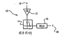
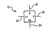
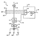
図1は、公知のルータセル10のブロック図である。このルータセル10は、入力(A)18、出力(Y)20、等化器12、スイッチ14およびリクロッカ回路16を含む。入力信号(A)18は典型的には、切り換えられる前の時点では等化器12に結合されており、これにより、信号の伝送媒体であるスタジオケーブルまたは他の媒体における損失が補償される。次いで、等化器12の出力は、スイッチ14の入力に結合される。スイッチ14は、入力信号(A)18と出力(Y)20との間を接続または切り離す。しかし、信号(Y)が出力される前に、当該信号はリクロッカ回路16によって処理される。リクロッカ回路16は、入力信号(A)18中のデータをリタイミングした後、その入力信号(A)18を、後続のルータセルへまたはスタジオ内の何らかのデバイスに対するルータマトリクスの外部へ伝送する。実際の信号切換システムにおいて、このリタイミング機能は、ルータを通じて切り換えられる信号内部のデータのタイミングの完全性を保障するために必要である。入力の最大数は1つの入力(A)18に限定されるため、図1に示すルータセル10は拡張不可能なものとして見なされる。
FIG. 1 is a block diagram of a
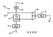
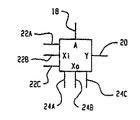
図2は、公知のルータセル10に1組の拡張入力ルータXi22および拡張出力ルータXo24を設けたブロック図である。図2に示すルータセル10は、図1に示すセルと同じ構成要素のほとんどを含む。しかし、図2において、拡張入力/出力組(Xi、Xo)22、24と、2対1の(2:1)マルチプレクサ26と、第2のリクロッカ回路16とが、ルータセルに追加されている。これらの構成要素を追加することで、図4を参照して以下にさらに示すように、ルータセル10を、ルータセルのマトリクスを形成することができるように拡張可能にすることが可能になる。
FIG. 2 is a block diagram in which a set of an extended input router Xi22 and an extended output router Xo24 are provided in a
このルータセル10において、拡張入力(Xi)22と、スイッチ14の出力とが、2:1マルチプレクサ26にルーティングされる。この2:1マルチプレクサ26は、入力(Xi)22または入力(A)18のうちいずれかを、第1のリクロッカ回路16からルータセル出力(Y)20へとルーティングされる対象として選択する。入力信号(A)18は、スイッチ14を通じてルーティングされ、次いで、第2のリクロッカ回路16に結合され、その後、拡張出力線(Xo)24に出力される。図3は、図2に示すルータセルを模式的に簡略化したものである。
In this
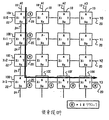
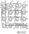
図4は、複数のルータセルを含む公知のルータマトリクスの概略図である。図2中に示すルータセル10を基本的な基礎的要素として用いると、1つのルータセルを他の1つ以上のセルと接続することにより、ルータマトリクスを作成することが可能である。例えば、図4に示すように、ルータセル10を16個用いて、入力が4つで出力が4つのルータマトリクスを構築することができる。これらのルータセル10を、複数の横列および縦列を含む2次元のマトリクス構造として構築する。信号入力A0、A1、A2およびA3(18)は、ルータマトリクスの上部に配置された第1の横列のルータセル10に結合される。拡張入力Xi0、Xi1、Xi2およびXi3(22)は、マトリクスの左端部に配置された第1の縦列のルータセル10に結合される。信号出力Y0、Y1、Y2およびY3(20)は、マトリクスの右端部に配置された最終縦列のルータセル10に結合される。そして、拡張出力Xo1、Xo2、Xo3およびXo4(24)は、ルータマトリクスの底部に配置された最終横列のルータセル10に結合される。次いで、マトリクス中の残りのセルは、図4に示すように構成され、これにより入力18、22が出力20、24に接続される。
FIG. 4 is a schematic diagram of a known router matrix including a plurality of router cells. When the
図4に示すルータにおいて、信号入力A0が出力Y3に接続されると、入力データ信号を7回リクロックする経路が生成される。A0にある信号は、A0からY3へと移動する際、ルータセル10A、10B、10C、10E、10Fおよび10G(すなわち、7個のルータセル)を通ってルーティングされる。このアーキテクチャから、このような様式で設計されたN×N個のルータを通過する最長経路を設けると、入力信号は2N−1回リクロックされることが分かる。従って、図4に示す4×4のマトリクスの場合、リクロックの回数は、2(4)−1すなわち7である。 In the router shown in FIG. 4, when the signal input A0 is connected to the output Y3, a path for reclocking the input data signal seven times is generated. As the signal at A0 travels from A0 to Y3, it is routed through router cells 10A, 10B, 10C, 10E, 10F, and 10G (ie, seven router cells). From this architecture, it can be seen that providing the longest path through N × N routers designed in such a manner, the input signal is reclocked 2N−1 times. Accordingly, in the case of the 4 × 4 matrix shown in FIG. 4, the number of reclocks is 2 (4) −1, that is, 7.
このルータ設計の欠点は、最長経路におけるリクロック回数が、ルータのサイズと共に直線的に拡張される点である。各リクロッカ回路からのジッタが蓄積すると、その結果、マトリクス中の各後続段においてデータをリタイミングすることがより困難になる。最終的には、データ信号中に蓄積されたジッタによって、リクロッカ回路16は、マトリクスを通じてルーティングされている信号をリタイミングできなくなり、その時点で、その信号は相対的に使用不可能となる。
A disadvantage of this router design is that the number of reclocks on the longest path scales linearly with the size of the router. The accumulation of jitter from each reclocker circuit results in more difficult retiming of data at each subsequent stage in the matrix. Eventually, the jitter accumulated in the data signal will prevent
本発明のルータマトリクスは、複数の入力ポートから複数の出力ポートに信号をルーティングするルータマトリクスであって、該ルータマトリクスは、該入力ポートと該出力ポートとの間に結合された、複数の相互接続されたルータセルであって、該相互接続されたルータセルは、2次元のマトリクスに構成された、ルータセルを備え、該ルータセルのそれぞれは、入力ポートと、出力ポートと、複数の拡張入力ポートと、複数の拡張入力ポートとを有し、該ルータセルは、該ルータマトリクスの最大パス長を低減するために、該入力ポート、該出力ポート、該複数の拡張入力ポートおよび該複数の拡張出力ポートを使用して相互接続されている。 The router matrix of the present invention is a router matrix for routing signals from a plurality of input ports to a plurality of output ports, the router matrix comprising a plurality of interconnected ports coupled between the input ports and the output ports. Connected router cells, wherein the interconnected router cells comprise router cells arranged in a two-dimensional matrix, each of the router cells having an input port, an output port, a plurality of extended input ports, A plurality of extended input ports, wherein the router cell uses the input port, the output port, the extended input ports, and the extended output ports to reduce a maximum path length of the router matrix. And are interconnected.
本発明のルータマトリクスは、前記少なくとも1つのルータセルは、少なくとも6個の他のルータセルに前記入力ポート、前記出力ポート、前記複数の拡張入力ポートおよび前記複数の拡張出力ポートを介して接続されてもよい。 In the router matrix of the present invention, the at least one router cell may be connected to at least six other router cells via the input port, the output port, the plurality of extended input ports, and the plurality of extended output ports. Good.
本発明のルータマトリクスは、前記相互接続されたルータセルを通じてルーティングされる信号が映像信号であってもよい。 In the router matrix of the present invention, a signal routed through the interconnected router cells may be a video signal.
本発明のルータマトリクスは、前記映像信号がHDTVデジタルビデオ信号であってもよい。 In the router matrix of the present invention, the video signal may be an HDTV digital video signal.
本発明のルータマトリクスは、ルータセルのそれぞれが、前記入力ポートと前記出力ポートとの間に結合されたスイッチであって、該スイッチは、入力信号を受け取る入力および第1のスイッチ出力と第2のパススルー出力との2個の出力を含む、スイッチと、該スイッチの該パススルー出力に結合された第1のリクロッカ回路と、複数の拡張出力信号を生成するために該第1のリクロッカ回路からの信号出力を複製する、該第1のリクロッカに結合されたファンアウト回路と、積分N:1マルチブレクサを有する第2のリクロッカ回路であって、Nは少なくとも3であり、該第2のリクロッカ回路は、前記複数の拡張入力ポートと、該スイッチからの該スイッチ出力とに結合され、出力信号を生成する、第2のリクロッカ回路とを含んでもよい。 The router matrix of the present invention is a switch wherein each of the router cells is coupled between the input port and the output port, the switch comprising an input for receiving an input signal and a first switch output and a second switch output. A switch including two outputs, a pass-through output, a first reclocker circuit coupled to the pass-through output of the switch, and a signal from the first reclocker circuit for generating a plurality of extended output signals. A fan-out circuit coupled to the first reclocker for duplicating an output, and a second reclocker circuit having an integral N: 1 multiplexer, wherein N is at least three, wherein the second reclocker circuit comprises: A second reclocker circuit coupled to the plurality of extended input ports and the switch output from the switch to generate an output signal. There.
本発明のルータマトリクスは、ルータセルのそれぞれは、前記入力ポートと前記スイッチの前記入力との間に結合された等化器をさらに含んでもよい。 The router matrix of the present invention may each further include an equalizer coupled between the input port and the input of the switch.
本発明のルータマトリクスは、Nは少なくとも4であってもよい。 In the router matrix of the present invention, N may be at least 4.
本発明のルータマトリクスは、ルータセルのそれぞれは、リクロッカ回路を含んでもよい。 In the router matrix of the present invention, each of the router cells may include a reclocker circuit.
本発明のルータマトリクスは、ルータセルのそれぞれは、前記複数の拡張入力ポートと前記入力ポートとに結合され、該複数の拡張入力ポートまたは該入力ポートの1つの上の信号を選択する拡張マルチプレクサと、該入力ポート上の信号を該複数の拡張出力ポートに複製するファンアウト回路とを含んでもよい。 A router matrix of the present invention, wherein each of the router cells is coupled to the plurality of extended input ports and the input port and selects an extended multiplexer for selecting the plurality of extended input ports or a signal on one of the input ports; A fan-out circuit for duplicating the signal on the input port to the plurality of extended output ports.
本発明のリクロッキング回路は、N個の入力信号を受け取り、該N個の入力信号から1つを選択するN:1マルチプレクサであって、Nは少なくとも3である、N:1マルチプレクサと、該N:1マルチプレクサの出力に結合されたリクロッカであって、該選択された入力信号中のデータをリタイミングするリクロッカとを備える。 The reclocking circuit of the present invention is an N: 1 multiplexer that receives N input signals and selects one from the N input signals, where N is at least three; A reclocker coupled to the output of the N: 1 multiplexer, the reclocker retiming data in the selected input signal.
本発明のリクロッキング回路は、Nは少なくとも4であってもよい。 In the reclocking circuit of the present invention, N may be at least 4.
本発明のリクロッキング回路は、Nは4よりも大きくてもよい。 In the reclocking circuit of the present invention, N may be greater than four.
本発明のリクロッキング回路は、前記入力信号が映像信号であってもよい。 In the reclocking circuit according to the present invention, the input signal may be a video signal.
本発明のリクロッキング回路は、前記映像信号がHDTVデジタルビデオ信号であってもよい。 In the reclocking circuit according to the present invention, the video signal may be an HDTV digital video signal.
本発明のルータセルは、ルータマトリクスに使用されるルータセルであって、該ルータセルの入力ポートと出力ポートとの間に結合されたスイッチであって、該スイッチは、入力信号を受け取る入力および第1のスイッチ出力と第2のパススルー出力との2個の出力を含む、スイッチと、該スイッチの該パススルー出力に結合された第1のリクロッカ回路と、複数の拡張出力信号を生成するために該第1のリクロッカ回路からの信号出力を複製する、該第1のリクロッカに結合されたファンアウト回路と、積分N:1マルチブレクサを有する第2のリクロッカ回路であって、Nは少なくとも3であり、該第2のリクロッカ回路は、該ルータセルの複数の拡張入力ポートと、該スイッチからの該スイッチ出力とに結合され、出力信号を生成する、第2のリクロッカ回路とを備える。 The router cell of the present invention is a router cell used in a router matrix, wherein the switch is a switch coupled between an input port and an output port of the router cell, the switch comprising an input receiving an input signal and a first switch. A switch including two outputs: a switch output and a second pass-through output; a first reclocker circuit coupled to the pass-through output of the switch; and a first reclocker circuit for generating a plurality of extended output signals. A fan-out circuit coupled to the first re-clocker for duplicating a signal output from the re-clocker circuit of the first re-clocker circuit, and a second re-clocker circuit having an integrating N: 1 multi-brixer, wherein N is at least 3; A second reclocker circuit is coupled to the plurality of extended input ports of the router cell and the switch output from the switch to generate an output signal. And a second reclocker circuit.
本発明のルータセルは、前記入力ポートと前記スイッチの前記入力との間に結合された等化器をさらに含んでもよい。 The router cell of the present invention may further include an equalizer coupled between the input port and the input of the switch.
本発明のルータセルは、Nは少なくとも4であってもよい。 In the router cell of the present invention, N may be at least 4.
複数の相互接続されたルータセルを備えるルータマトリクスを構成する場合に特に有用な改良されたリクロッカ回路およびルータセルが提供される。改良されたリクロッカ回路は、一体型N対1マルチプレクサ(MUX)を含む。ここで、Nは、少なくとも3である。改良されたルータセルは、リクロッカ/MUX回路、スイッチ、およびファンアウト回路を含む。複数のポートが、入力ポート、出力ポート、複数の拡張入力ポート、および複数の拡張出力ポートを含むルータセル回路に結合されている。改良されたルータセルは、入力ポートまたは拡張入力ポートのうちの1つのいずれかを、その出力ポートに結合し、また、入力ポートを、拡張出力ポートのそれぞれに結合する。ルータマトリクスの設計において、改良されたルータセルを用いることによって、リクロッカ回路によって引き起こされるジッターが最小限に抑えられる。 Improved reclocker circuits and router cells are provided which are particularly useful in constructing a router matrix with a plurality of interconnected router cells. The improved reclocker circuit includes an integrated N-to-1 multiplexer (MUX). Here, N is at least 3. The improved router cell includes a reclocker / MUX circuit, switch, and fan-out circuit. A plurality of ports are coupled to a router cell circuit including an input port, an output port, a plurality of extended input ports, and a plurality of extended output ports. The improved router cell couples either the input port or one of the extended input ports to its output port, and couples the input port to each of the extended output ports. By using the improved router cells in the design of the router matrix, the jitter caused by the reclocker circuit is minimized.
本発明の1つの局面によると、ルータマトリクスは、複数の入力ポートから、複数の出力ポートに信号をルーティングするために提供される。ルータマトリクスは、入力ポートと出力ポートとの間に結合されている、複数の相互接続されたルータセルを含む。ここで、相互接続されたルータセルは、2次元のマトリクスに構成される。ルータセルのそれぞれは、入力ポート、出力ポート、複数の拡張入力ポート、および複数の拡張出力ポートを含む。ルータセルは、ルータマトリクスを通じる最大パス長を低減し、ルーティングされる信号のリクロックの回数を低減するため、入力ポート、出力ポート、複数の拡張入力ポート、および複数の拡張出力ポートを用いて相互接続されている。 According to one aspect of the invention, a router matrix is provided for routing signals from a plurality of input ports to a plurality of output ports. The router matrix includes a plurality of interconnected router cells coupled between an input port and an output port. Here, the interconnected router cells are arranged in a two-dimensional matrix. Each of the router cells includes an input port, an output port, a plurality of extended input ports, and a plurality of extended output ports. Router cells are interconnected using input ports, output ports, multiple extended input ports, and multiple extended output ports to reduce the maximum path length through the router matrix and reduce the number of reclocks for routed signals. Have been.
本発明の他の局面によると、N個の入力信号を受信し、N個の入力信号のうちの1つを選択するN:1マルチプレクサを含む、改良されたリクロック回路が提供される。ここで、Nは、少なくとも3であり、リクロッカは、選択された入力信号のデータをリタイミングするために、N:1マルチプレクサの出力に結合されている。 According to another aspect of the present invention, an improved reclocking circuit is provided that includes an N: 1 multiplexer that receives N input signals and selects one of the N input signals. Here, N is at least 3 and the reclocker is coupled to the output of the N: 1 multiplexer to retime the data of the selected input signal.
本発明のさらに他の局面によると、ルータマトリクスにおいて用いられるルータセルが提供される。ルータセルは、(i)ルータセルの入力ポートと出力ポートとの間に結合されているスイッチであって、入力信号を受信する入力と、2つの出力、すなわち、第1のスイッチされる出力と、第2のパススルー出力とを含む、スイッチと、(ii)スイッチのパススルー出力に結合される第1のリクロッカ回路と、(iii)複数の拡張出力信号を生成するために第1のリクロッカ回路からの信号出力を複製する、第1のリクロッカに結合されているファンアウト回路と、(iv)一体型N:1マルチプレクサを有する第2のリクロッカ回路であって、Nは少なくとも3であり、第2のリクロッカ回路は、ルータセルの複数の拡張入力ポートと、スイッチからのスイッチされた出力とに結合され、出力信号を生成する、第2のリクロッカ回路とを含む。 According to yet another aspect of the present invention, there is provided a router cell for use in a router matrix. The router cell is (i) a switch coupled between an input port and an output port of the router cell, the input receiving an input signal, and two outputs, a first switched output, and a second output. (Ii) a first reclocker circuit coupled to the pass-through output of the switch, and (iii) a signal from the first reclocker circuit to generate a plurality of extended output signals. A fan-out circuit coupled to the first reclocker for duplicating the output, and (iv) a second reclocker circuit having an integrated N: 1 multiplexer, where N is at least 3 and wherein the second reclocker is The circuit includes a second reclocker circuit coupled to the plurality of extended input ports of the router cell and a switched output from the switch to generate an output signal. Including.
これらは、本発明の多くの局面のうちの一部に過ぎないことを、留意するべきである。特定されていない他の局面は、以下に説明する好適な実施形態の詳細な説明を読むことによって明らかになる。 It should be noted that these are only some of the many aspects of the present invention. Other aspects not specified will become apparent from a reading of the following detailed description of the preferred embodiments.
ルータマトリクスの設計において、改良されたルータセルを用いることによって、リクロッカ回路によって引き起こされる信号内のジッターが最小限に抑えられるようなリクロッカ回路およびルータセルを提供することができる。 By using an improved router cell in the design of the router matrix, a reclocker circuit and router cell can be provided in which the jitter in the signal caused by the reclocker circuit is minimized.
次に、残りの図面を参照すると、図5は、複数の拡張入力/出力対22A〜22C、24A〜24Cを有し、改良されたリクロッカ回路32を含む改良されたルータセル30のブロック図である。この改良されたルータセル30は、ルータマトリクスの形成において、同じタイプ、例えば、以下で図7および8について説明するようなタイプの他のルータセル30と組み合わせられて、特に有用である。このタイプのルータマトリクスは、例えば、テレビスタジオで映像信号を結合する映像ルータとして、特に有用である。これらの映像信号は、SDTVまたはHDTVテレビ信号のようなデジタル信号であってもよいし、他のタイプのデジタル映像信号であってもよい。しかし、本発明は、映像信号のルーティングに限定されるものではなく、スイッチング機構内で動作するリクロッキング(リタイミング)回路によって引き起こされるさらなるジッターを低減することが望ましい、任意のタイプのデジタル信号を、スイッチし、ルーティングするために用いられ得る。
Referring now to the remaining figures, FIG. 5 is a block diagram of an
図5に示す改良されたルータセル30は、入力信号ポート18(入力信号Aを受信する)、出力信号ポート20(信号Yを出力する)、複数の拡張入力ポート22A、22B、および22C(複数の拡張入力Xi0、Xi1、およびXi2を受信する)、ならびに、複数の拡張出力ポート24A、24B、および24C(複数の拡張出力Xo0、Xo1、およびXo2を受信する)を含み得る。ポート18、20、22、および24の間には、等化器12、スイッチ14、第1のタイプの第1のリクロッカ回路16、第2のタイプの第2のリクロッカ回路32、およびファンアウト回路36が結合されている。
The
第1のリクロッカ回路16は、公知のリクロッカ、例えば、Gennum GS9035と類似する。しかし、第2のリクロッカ32は、Gennum GS9035のような公知のリクロッカ部品16を含む改良されたリクロッカ回路である。また、第2のリクロッカ32は、N対1拡張マルチプレクサ34も含む。ここで、Nは、少なくとも3(すなわち、拡張マルチプレクサは、少なくとも3:1)である。第1のリクロッカ回路16および拡張マルチプレクサ34は、好適には、単一のデバイス、例えば集積回路に組み込まれるが、そうではなく、別個の部品であってもよい。
The
図5に示す改良されたルータセルは、以下で説明するように動作する。入力信号Aは、入力信号ポート18に結合され、等化器12にパススルーする。等化器12は、図1および2に示した等化器12と同様の様態で動作する。入力信号Aは、等化器12をパススルーし、その後、スイッチ14に結合される。スイッチ14は、1つの入力と、2つの出力14Aおよび14Bを有する。スイッチ14の1つの入力は、等化器12の出力と結合されている。第1の出力14Aは、スイッチされた出力であり、スイッチされた出力は、改良されたリクロッカ回路32のN:1MUX34の入力のうちの1つに結合されている。スイッチされた出力14Aは、スイッチ14の状態に依存して、入力信号Aに結合されるか、全く信号には結合されないかのいずれかである。入力信号Aは、スイッチへの入力に存在する。第2の出力14Bは、入力信号Aを単にパススルーさせるパススルー出力である。
The improved router cell shown in FIG. 5 operates as described below. Input signal A is coupled to input
第2の出力14Bのパススルー信号は、標準リクロッカ回路16に結合される。標準リクロッカ回路16は、入力信号Aについてリクロッカ(またはリタイミング)動作を行う。その後、リクロックされた信号は、リクロッカ16から、ファンアウト回路36へと出力される。ファンアウト回路36は、リクロッカ16から、複数の拡張出力ポート24A、24B、および24Cへとリクロックされた信号を結合し、複数の拡張出力信号Xo0、Xo1、およびXo2を提供する。
The pass-through signal at the second output 14B is coupled to a
スイッチされた出力14Aに加えて、改良されたリクロッカ回路32も、複数の拡張入力ポート22A、22B、および22Cに結合され、複数の拡張入力信号Xi0、Xi1、およびXi2を受信する。これらのライン(ポート)14A、22A、22B、22Cの信号は、N:1拡張マルチプレクサ34の入力に結合される。N:1拡張マルチプレクサ34は、上述したように、少なくとも3つ、おそらくは3より多い入力を含む。拡張マルチプレクサ34は、入力のうちの1つを選択し、選択された信号をリクロッカ16にルーティングする。リクロッカ16は、スイッチ14の第2の出力14Bに接続されるリクロッカ16と同じリクロッカ動作を行う。改良されたリクロッカ回路32からのリクロックされた信号は、出力信号Yとして、出力ポート20に提供される。
In addition to the switched
図6は、図5に示される改良されたルータセル30の簡略化された概略図である。この概略図は、入力信号Aを受け取るための入力ポート18を有するブラックボックスとしての改良されたルータセル30、出力信号Yを提供するための出力ポート20、複数の拡張入力信号Xiを受け取るための複数の拡張入力ポート22A、22B、22C、および複数の拡張出力信号XOを供給するための複数の拡張出力ポート24A、24B、24Cを示す。図6に示される簡略化された該略図は、複数の相互接続されたルータセルを含むルータマトリクス(またはルータ)を示すために用いられ得る。
FIG. 6 is a simplified schematic diagram of the
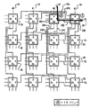
図7は、図5に示される複数の改良されたルータセルを含み、ルータマトリクスを介して第1のルーティング経路を明示する改良されたルータマトリクスの図である。図7に示されるルータマトリクスには4つの入力、図4に示されるルータマトリクスと同様に、16個のルータセルを含むルータマトリクス、4つの出力ルータマトリクスが存在する。しかし、図7のルータマトリクスでは、図5、6に示された改良されたルータセル30は、そのルータマトリクスを介してルーティングされた信号内のジッタを最小化する、より効率的なルータを生成するために用いられる。
FIG. 7 is a diagram of an improved router matrix that includes a plurality of the improved router cells shown in FIG. 5 and specifies a first routing path via the router matrix. The router matrix shown in FIG. 7 has four inputs, a router matrix including 16 router cells, and four output router matrices, similarly to the router matrix shown in FIG. However, in the router matrix of FIG. 7, the
図7に示されるルータマトリクスでは、各ルータセル30は、3つの拡張入力ポート22A、22B、22Cおよび3つの拡張出力ポート24A、24B、24Cを含み、従って、これらの拡張ポートおよび入出力ポート18、20を介して最大8つの他のルータセル30に接続され得る。この向上した接続性を用いることで、ルータマトリクスは、そのルータマトリクスを介する特定の経路に沿ってルータセルの数を最小化する様式(すなわち、リクロックキング動作)で構成され得る。
In the router matrix shown in FIG. 7, each
例えば、図4および図7に示される経路を検討する。図4では、入力A0から出力Y3までの経路は、7つのルータセル10A〜10Gを通過する。従って信号は7回リクロックされる。しかし、図7における同じ経路では、入力信号A0は、出力Y3に到達する前に3つのルータセル30A、30D、30Gのみを通過する。この低減した経路長は、ルータセル30Aの拡張出力ポート24A、24B、24Cを介してルータセル30Aをルータセル30B、30C、30Dに接続することによって、およびルータセル30Gの拡張入力ポート22A、22B、22Cを介してルータセル30Gをルータセル30D、30E、30Fに接続することによって、達成される。この様式でルータセル30Aを接続することによって、任意の入出力間のリクロックの最大数は、公知のルータ設計に対して実質的に低減される。
For example, consider the paths shown in FIGS. In FIG. 4, the path from the input A0 to the output Y3 passes through the seven router cells 10A to 10G. Thus, the signal is reclocked seven times. However, on the same path in FIG. 7, the input signal A0 passes only through the three
図7に示されるルータマトリクスは、4つの入力設計、4つの出力設計の簡単な例である。この簡単な例では、データ信号がリタイムされる回数は、最大7(公知のルータ設計)から最大3に低減される。本発明の有効な利得は、Nよりも大きいマトリクスとなることがさらにより明白になる。例えば、40×40ルータ(すなわちN=40)において、図2に示される公知のルータセル10および図4に示される公知のマトリクスが用いられる場合、リクロックの最大数が79(すなわち2N−1)である。しかし、図5に示される改良されたルータセルが、マトリクスを形成するために用いられる場合、経路に沿ったリブロックの最大数が7になる。図5に示される3つの拡張入力/出力の代わりに、2つの拡張入力/出力のみがセルごとに提供され、リブロックの最大数が7から11に増加する。いずれの場合にも、本発明の改良されたルータセルは、所与の経路に沿ったリクロッキング動作数の急激な減少を可能にする。
The router matrix shown in FIG. 7 is a simple example of four input designs and four output designs. In this simple example, the number of times the data signal is retimed is reduced from a maximum of seven (known router designs) to a maximum of three. It becomes even more apparent that the useful gain of the present invention results in a matrix larger than N. For example, if the known
図8は、ルータマトリクスを介する第2のルーティング経路を明示する、図7に示される改良されたルータマトリクスの概略図である。この経路において、入力信号A2は、ルータセル30Aおよび30Bを介して出力信号Y0にルーティングされる。従って、この経路を横断する場合、2つのリクロックが遭遇する。
FIG. 8 is a schematic diagram of the improved router matrix shown in FIG. 7, demonstrating a second routing path through the router matrix. In this path, input signal A2 is routed to output signal Y0 via
改良されたリクロッカ回路およびルータセルが提供される。このリクロッカ回路およびルータセルは、複数の相互接続されたルータセルを含むルータマトリクスに構成される場合に特に有用である。改良されたリクロッカ回路は、積分N対1マルチプレクサ(MUX)を含み、ここで、Nは少なくとも3である。改良されたルータセルは、リクロッカ/MUX回路と、スイッチと、ファンアウト回路とを含む。入力ポート、出力ポート、複数の拡張入力ポートおよび複数の拡張出力ポートを含む複数のポートがルータセル回路部に結合されている。改良されたルータセルは、その入力ポートまたは1つの拡張入力ポートのいずれかをその出力ポートに結合し、改良されたルータセルはまた、その入力ポートを拡張出力ポートのそれぞれに結合する。ルータマトリクスの設計にその改良されたルータセルを使用することにより、リクロッカ回路によって誘起されるジッタが最小化される。 An improved reclocker circuit and router cell are provided. The reclocker circuit and router cells are particularly useful when configured in a router matrix that includes a plurality of interconnected router cells. The improved reclocker circuit includes an integrating N-to-1 multiplexer (MUX), where N is at least three. The improved router cell includes a reclocker / MUX circuit, a switch, and a fan-out circuit. A plurality of ports including an input port, an output port, a plurality of extended input ports, and a plurality of extended output ports are coupled to the router cell circuit. The enhanced router cell couples either its input port or one extended input port to its output port, and the enhanced router cell also couples its input port to each of the extended output ports. By using the improved router cell in the design of the router matrix, the jitter induced by the reclocker circuit is minimized.
これらの図面を用いて本発明の例を説明してきたが、これは本発明の一例に過ぎず、上述のこの詳細な説明は、この例に本発明を限定することを意味しないことを理解すべきである。上述の本出願に対する、他の実施形態、改良、置換、代替、等価な要素および工程はまた、本発明の範囲内に存在する。 Although examples of the present invention have been described with reference to these drawings, it is understood that this is merely an example of the present invention, and that the detailed description above is not meant to limit the invention to this example. Should. Other embodiments, modifications, substitutions, alternatives, equivalent elements and steps to the above-mentioned application are also within the scope of the present invention.
ルータマトリクスの設計において、改良されたルータセルを用いることによって、リクロッカ回路によって引き起こされる信号内のジッターが最小限に抑えられるようなリクロッカ回路およびルータセルを提供することができる。 By using an improved router cell in the design of the router matrix, a reclocker circuit and router cell can be provided in which the jitter in the signal caused by the reclocker circuit is minimized.
32 リクロッカ回路 32 reclocker circuit
Claims (5)
該N:1マルチプレクサの出力に結合されたリクロッカであって、該選択された入力信号中のデータをリタイミングするリクロッカと
を備えた、リクロッキング回路。 An N: 1 multiplexer that receives N input signals and selects one from the N input signals, where N is at least 3;
A reclocker coupled to the output of the N: 1 multiplexer, the reclocker retiming data in the selected input signal.
Applications Claiming Priority (1)
| Application Number | Priority Date | Filing Date | Title |
|---|---|---|---|
| US09/690,771 US6791977B1 (en) | 2000-10-17 | 2000-10-17 | Reclocker circuit and router cell |
Related Parent Applications (1)
| Application Number | Title | Priority Date | Filing Date |
|---|---|---|---|
| JP2001319878A Division JP3585878B2 (en) | 2000-10-17 | 2001-10-17 | Improved reclocker and router cell |
Publications (1)
| Publication Number | Publication Date |
|---|---|
| JP2004166312A true JP2004166312A (en) | 2004-06-10 |
Family
ID=24773893
Family Applications (2)
| Application Number | Title | Priority Date | Filing Date |
|---|---|---|---|
| JP2001319878A Expired - Lifetime JP3585878B2 (en) | 2000-10-17 | 2001-10-17 | Improved reclocker and router cell |
| JP2004050546A Pending JP2004166312A (en) | 2000-10-17 | 2004-02-25 | Improved reclocker and router cell |
Family Applications Before (1)
| Application Number | Title | Priority Date | Filing Date |
|---|---|---|---|
| JP2001319878A Expired - Lifetime JP3585878B2 (en) | 2000-10-17 | 2001-10-17 | Improved reclocker and router cell |
Country Status (3)
| Country | Link |
|---|---|
| US (1) | US6791977B1 (en) |
| EP (1) | EP1199885A3 (en) |
| JP (2) | JP3585878B2 (en) |
Families Citing this family (4)
| Publication number | Priority date | Publication date | Assignee | Title |
|---|---|---|---|---|
| CN100454883C (en) | 2002-06-21 | 2009-01-21 | 汤姆森特许公司 | Fully redundant linear scalable broadcast router |
| DE10336992B4 (en) * | 2003-08-12 | 2006-02-02 | Hirschmann Electronics Gmbh & Co. Kg | Memory-free Retimer |
| US20090091345A1 (en) * | 2007-10-05 | 2009-04-09 | Moises Cases | Structure for providing a duplicate test signal of an output signal under test in an integrated circuit |
| CN114070286B (en) * | 2021-10-25 | 2023-05-26 | 中国电子科技集团公司第二十九研究所 | Arbitrary route radio frequency switch matrix |
Family Cites Families (23)
| Publication number | Priority date | Publication date | Assignee | Title |
|---|---|---|---|---|
| FR2462066B1 (en) * | 1979-07-17 | 1988-01-15 | Telecommunications Sa | DEVICE FOR SWITCHING TWO DIGITAL TRAINS |
| US4642805A (en) * | 1984-06-25 | 1987-02-10 | Rolm Corporation | Digital link for telephone station sets |
| ATE62774T1 (en) | 1985-09-25 | 1991-05-15 | Siemens Ag | NETWORK FOR PROCESSING DATA WITH A LARGE BIT WIDTH WITH ONE TRANSMITTER AND A NUMBER OF RECEIVERS. |
| GB2198012B (en) | 1986-11-20 | 1990-07-04 | Sony Corp | Clock signal multiplexers |
| DE8905982U1 (en) | 1989-05-12 | 1989-07-13 | Siemens AG, 1000 Berlin und 8000 München | Multi-stage coupling device |
| GB8927207D0 (en) | 1989-12-01 | 1990-01-31 | Pro Bel Limited | Digital switcher for routing signals |
| JPH0563734A (en) | 1991-08-28 | 1993-03-12 | Nec Corp | Data communication equipment |
| US5257260A (en) | 1991-12-18 | 1993-10-26 | Redcom Laboratories Inc. | Expanding switching capability of a time division communication system by multiplexing groups of circuits into successions |
| JPH0744544B2 (en) | 1992-01-17 | 1995-05-15 | 富士通株式会社 | Interconnection network with self-routing function |
| US5388099A (en) | 1992-10-22 | 1995-02-07 | Digital Equipment Corporation | Backplane wiring for hub in packet data communications system |
| US5751764A (en) | 1993-04-16 | 1998-05-12 | Nvision, Inc. | Switcher for flexibly interconnecting communication ports |
| GB9317897D0 (en) | 1993-08-27 | 1993-10-13 | Plessey Telecomm | Telecommunications switching element |
| US5577042A (en) * | 1994-01-18 | 1996-11-19 | Mcgraw Broadcast | Broadcast and presentation system and method |
| GB9408574D0 (en) | 1994-04-29 | 1994-06-22 | Newbridge Networks Corp | Atm switching system |
| JP3291122B2 (en) | 1994-06-02 | 2002-06-10 | 富士通株式会社 | Self-routing switch, ATM switch and switching system |
| US5689686A (en) | 1994-07-29 | 1997-11-18 | Cypress Semiconductor Corp. | Methods for maximizing routability in a programmable interconnect matrix having less than full connectability |
| US5493565A (en) * | 1994-08-10 | 1996-02-20 | Dsc Communications Corporation | Grooming device for streamlining a plurality of input signal lines into a grouped set of output signals |
| JP2914433B2 (en) | 1996-05-28 | 1999-06-28 | 日本電気株式会社 | Multi-stage switch connection information check method |
| US5734649A (en) | 1996-05-31 | 1998-03-31 | Bbn Corporation | Data packet router |
| US5798580A (en) | 1996-10-09 | 1998-08-25 | Morozov; Valentin | Contention free global interconnection |
| WO1998021857A1 (en) | 1996-11-14 | 1998-05-22 | Alan Huang | N-dimensional scalable switching networks |
| US6104732A (en) * | 1997-10-24 | 2000-08-15 | G-2 Networks, Inc. | Integrated signal routing circuit |
| FR2773296B1 (en) * | 1997-12-31 | 2000-01-21 | Alsthom Cge Alcatel | SUBSCRIBER CARD, SUBSCRIBER CONNECTION UNIT, AND SWITCHING CENTER FOR CONCENTRATING INTERNET FRAMES |
-
2000
- 2000-10-17 US US09/690,771 patent/US6791977B1/en not_active Expired - Lifetime
-
2001
- 2001-10-17 EP EP01124807A patent/EP1199885A3/en not_active Withdrawn
- 2001-10-17 JP JP2001319878A patent/JP3585878B2/en not_active Expired - Lifetime
-
2004
- 2004-02-25 JP JP2004050546A patent/JP2004166312A/en active Pending
Also Published As
| Publication number | Publication date |
|---|---|
| US6791977B1 (en) | 2004-09-14 |
| EP1199885A3 (en) | 2004-02-18 |
| JP2002171248A (en) | 2002-06-14 |
| EP1199885A2 (en) | 2002-04-24 |
| JP3585878B2 (en) | 2004-11-04 |
Similar Documents
| Publication | Publication Date | Title |
|---|---|---|
| KR920004917B1 (en) | Self-routing switching network | |
| JP5230707B2 (en) | Fully overlapping linearly extendable delivery router | |
| US6636932B1 (en) | Crossbar switch and control for data networks switching | |
| JP5150652B2 (en) | Synchronous network device | |
| CN1152984A (en) | Optical Telecom Network | |
| US6714537B1 (en) | Switch fabric architecture and techniques for implementing rapid hitless switchover | |
| CN1033915A (en) | Telecommunications digital switch | |
| US6754174B1 (en) | Interface for communications among network elements | |
| JP3585878B2 (en) | Improved reclocker and router cell | |
| US20020181482A1 (en) | Architectures for a single-stage grooming switch | |
| US20060209899A1 (en) | Switch for integrated telecommunication networks | |
| JP2000152356A (en) | Data changeover device | |
| JP2000152355A (en) | Switching module | |
| JP3034764B2 (en) | Optical communication device | |
| US7706417B1 (en) | Method of and circuit for generating a plurality of data streams | |
| KR100991413B1 (en) | Broadcast router configured to receive multiple or duplicate reference inputs alternately | |
| US11570125B2 (en) | Fast optical switch | |
| JP4944377B2 (en) | Linearly expandable distribution router device | |
| JP2003316749A (en) | Distributed link module | |
| JP2002009838A (en) | Method and apparatus for providing a client layer cross-connect function in a cross-connect or ADM | |
| US6888825B1 (en) | Cross-connect with shared storage | |
| US6826199B1 (en) | Arrangement, system and method relating to switching | |
| Salisbury et al. | Distributed, dynamic control of circuit-switched banyan networks | |
| JP2819922B2 (en) | Hi-Vision signal processing circuit test system | |
| KR0183135B1 (en) | Time switching device using synchronous ram and asynchronous ram |
Legal Events
| Date | Code | Title | Description |
|---|---|---|---|
| A621 | Written request for application examination |
Free format text: JAPANESE INTERMEDIATE CODE: A621 Effective date: 20040225 |
|
| A131 | Notification of reasons for refusal |
Free format text: JAPANESE INTERMEDIATE CODE: A131 Effective date: 20041014 |
|
| A601 | Written request for extension of time |
Free format text: JAPANESE INTERMEDIATE CODE: A601 Effective date: 20041227 |
|
| A602 | Written permission of extension of time |
Free format text: JAPANESE INTERMEDIATE CODE: A602 Effective date: 20050106 |
|
| A02 | Decision of refusal |
Free format text: JAPANESE INTERMEDIATE CODE: A02 Effective date: 20050610 |