JP2004152302A - Method and device for executing block cache in nonvolatile memory system - Google Patents
Method and device for executing block cache in nonvolatile memory system Download PDFInfo
- Publication number
- JP2004152302A JP2004152302A JP2003368148A JP2003368148A JP2004152302A JP 2004152302 A JP2004152302 A JP 2004152302A JP 2003368148 A JP2003368148 A JP 2003368148A JP 2003368148 A JP2003368148 A JP 2003368148A JP 2004152302 A JP2004152302 A JP 2004152302A
- Authority
- JP
- Japan
- Prior art keywords
- block
- logical
- physical
- physical block
- content
- Prior art date
- Legal status (The legal status is an assumption and is not a legal conclusion. Google has not performed a legal analysis and makes no representation as to the accuracy of the status listed.)
- Pending
Links
Images


Classifications
-
- G—PHYSICS
- G11—INFORMATION STORAGE
- G11C—STATIC STORES
- G11C16/00—Erasable programmable read-only memories
- G11C16/02—Erasable programmable read-only memories electrically programmable
-
- G—PHYSICS
- G06—COMPUTING; CALCULATING OR COUNTING
- G06F—ELECTRIC DIGITAL DATA PROCESSING
- G06F12/00—Accessing, addressing or allocating within memory systems or architectures
- G06F12/02—Addressing or allocation; Relocation
- G06F12/08—Addressing or allocation; Relocation in hierarchically structured memory systems, e.g. virtual memory systems
- G06F12/0802—Addressing of a memory level in which the access to the desired data or data block requires associative addressing means, e.g. caches
- G06F12/0866—Addressing of a memory level in which the access to the desired data or data block requires associative addressing means, e.g. caches for peripheral storage systems, e.g. disk cache
-
- G—PHYSICS
- G06—COMPUTING; CALCULATING OR COUNTING
- G06F—ELECTRIC DIGITAL DATA PROCESSING
- G06F12/00—Accessing, addressing or allocating within memory systems or architectures
- G06F12/02—Addressing or allocation; Relocation
- G06F12/0223—User address space allocation, e.g. contiguous or non contiguous base addressing
- G06F12/023—Free address space management
- G06F12/0238—Memory management in non-volatile memory, e.g. resistive RAM or ferroelectric memory
- G06F12/0246—Memory management in non-volatile memory, e.g. resistive RAM or ferroelectric memory in block erasable memory, e.g. flash memory
-
- G—PHYSICS
- G06—COMPUTING; CALCULATING OR COUNTING
- G06F—ELECTRIC DIGITAL DATA PROCESSING
- G06F12/00—Accessing, addressing or allocating within memory systems or architectures
- G06F12/02—Addressing or allocation; Relocation
- G06F12/08—Addressing or allocation; Relocation in hierarchically structured memory systems, e.g. virtual memory systems
- G06F12/0802—Addressing of a memory level in which the access to the desired data or data block requires associative addressing means, e.g. caches
-
- G—PHYSICS
- G06—COMPUTING; CALCULATING OR COUNTING
- G06F—ELECTRIC DIGITAL DATA PROCESSING
- G06F2212/00—Indexing scheme relating to accessing, addressing or allocation within memory systems or architectures
- G06F2212/20—Employing a main memory using a specific memory technology
- G06F2212/202—Non-volatile memory
- G06F2212/2022—Flash memory
-
- G—PHYSICS
- G06—COMPUTING; CALCULATING OR COUNTING
- G06F—ELECTRIC DIGITAL DATA PROCESSING
- G06F2212/00—Indexing scheme relating to accessing, addressing or allocation within memory systems or architectures
- G06F2212/72—Details relating to flash memory management
- G06F2212/7203—Temporary buffering, e.g. using volatile buffer or dedicated buffer blocks
Abstract
Description
本発明は、米国特許仮出願第60/421,910号(2002年10月28日出願)の優先権を主張し、この出願は、参考のため、本明細書中にその全体が援用される。 This invention claims priority to US Provisional Application No. 60 / 421,910, filed October 28, 2002, which is incorporated herein by reference in its entirety. .
(関連出願の相互参照)
本発明は、同時係属中の米国特許出願第10/281,739号、第10/281,823号、第10/281,670号、第10/281,824号、第10/281,631号、第10/281,855号、第10/281,762号、第10/281,696号、第10/281,626号および第10/281,804号、ならびに同時係属中の米国仮特許出願第60/421,725号、第60/421,965号、第60/422,166号、第60/421,746号および第60/421,911号(各々、2002年10月28日出願)に関し、これらの出願は、各々、参考のため、本明細書中にその全体が援用される。
(Cross-reference of related applications)
The present invention relates to co-pending U.S. patent applications Ser. Nos. 10 / 281,739, 10 / 281,823, 10 / 281,670, 10 / 281,824, and 10 / 281,631. Nos. 10 / 281,855, 10 / 281,762, 10 / 281,696, 10 / 281,626 and 10 / 281,804, and co-pending US provisional patent applications. Nos. 60 / 421,725, 60 / 421,965, 60 / 422,166, 60 / 421,746 and 60 / 421,911 (each filed on October 28, 2002) Each of these applications is hereby incorporated by reference herein in its entirety.
(発明の背景)
(1.発明の分野)
本発明は、概して、大容量デジタルデータ記憶システムに関する。より具体的には、本発明は、論理ブロックの論理ページと関連する更新されたコンテンツが、その論理ブロックに対応する物理ブロックに書き込まれる前にキャッシュされることを可能にするシステムおよび方法に関する。
(Background of the Invention)
(1. Field of the Invention)
The present invention relates generally to mass digital data storage systems. More specifically, the present invention relates to systems and methods that allow updated content associated with a logical page of a logical block to be cached before being written to a physical block corresponding to the logical block.
(2.関連技術の説明)
フラッシュメモリ記憶システム等の不揮発性メモリシステムは、このようなメモリシステムの物理サイズが小さく、繰返し再プログラムされるという不揮発性メモリの能力のために益々使用されている。フラッシュメモリ記憶システムの小さい物理サイズは、益々普及しつつあるデバイスにおけるこのような記憶システムの使用を容易にする。フラッシュメモリ記憶システムを用いるデバイスは、デジタルカメラ、デジタルカムコーダ、デジタルミュージックプレーヤー、ハンドヘルドパーソナルコンピュータおよびグローバルポジショニングデバイスを含むがこれらに限定されない。フラッシュメモリ記憶システムに含まれる不揮発性メモリに繰り返し再プログラムする能力は、フラッシュメモリ記憶システムが使用かつ再使用されることを可能にする。
(2. Description of Related Technology)
Non-volatile memory systems, such as flash memory storage systems, are increasingly being used due to the small physical size of such memory systems and the ability of non-volatile memory to be reprogrammed repeatedly. The small physical size of flash memory storage systems facilitates the use of such storage systems in increasingly popular devices. Devices that use flash memory storage systems include, but are not limited to, digital cameras, digital camcorders, digital music players, handheld personal computers, and global positioning devices. The ability to repeatedly reprogram non-volatile memory included in a flash memory storage system allows the flash memory storage system to be used and reused.
一般に、フラッシュメモリ記憶システムは、フラッシュメモリカードおよびフラッシュメモリチップセットを含み得る。フラッシュメモリチップセットは、通常、フラッシュメモリコンポーネントおよびコントローラコンポーネントを含む。通常、フラッシュメモリチップセットは、埋め込みシステムに組み入れられるように構成され得る。このようなアセンブリまたはホストシステムの製造業者は、通常、コンポーネントの形態のフラッシュメモリ、および他のコンポーネントを取得し、その後、フラッシュメモリおよび他のコンポーネントをホストシステムに組み入れる。 Generally, a flash memory storage system may include a flash memory card and a flash memory chipset. A flash memory chipset typically includes a flash memory component and a controller component. Typically, a flash memory chipset may be configured to be embedded in an embedded system. Manufacturers of such assemblies or host systems typically obtain flash memory and other components in the form of components, and then incorporate the flash memory and other components into the host system.
フラッシュメモリシステムの論理ブロックは、通常、物理ブロックにマッピングされる。例えば、32個の論理ページを含む論理ブロックは、32個の物理ページを含む物理ブロックにマッピングされ得る。論理ブロックと関連する、新しいか、または更新されたデータは、物理ブロックに書き込まれるべきであり、物理ブロックにデータを収容するための利用可能な空間がない場合、通常、予備物理ブロックが取得される。一旦予備物理ブロックが取得されると、新しいか、または更新されたデータは、もとの物理ブロックからのデータを有する予備物理ブロックにマージされる。 Logical blocks in a flash memory system are typically mapped to physical blocks. For example, a logical block that includes 32 logical pages may be mapped to a physical block that includes 32 physical pages. New or updated data associated with a logical block should be written to a physical block, and if there is no space available to accommodate the data in the physical block, a spare physical block is usually obtained. You. Once the spare physical block is obtained, the new or updated data is merged into the spare physical block with data from the original physical block.
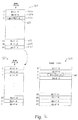
図1は、更新されたコンテンツを有する論理ブロック、および、更新されたコンテンツを収容するために取得され得る物理ブロックの概略図である。時間t1において、論理ブロック「A」202の第3の論理ページ204cに新しいデータが含まれるように、論理ブロック「A」202が更新される。第3の論理ページ204cと関連する物理ブロック「A]212の更新されたコンテンツが、物理ブロック「A」212に書き込まれ得ないほどまでに一杯である場合、物理ブロック「A」212は、新しい物理ブロック「B」222が取得され得る。物理ブロック「A」212の実質的にすべての物理ページ「A」212のコンテンツは、第3の物理ページ214cのコンテンツを除いて、第3の論理ページ204cと関連する更新されたコンテンツと共に物理ブロック「B」222に書き込まれ得る。その結果、物理ブロック「B」222は、時間t1において論理ブロック「A」202と関連する最新のデータを含む。一旦物理ブロック「B」222が書き込まれると、論理ブロック202は物理ブロック「B」222にマッピングされ、物理ブロック「A」212は、通常、消去される。更新されたコンテンツを物理ブロックに書き込む1つの従来のプロセスが図2を参照して後述される。
FIG. 1 is a schematic diagram of a logical block having updated content and a physical block that may be obtained to accommodate the updated content. At time t1, logical block "A" 202 is updated such that the third
時間t2において、物理ブロック「B」222にマッピングされる論理ブロック「A」202’が更新され、従って、第1の論理ページ204a’と関連するコンテンツは新しいか、または更新される。物理ブロック「B」222は、一杯になるか、または他の理由で、第1の論理ページ204a’に関連したコンテンツを含むように更新され得ないので、新しい物理ブロック「C」232が取得され得る。物理ブロック「B」222の実質的にすべての物理ページ224のコンテンツは、第1の物理ページ224aを除いて、第1の論理ページ214aと関連する更新されたコンテンツと共に物理ブロック「C」232に書き込まれ得、従って、物理ブロック「C」232は、時間t2において論理ブロック「A」202’と関連する最新データを含む。物理ブロック「B」222は、物理ブロック「C」232が論理ブロック「A」202’に書き込みおよびマッピングされた後に、通常、消去される。
At time t2, logical block "A" 202 ', which is mapped to physical block "B" 222, is updated, and thus the content associated with first
次に、図2を参照して、論理ブロックと関連するページの更新されたコンテンツを物理ブロックに書き込む1方法と関連する工程が記載される。論理ブロックと関連する更新されたページが物理ブロックに書き込まれることを可能にするプロセス250は、工程254にて開始し、ここで、例えば、論理ブロック「A」と関連するページ「X」等のページが更新される。論理ブロック「A」のページ「X」を更新する工程は、通常、ページ「X」と関連するコンテンツを変更する工程を包含する。一旦論理ブロック「A」のページ「X」が更新されると、論理ブロック「A」にマッピングされるか、そうでない場合、これと関連付けられるべき新しい物理ブロック「B」が、工程258において取得される。論理ブロック「A」と現在関連付けられている物理ブロックは、ページ「X」の更新されたコンテンツが書き込まれ得る利用可能な空間を有しない場合、新しい物理ブロック「B」が取得され得る。当業者によって理解されるように、新しい物理ブロック「B」が予備ブロックプールから取得され得る。
Referring now to FIG. 2, the steps associated with one method of writing updated content of a page associated with a logical block to a physical block will be described. The
工程262において、新しい物理ブロック「B」が取得された後、論理ブロック「A」と現在関連付けられている物理ブロック「A」の古いコンテンツは、論理ブロック「A」のページ「X」の更新されたコンテンツと共に物理ブロック「B」にマージされる。換言すると、物理ブロック「A」の実質的にすべてのコンテンツは、論理ブロック「A」のページ「X」と関連したコンテンツを除いて、論理ブロック「A」のページ「X」の更新されたコンテンツを有する論理ブロック「B」に書き込まれる。従って、物理ブロック「B」は、論理ブロック「A」と関連する最新のコンテンツを含む。
In
コンテンツが物理ブロック「B」に書き込まれた後、物理ブロック「A」は、工程266において消去され、工程270において、論理ブロック「A」との関連がはずされる。一旦物理ブロック「A」が消去され、かつ物理ブロック「A」との関連がはずされると、物理ブロック「A」は、通常、予備ブロックとして用いられるように利用可能であり、論理ブロックと関連する更新されたページが物理ブロックに書き込まれることを可能にするプロセスが完了する。
After the content has been written to physical block "B", physical block "A" is erased in
通常、物理ブロックにコンテンツを書き込むプロセス、および物理ブロックのコンテンツを消去するプロセスは時間がかかり、かつ、かなりの計算リソースを消費し得る。多くの場合、論理ブロックの論理ページが更新されるごとに1つの物理ブロックが書き込まれる一方で、もう一方の物理ブロックが消去される。従って、更新されるべきページが複数の場合、ブロックの消去が実質的に連続的に行われ得、新しいブロックが取得され得、かつ新しいブロックにデータが書き込まれ得る。ブロックを連続的に書き込む工程、およびブロックを消去する工程は、メモリシステムの性能を比較的著しく低下させ得る。 Typically, the process of writing content to physical blocks and erasing the content of physical blocks is time consuming and can consume significant computing resources. In many cases, one physical block is written each time a logical page of a logical block is updated, while the other physical block is erased. Thus, if there are multiple pages to be updated, the erasure of the block may occur substantially continuously, a new block may be obtained, and data may be written to the new block. The steps of writing blocks continuously and erasing blocks can relatively degrade the performance of the memory system.
従って、必要とされるのは、論理ページの更新に応答して生じる多数の書き込みおよび消去プロセスが低減されることを可能にする方法および装置である。特に、所望されるのは、物理ブロックドメインにおいて更新を実行する能力を実質的に損なうことなく、論理ブロックドメインにおける更新に対応する物理ブロックドメインにおける更新を実行することと関連する書き込みおよび消去の量が低減されることを可能にするシステムである。 Therefore, what is needed is a method and apparatus that allows a large number of write and erase processes that occur in response to logical page updates to be reduced. In particular, what is desired is the amount of writing and erasing associated with performing an update in the physical block domain that corresponds to an update in the logical block domain without substantially compromising the ability to perform the update in the physical block domain. Is a system that allows for a reduction in
(発明の要旨)
本発明による方法は、不揮発性メモリのブロックと関連するコンテンツを処理する方法であって、該不揮発性メモリは、メモリシステムと関連付けられ、該方法は、コンテンツの第1のセットを取得する工程であって、該コンテンツの第1のセットは、第1の論理ブロックの第1の論理グループと関連付けられ、該第1のグループは、該第1の論理ブロックと関連する第1の複数の論理ページを含み、該第1の論理ブロックは、第1の物理ブロックにマッピングされる、取得する工程と、該コンテンツの第1のセットをメモリ領域に書き込む工程と、該コンテンツの第1のセットを該メモリ領域から第2の物理ブロックの第1の物理グループに書き込む工程であって、該第1の物理グループは、該第2の物理ブロックと関連する第1の複数の物理ページを含む、書き込む工程と、該第2の物理ブロックを該第1の論理ブロックにマッピングする工程とを包含し、それにより上記目的が達成される。
(Summary of the Invention)
A method according to the invention is a method of processing content associated with a block of non-volatile memory, wherein the non-volatile memory is associated with a memory system, the method comprising the steps of obtaining a first set of content. Wherein the first set of content is associated with a first logical group of a first logical block, wherein the first group comprises a first plurality of logical pages associated with the first logical block. Wherein the first logical block is mapped to a first physical block, obtaining, writing the first set of content to a memory area, and storing the first set of content in the memory area. Writing from a memory area to a first physical group of a second physical block, wherein the first physical group comprises a first plurality of physical blocks associated with the second physical block. Including physical pages, it includes the step, and a step of mapping the second physical block to the logical block of the first writing, thereby the objective described above being achieved.
前記第1の物理ブロックは、コンテンツの第2のセットを含み、前記方法は、該コンテンツの第2のセットの少なくともいくつかを前記コンテンツの第1のセットを有する前記第2の物理ブロックに書き込む工程をさらに包含してもよい。 The first physical block includes a second set of content, and the method writes at least some of the second set of content to the second physical block having the first set of content. A step may be further included.
前記コンテンツの第2のセットを前記第1の物理ブロックから消去する工程と、該第1の物理ブロックと該第1の論理ブロックとのマッピングを実質的にはずす工程とをさらに包含してもよい。 The method may further include erasing the second set of content from the first physical block, and substantially removing a mapping between the first physical block and the first logical block. .
前記コンテンツの第1のセットを前記メモリ領域から消去する工程をさらに包含してもよい。 The method may further include erasing the first set of content from the memory area.
前記第1の物理ブロックは、コンテンツの第2のセットを含み、前記方法は、該コンテンツの第2のセットを前記メモリ領域に書き込む工程をさらに包含してもよい。 The first physical block may include a second set of content, and the method may further include writing the second set of content to the memory area.
前記コンテンツの第1のセットを前記メモリ領域に書き込む工程は、前記メモリ領域における前記コンテンツの第2のセットの少なくともいくつかを上書きする工程を包含してもよい。 Writing the first set of content to the memory area may include overwriting at least some of the second set of content in the memory area.
前記メモリ領域は、RAMキャッシュであってもよい。 The memory area may be a RAM cache.
前記コンテンツの第1のセットは、前記第1の論理ブロックと関連する更新を含んでもよい。 The first set of content may include updates associated with the first logical block.
コンテンツの第3のセットを取得する工程であって、前記コンテンツの第1のセットは、前記第1の論理ブロックの第2の論理グループと関連付けられ、該第2の論理グループは、該第1の論理ブロックと関連する第2の複数の論理ページを含む、取得する工程と、該コンテンツの第3のセットを前記メモリ領域に書き込む工程と、該コンテンツの第3のセットを該第2の物理ブロックの第2の物理グループに書き込む工程であって、該第2の物理グループは、該第2の物理ブロックと関連する第2の複数の物理ページを含む、工程とをさらに包含してもよい。 Obtaining a third set of content, wherein the first set of content is associated with a second logical group of the first logical block, wherein the second logical group is Obtaining, including a second plurality of logical pages associated with the first logical block, writing the third set of content to the memory area, and storing the third set of content in the second physical page. Writing to a second physical group of blocks, the second physical group including a second plurality of physical pages associated with the second physical block. .
前記第1の論理ブロックと関連する取得されるべきコンテンツのセットが実質的に他にない場合を判定する工程であって、取得されるべきコンテンツのセットが他にないと判定された場合、前記コンテンツの第1のセットおよび前記コンテンツの第3のセットが前記メモリ領域に書き込まれる、決定する工程をさらに包含してもよい。 Determining that there is substantially no other set of content to be obtained that is associated with the first logical block, and determining that there is no other set of content to be obtained, The method may further include determining that a first set of content and a third set of content are written to the memory area.
前記第1の論理ブロックと関連する取得されるべきコンテンツのセットが実質的に他にない場合を判定する工程は、第2の論理ブロックが更新されるべき場合を判定する工程を包含してもよい。 Determining when there is substantially no other set of content to be obtained that is associated with the first logical block may include determining when a second logical block is to be updated. Good.
前記第2の論理ブロックが更新されるべきであると判定された場合、前記方法は、該第2の物理ブロックを実質的に直ちに取得する工程と、前記コンテンツの第1のセットおよび前記コンテンツの第3のセットを該第2の物理ブロックに実質的に直ちに書き込む工程とをさらに包含してもよい。 If it is determined that the second logical block is to be updated, then the method includes obtaining the second physical block substantially immediately; Writing a third set to the second physical block substantially immediately.
前記第2の物理ブロックを取得する工程は、該第2の物理ブロックを前記第1の論理ブロックにマッピングする工程を包含してもよい。 Acquiring the second physical block may include mapping the second physical block to the first logical block.
コンテンツの前記第2のセットを前記第1の物理ブロックから消去する工程と、該第1の物理ブロックと前記第1の論理ブロックとのマッピングを実質的にはずす工程とをさらに包含してもよい。 The method may further include erasing the second set of content from the first physical block, and substantially removing a mapping between the first physical block and the first logical block. .
前記第2の物理ブロックを取得する工程と、該第2の物理ブロックを前記第1の論理ブロックにマッピングする工程とをさらに包含してもよい。 The method may further include a step of acquiring the second physical block and a step of mapping the second physical block to the first logical block.
前記第1の物理ブロックは、前記コンテンツの第1のセットを収容するように構成されてもよい。 The first physical block may be configured to contain a first set of the content.
前記メモリ領域は、第3の物理ブロックおよびRAMキャッシュの1つであってもよい。 The memory area may be one of a third physical block and a RAM cache.
前記不揮発性メモリは、NANDフラッシュメモリであってもよい。 The nonvolatile memory may be a NAND flash memory.
不揮発性メモリシステム内の第1の論理ブロックと関連する更新されたコンテンツを処理する方法であって、該第1の論理ブロックは、第1の物理ブロックにマッピングされ、該方法は、該第1の論理ブロックと関連する第1の更新を受信する工程であって、該第1の更新は、該第1の論理ブロックの第1の論理グループへの更新であり、該第1の論理グループは、該第1の論理ブロックと関連する第1の複数の論理ページを含むように構成される、受信する工程と、該第1の更新をキャッシュに記憶する工程と、該キャッシュのコンテンツを第2の物理ブロックに記憶する場合を判定する工程であって、該キャッシュのコンテンツは、該第1の更新を含む、判定する工程と、該キャッシュのコンテンツが該第2の物理ブロックに記憶されるべきであると判定された場合、該キャッシュのコンテンツを該第2の物理ブロックに記憶する工程であって、該キャッシュのコンテンツを記憶する工程は、該第1の更新を該第1の物理ブロックにおける第1の物理グループに記憶する工程を包含し、該第1の物理グループは、該第1の物理グループに含まれる第1の複数の物理ページを含む、記憶する工程と、該キャッシュのコンテンツが該第2の物理ブロックに記憶された後に、該第2の物理ブロックを該第1の論理ブロックにマッピングする工程と、該キャッシュのコンテンツが該第2の物理ブロックに記憶された後に、該第1の物理ブロックと該第1の論理ブロックとのマッピングをはずす工程とを包含し、それにより上記目的が達成される。 A method for processing updated content associated with a first logical block in a non-volatile memory system, wherein the first logical block is mapped to a first physical block, the method comprising: Receiving a first update associated with a first logical block of the first logical block, wherein the first update is an update to a first logical group of the first logical block, wherein the first logical group is Receiving, configured to include a first plurality of logical pages associated with the first logical block; storing the first update in a cache; Determining whether the content of the cache is stored in the second physical block, wherein the content of the cache includes the first update, and the content of the cache is stored in the second physical block. Storing the content of the cache in the second physical block, wherein storing the content of the cache comprises transmitting the first update to the first physical block. Storing in a first physical group, wherein the first physical group includes a first plurality of physical pages included in the first physical group; and storing the contents of the cache. Mapping the second physical block to the first logical block after is stored in the second physical block; and storing the contents of the cache in the second physical block after the is stored in the second physical block. Demapping the first physical block from the first logical block, thereby achieving the above object.
前記キャッシュのコンテンツを前記第2の物理ブロックに記憶する場合を判定する工程は、第2の論理ブロックが処理されるべき場合を判定する工程を包含し、該第2の論理ブロックが処理されるべきであると判定された場合、該キャッシュのコンテンツは、該第2の物理ブロックに記憶されてもよい。 Determining when to store the contents of the cache in the second physical block includes determining when a second logical block is to be processed, wherein the second logical block is processed. If so, the contents of the cache may be stored in the second physical block.
前記第2の物理ブロックを取得する工程をさらに包含してもよい。 The method may further include a step of acquiring the second physical block.
前記キャッシュのコンテンツは、前記第1の物理ブロックと関連する少なくともいくつかのコンテンツを含んでもよい。 The content of the cache may include at least some content associated with the first physical block.
前記第1の物理ブロックのコンテンツを前記キャッシュにコピーする工程であって、前記第1の更新は該キャッシュに記憶され、該第1の更新は、該第1の物理ブロックと関連する該コピーされたコンテンツの少なくとも一部分を実質的に上書きする、コピーする工程をさらに包含してもよい。 Copying the contents of the first physical block to the cache, wherein the first update is stored in the cache, and wherein the first update is the copy associated with the first physical block. May further include the step of substantially overwriting and copying at least a portion of the content.
前記キャッシュは、RAMキャッシュであってもよい。 The cache may be a RAM cache.
前記キャッシュのコンテンツを前記第2の物理ブロックに記憶する場合を判定する工程は、第2の論理ブロックが処理されるべき場合を判定する工程を包含し、該第2の論理ブロックが処理されるべきであると判定された場合、該キャッシュのコンテンツの少なくともいくつかが該第2の物理ブロックに記憶されてもよい。 Determining when to store the contents of the cache in the second physical block includes determining when a second logical block is to be processed, wherein the second logical block is processed. If so, at least some of the contents of the cache may be stored in the second physical block.
前記第2の論理ブロックが処理されるべきであると判定された場合、前記第1の物理ブロックの前記コンテンツの少なくともいくつかを前記第2の物理ブロックに記憶する工程をさらに包含してもよい。 If it is determined that the second logical block is to be processed, the method may further include storing at least some of the contents of the first physical block in the second physical block. .
前記キャッシュのコンテンツの少なくともいくつかが前記第2の物理ブロックに記憶された後で、前記第1の物理ブロックを消去する工程をさらに包含してもよい。 After at least some of the contents of the cache have been stored in the second physical block, the method may further include erasing the first physical block.
前記キャッシュは、物理ブロックキャッシュであってもよい。 The cache may be a physical block cache.
本発明は、更新、または論理ブロックと関連する新しいデータをキャッシュするシステムおよび方法に関する。本発明の1局面によると、不揮発性メモリのブロックと関連するコンテンツを処理する方法は、第1の論理ブロックと関連する第1のグループの論理ページと関連付けられるコンテンツの第1のセットを取得する工程と、およびコンテンツの第1のセットをメモリ領域に書き込む工程とを包含する。コンテンツの第1のセットは、その後、メモリ領域から第1の論理ブロックにマッピングされる第2の物理ブロックと関連する第1のグループの物理ページに書き込まれる。1実施形態において、メモリ領域は、RAMキャッシュおよび物理ブロックキャッシュの1つである。 The present invention relates to systems and methods for caching updates or new data associated with logical blocks. According to one aspect of the invention, a method of processing content associated with a block of non-volatile memory obtains a first set of content associated with a first group of logical pages associated with a first logical block. And writing the first set of content to the memory area. The first set of content is then written from a memory area to a first group of physical pages associated with a second physical block that is mapped to a first logical block. In one embodiment, the memory area is one of a RAM cache and a physical block cache.
別の実施形態において、第1の物理ブロックは、コンテンツの第2のセットを含み、この方法は、コンテンツの第2のセットの少なくともいくつかを、コンテンツの第1のセットと共に第2の物理ブロックに書き込む工程を包含する。このような実施形態において、コンテンツの第2のセットは、第1の物理ブロックから消去され得、第1の物理ブロックはマッピングされ得ないか、または、第1の論理ブロックとの関連が実質的にはずされ得る。 In another embodiment, the first physical block comprises a second set of content, and the method comprises: combining at least some of the second set of content with the first set of content in a second physical block. And writing the data to In such an embodiment, the second set of content may be erased from the first physical block, and the first physical block may not be mapped or substantially associated with the first logical block. Can be taken off.
論理ブロックと関連する、更新されたコンテンツであり得る新しいコンテンツをキャッシュすることは、論理ブロックと関連する、実質的にすべての新しいコンテンツが処理されるまで、新しいコンテンツが一時的に記憶されることを可能にする。処理されるべきすべての新しいコンテンツが処理された場合、論理ブロックにマッピングされるもとの物理ブロックの任意の適切なコンテンツと共に、新しいコンテンツの少なくともいくつかがコピーされ得、従って、論理ブロックと関連する最新のコンテンツが、新しい物理ブロックに書き込まれる。キャッシングプロセスを用いることによって、更新を処理することと関連する書き込み動作および読み出し動作の数、または論理ブロックと関連する新規の追加が、通常、低減され得る。従って、キャッシュプロセスを用いるメモリシステム全体の性能が強化され得る。 Caching new content, which may be updated content, associated with a logical block means that new content is temporarily stored until substantially all new content associated with the logical block has been processed. Enable. If all new content to be processed has been processed, at least some of the new content may be copied, along with any appropriate content of the original physical block that is mapped to the logical block, and thus associated with the logical block. The newest content is written to a new physical block. By using a caching process, the number of write and read operations associated with processing updates, or new additions associated with logical blocks, can typically be reduced. Therefore, the performance of the entire memory system using the cache process can be enhanced.
本発明の別の局面によると、不揮発性メモリシステム内の第1の論理ブロックと関連する更新されたコンテンツを処理する方法は、第1の論理ブロックと関連する第1の更新を受信する工程、第1の更新をキャッシュに記憶する工程と、キャッシュのコンテンツを第2の物理ブロックに記憶する場合を判定する工程とを包含する。この方法は、キャッシュのコンテンツが第2の物理ブロックに記憶されるべきであると判定された場合、第1の更新を含むキャッシュのコンテンツを第2の物理ブロックに記憶する工程をさらに包含する。第2の物理ブロックは、その後、第1の論理ブロックにマッピングされ得、第1の物理ブロックは、キャッシュのコンテンツが第2の物理ブロックに記憶された後、第1の物理ブロックとのマッピングがはずされ得る。 According to another aspect of the present invention, a method of processing updated content associated with a first logical block in a non-volatile memory system comprises: receiving a first update associated with a first logical block; Storing the first update in the cache and determining when to store the contents of the cache in the second physical block. The method further includes, if it is determined that the contents of the cache are to be stored in the second physical block, storing the contents of the cache including the first update in the second physical block. The second physical block may then be mapped to the first logical block, and the first physical block may be mapped to the first physical block after the contents of the cache are stored in the second physical block. Can be removed.
1実施形態において、キャッシュのコンテンツを第2の物理ブロックに記憶する場合を判定する工程は、第2の論理ブロックが処理されるべきであると判定する工程を包含する。第2の論理ブロックがプロセスされるべきであると判定された場合、キャッシュのコンテンツは、第2の物理ブロックに記憶される。別の実施形態において、キャッシュのコンテンツは、第1の物理ブロックと関連する少なくともいくつかのコンテンツを含む。 In one embodiment, determining when to store the contents of the cache in the second physical block includes determining that the second logical block is to be processed. If it is determined that the second logical block is to be processed, the contents of the cache are stored in a second physical block. In another embodiment, the content of the cache includes at least some content associated with the first physical block.
本発明のこれら、および他の利点は、以下の詳細な説明を読み、かつ図面の種々の図を検討することによって明らかになる。 These and other advantages of the present invention will be apparent from a reading of the following detailed description and a review of the various figures of the drawings.
本発明は、添付の図面と関連付けられた以下の説明を参照することによって最良に理解され得る。 The present invention may best be understood by reference to the following description taken in conjunction with the accompanying drawings.
本発明により、論理ページの更新に応答して生じる多数の書き込みおよび消去プロセスが低減されることを可能にする方法および装置が提供される。特に、所望されるのは、物理ブロックドメインにおいて更新を実行する能力を実質的に損なうことなく、論理ブロックドメインにおける更新に対応する物理ブロックドメインにおける更新を実行することと関連する書き込みおよび消去の量が低減されることを可能にするシステムである。 The present invention provides a method and apparatus that enables a number of write and erase processes that occur in response to logical page updates to be reduced. In particular, what is desired is the amount of writing and erasing associated with performing an update in the physical block domain that corresponds to an update in the logical block domain without substantially compromising the ability to perform the update in the physical block domain. Is a system that allows for a reduction in
(実施形態の詳細な説明)
物理ブロックを書き込みおよび物理ブロックを消去するプロセスは、相対的に時間がかかり、かつ、かなりの計算上のオーバーヘッドを用い得る。従って、書き込みおよび消去が比較的頻繁に行われる場合、物理ブロックを含むシステムの性能全体が不利な影響を受け得る。論理ブロックの論理ページが更新されるごとに論理ブロックにマッピングされる第1の物理ブロックが実質的に一杯である場合、第1の物理ブロックの更新およびいくつかのコンテンツが新しい物理ブロックに書き込まれ得る一方で、第1の物理ブロックが消去される。論理ブロックに関して複数のページが更新される場合、物理ブロックの消去が実質的に連続的に行われ、新しい物理ブロックが取得され、かつ新しい物理ブロックにデータが書き込まれ得る。物理ブロックが有効に連続的に書き込まれるか、または消去される場合、ブロックを含むメモリシステムの性能が低下され得る。
(Detailed description of the embodiment)
The process of writing physical blocks and erasing physical blocks is relatively time consuming and can use significant computational overhead. Thus, if writing and erasing are performed relatively frequently, the overall performance of the system, including the physical blocks, may be adversely affected. If the first physical block mapped to the logical block is substantially full each time a logical page of the logical block is updated, the update of the first physical block and some content are written to the new physical block. Meanwhile, the first physical block is erased. If multiple pages are updated for a logical block, erasure of the physical block may occur substantially continuously, a new physical block may be obtained, and data may be written to the new physical block. If a physical block is effectively continuously written or erased, the performance of the memory system containing the block may be degraded.
単一の論理ブロックにおける論理ページが連続的に更新される状態において、論理ブロックに対応する物理ブロックを書き込みおよび消去のために相当量の時間およびオーバーヘッドが費やされ得る。特に、論理ブロックにおける単一の論理ページが繰り返し更新され、論理ページへの更新ごとに「物理ブロックドメイン」において更新を実行する工程は、「論理ブロックドメイン」が連続的に変化する場合、物理ブロックドメインにおける更新が繰返し上書きされ得るため、特にむだであり得る。論理ブロックへの実質的にすべての更新が完了するまで物理ブロックの更新をしばらくの間待つことは、書き込み動作および消去動作の数が低減されることを可能にする。従って、メモリシステムの性能は改善され得る。 In a situation where logical pages in a single logical block are continuously updated, a considerable amount of time and overhead may be spent writing and erasing the physical block corresponding to the logical block. In particular, the step of repeatedly updating a single logical page in a logical block and performing an update in the “physical block domain” for each update to the logical page is performed when the “logical block domain” changes continuously. This can be particularly wasteful, as updates in the domain can be repeatedly overwritten. Waiting for a while for the physical block to be updated until substantially all updates to the logical block are completed allows the number of write and erase operations to be reduced. Thus, the performance of the memory system can be improved.
論理ブロック、または論理ブロックと関連する新しいデータへの更新をキャッシュするキャッシュプロセスの使用は、論理ブロックへの実質的にすべての更新または論理ブロックへの新しいデータの追加が終了するまで、更新がしばらくの間一時的に記憶されることを可能にする。少なくとも他の論理ブロックの処理が終わるまで、または、キャッシュが一杯の場合、論理ブロックへの更新データまたは新しいデータの追加がもはやなされないことが一旦有効に知られると、少なくともいくつかのキャッシュされた更新データおよび新しいデータが、論理ブロックへマッピングされるもとの物理ブロックの任意の適切なコンテンツと共にコピーされ得、従って、論理ブロックと関連する最新のコンテンツが新しい物理ブロックに書き込まれる。新しい物理ブロックが書き込まれた場合、もとの物理ブロックは消去され得る。その結果、複数の更新データまたは新規の追加を処理することと関連する書き込み動作および読み出し動作の数が低減され得る。本明細書中、および、後で議論を容易にするために、更新は、通常、新しいコンテンツを含む。同様に、ブロックにおけるコンテンツを更新する工程は、通常、ブロックに新しいコンテンツを追加する工程を含む。 The use of a cache process to cache updates to a logical block, or new data associated with the logical block, requires that the update be performed for a period of time until substantially all updates to the logical block or addition of new data to the logical block are complete. For temporary storage. At least until at least some other logical block has been processed, or if the cache is full, once it is effectively known that no updated or new data will be added to the logical block, at least some cached The update data and the new data can be copied along with any suitable content of the physical block that is to be mapped to the logical block, so that the latest content associated with the logical block is written to the new physical block. When a new physical block is written, the original physical block can be erased. As a result, the number of write and read operations associated with processing multiple update data or new additions may be reduced. Updates typically include new content herein and for ease of discussion later. Similarly, updating content in a block typically includes adding new content to the block.
ランダムアクセスメモリ(RAM)等のメモリが利用可能であるようなシステムのソフトウェア要件である場合、キャッシュは、RAMキャッシュであり得る。RAMキャッシュの使用は、通常、書き込みプロセスが効率的に行われることを可能にする。しかしながら、1実施形態において、利用可能なRAMの容量が不十分である場合、キャッシュは、ブロックキャッシュであり得る。すなわち、キャッシュは、物理ブロックであり得る。 If the software requirements of the system are such that a memory such as a random access memory (RAM) is available, the cache may be a RAM cache. The use of a RAM cache typically allows the writing process to be performed efficiently. However, in one embodiment, if the amount of available RAM is insufficient, the cache may be a block cache. That is, the cache may be a physical block.
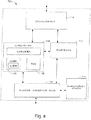
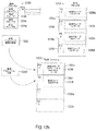
フラッシュメモリシステム、または、より一般的には、不揮発性メモリは、RAMキャッシュ、または更新データが物理ブロックに書き込まれる前に更新されたデータを一時的にキャッシュするブロックキャッシュの使用から利益を受け得る。通常、フラッシュメモリシステムは、ホストシステムとの関連で用いられ、従って、ホストシステムは、フラッシュメモリシステムにデータを書き込み得るか、ここからデータを読み出し得る。しかしながら、いくつかのフラッシュメモリシステムは、図3cを参照して後述されるように、埋め込みフラッシュメモリ、および、埋め込みフラッシュメモリのコントローラとして実質的に機能するようなホスト上で実行するソフトウェアを含む。図3aを参照して、例えば、コンパクトフラッシュ(R)メモリカード等の不揮発性メモリデバイスを含む一般的ホストシステムが記載される。ホストまたはコンピュータシステム100は、通常、マイクロプロセッサ108、ランダムアクセスメモリ(RAM)112、および入力/出力回路116が通信することを可能にするシステムバス104を含む。ホストシステム100が、通常、例えば、ディスプレイデバイスおよびネットワークデバイス等の他のコンポーネント(例示の目的で図示されない)を含み得る。
Flash memory systems, or more generally, non-volatile memory, may benefit from the use of RAM caches or block caches that temporarily cache updated data before the updated data is written to physical blocks. . Typically, a flash memory system is used in conjunction with a host system, so that the host system can write data to or read data from the flash memory system. However, some flash memory systems include embedded flash memory and software running on a host that substantially functions as a controller for the embedded flash memory, as described below with reference to FIG. 3c. Referring to FIG. 3a, a general host system including a non-volatile memory device such as, for example, a CompactFlash memory card is described. The host or computer system 100 typically includes a
一般的に、ホストシステム100は、静止画像情報、オーディオ情報、およびビデオ画像情報を含むが、これらに限定されない情報を取り込むことができ得る。このような情報は、リアルタイムで取り込まれ得、かつ無線方式でホストシステム100に転送され得る。ホストシステム100は、実質的に、任意のシステムであり得るが、ホストシステム100は、通常、デジタルカメラ、ビデオカメラ、セルラー通信デバイス、オーディオプレーヤまたはビデオプレーヤ等のシステムである。しかしながら、ホストシステム100は、通常、データまたは情報を記憶し、かつデータまたは情報を取り出す、実質的に、任意のシステムであり得る。 In general, host system 100 may be able to capture information including, but not limited to, still image information, audio information, and video image information. Such information can be captured in real time and transferred to the host system 100 wirelessly. The host system 100 can be virtually any system, but the host system 100 is typically a system such as a digital camera, a video camera, a cellular communication device, an audio player or a video player. However, host system 100 can typically be virtually any system that stores data or information and retrieves data or information.
ホストシステム100は、さらに、データを取り込むだけか、またはデータを取り出すかのどちらかのシステムであり得る。すなわち、ホストシステム100は、1実施形態において、データを記憶する専用システムであり得るか、またはホストシステム100は、データを読み出す専用システムであり得る。例示的に、ホストシステム100は、データを書き込むかまたは記憶するようにのみ構成されるメモリライタであり得る。あるいは、ホストシステム100は、ホストシステム100は、通常、データを読み込みまたは取り出し、データを取り込むことはしないように構成されたMP3プレーヤ等のデバイスであり得る。 Host system 100 may also be a system that either only captures data or retrieves data. That is, in one embodiment, host system 100 may be a dedicated system for storing data, or host system 100 may be a dedicated system for reading data. Illustratively, the host system 100 may be a memory writer configured to only write or store data. Alternatively, host system 100 may be a device, such as an MP3 player, that is typically configured to read or retrieve data but not capture data.
1実施形態において、除去可能な不揮発性メモリデバイスである不揮発性メモリデバイス120は、情報を記憶するためにバス104とインターフェース接続するように構成される。選択的インターフェースブロック130は、不揮発性メモリデバイス120がバス104と間接的にインターフェース接続することを可能にし得る。当業者によって理解されるように、入力/出力回路ブロック116は、存在する場合、バス104上に負荷がかかることを低減するために利用される。不揮発性メモリデバイス120は、不揮発性メモリ124および選択的メモリ制御システム128を含む。1実施形態において、不揮発性メモリデバイス120は、単一チップまたはダイ上にインプリメントされ得る。あるいは、不揮発性メモリデバイス120は、マルチチップモジュール上、または、チップセットを形成し得、かつ不揮発性メモリデバイス120として共に用いられ得る複数のディスクリートコンポーネント上にインプリメントされ得る。不揮発性メモリデバイス120の1実施形態において、図3bを参照してより詳細に後述される。
In one embodiment, the
例えば、NANDフラッシュメモリといったフラッシュメモリ等の不揮発性メモリ124は、データが必要に応じてアクセスおよび読み出しされ得るようにデータを記憶するように構成される。不揮発性メモリ124内に記憶されたデータは、さらに、適切に消去され得るが、不揮発性メモリ124内の特定のデータは、消去可能ではあり得ないことが理解されるべきである。データを記憶、データを読み出し、およびデータを消去するプロセスは、通常、メモリ制御システム128によって制御されるか、または、メモリ制御システム128が存在しない場合、マイクロプロセッサ108により実行されるソフトウェアによって制御される。不揮発性メモリ124の動作は、従って、基本的に、不揮発性メモリ124のセクションを実質的に等しく消耗させることによって、不揮発性メモリ124の寿命が実質的に最大化されるように管理され得る。
For example, a
不揮発性メモリデバイス120は、通常、選択的メモリ制御システム128、すなわちコントローラを含むことが記載された。多くの場合、不揮発性メモリデバイス120は、不揮発性メモリ124およびメモリ制御システム128、すなわちコントローラの機能の別個のチップを含み得る。例示的に、PCカード、コンパクトフラッシュ(R)カード、マルチメディアカード、およびセキュアデジタルカードを含むが、これらに限定されない不揮発性メモリデバイスは、別々のチップ上にインプリメントされ得るコントローラを含む一方で、他の不揮発性メモリデバイスは、別々のチップ上でインプリメントされるコントローラを含み得ない。当業者によって理解されるように、不揮発性メモリデバイス120が別々のメモリおよびコントローラチップを含まない実施形態において、メモリおよびコントローラ機能は、単一チップに統合され得る。あるいは、上述のように、例えば、不揮発性メモリデバイス120がメモリコントローラ128を含まない実施形態において、メモリ制御システム128の機能性は、マイクロプロセッサ108によって提供され得る。
図3bを参照して、不揮発性メモリデバイス120は、本発明の実施形態により、より詳細に説明される。上述のように、不揮発性メモリデバイス120は、不揮発性メモリ124を含み、かつ、メモリ制御システム128を含み得る。1実施形態において、メモリ124および制御システム128、またはコントローラは、不揮発性メモリデバイス120の一次コンポーネントであり得るが、メモリ124は、埋め込みNANDデバイスであり、例えば、不揮発性メモリデバイス120は、制御システム128を含み得ない。メモリ124は、半導体基板上に形成されるメモリセルのアレイであり得、ここで、データの1つ以上のビットは、2以上の電荷のレベルの1つをメモリセルの個々の記憶素子に記憶することによって個々のメモリセルに記憶される。電気的消去再書込み可能プログラム可能読み出し専用メモリ(EEPROM)は、このようなシステムの一般的なタイプのメモリの1例である。
Referring to FIG. 3b, the
制御システム128が不揮発性メモリデバイス120内に存在する場合、この制御システム128は、バス15を介してホストコンピュータ、またはデータを記憶するためにメモリシステムを用いる他のシステムに通信する。バス15は、通常、図3aのバス104の一部分である。制御システム128は、さらに、メモリ124の動作を制御し、これは、ホストにより提供されるデータを書き込み、ホストによってリクエストされるデータを読み出し、かつオペレーティングメモリ124における種々のハウスキーピング(house keeping)機能を実行するメモリセルアレイ11を含み得る。制御システム128は、通常、関連する不揮発性ソフトウェアメモリ、種々の論理回路等を有する多目的マイクロプロセッサを含む。多くの場合、1つ以上の状態マシンが、特定のルーチンの性能を制御するためにさらに含まれ得る。
If
メモリセルアレイ11は、1実施形態において、制御システム128、またはアドレス復号化器17を通じてマイクロプロセッサ108によってアドレス指定される。このような実施形態において、復号化器17は、制御システム128によってアドレス指定されるメモリセルのグループにデータをプログラムし、そこからデータを読み出すか、またはそれを消去するために、正確な電圧をアレイ11のゲートおよびビット線に印加する。さらなる回路19は、セルのアドレス指定されたグループにプログラムされるデータに依存する、アレイの素子に印加された電圧を制御するプログラミングドライバを含む。回路19は、センス増幅器、およびアドレス指定されたメモリセルのグループからデータを読み出すために必要とされる他の回路をさらに含む。アレイ11にプログラムされるべきデータ、またはアレイ11から最近読み出されたデータは、制御システム128と関連するバッファメモリ21に記憶され得るが、データは、その代わりに、他のバッファメモリ(図示せず)に記憶され得る。制御システム128は、通常、コマンドおよび状態データ等を一時的に記憶するための種々のレジスタもまた含み得る。
The
アレイ11は、多数のBLOCKS0−Nメモリセルに分割されることが多い。フラッシュEEPROMシステムについて一般的であるように、ブロックは、通常、消去の最小ユニットである。すなわち、各ブロックは、共に消去される最小数のメモリセルを含む。各ブロックは、通常、複数のページに分割される。当業者によって理解されるように、ページは、プログラミングの最小ユニットであり得る。すなわち、基本プログラミング動作は、最小限のメモリセルの1つのページにデータを書き込むか、またはここからデータを読み出し得る。1つ以上のデータのセクタは、各ページ内に記憶される。図3bに示されるように、1つのセクタは、ユーザデータおよびオーバーヘッドデータを含む。オーバーヘッドデータは、通常、セクタのユーザデータから計算されたエラー訂正コード(ECC)を含む。制御システム15の一部分23は、データがアレイ11にプログラムされる場合にECCを計算し、さらに、アレイ11からデータが読み出される場合、ECCをチェックする。あるいは、ECCは、異なったページ、またはこれらが属するユーザデータとは異なるブロックに記憶される。
ユーザデータの1セクタは、通常、512バイトであり、磁気ディスクドライブにおけるセクタのサイズに対応する。オーバーヘッドデータは、通常、さらなる16バイトであるが、オーバーヘッドデータは、通常、任意の数のバイトを含み得ることが理解されるべきである。データの1セクタは、最も一般的には、各ページに含まれるが、2つ以上のセクタは、その代わりにページを形成し得る。任意の数のページは、通常、ブロックを形成し得る。例示的に、ブロックは、8ページから512、1024またはそれ以上までのページから形成され得る。ブロックの数は、多くの場合、メモリシステムに所望のデータ記憶容量を提供するために選択される。アレイ11は、通常、いくつかのサブアレイ(図示せず)に分割され、これらの各々は、ブロックの一部分を含み、サブアレイは、種々のメモリ動作の実行において並列処理の程度を高めるために、互いにいくらか独立して動作する。複数のサブアレイの使用の例は、米国特許第5,890,192号に記載され、この出願は、参考のため、その全体が本明細書中に援用される。
One sector of user data is usually 512 bytes, corresponding to the size of a sector in a magnetic disk drive. It should be understood that overhead data is typically an additional 16 bytes, but overhead data can typically include any number of bytes. One sector of data is most commonly included on each page, but more than one sector may instead form a page. Any number of pages may typically form a block. Illustratively, a block may be formed from eight pages up to 512, 1024 or more pages. The number of blocks is often chosen to provide the memory system with the desired data storage capacity.
1実施形態において、不揮発性メモリは、例えば、ホストシステム等のシステムに埋め込まれる。図3cは、埋め込み不揮発性メモリを含むホストシステムの概略図である。ホストまたはコンピュータシステム150は、通常、マイクロプロセッサ158、RAM162、および入力/出力回路166が、ホストシステム150の他のコンポーネント(図示せず)の中で通信することを可能にするシステムバス154を含む。例えば、フラッシュメモリ等の不揮発性メモリ174は、情報がホストシステム150内に記憶されることを可能にする。インターフェース180は、不揮発性メモリ174とバス154との間に提供され得、情報が不揮発性メモリ174から読み出されおよびこれに書き込まれることを可能にする。
In one embodiment, the non-volatile memory is embedded in a system such as a host system, for example. FIG. 3c is a schematic diagram of a host system including embedded non-volatile memory. The host or
不揮発性メモリ174は、ソフトウェア、および不揮発性メモリ174を制御するように構成されるファームウェアのどちらか、または両方を有効に実行するマイクロプロセッサ158によって管理され得る。すなわち、マイクロプロセッサ158は、コードデバイス(図示せず)、すなわち、ソフトウェアコードデバイスまたはファームウェアコードデバイスを動作させ得、これは、不揮発性メモリ174が制御されることを可能にする。CPU内部マイクロプロセッサ158、別個のフラッシュROM、または内部不揮発性メモリ174で実装されるフラッシュメモリであり得るこのようなコードデバイス(後述される)は、不揮発性メモリ174における物理ブロックがアドレス指定されることを可能にし得、かつ、情報が物理ブロックに記憶され、ここから読み出され、かつここから消去されることを可能にし得る。
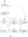
論理ブロックと関連する新しいか、または更新されたデータが受信された場合、例えば、論理ブロックと関連する更新が、実質的に完了し、かつ、異なった論理ブロックと関連する更新が処理されるべきときまで、データは、RAMキャッシュにて一時的にキャッシュされ得る。図4aは、論理ブロック、物理ブロック、および、本発明による実施形態による論理ブロックと関連する更新をキャッシュするように構成されるRAMキャッシュの概略図である。例えば、NANDフラッシュメモリメモリコンポーネント等の不揮発性メモリコンポーネントに配置される物理ブロック「A」410は、論理ブロック「A」400にマッピングされる。記載された実施形態において、物理ブロック「A」410は、実質的に一杯であり、従って、論理ブロック「A」400と関連する更新されたか、または新しいコンテンツを受取り得ない。従って、論理ブロック「A」400の論理ページ402cのコンテンツが更新された場合、更新されたコンテンツ406は、物理ブロック「A」410に記憶され得ない。その代わりに、更新されたコンテンツ406は、物理ブロック「A」410がRAMキャッシュ420にコピーまたはキャッシュされた後、RAMキャッシュ420に一時的に記憶されるか、そうでない場合、これに書き込まれ、すなわち、キャッシュされる。
If new or updated data associated with a logical block is received, e.g., the update associated with the logical block is substantially completed, and the update associated with a different logical block should be processed Until then, data may be temporarily cached in a RAM cache. FIG. 4a is a schematic diagram of a RAM cache configured to cache logical blocks, physical blocks, and updates associated with logical blocks according to embodiments according to the present invention. For example, a physical block "A" 410 located in a non-volatile memory component such as a NAND flash memory component is mapped to a logical block "A" 400. In the described embodiment, physical block “A” 410 is substantially full, and thus cannot receive updated or new content associated with logical block “A” 400. Therefore, when the content of the logical page 402c of the logical block “A” 400 is updated, the updated
更新されたコンテンツ406をRAMキャッシュ420に書き込む工程は、RAMキャッシュ420に含まれる古いコンテンツを上書きする工程を包含することが理解されるべきである。例えば、更新されたコンテンツ406は、RAMキャッシュ420に予め記憶された古いデータコンテンツを上書きし得る。RAMキャッシュ420がメモリシステム全体の中の実質的にどこにでも配置され得る一方で、1実施形態において、RAMキャッシュ420は、不揮発性メモリコンポーネント、従って、物理ブロック「A」410を有効に制御するコントローラと関連付けられ得る。
It should be understood that writing updated
実質的に、任意の他のブロック(図示せず)が更新されるべき前に、論理ブロック「A」400に次の更新がなされる場合、次の更新は、さらに、RAMキャッシュ420に記憶され得る。図4bに示されるように、論理ブロック「A」400のページ402eと関連するコンテンツ426が更新された場合、更新されたコンテンツ426は、RAM内の実質的に任意の適切な場所におけるRAMキャッシュ420にキャッシュされ得る。論理ブロック「A」400と関連する更新の現在のセットが完了するまで、更新は、実質的に連続的にRAMキャッシュ420に記憶され得る。論理ブロック「A」400への更新の現在のセットは、1実施形態において、論理ブロック「A」400への実質的にすべての更新であり得、これは、異なった論理ブロック(図示せず)と関連する更新が処理される前に処理され得る。
If the next update is made to logical block "A" 400 before substantially any other block (not shown) is to be updated, the next update is further stored in RAM cache 420. obtain. As shown in FIG. 4b, if the
論理ブロック「A」400への更新の現在のセットがすべてRAMキャッシュ420にキャッシュされた場合、例えば、更新されたコンテンツ406、426等の、RAMキャッシュ420に一時的に記憶された更新は、新しい物理ブロックに書き込まれるか、そうでない場合、これにコピーされ得る。図4cは、物理ブロックおよびRAMキャッシュ、すなわち、図4bの物理ブロック410およびRAMキャッシュ420の概略図であり、本発明の実施形態による新しい物理ブロックに書き込まれるべきコンテンツを伴う。
If the current set of updates to logical block "A" 400 have all been cached in RAM cache 420, then the updates temporarily stored in RAM cache 420, such as updated
一般に、論理ブロック「A」400と関連する最新または最近のコンテンツは、物理ブロック「B」440に書き込まれ得る。論理ブロック「A」400と関連する最新のコンテンツは、実質的にすべてRAMキャッシュ420内に含まれる。従って、RAMキャッシュ420のコンテンツを物理ブロック「B」440にコピーする工程は、物理ブロック「B」440が、本質的に物理ブロックドメイン内の論理ブロック「A」400のバージョンであることを可能にする。物理ブロック「B」440は、論理ブロック「A」400と関連する実質的にすべての現在の情報を含む場合、物理ブロック「A」410は消去され得、かつ、論理ブロック「A」400との関連がはずされるか、またはマッピングがはずされ得る。その結果、論理ブロック「A」400は、通常、任意の所与の時間にて単一の物理ブロックのみにマッピングされる。従って、システム内の物理ブロックの使用は、物理ブロック「B」440が論理ブロック「A」400と関連付けられ、物理ブロック「A」410と論理ブロック「A」400との関連がはずされ、かつ、予備ブロックプールに戻され得るのと実質的に同時に有効に節約される。 In general, the latest or recent content associated with logical block "A" 400 may be written to physical block "B" 440. The most recent content associated with logical block “A” 400 is contained substantially in RAM cache 420. Thus, copying the contents of RAM cache 420 to physical block "B" 440 allows physical block "B" 440 to be essentially a version of logical block "A" 400 in the physical block domain. I do. If physical block "B" 440 contains substantially all current information associated with logical block "A" 400, physical block "A" 410 can be erased and logical block "A" 400 The association may be disassociated or the mapping may be disassociated. As a result, logical block "A" 400 is typically mapped to only a single physical block at any given time. Thus, the use of physical blocks in the system is such that physical block "B" 440 is associated with logical block "A" 400, physical block "A" 410 is disassociated with logical block "A" 400, and Effective savings are made substantially at the same time as they can be returned to the spare block pool.
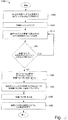
次に、図5を参照して、RAMキャッシュの使用を通じて物理ブロックドメインにおけるページのコンテンツを更新する1方法と関連する工程が、本発明の実施形態により記載される。RAMキャッシュを用いてページを一時的に記憶するプロセス500は、工程504にて開始し、ここで、ホストは、論理ブロック「A」の処理を開始する。例えば、不揮発性メモリは、インターフェース接続するシステム、または不揮発性メモリが埋め込まれるシステム等のホストは、論理ブロック「A」内に含まれるページと関連する更新を処理する場合、論理ブロック「A」の処理を開始し得る。
Referring now to FIG. 5, one method of updating the contents of a page in the physical block domain through the use of a RAM cache will be described in accordance with an embodiment of the present invention. The
論理ブロック「A」と関連する物理ブロック「A」において利用可能な空間が実質的にない場合、物理ブロック「A」は、更新を有効に収容することができない。従って、RAMキャッシュは、更新が新しい物理ブロックに記憶される前に更新をキャッシュするために用いられ得る。工程504から、プロセスフローは、工程505に進み、ここで、新しい物理ブロック「B」が取得される。新しい物理ブロック「B」が、例えば、予備ブロックのセット等から取得されて、マッピングされるか、そうでない場合、論理ブロック「A」と関連付けられる。物理ブロック「A」の実質的にすべてのコンテンツは、工程506においてRAMキャッシュにキャッシュまたは書き込まれ得る。工程508において、論理ブロック「A」に含まれるページへの更新は、例えば、コントローラ等によってRAMキャッシュに記憶される。通常、更新は、更新されたデータまたは新しいデータを含み得、更新は、物理ブロック「A」と関連するデータがRAMキャッシュにて上書きされるようにし得る。上述のように、図4a〜図4cを参照して、RAMキャッシュは、RAM、または更新データを一時的に記憶する際に用いるために利用可能である同様のメモリである。一旦論理ページへの更新がRAMキャッシュに記憶されると、工程512において、例えば、論理ブロック「B」等の異なった論理ブロックの処理を開始する準備ができているか否かに関する判定が下される。換言すると、別のブロックが処理される前に、RAMキャッシュに記憶されることを必要とする論理ブロック「A」と関連する任意のさらなる更新がなされるか否かが判定される。
If there is substantially no space available in the physical block “A” associated with the logical block “A”, the physical block “A” cannot effectively accommodate updates. Thus, the RAM cache can be used to cache updates before they are stored in a new physical block. From
工程512において、論理ブロック「B」の処理を開始するときではないと判定された場合、論理ブロック「A」と関連するさらなる更新があることを示す。従って、プロセスフローは、工程508に戻り、ここで、論理ブロック「A」と関連する更新がRAMキャッシュに記憶される。あるいは、本質的に、異なった論理ブロックを処理するときではないと判定された場合、RAMキャッシュのコンテンツは、工程518において、物理ブロック「B」に書き込まれ、従って、論理ブロック「A」と関連する最新のコンテンツが物理ブロック「B」にて記憶または書き込まれる。
If
一旦情報が物理ブロック「B」に記憶されると、物理ブロック「A」は、工程524において消去される。RAMキャッシュに記憶される情報は上書きされ得るので、RAMキャッシュのコンテンツが物理ブロック「B」にマージされた後で、RAMキャッシュを消去することは、通常、必要とされないことが理解されるべきである。通常、別の物理ブロックのコンテンツが、RAMキャッシュに記憶された場合、RAMキャッシュの前のコンテンツが上書きされる。しかしながら、1実施形態において、一旦RAMキャッシュのコンテンツが物理ブロック「B」にマージされると、RAMキャッシュは消去され得る。
Once the information is stored in physical block "B", physical block "A" is erased in
工程524において、物理ブロック「A」が消去された後、工程528において、物理ブロック「A」と論理ブロックとの関連がはずされる。物理ブロック「A」と論理ブロック「A」との関連をはずす工程は、マッピングを更新して、論理ブロック「A」が物理ブロック「B」と関連付けられることを示す工程を包含し得る。物理ブロック「A」と論理ブロック「A」との関連をはずす工程の後で、論理ブロックと関連するページ更新を一時的に記憶するためにRAMキャッシュを用いるプロセスが完了する。
After the physical block “A” is erased in
更新を物理ブロックに書き込む前に、論理ブロックと関連する更新を一時的に記憶するためにRAMキャッシュを用いることは有効であるが、メモリシステムは、RAMキャッシュとして用いるために利用可能なRAMを常に有しているわけではあり得ない。通常、RAMキャッシュは、ブロックの実質的にすべてのコンテンツを収容し得るサイズである。従って、RAMキャッシュのサイズは、システム内の物理ブロックのサイズに依存して異なり得る。例えば、システム内の物理ブロックが、通常、約32ページを含む場合、RAMキャッシュは、少なくとも約32ページのブロックのコンテンツを収容するために十分な大きさのサイズであり得る。ソフトウェアの必要があり、物理ブロックを収容するために適切なサイズのRAMキャッシュが利用可能でないというような場合、実際の物理ブロックは、その代わりに、情報が論理ブロックと関連する物理ブロックに書き込まれる前に、情報を一時的に保持するために用いられ得る。換言すると、RAMキャッシュである「キャッシュブロック」をインプリメントするのではなく、その代わりに物理ブロックがインプリメントされ得るキャッシュブロックをインプリメントする。 Although it is useful to use a RAM cache to temporarily store updates associated with logical blocks before writing updates to physical blocks, memory systems always use available RAM to use as a RAM cache. You cannot have it. Typically, a RAM cache is sized to accommodate substantially all of the contents of a block. Therefore, the size of the RAM cache can vary depending on the size of the physical blocks in the system. For example, if a physical block in a system typically contains about 32 pages, the RAM cache may be large enough to accommodate at least about 32 pages of block content. If there is a need for software, such as when an appropriately sized RAM cache is not available to accommodate the physical block, the actual physical block is instead written to the physical block whose information is associated with the logical block Previously, it could be used to temporarily hold information. In other words, rather than implementing a "cache block" which is a RAM cache, instead implement a cache block in which a physical block may be implemented.
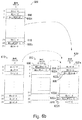
図6aは、論理ブロック、物理ブロック、および、本発明の実施形態による論理ブロックと関連する更新をキャッシュするように構成される、例えば、物理ブロックキャッシュ等のキャッシュブロックの概略図である。不揮発性メモリコンポーネントの物理ブロック「A」610が論理ブロック「A」600にマッピングされる。物理ブロック「A」610が実質的に一杯であり、実際に、論理ブロック「A」600と関連して更新されたか、または新しいコンテンツを収容することができない場合、物理ブロックキャッシュ612は、更新されるか、または新しいコンテンツを一時的にキャッシュするために用いられ得る。
FIG. 6a is a schematic diagram of a logical block, a physical block, and a cache block, such as a physical block cache, configured to cache updates associated with the logical block according to an embodiment of the present invention. Physical block “A” 610 of the non-volatile memory component is mapped to logical block “A” 600. If the physical block “A” 610 is substantially full and, in fact, has been updated in relation to the logical block “A” 600 or cannot accommodate new content, the
示されるように、論理ブロック60の論理ページ602cは、更新されたコンテンツ606を含む。更新されたコンテンツ606が論理ページ602cと関連付けられるという表示が物理ブロックキャッシュ612に記憶されるか、または利用可能であり、従って更新されたコンテンツ606が論理ページ602cと関連付けられるとして識別され得る場合、更新されたコンテンツ606は、物理ブロックキャッシュ612内の、実質的にどこにでも記憶され得る。例示的に、更新されたコンテンツ606は、示されるように、物理ブロックキャッシュ612内の第1の利用可能なページにキャッシュされ得る。あるいは、1実施形態において、更新されたコンテンツ606は、論理ページ602cと対応する場所における物理ブロックキャッシュ612に書き込まれるか、またはキャッシュされ得る。
As shown,
例えば、更新されたコンテンツ616が論理ページ602eと関連付けられる場合等、有効になされた次の更新がある場合、更新されたコンテンツ616は、さらに、物理ブロックキャッシュ612にキャッシュされ得る。例えば、異なった論理ブロック(図示せず)を処理するときである場合等、一旦論理ブロック「A」600と関連する実質的にすべての更新が、少なくとも一時的に完了すると、図6bを参照して説明されるように、更新606、616を含む、論理ブロック「A」600と関連する最新データが新しい物理ブロックに書き込まれ得る。いくつかの実施形態において、論理ブロック「A」600と関連する「最新データ」は、更新のみを含み得る一方で、示されるような実施形態を含む他の実施形態において、論理ブロック「A」600と関連する最新データは、更新606、616、および、更新606、616によって奪われなかった物理ブロック「A」610のいくつかのコンテンツを含み得る。異なった論理ブロック(図示せず)を処理するときではない場合でさえ、物理ブロックキャッシュ612が一杯である場合、論理ブロック「A」600と関連する最新コンテンツを新しい物理ブロックに供給するために、マージ動作または同様の動作が行われることが理解されるべきである。新しい物理ブロックは、その後、「古い」物理ブロックになり得、論理ブロック「A」600と関連するさらなる更新が、新しい物理ブロックキャッシュ612にキャッシュされ得る。
The updated
図6bに示されるように、異なった論理ブロックが処理されるべきであると仮定すると、論理ブロック「A」600にマッピングされる新しい物理ブロック「B」620が取得され得る。新しい物理ブロック「B」620が必要に応じて取得され得るか、または、1実施形態において、論理ブロック「A」600と関連するキャッシュプロセスが最初に開始する場合に取得され得ることが理解されるべきである。一般に、論理ブロック「A」600と関連する最新または最近のコンテンツは、物理ブロック「B」620に書き込まれ得る。多くの場合、論理ブロック「A」600と関連する最新のコンテンツは、物理ブロック「A」610および物理ブロックキャッシュ612の両方に含まれ得る。特に、論理ブロック「A」600の実質的に任意の更新されたコンテンツは、物理ブロックキャッシュ612に含まれる一方で、古いコンテンツ、または更新の現在のセットの結果として更新されなかったコンテンツが物理ブロック「A」610に含まれる。例えば、より新規に更新されたコンテンツ(図示せず)が更新されたコンテンツ606を有効に奪い得る等、論理ブロック「A」600のいくつかの更新されたコンテンツは、論理ブロック「A」600内にも含まれる、より最近更新されたコンテンツによって奪われ得ることが理解されるべきである。
As shown in FIG. 6b, assuming that a different logical block is to be processed, a new physical block “B” 620 that maps to logical block “A” 600 may be obtained. It is understood that a new physical block “B” 620 may be obtained as needed or, in one embodiment, may be obtained when a cache process associated with logical block “A” 600 first starts. Should. Generally, the latest or recent content associated with logical block "A" 600 may be written to physical block "B" 620. Often, the latest content associated with logical block "A" 600 may be included in both physical block "A" 610 and
物理ブロック「A」610および物理ブロックキャッシュ612のコンテンツが有効に組み合わされて、物理ブロック「B」620のページが、物理ブロックキャッシュ612から取得された更新されたコンテンツ606、616、および現在の物理ブロック「A」610のコンテンツ、すなわち、物理ブロックキャッシュ612のコンテンツによって有効に奪われなかった物理ブロック「A」610のコンテンツを含む。いくつかの場合、物理ブロック「A」610の実質的にすべてのコンテンツは、物理ブロックキャッシュのコンテンツによって奪われ得、従って、物理ブロックのコンテンツは物理ブロック「B」620に含まれない。一旦物理ブロック「B」620が本質的に物理ブロックドメインにおける論理ブロック「A」600のバージョンであり、従って、論理ブロック「A」600と関連する実質的にすべての現在の情報を含むと、物理ブロック「A」610が消去され得る。
The contents of the physical block “A” 610 and the contents of the
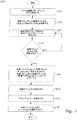
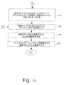
図7は、本発明の実施形態による、物理ブロックキャッシュの使用により物理ブロックドメインにおけるページのコンテンツを更新する1方法と関連する工程を示すプロセスフローチャートである。論理ページの更新を一時的に記憶するためにブロックキャッシュを用いるプロセス660は、工程670において開始し、ここで、ホストは、論理ブロック「A」の処理を開始する。換言すると、不揮発性メモリがインターフェース接続するシステム、または、不揮発性メモリが埋め込まれるシステムは、論理ブロック「A」のコンテンツへの更新の処理を開始し得る。
FIG. 7 is a process flowchart illustrating steps associated with one method of updating the content of a page in a physical block domain through the use of a physical block cache, according to an embodiment of the present invention. The
ホストが論理ブロック「A」の処理を開始した後、論理ブロック「A」にマッピングされるべき新しい物理ブロック「B」が工程672において取得される。その後、論理ブロック「A」に含まれるページへの更新が、コントローラによる例のように、工程674におけるブロックキャッシュに記憶される。図6aおよび図6bを参照して述べられたように、論理ブロック「A」にマッピングされる物理ブロック「A」がページの更新を収容し得ない場合、ページの更新は、キャッシュに記憶され得る。一旦論理ブロック「A」におけるページへの更新がブロックキャッシュに記憶されると、工程678において、ホストが例えば、論理ブロック「B」等の異なった論理ブロックの処理を開始する準備ができたか否かに関する判定が下される。すなわち、処理されることを必要とする論理ブロック「A」と関連する任意のさらなる更新の有無が判定される。
After the host has begun processing logical block "A", a new physical block "B" to be mapped to logical block "A" is obtained at
工程678における判定が、論理ブロック「B」の処理を開始するときではないという場合、論理ブロック「A」と関連するさらなる更新があることが示される。従って、プロセスフローは、工程674に戻り、ここで、論理ブロック「A」と関連更新がブロックキャッシュに記憶される。他方、論理ブロック「B」の処理を開始するときでないと判定された場合、物理ブロック「A」およびブロックキャッシュのコンテンツは、工程686において、物理ブロック「B」に組み合わされ得、従って、論理ブロック「A」と関連する最新コンテンツは、物理ブロック「B」に書き込まれる。すなわち、物理ブロック「A」のコンテンツ、および、ブロックキャッシュのコンテンツは、有効にマージされ、かつ、物理ブロック「B」に記憶され、従って、物理ブロック「B」は、論理ブロック「A」のページと関連する現在のコンテンツを含む。いくつかの場合において、ブロックキャッシュのコンテンツは、物理ブロック「A」のコンテンツを有効に奪い得、従って、実質的に、物理ブロック「A」のコンテンツが物理ブロック「B」にコピーまたは記憶されない。
If the determination in
論理ブロック「A」と関連する現在のコンテンツが物理ブロック「B」に書き込まれた後、物理ブロック「A」は、工程690において消去される。その後、工程694において、ブロックキャッシュが消去される。一旦ブロックキャッシュが消去されると、工程698において、物理ブロック「A」と論理ブロック「A」との関連がはずされる。物理ブロック「A」と論理ブロック「A」との関連をはずす工程は、マッピングを更新する工程を包含し得、これは、論理ブロック「A」が物理ブロック「B」と関連することを示す。物理ブロック「A」と論理ブロック「A」との関連がはずされた後、論理ブロックと関連するページの更新を一時的に記憶するためにブロックキャッシュを用いるプロセスが完了する。
After the current content associated with logical block "A" has been written to physical block "B", physical block "A" is erased at
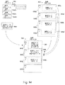
一般に、RAMキャッシュまたはブロックキャッシュが利用されることを可能にすることと関連する機能性が、例えば、プログラムコードデバイスとして、またはホストシステムへのファームウェアとして等ソフトウェアに提供される。本発明の実施形態によるホストシステムに提供されるソフトウェアまたはファームウェアと関連する適切なシステムアーキテクチャの1実施形態が図8に示される。システムアーキテクチャ700は、通常、アプリケーションインターフェースモジュール704、システムマネージャモジュール708、データマネージャモジュール712、データインテグリティマネージャ716およびデバイスマネージャならびにインターフェースモジュール720を含み得るがこれらに限定されない多様なモジュールを含む。一般に、システムアーキテクチャ700は、ソフトウェアコードデバイス、または、例えば、図3aのプロセッサ108等のプロセッサによってアクセスされ得るファームウェアを用いてインプリメントされ得る。
Generally, the functionality associated with allowing a RAM cache or block cache to be utilized is provided to software, for example, as a program code device or as firmware to a host system. One embodiment of a suitable system architecture associated with software or firmware provided to a host system according to embodiments of the present invention is shown in FIG. System architecture 700 typically includes a variety of modules, which may include, but are not limited to,
一般に、アプリケーションインターフェースモジュール704は、ホスト、オペレーティングシステムまたはユーザと直接的に通信するように構成され得る。アプリケーションインターフェースモジュール704は、さらに、システムマネージャモジュール708およびデータマネージャモジュール712とも通信する。ユーザがフラッシュメモリを読み出し、書き込みまたはフォーマット化することを所望する場合、ユーザは、オペレーティングシステムにリクエストを送信し、リクエストは、アプリケーションインターフェースモジュール704に渡される。アプリケーションインターフェースモジュール704は、リクエストに依存して、システムマネージャモジュール708またはデータマネージャモジュール712にリクエストを方向付ける。
In general,
システムマネージャモジュール708は、システム初期化サブモジュール724、消去カウントブロック管理サブモジュール726、および電力管理ブロックサブモジュール730を含む。システム初期化サブモジュール724は、通常、初期化リクエストが処理されることを可能にするように構成され、かつ、通常、消去管理サブモジュール726と通信する。
The
アプリケーションインターフェースモジュール704と通信することに加えて、システムマネージャモジュール708は、データマネージャモジュール712、ならびにデバイスマネージャおよびインターフェースモジュール720とも通信する。システムマネージャモジュール708およびアプリケーションインターフェースモジュール704の両方と通信するデータマネージャモジュール712は、ページまたはブロックマッピングを提供する機能性を含み得る。データマネージャモジュール712は、オペレーティングシステムおよびファイルシステムインターフェースレイヤと関連する機能性をさらに含み得る。
In addition to communicating with the
システムマネージャモジュール708、データマネージャ712およびデータインテグリティマネージャ716と通信するデバイスマネージャおよびインターフェースマネージャ720は、通常、フラッシュメモリインターフェースを提供し、かつ、例えば、I/Oインターフェース等のハードウェア抽象化と関連する機能性を含む。データインテグリティマネージャモジュール716は、機能性の中でもECCハンドリングを提供する。
The device manager and
本発明の1実施形態において、キャッシュが実質的にページ上で、実質的にページ単位で行われるようにブロックキャッシュを実行するのではなく、ブロックキャッシュは、グループ単位で実行され得る。同時係属中の米国特許出願第10/281,855号に記載されるように、グループは、ブロック内の任意の数のページを含む。例えば、32ページを含むブロックは、32ページが、それぞれが8ページの4つのグループにグループ分けされるように構成され得る。一般に、ブロックにおけるグループの数、およびグループにおけるページの数は様々である。 In one embodiment of the present invention, rather than performing the block cache such that caching is performed substantially on pages and substantially on a page basis, the block cache may be performed on a group basis. As described in co-pending US patent application Ser. No. 10 / 281,855, a group includes any number of pages within a block. For example, a block containing 32 pages may be configured such that 32 pages are grouped into 4 groups of 8 pages each. In general, the number of groups in a block and the number of pages in a group can vary.
グループ化スキーマが用いられた場合、更新データは、グループの一部分として物理ブロックに書き込まれ得る。図9aは、論理ブロック、物理ブロック、および本発明の実施形態によるグループに分割される新しい物理ブロックの概略図である。論理ブロック「A」900は、論理グループ904に分割され、これは、次に、各々が、多数の論理ページ908を含む。論理ブロック「A」900は、4つの論理グループ904を含むことが示され、これらの各々が、4つのページ908を含み、論理ブロック「A」900に含まれるグループ904およびページ908の数は様々であり得る。特定のページ908が属するグループ904は、通常、各ページ908と関連するオーバーヘッドまたは冗長領域において通常識別される。 If a grouping scheme is used, the update data may be written to a physical block as part of a group. FIG. 9a is a schematic diagram of logical blocks, physical blocks, and new physical blocks that are divided into groups according to an embodiment of the present invention. Logical block "A" 900 is divided into logical groups 904, which, in turn, each include a number of logical pages 908. Logical block "A" 900 is shown to include four logical groups 904, each of which includes four pages 908, and the number of groups 904 and pages 908 included in logical block "A" 900 varies. Can be The group 904 to which a particular page 908 belongs is typically identified in the overhead or redundant area associated with each page 908.
物理ブロック「B」912は、論理ブロック「A」900と関連付けられ、従って、物理ブロック「B」912は、論理ブロック「A」900と関連するデータまたはコンテンツを含む。示されるように、物理ページ(図示せず)を含む、物理ブロック「B」912の第1の物理グループ916aは、論理グループ904aと関連するデータ920aを含む。同様に、第2の物理グループ916bは、論理グループ904bと関連するデータ920bを含み、第3の物理グループ916cは、論理グループ904cと関連するデータ920cを含み、第4の物理グループ916dは、論理グループ904dと関連するデータ920dを含む。
Physical block "B" 912 is associated with logical block "A" 900, so physical block "B" 912 contains data or content associated with logical block "A" 900. As shown, a first
論理グループ904bと関連するデータが更新されるべきことを示す更新924が、例えば、ホストから受信された場合、更新924がデータ920bと有効にマージされ、かつ、新しい物理ブロック「B1」928における第1の利用可能なグループ932aに記憶される。マージは、論理グループ904bの各ページと関連する最新コンテンツがグループ932aに記憶されることを可能にするように行われる。更新されたグループと関連するデータおよびもとのデータのマージは、図10を参照して後述される。図9bに示されるように、論理ブロック「A」900と関連する更新プロセスが完了した場合、物理ブロック「B1」928は、論理ブロック「A」900と関連する物理ブロックになり得、すなわち、物理ブロック「B1」928は、論理ブロック「A」900と関連するようになり得る一方で、物理ブロック「B」912は、論理ブロック「A」900との関連がはずされる。
If an
物理ブロック「B」912と論理ブロック「A」900との関連がはずされる前に、物理ブロック「B」912のコンテンツは物理ブロック「B1」928にマージされていない。例えば、第1の論理グループ904aと関連するデータ920bは、コピーされるか、そうでない場合、物理ブロック「B1」928の第2の物理グループ932bに提供される一方で、第3の論理グループ904cと関連するデータ920cは、第3の物理グループ932cに提供される。同様に、第4の論理グループ904dと関連するデータ920dは、第4の物理グループ932dに提供され得る。その結果、論理ブロック「A」900と関連する最新コンテンツが物理ブロック「B1」928に存在する。
Before the physical block “B” 912 and the logical block “A” 900 are dissociated, the contents of the physical block “B” 912 have not been merged into the physical block “B1” 928. For example,
物理ブロック「B1」928が論理ブロック「A」900と関連する物理ブロックになった後、論理ブロック「A」900にさらなる更新がなされ得る。図9cを参照して、予め更新され、かつ、グループ904に分割される論理ブロック「A」900へのさらなる更新を処理するプロセスが本発明の実施形態により記載される。論理グループ904bと関連する新しい更新940が処理されるべき場合、物理ブロック「B」912は、論理ブロックと関連する最新コンテンツをもはや含まず、物理ブロック「B1」928が有効に一杯であるので、更新940を記憶するために新しい物理ブロック「B2」944が取得され得る。特に、物理グループ932aに記憶される論理グループ904bと関連するデータ936は、更新940とマージされ、かつ、物理ブロック「B2」944の第1の利用可能なグループ946aに更新データ948として記憶される。更新データ948は、論理グループ904b内のページと関連する最新コンテンツを含む。
After physical block “B1” 928 becomes the physical block associated with logical block “A” 900, further updates may be made to logical block “A” 900. With reference to FIG. 9c, a process for processing further updates to a logical block “A” 900 that has been previously updated and divided into groups 904 is described according to an embodiment of the present invention. If a
一旦更新プロセスが完了すると、論理ブロック「A」900と関連する最新データは、物理ブロック「B2」944に提供され得る。例示的に、第1の論理グループ904aと関連するデータ920aが物理ブロック「B2」944の第2の物理グループ946bに提供され得、第3の論理グループ904cと関連するデータ920cが第3の物理グループ946cに提供され得、かつ、第4の論理グループ904dと関連するデータ920dは、第4の物理グループ946dに提供され得る。物理ブロック「B2」944が論理ブロック「A」900と関連する最新コンテンツを含む場合、物理ブロック「B2」944は、論理ブロック「A」900と関連付けられ得る一方で、物理ブロック「B1」928は、論理ブロック「A」900との関連がはずされ得る。
Once the update process is complete, the latest data associated with logical block "A" 900 may be provided to physical block "B2" 944. Illustratively,
グループに分割される物理ブロックが、最初、コンテンツを有さない場合、論理ブロックと関連する新しいか、または更新されたデータが受信されると、ホストからの例について言えば、データのいくつかが、物理ブロックに記憶される他のデータを有効に奪う場合であっても、新しいか、または更新されたデータが物理ブロックに記憶され得る。図9dは、グループに分割された論理ブロックと、論理ブロックに関連付けられた更新データを含む論理ブロックと、本発明の実施形態による論理ブロックに関連付けられる最新のデータとを含む新しい物理ブロックの概略図である。コンテンツが論理ブロック「A」950と関連させられるべきときに、論理ブロック「A」950が、最初、コンテンツを含まない場合、そのコンテンツは、論理ブロック「A」950と関連する物理ブロック「B」956に書き込まれ得る。示されるように、論理ブロック「A」950の第2の論理グループ952bと関連する新しいデータ960aが提供された場合、データ960aは、物理ブロック「B」956の第1の利用可能な物理グループ958aに記憶され得る。
If the physical blocks that are divided into groups initially have no content, and when new or updated data associated with a logical block is received, some of the data, for example from the host, However, new or updated data may be stored in the physical block even if it effectively steals other data stored in the physical block. FIG. 9d is a schematic diagram of a new physical block including a logical block divided into groups, a logical block including update data associated with the logical block, and the latest data associated with the logical block according to an embodiment of the present invention. It is. When content is to be associated with logical block "A" 950, if logical block "A" 950 initially does not contain content, then the content is physical block "B" associated with logical block "A" 950. 956. As shown, if
第2の論理グループ952bと関連するデータが更新された場合、更新データ960a’は、例えば、第2の物理グループ958b等の、次の利用可能な物理グループ958に記憶され得る。データ960a’が記憶された後、第3の論理グループ952cと関連する新しいデータ960bが受信された場合、データ960bは、次の利用可能な物理グループ958すなわち、第3の物理グループ958cに記憶される。最後に、第2の論理グループ952bと関連する更新データ960a’’が受信された場合、更新データ960a’’は、記載された実施形態において、物理ブロック「B」956において利用可能な最後の物理グループ958である第4の物理グループ958dに記憶される。
If the data associated with the second logical group 952b has been updated, the updated
一旦物理ブロック「B」956が一杯であると、すなわち、一旦物理ブロック「B」956内のすべてのグループがデータ960を含み、論理ブロック「A」950と関連する新しいか、または更新されたデータが受信されると、通常、使用する新しい物理ブロックが取得される。例示的に、論理グループ952dの新しいデータ966が受信される場合、データ966を収容するための新しい物理ブロック「B1」962が取得され得る。データ966は、物理ブロック「B1」962における第1の利用可能なグループ964aに記憶され得る。データ966が記憶された後、物理ブロック「B」956に含まれるデータ960は、物理ブロック「B2」962に記憶され得る。
Once physical block "B" 956 is full, i.e., once all groups in physical block "B" 956 contain data 960, new or updated data associated with logical block "A" 950 Is received, a new physical block to be used is usually obtained. Exemplarily, when new data 966 of the logical group 952d is received, a new physical block “B1” 962 for accommodating the data 966 may be obtained. Data 966 may be stored in a first
物理ブロック「B」956に含まれるデータ960を物理ブロック「B」962に記憶するために、グループ958は、「後から先(bottom first)」の態様で、すなわち、グループ958dから開始してグループ958aで終了するように、物理ブロック「B」956から読み出され得る。データが、論理グループ952bと関連するデータ960を含む物理グループ958a、958b、958d内の同じページオフセットにて存在する場合、物理グループ958dにおけるページオフセットにて含まれるデータは、最新データであると判断される。一般に、物理グループの数が高いほど、同グループのデータは新しい。一旦論理グループ952bと関連する最新データが識別されるか、または、一旦データ960a、データ960a’およびデータ960a’’が適切にマージされると、マージされ、論理グループ952bと関連する更新されたデータ968は、物理ブロック「B1」962内のグループ964bに記憶される。実質的に、物理ブロック「B」956内のただ1つのグループ958cが、論理グループ952dと関連するデータ960bを含むので、データ960bは、物理ブロック「B1」962の第3のグループ964cに提供され得る。グループ964dにはデータが記憶されないので、グループ964dは、例えば、論理グループ952a等の新しい論理グループと関連するデータを収容するために有効に利用可能である。
In order to store the data 960 contained in the physical block “B” 956 in the physical block “B” 962, the group 958 is configured in a “bottom first” manner, that is, starting from the
上述のように、論理グループのための更新データが受信されると、そのグループのより古いデータが存在する場合、そのより古いデータは、適宜、更新データとマージされ得る。1実施形態において、更新データは、グループ内の実質的に各ページの更新データを含む場合、更新データは、すべてのより古いデータを有効に上書きする。しかしながら、更新データがグループ内のいくつかのページのみへの更新を含む場合、マージプロセスが行われ得る。次に図10を参照して、もとのデータのグループを新しいデータのグループとマージする1方法が、本発明の実施形態により説明される。グループ「X」1000は、8ページ1002を含み得る。いくつかのページ1002は、データを含み得る一方で、他のページ1002は、実質的に空であり得る。示されるように、ページ1002a、1002d、1002eは、もとのデータを含む。
As described above, when update data for a logical group is received, older data for that group, if any, may be merged with the update data, as appropriate. In one embodiment, if the update data includes update data for substantially each page in the group, the update data effectively overwrites all older data. However, if the update data includes updates to only some of the pages in the group, a merge process may occur. Referring now to FIG. 10, one method of merging an original group of data with a new group of data is described according to an embodiment of the present invention. Group “X” 1000 may include eight pages 1002. Some pages 1002 may contain data, while other pages 1002 may be substantially empty. As shown,
グループ「X」1000の新しいデータが、更新の形態でホストから受信された場合、新しいデータは、グループ更新1006のページ1008にて提供され得る。ページ1008a〜dおよびページ1008gは、グループ「X」1000に含まれるデータとマージされるべき新しいか、または更新されたデータを含む。マージプロセスは、通常、グループ「X」1000と関連する最新データを識別する工程を含む。新しいデータがもとのデータを有効に上書きするので、新しいデータは、グループ「X」1000と関連する最新データであると考えられる。他方、もとのデータを有効に上書きする新しいデータがない場合、もとのデータは、最新データであると考えられ得る。
If new data for group "X" 1000 is received from the host in the form of an update, the new data may be provided on
グループ「X」1000のもとのデータを更新1006のグループとマージした結果を含むマージされたデータ1010は、ページ1012を含み、従って、グループ「X」1000の第1のページ1002に対応する第1のページ1012aは、ページ1008aからの新しいデータを含む。なぜなら、ページ1008aからの新しいデータは、第1のページ1002において記憶されるもとのデータを有効に奪うからである。本来、データがページ1002b、1002cに含まれないので、ページ1008b、1008cが提供された新しいデータは、ページ1012b、1012cにそれぞれ書き込まれる。ページ1008dに含まれるデータは、ページ1002dに含まれるデータよりも最新であるので、ページ1012dは、ページ1008dからの新しいデータを含む。更新1006のグループは、ページ1008eにおいて更新されたコンテンツが含まれなかったので、ページ1012eは、ページ1002eからのもとのデータを含む。最後に、ページ1012gは、ページ1008gに含まれる新しいデータを含む。一旦マージされたデータ1010が完了すると、マージされたデータ1010は、有効にグループ「X」1000になる。
一般に、グループへの更新が特定のページと関連するデータを含む場合、データは、生じたグループのマージされたデータ内の対応するページに含まれる。なぜなら、このデータは、特定のページと関連する唯一のデータであるか、またはそのデータは、特定のページと関連するもとのデータを上書きするからである。あるいは、所与のページのもとのデータが、ページを含むグループへの更新によって上書きされない場合、もとのデータは、グループの結果として生じるマージされたデータ内で対応するページに含まれる。 Generally, if an update to a group includes data associated with a particular page, the data will be included on the corresponding page in the merged data of the resulting group. This is because this data is the only data associated with a particular page, or that data overwrites the original data associated with a particular page. Alternatively, if the original data for a given page is not overwritten by updates to the group containing the page, the original data is included in the corresponding page in the resulting merged data for the group.
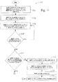
図11aおよび図11bは、本発明の実施形態によるグループに分割される論理ブロックと関連するコンテンツを更新する1方法と関連する工程を示すプロセスフローチャートである。コンテンツを更新するプロセス1100は、工程1102にて開始し、ここで、物理ブロック「B」と関連する、論理ブロック「A」のグループ「X」と関連するコンテンツは、例えば、ホストによって更新される。通常、論理グループ「X」は、2つ以上のページを含む。一旦論理グループ「A」のグループ「X」と関連するコンテンツが更新されると、新しい物理ブロック「B1」が取得されて、工程1104において論理ブロック「A」と関連付けられる。
11a and 11b are process flowcharts illustrating steps associated with one method of updating content associated with logical blocks that are divided into groups according to an embodiment of the present invention. The process of updating
工程1106において、通常、物理ブロック「B」内のグループに記憶される、論理グループ「X」と関連する古いコンテンツは、論理グループ「X」の新しいか、または更新されたコンテンツとマージされ、かつ、物理ブロック「B1」に記憶される。マージされたコンテンツが物理ブロック「B1」に記憶された後、工程1108において、記憶されるべき論理ブロック「A」のより新しいか、または更新されたコンテンツの有無に関する判定が下される。記憶されるべき、新しいか、または更新されたさらなるコンテンツがあると判定された場合、プロセスフローは、工程1105に戻り、ここで、論理ブロック「A」内の異なった論理グループであり得る論理グループ「X」と関連する古いコンテンツは、新しいか、または更新されたコンテンツとマージされる。換言すると、新しいか、または更新されたコンテンツは、論理ブロック「A」内の実質的に任意の論理グループと関連付けられ得、従って、このマージは、新しいか、または更新されたコンテンツと適切な論理グループとの間で生じる。
In
あるいは、工程1108において、論理ブロック「A」の新しいか、または更新されたコンテンツがもはや記憶されないことが判定された場合、工程1110において、物理ブロック「B」の物理ブロック「B1」にマージされなかったコンテンツ等の、残りのコンテンツを記憶するための十分な空間が物理ブロック「B1」内に有るか否かに関する判定が下される。すなわち、論理ブロック「A」と関連する現在のコンテンツの全部の物理的表現(full physical representation)が物理ブロック「B」に記憶され得るか否かが判定される。物理ブロック「B」の残りのコンテンツを物理ブロック「B1」に記憶するために、物理ブロック「B1」において利用可能なグループが十分にあると判定された場合、工程1120において、物理ブロック「B」からの残りのコンテンツは、物理ブロック「B1」にコピーされる。
Alternatively, if it is determined in
物理ブロック「B」からの残りのコンテンツが物理ブロック「B1」にコピーされた後、物理ブロック「B1」は、論理ブロック「A」と関連する最新コンテンツまたは現在のコンテンツを含む。従って、物理ブロック「B」は、工程1122において消去され、かつ、工程1124において論理ブロック「A」との関連がはずされる。一旦物理ブロック「B」と論理ブロック「A」との関連が外されると、論理ブロックと関連するコンテンツを更新するプロセスが完了する。
After the remaining content from physical block “B” has been copied to physical block “B1”, physical block “B1” contains the latest or current content associated with logical block “A”. Accordingly, physical block "B" is erased in
工程1110に戻って、物理ブロック「B」の残りのコンテンツを記憶するために物理ブロック「B1」において利用可能なグループが十分にないと判定された場合、新しい物理ブロックが取得されて、「論理ブロック「A」と関連する最新コンテンツを含むことが示される。従って、プロセスフローは、工程1112に進み、ここで、新しい物理ブロック「B2」が論理ブロック「A」と関連付けられるように割り当てられる。一旦新しい物理ブロック「B2」が取得されると、物理ブロック「B」および物理ブロック「B1」のコンテンツが工程1114において物理ブロック「B2」にマージされ、従って、論理ブロック「A」と関連する最新コンテンツは物理ブロック「B2」に記憶される。一般に、物理ブロック「B」および物理ブロック「B1」のコンテンツをマージする工程は、物理ブロック「B」および物理ブロック「B1」内のグループのコンテンツをマージする工程を包含する。 Returning to step 1110, if it is determined that there are not enough groups available in physical block "B1" to store the remaining content of physical block "B", a new physical block is obtained and a "logical It is shown to include the latest content associated with block "A". Accordingly, process flow proceeds to step 1112, where a new physical block "B2" is assigned to be associated with logical block "A". Once the new physical block "B2" is obtained, the contents of physical block "B" and physical block "B1" are merged into physical block "B2" in step 1114, and thus the latest associated with logical block "A". The content is stored in the physical block “B2”. In general, merging the contents of physical block “B” and physical block “B1” involves merging the contents of physical block “B” and the groups within physical block “B1”.
コンテンツが物理ブロック「B2」にマージされた後、物理ブロック「B1」は、工程1116において消去される。一旦物理ブロック「B1」が消去されると、物理ブロック「B1」と論理ブロック「A」との関連は、工程1118においてはずされる。その後、プロセスフローは、工程1122に進み、ここで、物理ブロック「B」は消去される。 After the content has been merged into physical block “B2”, physical block “B1” is erased in step 1116. Once physical block "B1" is erased, physical block "B1" and logical block "A" are dissociated in step 1118. Thereafter, the process flow proceeds to step 1122, where physical block "B" is erased.
上述のRAMキャッシュは、論理グループと関連する更新のグループをキャッシュするために用いられ得る。RAMキャッシュの使用は、通常、論理ブロックと関連する更新プロセスの進行中に必要とされる消去プロセスの数を低減し得る。なぜなら、RAMキャッシュは、更新プロセスが完了するまで更新され、その時点にて、新しい物理ブロックが取得されて、論理ブロックと関連する最新データを記憶し、かつ古い物理ブロックが消去され得るからである。 The RAM cache described above can be used to cache groups of updates associated with logical groups. The use of a RAM cache may typically reduce the number of erase processes required during the progress of the update process associated with a logical block. This is because the RAM cache is updated until the update process is completed, at which point a new physical block may be obtained, store the latest data associated with the logical block, and the old physical block may be erased. .
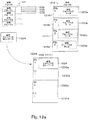
図12aを参照して、グループに有効に分割されるRAMキャッシュの使用が、本発明の実施形態により説明される。論理ブロック「A」1200は、論理グループ1204に分割され、その後、各々が多数の論理ページ1208を含む。物理ブロック「B」1212は、論理ブロック「A」1200と関連付けられ、従って、物理ブロック「B」1212は、論理ブロック「A」1200と関連するデータまたはコンテンツを含む。示されるように、物理ブロック「B」1212の物理ページ(図示せず)を含む第1の物理グループ1216aは、論理グループ1204aと関連するデータ1220aを含む。同様に、第2の物理グループ1216bは、論理グループ1204bと関連するデータ1220bを含み、第3の物理グループ1216cは、論理グループ1204cと関連するデータ1220cを含み、かつ、第4の物理グループ1216dは、論理グループ1204dと関連するデータ1220dを含む。
With reference to FIG. 12a, the use of a RAM cache that is effectively divided into groups is described according to an embodiment of the present invention. Logical block "A" 1200 is divided into logical groups 1204, each thereafter comprising a number of logical pages 1208. Physical block "B" 1212 is associated with logical block "A" 1200, so physical block "B" 1212 includes data or content associated with logical block "A" 1200. As shown, a first
ホストによる例のように、論理グループ1204bと関連するデータが更新されるべきであることを示す更新1224が受信されると、更新1224は、RAMキャッシュ1228内の第1の利用可能なグループ1232aに記憶される。あるいは、1実施形態において、更新1224が第2の論理グループ1204bと関連付けられるので、更新1124は、第2のRAMグループ1232bに記憶され得る。
When an
論理グループ1204bと関連するデータが再び更新されるべきことを示すさらなる更新が受信される場合、このような更新は、RAMキャッシュ1228内のグループ1232aのコンテンツとマージされ得る。図12bに示されるように、論理グループ1204bに対応する新しい更新1236が受信される場合、新しい更新1236におけるデータは、RAMグループ1232aに予め記憶されたコンテンツとマージされ得、論理グループ1204bと関連するマージされ、更新されたデータ1224’を形成する。いくつかの例において、新しい更新されたデータ1236のいくつかは、マージプロセスの間、前の更新されたデータ、すなわち、図12aの新しいデータ1224を上書きし得る。なぜなら、RAMが上書きされ得るからである。
If further updates are received indicating that data associated with logical group 1204b should be updated again, such updates may be merged with the contents of
論理グループ1204dの更新1240の場合、更新1240は、次の利用可能なRAMページ1232bに記憶され得る。更新1240が更新1236の前に受信されるか、後に受信されるかに関わらず、更新1236は、依然として、グループ1232aに組み込まれ、かつ更新1240はグループ1232bに記憶されることが理解されるべきである。
For a
一旦論理ブロック「A」1200になされるべき実質的にすべての更新が完了すると、すなわち、別の論理ブロックが更新されるべきときである場合、RAMキャッシュ1228のコンテンツおよび物理ブロック「B」1212のコンテンツが新しい物理ブロックにマージされ得る。図12cは、本発明の実施形態により、RAMキャッシュ1228および物理ブロック「B」1212が新しい物理ブロックにマージされた後の、論理ブロック「A」1200および新しい物理ブロックの概略図である。一旦論理ブロック「A」1200になされるべき更新が完了したことが判定されると、物理ブロック「B1」1236が、通常、取得される。一旦物理ブロック「B1」1236が取得されると、図10を参照して説明された例のように、RAMキャッシュ1228のグループ1232のコンテンツは、物理ブロック「B」1212のグループ1220のコンテンツとマージされ得、そして、物理ブロック「B1」1236に記憶され得る。
Once substantially all updates to be made to logical block “A” 1200 have been completed, ie, when another logical block is to be updated, the contents of
論理グループ1204bと関連するデータがRAMキャッシュ1228内で更新されたので、更新データ1224’は、論理グループ1204bと関連付けられたもとのデータを表すデータ1220bとマージされる。データ1220bは、論理グループ1204と関連するいくつかの現在のコンテンツを含み得るか、または、データ1220bは、更新されたデータ1224’からみて有効に古くなり(outdated)得ることが理解されるべきである。論理グループ1204bと関連する最新または現在のデータが物理ブロック「B1」1236において表されることを実質的に保証するために、更新されたデータ1224’およびデータ1220bからマージされたデータ1244を生成するためにマージプロセスが用いられる。同じ論理グループ1204と関連する同じページオフセットが、対応する物理グループ1216内にさらなるデータを含む場合、RAMキャッシュ1228のRAMグループ1232に含まれるデータは、通常、マージされたデータに含まれる。すなわち、論理グループ1204内のページオフセットに対応するデータが、物理グループ1216およびRAMグループ1232の両方に存在する場合、RAMグループ1232におけるデータは、マージされたデータに含まれる。なぜなら、RAMグループ1232におけるデータはより最近のものだからである。
Because the data associated with logical group 1204b has been updated in
記載された実施形態において、論理グループ1204aと関連するもとのデータであるデータ1220aが物理グループ1240aに記憶された後、マージされたデータ1244が第2の物理グループ1240bに記憶され得る。論理グループ1204cと関連するデータ1220cは、更新されなかったので、データ1220cは、物理グループ1240cに記憶され得る。論理グループ1204dが、物理ブロック「B」1212の物理グループ1216dに記憶される関連するもとのデータ1220d、および、RAMキャッシュ1228のRAMグループ1232bに記憶される、新しいか、または更新されたデータ1240を有する。従って、マージプロセスがデータ1220dおよび、新しいか、または更新されたデータ1240を用いて実行され、論理グループ1204dと関連する最新または現在のコンテンツを表すマージされたデータ1248を生成する。示されるように、マージされたデータ1248は、物理グループ1240dに記憶される。従って、物理ブロック「B」1212は、古くなり、かつ、消去され得、ならびに、論理ブロック「A」1200との関連がはずされる。なぜなら、物理ブロック「B1」1236は、ここで、論理ブロック「A」1200と関連する現在のコンテンツを含むからである。
In the described embodiment, after
図12dは、論理ブロック1200、物理ブロック1212およびRAMキャッシュ1228の概略図であり、ここで、RAMキャッシュのコンテンツが存在する。なぜなら、本発明の実施形態により、新しいデータを収容するための十分な空間が物理ブロック内にないからである。物理ブロック1212のグループ1216は、従って、グループ1216aが論理グループ1204bと関連するもとのデータ1220aを含み、グループ1216bが論理グループ1204bと関連する更新データ1220a’を含み、グループ1216cが、論理グループ1204cと関連するデータ1220cを含み、そして、グループ1216dが論理グループ1204dと関連するデータ1220a’’を含むというふうである。従って、データが書き込まれ得る利用可能なさらなるグループ1216がない物理ブロック1212は一杯である。
FIG. 12d is a schematic diagram of a
論理グループ1204dに対応する新しいデータ1240が提供される場合、新しいデータ1240は、RAMキャッシュ1228における適切なRAMグループ1232に記憶される。1実施形態において、適切なRAMグループ1232は、RAMキャッシュ1228内で最初に利用可能なRAMグループ1232aであり得る。論理ブロック「A」1200になされるべきさらなる更新がないと判定された場合、論理ブロック「A」1200と関連付けられる新しい物理ブロック「B1」1252が取得され得る。
If
物理ブロック「B1」1252内で、第1の物理グループ1260は、論理グループ1204bと関連するマージされたデータ1260を含む。マージされたデータ1260は、データ1220a、データ1220a’、およびデータ1220a’’をマージすることによって生成され、従って、論理グループ1204bと関連する最新データは、マージされたデータ1260において含まれる。論理グループ1204bと関連する最新データがマージされたデータ1260に含まれることを実質的に保証するために、グループ1216は、グループ1216dで開始し、かつグループ1216aで終了して処理され、従って、最新データは、所与の論理グループと関連する特定のページオフセットに含まれる。
Within physical block “B1” 1252, first
一旦マージされたデータ1260が生成され、かつ、グループ1256aに記憶されると、論理グループ1204cと関連するデータ1220cは、グループ1256bに記憶され、RAMキャッシュ1228に存在するデータ1240はグループ1256に記憶される。その結果、物理ブロック「B1」1252は、論理ブロック「A」1200と関連する最新データを含む。
Once merged
図13を参照して、論理ブロックの論理グループと関連する更新を記憶するためにRAMキャッシュを用いる1方法と関連する工程が本発明の実施形態により記載される。プロセス1300は、工程1304にて開始し、ここで、ホストは、物理ブロック「B」と関連する論理ブロック「A」を処理することを開始する。論理ブロック「A」を処理する工程は、通常、論理ブロック「A」内の論理グループの更新を処理する工程を包含する。
Referring to FIG. 13, one method of using a RAM cache to store updates associated with logical groups of logical blocks is described in accordance with an embodiment of the present invention.
工程1308において、RAMキャッシュはクリアされる。一旦RAMキャッシュがクリアされると、論理ブロック「A」と関連する更新されたコンテンツは、工程1312において、RAMキャッシュに記憶される。特に、更新されたコンテンツは、更新されたコンテンツが関連付けられる論理グループに基づいて、適切なRAMグループに記憶され得る。その後、工程1316において、記憶されるべき論理ブロック「A」と関連する更新されたさらなるコンテンツの有無が判定される。記憶するさらなるコンテンツがあることが判定された場合、プロセスフローは工程1312に戻り、ここで、更新されたコンテンツは記憶される。
In
あるいは、工程1312において、論理ブロック「A」の更新されたさらなるコンテンツがないと判定された場合、新しい物理ブロック「B1」は、工程1320において、論理ブロック「A」と関連付けられるように割り当てられる。換言すると、論理ブロック「A」と関連する最新データが書き込まれるべき物理ブロック「B1」が取得される。一旦新しい物理ブロック「B1」が割り当てられると、RAMキャッシュのコンテンツおよび物理ブロック「B」のコンテンツは、工程1324において、物理ブロック「B1」に、適宜、マージされる。コンテンツをマージする工程は、通常、各論理グループと関連するコンテンツをマージする工程を含み得、従って、マージされたコンテンツは、各論理グループと関連する最新または現在のコンテンツである。
Alternatively, if it is determined in
一旦RAMキャッシュのコンテンツおよび物理ブロック「B」のコンテンツがマージされると、物理ブロック「B1」は、論理ブロック「A」と関連する最新コンテンツを有効に含む。従って、工程1328において、物理ブロック「B」は消去され得る。物理ブロック「B」が消去された後、物理ブロック「B」と論理ブロック「A」との関連がはずされ、かつ、更新を記憶するためにRAMキャッシュを用いるプロセスが完了する。
Once the contents of the RAM cache and the contents of physical block "B" are merged, physical block "B1" effectively contains the latest content associated with logical block "A". Accordingly, in
いくつかの場合、例えば、利用可能なRAMがシステム内に十分にない場合の例のように、RAMキャッシュの使用は可能になり得ない。RAMキャッシュが用いられない場合、キャッシュブロックまたはブロックキャッシュが、その代わりに、論理ブロックと関連するグループへの更新を記憶するために用いられ得る。図14aは、グループに有効に分割され、かつ、本発明の実施形態により、グループに分割される論理ブロックと関連する更新を記憶する際に用いるために適切であるRAMキャッシュの概略図である。論理ブロック「A」1400は、論理グループ1404に分割され、その後、各々は、多数の論理ページ1408を含む。物理ブロック「B」1412は、論理ブロック「A」4200と関連し、従って、物理ブロック「B」1412は、論理ブロック「A」1400と関連するデータを含む。物理ページ(図示せず)を含む物理ブロック「B」1412の第1の物理グループ1416aは、論理グループ1404aと関連するデータ1420aを含む。同様に、第4の物理グループ1416dは、論理グループ1404bと関連する更新データ1420dを含む。第2の物理グループ1416bは、論理グループ1404aと関連するデータ1420bを含み、第3の物理グループ1416cは、論理グループ1204cと関連するデータ1420cを含む。物理ブロック「B」1412は、論理グループ1404dと関連する任意のデータを含まない。
In some cases, the use of a RAM cache may not be possible, for example, as in the case where there is not enough RAM available in the system. If a RAM cache is not used, a cache block or block cache may be used instead to store updates to the group associated with the logical block. FIG. 14a is a schematic diagram of a RAM cache that is effectively divided into groups and that is suitable for use in storing updates associated with logical blocks that are divided into groups according to embodiments of the present invention. Logical block "A" 1400 is divided into
論理グループ1404dと関連するデータを含む更新1424が受信され、更新1424は、物理ブロックキャッシュ1428内の第1の利用可能なグループ1432aに記憶される。論理グループ1404dと関連するデータが再び更新されるべきことを示すさらなる更新が受信される場合、このような更新は、ブロックキャッシュ1428内の、次の利用可能なグループ1432bに記憶され得る。図14bに示されるように、論理グループ1404dに対応する新しい更新1426が受信されると、新しい更新1426におけるデータは、グループ1432bに記憶される。1実施形態において、データ1424およびデータ1426の両方に含まれる論理グループ1404dと関連する特定の現在のデータがあり得ることが理解されるべきである。しかしながら、情報のページがデータ1426に存在すると、データ1424における対応するページが、さらに情報を含む場合、データ1426におけるその情報は、通常、論理グループ1404dと関連する最近のデータが必要とされる場合に用いられる。
An
図14cは、論理ブロック、すなわち、図14bの論理ブロック「A」1400、ならびに、ブロックキャッシュのコンテンツ、および論理ブロックと関連するもとの物理ブロック(すなわち、図14bのブロックキャッシュ1428および物理ブロック「B」1412)が、本発明の実施形態による新しい物理ブロックにマージされた後の新しい物理ブロックの概略図である。新しい物理ブロック「B1」1440が取得され得、論理ブロック「A」1400になされるべき更新が本質的にもはやない場合論理ブロック「A」1400と関連付けられる。論理ブロック「A」1400と関連する更新が完了した場合、ブロックキャッシュ1428内で利用可能なグループ1432c、1432dが有効に空になり、かつ、新しいか、または異なった論理ブロック、論理ブロック「A」1400の論理グループと関連するデータを記憶するために後からさえも利用可能であることが理解されるべきである。
FIG. 14c illustrates the logical block, ie, logical block “A” 1400 of FIG. 14b, and the contents of the block cache and the original physical block associated with the logical block (ie,
図10に示される例のように、一旦新しい物理ブロック「B1」1440が取得されると、論理グループ1404bと関連付けられるデータ1420aおよびデータ1420dがマージされ、新しい物理ブロック「B1」1440のグループ1444aに記憶され得るマージされたデータ1446を形成する。データ1420bは、グループ1416bからグループ1444bにコピーされ得、データ1420cは、グループ1416cからグループ1444cにコピーされ得る。
As in the example shown in FIG. 10, once a new physical block “B1” 1440 is obtained, the
ブロックキャッシュ1428は、論理グループ1404dと関連付けられるデータ1424およびデータ1426を含むので、データ1424およびデータ1426はマージされて、新しい物理ブロック「B1」1440の物理グループ1444dに記憶されるマージされたデータ1448を形成する。マージされたデータ1448は、通常、論理グループ1404dと関連する最新または現在のコンテンツを含む。一旦新しい物理ブロック「B1」1440が占有されると、新しい物理ブロック「B1」1440は、論理ブロック「A」1400と関連する最新または現在のコンテンツを有効に含む。従って、物理ブロック「B」1412は、実質的に古くなり、かつ、消去され得、および論理ブロック「A」1400との関連がはずされ得る。
Since
上述のように、ブロックキャッシュ1428は利用可能なグループ1432を含む。このグループは、次の更新プロセスの進行中に、異なった論理ブロックまたは論理ブロック「A」1400と関連する更新または新しいデータを記憶するために用いられ得る。図14dを参照して、論理ブロック「A」1400と関連する新しい更新を記憶するための、ブロックキャッシュ1428内で利用可能なグループ1432c、1432dの使用が本発明の実施形態により説明される。ブロックキャッシュ1428内のグループ1432a、1432bのコンテンツは、実質的に任意の論理ブロックと関連する古いコンテンツであり得、かつ、論理ブロック「A」1400と関連する古いコンテンツであることに限定されないことが理解されるべきである。通常、グループ1432a、1432bの古いコンテンツは、異なった論理ブロックと関連付けられる。
As described above,
論理グループ1404dと関連付けられる更新が受信される場合、更新のコンテンツは、論理グループ1404dに対応し、かつ、物理ブロック1412’の物理グループ1416a’に記憶される先行するデータ1422aとマージされ得る。論理グループ1404dと関連付けられるマージされたデータ1450は、その後、ブロックキャッシュ1428内の第1の利用可能なグループ1432cに記憶され得る。同様に、論理グループ1404bと関連する更新が受信された場合、更新のコンテンツは、論理グループ1404bに対応する物理グループ1416c’に記憶された前のデータ1422cとマージされ得る。
If an update is received that is associated with
論理ブロック「A」1400と関連するさらなる情報がキャッシュされる必要がある場合、ブロックキャッシュ1428が一杯なので、新しいブロックキャッシュが取得され得る。次に、図14eを参照して、論理ブロック「A」1400と関連する更新を記憶する2つのブロックキャッシュの使用が本発明の実施形態により記載される。新しいか、または現在のブロックキャッシュ1464は、ブロックキャッシュ1428が一杯であり、かつ、論理ブロック「A」1400への更新が受信されると取得され得る。例えば、論理グループ1404cと関連する更新が受信された場合、更新と関連するデータは、グループ1416b’に含まれるデータ1422bとマージされ得る。なぜなら、データ1422bは、さらに、論理グループ1404cと関連付けられるからである。一旦マージされたデータ1460が生成されると、マージされたデータ1460は、現在のブロックキャッシュ1464における第1の利用可能グループ1468に記憶され得る。
If more information associated with logical block "A" 1400 needs to be cached, a new block cache may be obtained because
一般に、現在のキャッシュブロック1464は、現在のキャッシュブロック1464が利用可能なグループをもはや有しなくなるまで、適宜、更新、またはマージされた更新を記憶するために用いられ得る。現在のキャッシュブロック1464が一杯であり、かつ、論理ブロック「A」1400と関連する更新がさらに必要とされる場合、新しい現在のキャッシュブロックが取得され得る。
In general, the
マージされたデータ1460が第1の利用可能なグループ1468に記憶された後、論理ブロック「A」1400と関連する更新がもはやない場合、物理ブロック「B」1412’およびブロックキャッシュ1428のコンテンツを現在のブロックキャッシュ1464にマージすることが可能か否か、または、物理ブロック「B」1412’、ブロックキャッシュ1428および現在のブロックキャッシュ1464のコンテンツが新しい物理ブロックにマージされるべきか否かが判定され得る。示されるような実施形態において、物理ブロック「B」1412’およびブロックキャッシュ1428のコンテンツを現在のブロックキャッシュ1464にマージすることが可能である。図14fは、ブロックキャッシュ1428のコンテンツおよび物理ブロック「B」1412’のコンテンツが本発明の実施形態により現在のブロックキャッシュ1464にマージされた後の現在のブロックキャッシュ1464の概略図である。現在のブロックキャッシュは、論理グループ1404cと関連するデータ1460をすでに含む。ブロックキャッシュ1428が、論理グループ1404dと関連するマージされたデータ1450、および論理グループ1404bと関連するマージされたデータ1452をすでに含むので、すなわち、ブロックキャッシュ1428は、論理グループ1404bおよび1404cと関連する最新データをすでに含むので、マージされたデータ1450は、グループ1468bにコピーされ得る一方で、マージされたデータ1452は、グループ1468cにコピーされ得る。最後に、論理グループ1404aと関連付けられ、かつ、物理ブロック「B」1412’のグループ1416d’に含まれるもとのデータ1422dがグループ1468dにコピーされ得、これにより、論理ブロック「A」1400と関連する最新コンテンツを現在のブロックキャッシュ1464に有効に統合する。現在のブロックキャッシュ1464は、その後、論理ブロック「A」1400と関連付けられる新しい物理ブロックとしての論理ブロック「A」1400と関連付けられ得ることが理解されるべきである。
After the
次に、図15aおよび図15bを参照して、更新されたコンテンツを、グループを用いるブロックキャッシュに記憶する1方法と関連する工程が、本発明の実施形態により記載される。プロセス1500は、工程1504にて開始し、ここで、ホストは、例えば、論理ブロック「A」の更新を処理する等、物理ブロック「B」と関連付けられる論理ブロック「A」を処理することで開始する。工程1508において、論理ブロック「A」と関連する現在のキャッシュブロックの有無、および、現在のキャッシュブロックにおいて利用可能な空間の有無が判定される。
15a and 15b, the steps associated with one method of storing updated content in a block cache using groups will now be described in accordance with an embodiment of the present invention. The
工程1508において、現在のキャッシュブロックがないか、または現在のキャッシュブロックが利用可能な空間を有さないかが判定された場合、新しい現在のキャッシュブロックが工程1512において取得される。一旦新しい現在のキャッシュブロックが取得されると、プロセスフローは工程1516に進み、ここで、物理ブロック「B」内の物理グループに記憶される所与の論理グループと関連するデータをマージすることによって生成されたコンテンツ、および、所与の論理グループと関連する新しいデータが現在のキャッシュブロックに記憶される。工程1508において、現在のキャッシュブロックが利用可能な空間を有すると判定された場合、プロセスフローは、工程1508から直接的に1516に進む。 If it is determined in step 1508 that there is no current cache block or that the current cache block has no available space, a new current cache block is obtained in step 1512. Once the new current cache block is obtained, process flow proceeds to step 1516, where the data associated with the given logical group stored in the physical group in physical block "B" is merged. The generated content and new data associated with the given logical group are stored in the current cache block. If it is determined in step 1508 that the current cache block has available space, process flow proceeds directly from step 1508 to 1516.
一旦マージされたコンテンツが現在のキャッシュブロックに記憶されると、工程1520において論理ブロック「A」の更新された記憶するさらなるコンテンツの有無が判定される。記憶されるべき更新されたさらなるコンテンツがあると判定された場合、プロセスフローは、工程1508に戻り、ここで、現在のキャッシュブロックにおいて利用可能な空間の有無が判定される。あるいは、記憶されるべき論理ブロック「A」の更新されたコンテンツがもはやないと判定された場合、工程1524において、現在のキャッシュブロックにおいて十分な空間があり、物理ブロック「B」に含まれる情報、および、実質的に任意のより古いか、または古くなったキャッシュブロックが現在のキャッシュブロックへのマージを実行するか否かに関する判定が下される。
Once the merged content is stored in the current cache block, step 1520 determines if there is any updated content to store for logical block "A". If it is determined that there is more updated content to be stored, the process flow returns to step 1508 where it is determined whether there is space available in the current cache block. Alternatively, if it is determined that there is no longer any updated content of logical block "A" to be stored, then in
現在のキャッシュブロックへのマージを実行するための十分な空間があると判定された場合、現在のキャッシュブロックが、論理ブロック「A」と関連する新しい物理ブロックになるために適切であり、従って、論理ブロック「A」と関連する実質的にすべての現在のデータを含むために適切である。従って、工程1536において、物理ブロック「B」内のグループのコンテンツ、および任意のより古いキャッシュブロックにおけるグループのコンテンツが、現在のキャッシュブロックに、適宜、マージされ、従って、現在のキャッシュブロックが論理ブロック「A」内のグループと関連する最新データを含む。
If it is determined that there is enough space to perform a merge to the current cache block, then the current cache block is appropriate to become the new physical block associated with logical block "A", and Suitable to include substantially all current data associated with logical block "A". Accordingly, in
現在のキャッシュブロックへのマージプロセスが完了した後、物理ブロック「B」および任意のより古いか、または古くなったキャッシュブロックが工程1540において消去される。一旦物理ブロック「B」が消去されると、物理ブロック「B」は、工程1544において、論理ブロック「A」との関連がはずされ、マージされた現在のキャッシュブロックは、工程1548において、論理ブロック「A」と関連付けられ、これにより、有効に論理ブロック「A」と関連する物理ブロックになり、かつ、論理ブロック「A」と関連する最新コンテンツを含む。一旦マージされたキャッシュブロックが論理ブロック「A」と関連付けられると、ブロックキャッシュにおいて更新されたコンテンツを記憶するプロセスは完了する。
After the merge process into the current cache block is completed, physical block "B" and any older or outdated cache blocks are erased at
工程1524を参照して、現在のキャッシュブロックへのマージが実行され得ない場合、現在のキャッシュブロックにおいて現在表現されていない論理グループと関連するデータを収容するために、現在のキャッシュブロック内に不十分な数の物理グループがあることを示す。従って、工程1528において、新しい物理ブロック「B1」は、論理ブロック「A」に割り当てられる。その後、工程1532において、物理ブロック「B」内のグループのコンテンツは、すべてのキャッシュブロックにおけるグループのコンテンツと共に物理ブロック「B1」に、適宜、マージされる。工程1532から、プロセスフローは、工程1540に進み、ここで、物理ブロック「B」およびキャッシュブロックが消去される。工程1548において、マージされたキャッシュブロックは、論理ブロック「A」と関連付けられ、物理ブロック「B1」が論理ブロック「A」と関連付けられる場合に実行されないことが理解されるべきである。
Referring to step 1524, if a merge to the current cache block cannot be performed, then an error is placed in the current cache block to accommodate data associated with the logical group not currently represented in the current cache block. Indicates that there are enough physical groups. Thus, in step 1528, the new physical block "B1" is assigned to logical block "A". Then, in
本発明のほんのわずかな実施形態が記載されたが、本発明は、本発明の主旨または範囲から逸脱することなく、多くの他の特定の形態で具体化され得ることが理解されるべきである。例示的に、更新されたデータを少なくとも一時的に記憶またはキャッシュするためのRAMキャッシュおよび物理ブロックキャッシュの使用が記載されたが、更新されたデータをキャッシュするために、実質的に任意の適切なメモリが用いられ得る。換言すると、更新が論理ブロックにマップされる物理ブロックに書き込まれる前に、論理ブロックと関連する更新を記憶するキャッシュは、RAMキャッシュまたは物理ブロックキャッシュであることに限定されない。 While only a few embodiments of the invention have been described, it should be understood that the invention can be embodied in many other specific forms without departing from the spirit or scope of the invention. . Illustratively, the use of a RAM cache and a physical block cache to at least temporarily store or cache updated data has been described, but virtually any suitable memory for caching updated data is described. Memory may be used. In other words, the cache that stores updates associated with a logical block before the update is written to a physical block mapped to the logical block is not limited to being a RAM cache or a physical block cache.
フラッシュメモリのサイズ、およびそのフラッシュメモリ内のブロックのサイズは様々である。ブロックのサイズは、一般的に、約32ページを含むと記載されてきたが、ブロックは、任意の数のページ、または、より一般的には、ブロックを構成する任意の数のエレメントを含む。例えば、ブロックは、約64エレメントまたはページを含み得る。その結果、システム内のブロックの数は様々であり得る。512Mb NANDフラッシュメモリ内で、ブロックが約32ページを含み、これらが、各々、約512バイトを含む場合、合計4096の物理ブロックがフラッシュメモリ内に存在する。あるいは、同じ512Mb NANDフラッシュメモリ内で、各物理ブロックが約64ページを含み、これらの各々が約512バイトを含む場合、合計2048の物理ブロックがフラッシュメモリ内に存在し得る。一般に、ページのサイズは、さらに多様である。 The size of the flash memory and the size of the blocks in the flash memory vary. Although the size of a block has been generally described as including about 32 pages, a block may include any number of pages, or more generally, any number of elements that make up the block. For example, a block may include about 64 elements or pages. As a result, the number of blocks in the system can vary. In a 512Mb NAND flash memory, if the blocks contain about 32 pages, each containing about 512 bytes, there are a total of 4096 physical blocks in the flash memory. Alternatively, within the same 512 Mb NAND flash memory, if each physical block contains about 64 pages, each of which contains about 512 bytes, a total of 2048 physical blocks may be present in the flash memory. Generally, the size of a page is even more varied.
本発明の種々の方法と関連する工程は多様であり得る。一般に、工程は、加算され、順序が変更され、および改変され得る。例示的に、物理ブロックキャッシュを用いる方法は、本発明の主旨または範囲から逸脱することなく、更新を物理ブロックキャッシュにキャッシュすることを継続する前に、物理ブロックキャッシュが一杯である場合を判定する工程、ならびに、物理ブロックキャッシュおよび物理ブロック「A」のコンテンツを物理ブロック「B」に、適宜、組み合わせる工程を包含する。さらに、例えば、RAMキャッシュのコンテンツを物理ブロックにコピーするべきときである場合、または、古い物理ブロックおよび物理ブロックキャッシュのコンテンツをマージするべきときである場合、必要に応じて、新しい物理ブロックが取得され得る等、新しい物理ブロックは、必ずしも更新がキャッシュされる前に取得され得ない。従って、本実施例は、例示的であり、限定的でないと考えられるべきであり、本発明は、本明細書中に示された詳細に限定されるべきでなく、上掲の請求項の範囲内で改変され得る。 The steps involved in various methods of the present invention can vary. In general, the steps may be added, reordered, and modified. Illustratively, a method using a physical block cache determines when a physical block cache is full before continuing to cache updates to the physical block cache without departing from the spirit or scope of the present invention. And combining the contents of the physical block cache and the physical block “A” into the physical block “B” as appropriate. In addition, for example, when it is time to copy the contents of the RAM cache to a physical block, or when it is time to merge the contents of the old physical block and the physical block cache, a new physical block is obtained as needed. As such, new physical blocks may not necessarily be obtained before updates are cached. Therefore, the present examples should be considered as illustrative and not restrictive, and the present invention should not be limited to the details set forth herein, but rather by the following claims. Within.
論理ブロックと関連する更新または新しいデータをキャッシュする方法および装置が開示される。本発明の1局面によると、不揮発性メモリのブロックと関連するコンテンツを処理する方法は、第1の論理ブロックと関連する論理ページの第1のグループと関連付けられるコンテンツの第1のセットを取得する工程、および、コンテンツの第1のセットをメモリ領域に書き込む工程を包含する。コンテンツの第1のセットは、メモリ領域から、後で第1の論理ブロックにマッピングされる第2の物理ブロックと関連する物理ページの第1のグループに書き込まれる。1実施形態において、メモリ領域は、RAMキャッシュおよび物理ブロックキャッシュの1つである。 A method and apparatus for caching updated or new data associated with a logical block is disclosed. According to one aspect of the invention, a method of processing content associated with a block of non-volatile memory obtains a first set of content associated with a first group of logical pages associated with a first logical block. And writing the first set of content to the memory area. A first set of content is written from a memory area to a first group of physical pages associated with a second physical block that is later mapped to a first logical block. In one embodiment, the memory area is one of a RAM cache and a physical block cache.
Claims (28)
コンテンツの第1のセットを取得する工程であって、該コンテンツの第1のセットは、第1の論理ブロックの第1の論理グループと関連付けられ、該第1のグループは、該第1の論理ブロックと関連する第1の複数の論理ページを含み、該第1の論理ブロックは、第1の物理ブロックにマッピングされる、取得する工程と、
該コンテンツの第1のセットをメモリ領域に書き込む工程と、
該コンテンツの第1のセットを該メモリ領域から第2の物理ブロックの第1の物理グループに書き込む工程であって、該第1の物理グループは、該第2の物理ブロックと関連する第1の複数の物理ページを含む、書き込む工程と、
該第2の物理ブロックを該第1の論理ブロックにマッピングする工程と
を包含する、方法。 A method of processing content associated with a block of non-volatile memory, the non-volatile memory associated with a memory system, the method comprising:
Obtaining a first set of content, wherein the first set of content is associated with a first logical group of a first logical block, wherein the first group is associated with the first logical group; Obtaining a first plurality of logical pages associated with the block, wherein the first logical block is mapped to a first physical block;
Writing the first set of content to a memory area;
Writing a first set of the content from the memory area to a first physical group of a second physical block, wherein the first physical group includes a first physical group associated with the second physical block. Writing including a plurality of physical pages;
Mapping the second physical block to the first logical block.
該コンテンツの第2のセットの少なくともいくつかを前記コンテンツの第1のセットを有する前記第2の物理ブロックに書き込む工程をさらに包含する、請求項1に記載の方法。 The first physical block includes a second set of content, the method comprising:
The method of claim 1, further comprising writing at least some of the second set of content to the second physical block having the first set of content.
該第1の物理ブロックと該第1の論理ブロックとのマッピングを実質的にはずす工程と
をさらに包含する、請求項2に記載の方法。 Erasing the second set of content from the first physical block;
3. The method of claim 2, further comprising: substantially demapping the first physical block from the first logical block.
該コンテンツの第2のセットを前記メモリ領域に書き込む工程をさらに包含する、請求項1に記載の方法。 The first physical block includes a second set of content, the method comprising:
The method of claim 1, further comprising writing the second set of content to the memory area.
該コンテンツの第3のセットを前記メモリ領域に書き込む工程と、
該コンテンツの第3のセットを該第2の物理ブロックの第2の物理グループに書き込む工程であって、該第2の物理グループは、該第2の物理ブロックと関連する第2の複数の物理ページを含む、工程と
をさらに包含する、請求項1に記載の方法。 Obtaining a third set of content, wherein the first set of content is associated with a second logical group of the first logical block, wherein the second logical group comprises the first logical group; Obtaining a second plurality of logical pages associated with the logical block of
Writing the third set of content to the memory area;
Writing the third set of content to a second physical group of the second physical block, wherein the second physical group includes a second plurality of physical resources associated with the second physical block. 2. The method of claim 1, further comprising the steps of:
該第2の物理ブロックを実質的に直ちに取得する工程と、
前記コンテンツの第1のセットおよび前記コンテンツの第3のセットを該第2の物理ブロックに実質的に直ちに書き込む工程と
をさらに包含する、請求項10に記載の方法。 If it is determined that the second logical block is to be updated, the method comprises:
Obtaining the second physical block substantially immediately;
11. The method of claim 10, further comprising: writing the first set of content and the third set of content to the second physical block substantially immediately.
該第1の物理ブロックと前記第1の論理ブロックとのマッピングを実質的にはずす工程と
をさらに包含する、請求項13に記載の方法。 Erasing the second set of content from the first physical block;
14. The method of claim 13, further comprising the step of substantially demapping the first physical block from the first logical block.
該第2の物理ブロックを前記第1の論理ブロックにマッピングする工程と
をさらに包含する、請求項1に記載の方法。 Obtaining the second physical block;
Mapping said second physical block to said first logical block.
該第1の論理ブロックと関連する第1の更新を受信する工程であって、該第1の更新は、該第1の論理ブロックの第1の論理グループへの更新であり、該第1の論理グループは、該第1の論理ブロックと関連する第1の複数の論理ページを含むように構成される、受信する工程と、
該第1の更新をキャッシュに記憶する工程と、
該キャッシュのコンテンツを第2の物理ブロックに記憶する場合を判定する工程であって、該キャッシュのコンテンツは、該第1の更新を含む、判定する工程と、
該キャッシュのコンテンツが該第2の物理ブロックに記憶されるべきであると判定された場合、該キャッシュのコンテンツを該第2の物理ブロックに記憶する工程であって、該キャッシュのコンテンツを記憶する工程は、該第1の更新を該第1の物理ブロックにおける第1の物理グループに記憶する工程を包含し、該第1の物理グループは、該第1の物理グループに含まれる第1の複数の物理ページを含む、記憶する工程と、
該キャッシュのコンテンツが該第2の物理ブロックに記憶された後に、該第2の物理ブロックを該第1の論理ブロックにマッピングする工程と、
該キャッシュのコンテンツが該第2の物理ブロックに記憶された後に、該第1の物理ブロックと該第1の論理ブロックとのマッピングをはずす工程と
を包含する、方法。 A method for processing updated content associated with a first logical block in a non-volatile memory system, wherein the first logical block is mapped to a first physical block, the method comprising:
Receiving a first update associated with the first logical block, wherein the first update is an update of the first logical block to a first logical group; Receiving, wherein the logical group is configured to include a first plurality of logical pages associated with the first logical block;
Storing the first update in a cache;
Determining whether to store the content of the cache in a second physical block, wherein the content of the cache includes the first update;
If it is determined that the contents of the cache should be stored in the second physical block, storing the contents of the cache in the second physical block, and storing the contents of the cache The step includes storing the first update in a first physical group in the first physical block, wherein the first physical group comprises a first plurality included in the first physical group. Storing, including the physical pages of
Mapping the second physical block to the first logical block after the contents of the cache are stored in the second physical block;
Unmapping the first physical block from the first logical block after the contents of the cache have been stored in the second physical block.
Applications Claiming Priority (1)
| Application Number | Priority Date | Filing Date | Title |
|---|---|---|---|
| US42191002P | 2002-10-28 | 2002-10-28 |
Publications (2)
| Publication Number | Publication Date |
|---|---|
| JP2004152302A true JP2004152302A (en) | 2004-05-27 |
| JP2004152302A5 JP2004152302A5 (en) | 2006-12-14 |
Family
ID=32094174
Family Applications (1)
| Application Number | Title | Priority Date | Filing Date |
|---|---|---|---|
| JP2003368148A Pending JP2004152302A (en) | 2002-10-28 | 2003-10-28 | Method and device for executing block cache in nonvolatile memory system |
Country Status (5)
| Country | Link |
|---|---|
| US (1) | US7174440B2 (en) |
| EP (1) | EP1416389A3 (en) |
| JP (1) | JP2004152302A (en) |
| KR (1) | KR100901551B1 (en) |
| CN (1) | CN1329842C (en) |
Cited By (7)
| Publication number | Priority date | Publication date | Assignee | Title |
|---|---|---|---|---|
| JP2007193905A (en) * | 2006-01-20 | 2007-08-02 | Megachips Lsi Solutions Inc | Semiconductor storage device |
| JP2008299513A (en) * | 2007-05-30 | 2008-12-11 | Sony Corp | Data storage device, and method for controlling the same |
| EP2058819A1 (en) | 2004-05-21 | 2009-05-13 | Fujitsu Microelectronics Limited | Semiconductor memory device and memory system |
| JP2009110548A (en) * | 2004-12-16 | 2009-05-21 | Sandisk Corp | Non-volatile memory and method with multi-stream update tracking |
| US8151035B2 (en) | 2004-12-16 | 2012-04-03 | Sandisk Technologies Inc. | Non-volatile memory and method with multi-stream updating |
| JP2015521363A (en) * | 2013-04-29 | 2015-07-27 | エルジー・ケム・リミテッド | Cable type secondary battery package and cable type secondary battery including the same |
| JP2018525719A (en) * | 2015-06-29 | 2018-09-06 | 華為技術有限公司Huawei Technologies Co.,Ltd. | Storage system, storage management device, storage, hybrid storage device, and storage management method |
Families Citing this family (32)
| Publication number | Priority date | Publication date | Assignee | Title |
|---|---|---|---|---|
| JP3942612B2 (en) * | 2004-09-10 | 2007-07-11 | 東京エレクトロンデバイス株式会社 | Storage device, memory management method, and program |
| KR100703727B1 (en) | 2005-01-12 | 2007-04-05 | 삼성전자주식회사 | Non-volatile memory, Mappping controlling apparatus and method for the same |
| CN101194238B (en) * | 2005-06-24 | 2010-05-19 | 松下电器产业株式会社 | Memory controller, nonvolatile storage device, nonvolatile storage system, and data writing method |
| US20060294292A1 (en) * | 2005-06-27 | 2006-12-28 | Illendula Ajith K | Shared spare block for multiple memory file volumes |
| CN100395704C (en) * | 2005-08-27 | 2008-06-18 | 海信集团有限公司 | Method for direct establishing read-only file system in Nand Flash memory |
| JP4751163B2 (en) * | 2005-09-29 | 2011-08-17 | 株式会社東芝 | Memory system |
| KR100781520B1 (en) | 2006-02-24 | 2007-12-03 | 삼성전자주식회사 | Storage apparatus using non volatile memory as cache and mapping information recovering method for the same |
| KR101185617B1 (en) * | 2006-04-04 | 2012-09-24 | 삼성전자주식회사 | The operation method of a flash file system by a wear leveling which can reduce the load of an outside memory |
| US7971071B2 (en) * | 2006-05-24 | 2011-06-28 | Walkoe Wilbur J | Integrated delivery and protection device for digital objects |
| US8190961B1 (en) | 2006-11-28 | 2012-05-29 | Marvell International Ltd. | System and method for using pilot signals in non-volatile memory devices |
| WO2008077285A1 (en) | 2006-12-27 | 2008-07-03 | Intel Corporation | Method of managing data on a non-volatile memory |
| US7791952B2 (en) * | 2007-01-30 | 2010-09-07 | Micron Technology, Inc. | Memory device architectures and operation |
| US7869277B1 (en) * | 2007-04-25 | 2011-01-11 | Apple Inc. | Managing data writing to memories |
| JP4210318B1 (en) * | 2007-11-28 | 2009-01-14 | 株式会社京都ソフトウェアリサーチ | Data storage system and data storage program |
| CN101661431B (en) * | 2008-08-29 | 2011-11-09 | 群联电子股份有限公司 | Block management method for flash memory, flash storage system and controller |
| TWI473100B (en) * | 2008-09-05 | 2015-02-11 | A Data Technology Co Ltd | Flash memory system and its operation method |
| US20100082903A1 (en) * | 2008-09-30 | 2010-04-01 | Kabushiki Kaisha Toshiba | Non-volatile semiconductor memory drive, information processing apparatus and data access control method of the non-volatile semiconductor memory drive |
| US8325795B1 (en) | 2008-12-01 | 2012-12-04 | Adobe Systems Incorporated | Managing indexing of live multimedia streaming |
| US8782143B2 (en) * | 2008-12-17 | 2014-07-15 | Adobe Systems Incorporated | Disk management |
| TWI420528B (en) * | 2009-03-11 | 2013-12-21 | Silicon Motion Inc | Method for enhancing performance of a flash memory, and associated portable memory device and controller thereof |
| US8572309B2 (en) * | 2009-03-12 | 2013-10-29 | Marvell World Trade Ltd. | Apparatus and method to protect metadata against unexpected power down |
| US8412987B2 (en) * | 2009-06-30 | 2013-04-02 | Micron Technology, Inc. | Non-volatile memory to store memory remap information |
| US8255661B2 (en) * | 2009-11-13 | 2012-08-28 | Western Digital Technologies, Inc. | Data storage system comprising a mapping bridge for aligning host block size with physical block size of a data storage device |
| US8694814B1 (en) * | 2010-01-10 | 2014-04-08 | Apple Inc. | Reuse of host hibernation storage space by memory controller |
| US20130042051A1 (en) * | 2011-08-10 | 2013-02-14 | Skymedi Corporation | Program method for a non-volatile memory |
| CN102866955A (en) * | 2012-09-14 | 2013-01-09 | 记忆科技(深圳)有限公司 | Flash data management method and system |
| US9852066B2 (en) * | 2013-12-20 | 2017-12-26 | Sandisk Technologies Llc | Systems and methods of address-aware garbage collection |
| WO2017064586A1 (en) * | 2015-10-15 | 2017-04-20 | Tensera Networks Ltd. | Freshness-aware presentation of content in communication terminals |
| CN106843743B (en) * | 2015-12-03 | 2019-10-25 | 群联电子股份有限公司 | Data programming method, memorizer memory devices and memorizer control circuit unit |
| WO2018234967A1 (en) | 2017-06-19 | 2018-12-27 | Tensera Networks Ltd. | Silent updating of content in user devices |
| CN113961140A (en) | 2020-07-02 | 2022-01-21 | 慧荣科技股份有限公司 | Data processing method and corresponding data storage device |
| CN113885778B (en) * | 2020-07-02 | 2024-03-08 | 慧荣科技股份有限公司 | Data processing method and corresponding data storage device |
Family Cites Families (24)
| Publication number | Priority date | Publication date | Assignee | Title |
|---|---|---|---|---|
| JP2685173B2 (en) | 1986-05-31 | 1997-12-03 | キヤノン株式会社 | Memory write control method |
| JPH07109717B2 (en) | 1986-05-31 | 1995-11-22 | キヤノン株式会社 | Memory write control method |
| US5268870A (en) | 1988-06-08 | 1993-12-07 | Eliyahou Harari | Flash EEPROM system and intelligent programming and erasing methods therefor |
| EP0617363B1 (en) | 1989-04-13 | 2000-01-26 | SanDisk Corporation | Defective cell substitution in EEprom array |
| US5222109A (en) | 1990-12-28 | 1993-06-22 | Ibm Corporation | Endurance management for solid state files |
| US5438573A (en) | 1991-09-13 | 1995-08-01 | Sundisk Corporation | Flash EEPROM array data and header file structure |
| US6230233B1 (en) | 1991-09-13 | 2001-05-08 | Sandisk Corporation | Wear leveling techniques for flash EEPROM systems |
| JP2856621B2 (en) | 1993-02-24 | 1999-02-10 | インターナショナル・ビジネス・マシーンズ・コーポレイション | Batch erase nonvolatile memory and semiconductor disk device using the same |
| US5404485A (en) * | 1993-03-08 | 1995-04-04 | M-Systems Flash Disk Pioneers Ltd. | Flash file system |
| US5388083A (en) | 1993-03-26 | 1995-02-07 | Cirrus Logic, Inc. | Flash memory mass storage architecture |
| US5907856A (en) | 1995-07-31 | 1999-05-25 | Lexar Media, Inc. | Moving sectors within a block of information in a flash memory mass storage architecture |
| US5845313A (en) | 1995-07-31 | 1998-12-01 | Lexar | Direct logical block addressing flash memory mass storage architecture |
| US5835935A (en) | 1995-09-13 | 1998-11-10 | Lexar Media, Inc. | Method of and architecture for controlling system data with automatic wear leveling in a semiconductor non-volatile mass storage memory |
| US6125435A (en) | 1995-09-13 | 2000-09-26 | Lexar Media, Inc. | Alignment of cluster address to block addresses within a semiconductor non-volatile mass storage memory |
| JPH09185551A (en) * | 1996-01-08 | 1997-07-15 | Mitsubishi Electric Corp | Semiconductor memory device |
| US5860082A (en) | 1996-03-28 | 1999-01-12 | Datalight, Inc. | Method and apparatus for allocating storage in a flash memory |
| US5860124A (en) * | 1996-09-30 | 1999-01-12 | Intel Corporation | Method for performing a continuous over-write of a file in nonvolatile memory |
| US6000006A (en) | 1997-08-25 | 1999-12-07 | Bit Microsystems, Inc. | Unified re-map and cache-index table with dual write-counters for wear-leveling of non-volatile flash RAM mass storage |
| US5937425A (en) | 1997-10-16 | 1999-08-10 | M-Systems Flash Disk Pioneers Ltd. | Flash file system optimized for page-mode flash technologies |
| KR100297986B1 (en) | 1998-03-13 | 2001-10-25 | 김영환 | Wear levelling system of flash memory cell array and wear levelling method thereof |
| US6260156B1 (en) | 1998-12-04 | 2001-07-10 | Datalight, Inc. | Method and system for managing bad areas in flash memory |
| US6426893B1 (en) | 2000-02-17 | 2002-07-30 | Sandisk Corporation | Flash eeprom system with simultaneous multiple data sector programming and storage of physical block characteristics in other designated blocks |
| DE60041823D1 (en) * | 2000-12-29 | 2009-04-30 | St Microelectronics Srl | An electrically modifiable non-volatile semiconductor memory holds the written data until its reprogramming is completed |
| JP3967121B2 (en) * | 2001-12-11 | 2007-08-29 | 株式会社ルネサステクノロジ | File system, file system control method, and program for controlling file system |
-
2003
- 2003-10-02 US US10/678,672 patent/US7174440B2/en active Active
- 2003-10-27 KR KR1020030075137A patent/KR100901551B1/en active IP Right Grant
- 2003-10-28 JP JP2003368148A patent/JP2004152302A/en active Pending
- 2003-10-28 EP EP03256819A patent/EP1416389A3/en not_active Withdrawn
- 2003-10-28 CN CNB2003101156748A patent/CN1329842C/en not_active Expired - Fee Related
Cited By (7)
| Publication number | Priority date | Publication date | Assignee | Title |
|---|---|---|---|---|
| EP2058819A1 (en) | 2004-05-21 | 2009-05-13 | Fujitsu Microelectronics Limited | Semiconductor memory device and memory system |
| JP2009110548A (en) * | 2004-12-16 | 2009-05-21 | Sandisk Corp | Non-volatile memory and method with multi-stream update tracking |
| US8151035B2 (en) | 2004-12-16 | 2012-04-03 | Sandisk Technologies Inc. | Non-volatile memory and method with multi-stream updating |
| JP2007193905A (en) * | 2006-01-20 | 2007-08-02 | Megachips Lsi Solutions Inc | Semiconductor storage device |
| JP2008299513A (en) * | 2007-05-30 | 2008-12-11 | Sony Corp | Data storage device, and method for controlling the same |
| JP2015521363A (en) * | 2013-04-29 | 2015-07-27 | エルジー・ケム・リミテッド | Cable type secondary battery package and cable type secondary battery including the same |
| JP2018525719A (en) * | 2015-06-29 | 2018-09-06 | 華為技術有限公司Huawei Technologies Co.,Ltd. | Storage system, storage management device, storage, hybrid storage device, and storage management method |
Also Published As
| Publication number | Publication date |
|---|---|
| KR100901551B1 (en) | 2009-06-08 |
| EP1416389A3 (en) | 2006-11-02 |
| US20040083348A1 (en) | 2004-04-29 |
| CN1504896A (en) | 2004-06-16 |
| US7174440B2 (en) | 2007-02-06 |
| KR20040038708A (en) | 2004-05-08 |
| CN1329842C (en) | 2007-08-01 |
| EP1416389A2 (en) | 2004-05-06 |
Similar Documents
| Publication | Publication Date | Title |
|---|---|---|
| JP2004152302A (en) | Method and device for executing block cache in nonvolatile memory system | |
| US9367451B2 (en) | Storage device management device and method for managing storage device | |
| JP4611024B2 (en) | Method and apparatus for grouping pages in a block | |
| US7802054B2 (en) | Apparatus and methods using invalidity indicators for buffered memory | |
| TWI240865B (en) | Method and apparatus for splitting a logical block | |
| US8949512B2 (en) | Trim token journaling | |
| US9063728B2 (en) | Systems and methods for handling hibernation data | |
| US7487303B2 (en) | Flash memory device and associated data merge method | |
| US8055873B2 (en) | Data writing method for flash memory, and controller and system using the same | |
| US20150309927A1 (en) | Hybrid Non-Volatile Memory System | |
| KR101066937B1 (en) | Memory system and data erasing method thereof | |
| US20080028132A1 (en) | Non-volatile storage device, data storage system, and data storage method | |
| JP2009503744A (en) | Non-volatile memory with scheduled playback operation | |
| JP2010267290A (en) | Method and apparatus for resolving physical block associated with common logical block | |
| US20100318726A1 (en) | Memory system and memory system managing method | |
| CN111736755A (en) | Data storage device, method of operating the same, and storage system including the same | |
| JP4242245B2 (en) | Flash ROM control device | |
| US20090210612A1 (en) | Memory controller, nonvolatile memory device, and nonvolatile memory system | |
| US11392489B2 (en) | Data storage device and non-volatile memory control method | |
| JP4794530B2 (en) | Semiconductor device and mobile phone | |
| TWI805445B (en) | Method for performing access control of memory device with aid of additional physical address information, memory device, and controller of memory device | |
| US8850160B2 (en) | Adaptive write behavior for a system having non-volatile memory | |
| JP2007164391A (en) | Memory card and control method therefor |
Legal Events
| Date | Code | Title | Description |
|---|---|---|---|
| A521 | Written amendment |
Free format text: JAPANESE INTERMEDIATE CODE: A523 Effective date: 20061026 |
|
| A621 | Written request for application examination |
Free format text: JAPANESE INTERMEDIATE CODE: A621 Effective date: 20061026 |
|
| A977 | Report on retrieval |
Free format text: JAPANESE INTERMEDIATE CODE: A971007 Effective date: 20090501 |
|
| A131 | Notification of reasons for refusal |
Free format text: JAPANESE INTERMEDIATE CODE: A131 Effective date: 20090515 |
|
| A601 | Written request for extension of time |
Free format text: JAPANESE INTERMEDIATE CODE: A601 Effective date: 20090811 |
|
| A602 | Written permission of extension of time |
Free format text: JAPANESE INTERMEDIATE CODE: A602 Effective date: 20090814 |
|
| A601 | Written request for extension of time |
Free format text: JAPANESE INTERMEDIATE CODE: A601 Effective date: 20090910 |
|
| A602 | Written permission of extension of time |
Free format text: JAPANESE INTERMEDIATE CODE: A602 Effective date: 20090915 |
|
| A601 | Written request for extension of time |
Free format text: JAPANESE INTERMEDIATE CODE: A601 Effective date: 20091014 |
|
| A602 | Written permission of extension of time |
Free format text: JAPANESE INTERMEDIATE CODE: A602 Effective date: 20091019 |
|
| A02 | Decision of refusal |
Free format text: JAPANESE INTERMEDIATE CODE: A02 Effective date: 20100126 |