JP2004147300A - Duplexer, laminated high frequency device using the same and communication equipment - Google Patents
Duplexer, laminated high frequency device using the same and communication equipment Download PDFInfo
- Publication number
- JP2004147300A JP2004147300A JP2003318619A JP2003318619A JP2004147300A JP 2004147300 A JP2004147300 A JP 2004147300A JP 2003318619 A JP2003318619 A JP 2003318619A JP 2003318619 A JP2003318619 A JP 2003318619A JP 2004147300 A JP2004147300 A JP 2004147300A
- Authority
- JP
- Japan
- Prior art keywords
- dielectric layer
- electrode
- filter
- coupling
- line
- Prior art date
- Legal status (The legal status is an assumption and is not a legal conclusion. Google has not performed a legal analysis and makes no representation as to the accuracy of the status listed.)
- Withdrawn
Links
Images


Landscapes
- Control Of Motors That Do Not Use Commutators (AREA)
Abstract
Description
本発明は、共用器、並びにそれを備えた積層型高周波デバイス及び通信機器に関し、さらに詳細には、1つのアンテナを送信側と受信側とで共用し、送信信号と受信信号とを分離する機能を有するアンテナ共用器、並びにそれを備えた積層型高周波デバイス及び通信機器に関する。 The present invention relates to a duplexer, and a stacked high-frequency device and a communication device including the same, and more particularly, a function of sharing one antenna between a transmitting side and a receiving side and separating a transmitted signal and a received signal. And a stacked high-frequency device and a communication device including the same.
1つのアンテナを送信側と受信側とで共用し、送信信号と受信信号とを分離する機能を有するアンテナ共用器においては、中心周波数の異なる2つのフィルタが接続される。従って、これら2つのフィルタのいずれか一方のフィルタの中心周波数において、これら2つのフィルタが共用する入出力端子であるアンテナから見た他方のフィルタのインピーダンスが無限大となるようにして、当該フィルタの伝達特性が妨げられないようにする必要がある。 (2) In an antenna duplexer having a function of sharing one antenna between the transmitting side and the receiving side and separating a transmission signal and a reception signal, two filters having different center frequencies are connected. Therefore, at the center frequency of one of these two filters, the impedance of the other filter as viewed from the antenna which is the input / output terminal shared by these two filters becomes infinite, and It is necessary that the transfer characteristics are not disturbed.
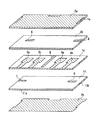
この目的のために、図24に示すような共用器が提案されている(例えば、特許文献1参照)。図24は従来技術における共用器を示す分解斜視図である。 共用 For this purpose, a duplexer as shown in FIG. 24 has been proposed (for example, see Patent Document 1). FIG. 24 is an exploded perspective view showing a duplexer according to the related art.
図24に示すように、誘電体層11pの下面には、第1の端部アース電極(図示せず)が設けられている。また、誘電体層11pには、前記第1の端部アース電極と後述する伝送線路70pの先端部とを接続するためのスルーホール91pが形成されている。
As shown in FIG. 24, a first end ground electrode (not shown) is provided on the lower surface of the dielectric layer 11p. In the dielectric layer 11p, a through-
誘電体層14pの上面には、その一端がそれぞれ前記第1の端部アース電極に接続されて1/4波長型ストリップ線路共振器を構成する共振素子21p、22p、23p、24p、25pが設けられている。また、誘電体層14pの上面には、その一端がそれぞれ前記第1の端部アース電極に接続され、かつ、その他端がそれぞれ共振素子21p、22p、23p、24p、25pの開放端と所定の間隔をもって対向する電極31p、32p、33p、34p、35pが設けられている。そして、共振素子21p、22pが分布結合されることを利用してコムライン形のフィルタ500pが構成され、共振素子23p、24p、25pが分布結合されることを利用してコムライン形のフィルタ600pが構成されている。また、誘電体層14pの上面には、共振素子22pと共振素子23pとの間にインダクタを構成するための伝送線路70pが設けられている。伝送線路70pの先端部には、前記第1の端部アース電極と接続するためのスルーホール94pが形成されている。
誘電体層12pの上面には、共振素子21p、22pの開放端側に位置して前記第1の端部アース電極と接続される内層アース電極81pが設けられており、内層アース電極81pと共振素子21p、22pの開放端側との間には誘電体層13p、14pが介在されている。また、誘電体層12pの上面には、共振素子23p、24p、25pの開放端側に位置して前記第1の端部アース電極と接続される内層アース電極83pが設けられており、内層アース電極83pと共振素子23p、24p、25pの開放端側との間には誘電体層13p、14pが介在されている。また、誘電体層12pには、前記第1の端部アース電極と伝送線路70pの先端部とを接続するためのスルーホール92pが形成されている。
On the upper surface of the
誘電体層13pの上面には、その一端部51pが伝送線路70pの一部に誘電体層14pを挟んで重なり、かつ、その他端部52pが共振素子23pの一部に誘電体層14pを挟んで重なる容量結合電極50pと、共振素子25pの一部に誘電体層14pを挟んで重なる入出力電極42pとが設けられている。また、誘電体層13pには、前記第1の端部アース電極と伝送線路70pの先端部とを接続するためのスルーホール93pが形成されている。
On the upper surface of the
伝送線路70pの先端部は、スルーホール94p、93p、92p、91pを介して誘電体層11pの下面に設けられた前記第1の端部アース電極に短絡される。スルーホール94pは、伝送線路70pの電気長が90度以下の所定の長さとなるような位置に設けられている。このため、伝送線路70pはインダクタを構成する。
先端 A tip of the
誘電体層15pの上面には、その一端部61pが伝送線路70pの一部に誘電体層15pを挟んで重なり、かつ、その他端部62pが共振素子22pの一部に誘電体層15pを挟んで重なる容量電極60pが設けられている。また、誘電体層15pの上面には、その一部が共振素子21pの一部に誘電体層15pを挟んで重なる入出力電極41pが設けられている。
On the upper surface of the
誘電体層17pの上面には、第2の端部アース電極110pが設けられている。
A second
誘電体層16pの上面には、共振素子21p、22pの開放端側に位置して第2の端部アース電極110pと接続される内層アース電極82pが設けられており、内層アース電極82pと共振素子21p、22pの開放端側との間には誘電体層15p、16pが介在されている。また、誘電体層16pの上面には、共振素子23p、24p、25pの開放端側に位置して第2の端部アース電極110pと接続される内層アース電極84pが設けられており、内層アース電極84pと共振素子23p、24p、25pの開放端側との間には誘電体層15p、16pが介在されている。
On the upper surface of the
以上のような構成を有する誘電体層11p、12p、13p、14p、15p、16p、17pを積層して一体化した後、焼成することにより、誘電体層と電極層が交互に積層された積層体からなる共用器が得られる。
After laminating and integrating the
図25に、上記のような構成を有する共用器の等価回路を示す。図24、図25に示すように、共振素子21p、22pによってバンドパスフィルタ500pが構成され、共振素子23p、24p、25pによってバンドパスフィルタ600pが構成されている。静電容量401pは、容量電極60pと伝送線路70pとの間に形成される静電容量であり、静電容量402pは、容量電極50pと伝送線路70pとの間に形成される静電容量である。インダクタ403pは、伝送線路70pによって構成されるインダクタである。インダクタ403pは、フィルタ500p、600pと並列に接続され、静電容量401pは、アンテナ700pとフィルタ500pとの間に直列に接続され、静電容量402pは、アンテナ700pとフィルタ600pとの間に直列に接続されている。これらのインダクタ403p、静電容量401p、402pによって分波回路400pが構成されている。
FIG. 25 shows an equivalent circuit of a duplexer having the above configuration. As shown in FIGS. 24 and 25, a band-
図26に、上記のような構成を有する共用器の伝達特性を示す。図26に示すように、分波回路400pは、1つのアンテナを送信側と受信側とで共用し、送信信号と受信信号とを分離する機能を有することが分かる。
以上のように、従来技術における共用器は、共振素子が誘電体基板中に一体的に設けられて構成されたトリプレート形の2つのフィルタ間に設けられた分波回路を具備している。そして、分波回路は、2つのフィルタにそれぞれ直列に接続された静電容量と、並列に接続されたインダクタとを用いて構成されている。 As described above, the duplexer in the related art includes the branching circuit provided between the two triplate-type filters in which the resonance element is provided integrally in the dielectric substrate. The branching circuit is configured by using a capacitance connected in series to the two filters and an inductor connected in parallel.
しかし、上記した構造では、回路構成が複雑となるために、分波回路での損失が増加すると共に、配置スペースが必然的に大きくなるという問題点があった。また、2つのフィルタにそれぞれ並列に接続されているインダクタは、大きなL値を得ることが困難であるため、設計の自由度が狭くなるという問題点があった。 However, the above-described structure has a problem that the circuit configuration is complicated, so that the loss in the branching circuit increases and the arrangement space is inevitably increased. In addition, since it is difficult to obtain a large L value for the inductors connected in parallel to the two filters, there is a problem that the degree of freedom in design is reduced.
本発明は、従来技術における前記課題を解決するためになされたものであり、非常に簡単な構造によって実現することができ、大幅な低損失化が可能で、容易に小型化を図ることのできる共用器、並びにそれを用いた積層型高周波デバイス及び通信機器を提供することを目的とする。また、本発明は、設計の自由度を十分にとることができるように改良された共用器、並びにそれを用いた積層型高周波デバイス及び通信機器を提供することを目的とする。 The present invention has been made to solve the above-mentioned problems in the prior art, can be realized by a very simple structure, can achieve a significant reduction in loss, can be easily reduced in size. An object of the present invention is to provide a duplexer, and a laminated high-frequency device and a communication device using the same. Another object of the present invention is to provide a duplexer improved so that the degree of freedom of design can be sufficiently obtained, and a stacked high-frequency device and a communication apparatus using the duplexer.
前記目的を達成するため、本発明に係る共用器の第1の構成は、誘電体層と電極層が交互に積層された積層体からなる共用器であって、
前記積層体内に設けられ、互いに通過帯域周波数の異なる、送信用の第1のフィルタと受信用の第2のフィルタと、
前記第1のフィルタと前記第2のフィルタとの間に設けられ、一端が短絡し、他端が外部端子に接続された結合線路からなる整合回路とを備え、
前記第1のフィルタは、一端が短絡した第1ストリップ線路共振器を少なくとも1つ含み、
前記第2のフィルタは、一端が短絡した第2ストリップ線路共振器を少なくとも1つ含み、
前記第1ストリップ線路共振器と前記第2ストリップ線路共振器は、それぞれ前記結合線路と電磁界結合によって結合されていることを特徴とする。
In order to achieve the above object, a first configuration of a duplexer according to the present invention is a duplexer including a laminate in which dielectric layers and electrode layers are alternately laminated,
A first filter for transmission and a second filter for reception provided in the laminate and having different passband frequencies from each other;
A matching circuit provided between the first filter and the second filter, the one end being short-circuited, and the other end including a coupling line connected to an external terminal;
The first filter includes at least one first stripline resonator having one end short-circuited,
The second filter includes at least one second stripline resonator having one end short-circuited,
The first stripline resonator and the second stripline resonator are coupled to the coupling line by electromagnetic field coupling, respectively.
この共用器の第1の構成によれば、インダクタやコンデンサなどの集中定数素子を用いることなく、第1ストリップ線路共振器と第2ストリップ線路共振器のそれぞれを結合線路と電磁界結合によって結合する、という簡単な構造により、共用器を実現することができるので、大幅な低損失化が可能となる。 According to the first configuration of the duplexer, each of the first stripline resonator and the second stripline resonator is coupled to the coupling line and the electromagnetic field without using a lumped element such as an inductor or a capacitor. , A duplexer can be realized, so that the loss can be significantly reduced.
前記本発明の共用器の第1の構成においては、前記第1ストリップ線路共振器と前記第2ストリップ線路共振器の少なくとも一方は、開放端側で広く、短絡端側で狭い線路幅を有するのが好ましい。この好ましい例によれば、第1及び第2ストリップ線路共振器と結合線路との結合度を、それぞれ任意に変化させることが可能となるので、設計の自由度が大幅に向上する。 In the first configuration of the duplexer of the present invention, at least one of the first stripline resonator and the second stripline resonator has a wide line width at an open end side and a narrow line width at a short-circuit end side. Is preferred. According to this preferred example, the degree of coupling between the first and second stripline resonators and the coupling line can be arbitrarily changed, so that the degree of freedom in design is greatly improved.
前記本発明の共用器の第1の構成においては、前記積層体は、順次積層された、第1誘電体層と、第2誘電体層と、第3誘電体層と、第4誘電体層とを含み、
前記電極層は、
前記第1誘電体層の上面に配置された第1シールド電極と、
前記第1誘電体層と前記第2誘電体層との間に配置された、前記第1のフィルタを構成する段間結合容量電極と、前記第2のフィルタを構成する入出力結合容量電極と、
前記第2誘電体層と前記第3誘電体層との間に配置された、前記第1のフィルタを構成する第1共振器電極と、前記第2のフィルタを構成する第2共振器電極と、前記整合回路を構成する結合線路電極と、
前記第3誘電体層と前記第4誘電体層との間に配置された、前記第1のフィルタを構成する入出力結合容量電極と、前記第2のフィルタを構成する段間結合容量電極と、
前記第4誘電体層の下面に配置された第2シールド電極と、
前記第1誘電体層、第2誘電体層、第3誘電体層及び第4誘電体層の側面に設けられ、前記第1のフィルタを構成する前記入出力結合容量電極と前記第2のフィルタを構成する前記入出力結合容量電極と前記結合線路電極のそれぞれに接続された少なくとも3つの端子電極と、
前記第1シールド電極と前記第2シールド電極とを接続する端面電極とを含むのが好ましい。
In the first configuration of the duplexer according to the present invention, the laminated body includes a first dielectric layer, a second dielectric layer, a third dielectric layer, and a fourth dielectric layer which are sequentially laminated. And
The electrode layer,
A first shield electrode disposed on an upper surface of the first dielectric layer;
An inter-stage coupling capacitance electrode configuring the first filter, disposed between the first dielectric layer and the second dielectric layer; and an input / output coupling capacitance electrode configuring the second filter. ,
A first resonator electrode forming the first filter and a second resonator electrode forming the second filter, disposed between the second dielectric layer and the third dielectric layer; A coupling line electrode constituting the matching circuit;
An input / output coupling capacitance electrode constituting the first filter, an inter-stage coupling capacitance electrode constituting the second filter, disposed between the third dielectric layer and the fourth dielectric layer; ,
A second shield electrode disposed on a lower surface of the fourth dielectric layer;
The input / output coupling capacitance electrode provided on a side surface of the first dielectric layer, the second dielectric layer, the third dielectric layer, and the fourth dielectric layer, and constituting the first filter; and the second filter At least three terminal electrodes connected to the input / output coupling capacitance electrode and the coupling line electrode, respectively.
It is preferable to include an end face electrode connecting the first shield electrode and the second shield electrode.
この好ましい例によれば、非常に簡単な構造によって共用器を実現することができるので、大幅な低損失化と小型化が可能となる。 According to this preferred example, since the duplexer can be realized with a very simple structure, it is possible to greatly reduce the loss and reduce the size.
また、この場合には、前記第1誘電体層、第2誘電体層、第3誘電体層及び第4誘電体層の少なくとも一層は、他の誘電体層と異なる誘電率を有するのが好ましい。この好ましい例によれば、コンデンサの容量を調節することができる。 In this case, it is preferable that at least one of the first, second, third, and fourth dielectric layers has a different dielectric constant from the other dielectric layers. . According to this preferred example, the capacity of the capacitor can be adjusted.
また、この場合には、前記第1誘電体層を間に挟んで、前記第1シールド電極と対向させて設けられた調整用容量電極をさらに備えているのが好ましい。アンテナは、送信と受信の双方に用いられるが、この好ましい例によれば、送信と受信の整合を最適化することができる。 In this case, it is preferable to further include an adjusting capacitor electrode provided so as to face the first shield electrode with the first dielectric layer interposed therebetween. The antenna is used for both transmission and reception, but according to this preferred example, transmission and reception matching can be optimized.
前記本発明の共用器の第1の構成においては、前記第1ストリップ線路共振器と前記第2ストリップ線路共振器の少なくとも一方は、前記結合線路が形成された誘電体層とは異なる誘電体層に形成されているのが好ましい。この好ましい例によれば、設計の自由度、融通性を持たせることができる。 In the first configuration of the duplexer of the present invention, at least one of the first stripline resonator and the second stripline resonator is a dielectric layer different from the dielectric layer on which the coupling line is formed. Is preferably formed. According to this preferred example, design flexibility and flexibility can be provided.
前記本発明の共用器の第1の構成においては、前記結合線路は、互いに連結された、線路幅の異なる少なくとも2つのストリップ線路からなるのが好ましい。この好ましい例によれば、電磁界結合の強さを任意に変更することができる。 In the first configuration of the duplexer of the present invention, it is preferable that the coupling line includes at least two strip lines connected to each other and having different line widths. According to this preferred example, the strength of the electromagnetic field coupling can be arbitrarily changed.
前記本発明の共用器の第1の構成においては、前記結合線路が複数本のストリップ線路からなり、前記複数本のストリップ線路は、それぞれ異なる誘電体層に設けられているのが好ましい。この好ましい例によれば、電位の安定化を図ることができる。また、この場合には、前記複数本のストリップ線路のうち少なくとも1つは、他のストリップ線路と異なる線路幅を有するのが好ましい。この好ましい例によれば、より強い電磁界結合を得ることが可能となる。また、この場合には、前記複数本のストリップ線路が、ビアホールによって互いに接続されているのが好ましい。この好ましい例によれば、ビアホールのシールド効果により、第1ストリップ線路共振器と第2ストリップ線路共振器を分離することができるので、送信時に、受信側へ周波数成分が行くのを防止し、受信時に、送信側へ周波数成分が行くのを防止することができる。 In the first configuration of the duplexer of the present invention, it is preferable that the coupling line includes a plurality of strip lines, and the plurality of strip lines are provided on different dielectric layers. According to this preferred example, the potential can be stabilized. In this case, it is preferable that at least one of the plurality of strip lines has a line width different from that of the other strip lines. According to this preferred example, it is possible to obtain stronger electromagnetic field coupling. In this case, it is preferable that the plurality of strip lines are connected to each other by a via hole. According to this preferred example, the first strip line resonator and the second strip line resonator can be separated by the shield effect of the via hole, so that the frequency component is prevented from going to the receiving side during transmission, and the reception is prevented. Sometimes, it is possible to prevent the frequency component from going to the transmitting side.
前記本発明の共用器の第1の構成においては、誘電体層を介在させて前記結合線路及び前記ストリップ線路共振器と重なるように設けられた結合コンデンサをさらに備えているのが好ましい。この好ましい例によれば、結合コンデンサによって生じる電界結合と、ストリップ線路共振器と結合線路との間に生じる電磁界結合とが組み合わされる。ストリップ線路共振器と結合線路との間に生じる結合は、磁界成分が支配的であるが、結合コンデンサを設けることにより、電界容量成分を増やすことができる。 In the first configuration of the duplexer according to the present invention, it is preferable that the duplexer further includes a coupling capacitor provided so as to overlap the coupling line and the strip line resonator with a dielectric layer interposed therebetween. According to this preferred example, the electric field coupling generated by the coupling capacitor and the electromagnetic field coupling generated between the stripline resonator and the coupling line are combined. The magnetic field component is dominant in the coupling between the stripline resonator and the coupling line, but the electric field capacitance component can be increased by providing the coupling capacitor.
前記本発明の共用器の第1の構成においては、前記第1のフィルタと前記第2のフィルタは、シールド電極を介在させて対向して設けられているのが好ましい。この好ましい例によれば、送信用の第1のフィルタと受信用の第2のフィルタを縦方向に並べることができるので、共用器の占有面積を小さくすることができる。 In the first configuration of the duplexer of the present invention, it is preferable that the first filter and the second filter are provided to face each other with a shield electrode interposed therebetween. According to this preferred example, the first filter for transmission and the second filter for reception can be arranged in the vertical direction, so that the area occupied by the duplexer can be reduced.
また、この場合には、前記積層体は、順次積層された、第1誘電体層と、第2誘電体層と、第3誘電体層と、第4誘電体層と、第5誘電体層と、第6誘電体層とを含み、
前記電極層は、
前記第1誘電体層の上面に配置された第1シールド電極と、
前記第1誘電体層と前記第2誘電体層との間に配置された、前記第1のフィルタを構成する、段間結合容量電極及び入出力結合容量電極と、
前記第2誘電体層と前記第3誘電体層との間に配置された、前記第1のフィルタを構成する複数個の共振器電極と、
前記第3誘電体層と前記第4誘電体層との間に配置された、第3のシールド電極と、前記整合回路を構成する結合線路電極と、
前記第4誘電体層と前記第5誘電体層との間に配置された、前記第2のフィルタを構成する、複数個の共振器電極及び当該共振器電極に接続された入出力線路電極と、
前記第5誘電体層と前記第6誘電体層との間に配置された、前記第2のフィルタを構成する段間結合容量電極と、
前記第6誘電体層の下面に配置された第2シールド電極と、
前記第1誘電体層、第2誘電体層、第3誘電体層、第4誘電体層、第5誘電体層及び第6誘電体層の側面に設けられ、前記入出力結合容量電極と前記入出力線路電極と前記結合線路電極のそれぞれに接続された少なくとも3つの端子電極と、
前記第1シールド電極と前記第2シールド電極と前記第3シールド電極とを接続する端面電極とを含むのが好ましい。
Further, in this case, the laminate includes a first dielectric layer, a second dielectric layer, a third dielectric layer, a fourth dielectric layer, and a fifth dielectric layer which are sequentially laminated. And a sixth dielectric layer,
The electrode layer,
A first shield electrode disposed on an upper surface of the first dielectric layer;
An interstage coupling capacitance electrode and an input / output coupling capacitance electrode, which constitute the first filter, are disposed between the first dielectric layer and the second dielectric layer;
A plurality of resonator electrodes constituting the first filter, disposed between the second dielectric layer and the third dielectric layer;
A third shield electrode disposed between the third dielectric layer and the fourth dielectric layer, and a coupling line electrode forming the matching circuit;
A plurality of resonator electrodes and an input / output line electrode connected to the resonator electrodes, which are arranged between the fourth dielectric layer and the fifth dielectric layer, and constitute the second filter; ,
An inter-stage coupling capacitance electrode constituting the second filter, disposed between the fifth dielectric layer and the sixth dielectric layer;
A second shield electrode disposed on a lower surface of the sixth dielectric layer;
A first dielectric layer, a second dielectric layer, a third dielectric layer, a fourth dielectric layer, a fifth dielectric layer, and a sixth dielectric layer. At least three terminal electrodes connected to each of the writing output line electrode and the coupling line electrode;
It is preferable to include an end face electrode connecting the first shield electrode, the second shield electrode, and the third shield electrode.
この好ましい例によれば、第1のフィルタと第2のフィルタを縦方向に並べることができるので、共用器の占有面積を小さくすることができる。 According to this preferred example, since the first filter and the second filter can be arranged in the vertical direction, the area occupied by the duplexer can be reduced.
本発明に係る共用器の第2の構成は、誘電体層と電極層が交互に積層された積層体からなる共用器であって、
前記積層体内に積層方向に並んで配置された第1シールド電極、第2シールド電極、第3シールド電極及び第4シールド電極と、
前記第1シールド電極と第2シールド電極との間に配置され、一端が短絡したストリップ線路共振器が複数個平行に近接して構成された第1のフィルタと、
前記第2シールド電極と第3シールド電極との間に配置され、結合線路からなる整合回路と、
前記第3シールド電極と前記第4シールド電極との間に配置され、一端が短絡したストリップ線路共振器が複数個平行に近接して構成され、前記第1のフィルタと通過帯域周波数の異なる第2のフィルタとを備え、
前記第2及び第3シールド電極には結合窓が設けられ、
前記第1及び第2のフィルタを構成する前記ストリップ線路共振器と前記結合線路とが、それぞれ前記結合窓を介して、電磁界結合によって結合されていることを特徴とする。
A second configuration of the duplexer according to the present invention is a duplexer including a laminate in which dielectric layers and electrode layers are alternately laminated,
A first shield electrode, a second shield electrode, a third shield electrode, and a fourth shield electrode arranged in the stack in the stacking direction;
A first filter disposed between the first shield electrode and the second shield electrode, wherein a plurality of stripline resonators having one end short-circuited are arranged in parallel and close to each other;
A matching circuit disposed between the second shield electrode and the third shield electrode, the matching circuit including a coupling line;
A plurality of strip line resonators each of which is disposed between the third shield electrode and the fourth shield electrode, and one end of which is short-circuited, are configured in parallel and close to each other, and have a second pass band frequency different from that of the first filter. With a filter of
A coupling window is provided in the second and third shield electrodes,
The strip line resonator and the coupling line that constitute the first and second filters are coupled by electromagnetic coupling through the coupling window.
この共用器の第2の構成によれば、電磁界結合の強さの融通性を、簡単に図ることができる。 According to the second configuration of the duplexer, flexibility in the strength of electromagnetic field coupling can be easily achieved.
前記本発明の共用器の第2の構成においては、前記積層体は、順次積層された、第1誘電体層と、第2誘電体層と、第3誘電体層と、第4誘電体層と、第5誘電体層と、第6誘電体層と、第7誘電体層と、第8誘電体層とを含み、
前記電極層は、
前記第1誘電体層の上面に配置された第1シールド電極と、
前記第1誘電体層と前記第2誘電体層との間に配置された、前記第1のフィルタを構成する、段間結合容量電極及び入出力結合容量電極と、
前記第2誘電体層と前記第3誘電体層との間に配置された、前記第1のフィルタを構成する複数個の共振器電極と、
前記第3誘電体層と前記第4誘電体層との間に配置され、一部に前記結合窓が設けられた第3のシールド電極と、
前記第4誘電体層と前記第5誘電体層との間に配置された、前記整合回路を構成する結合線路電極と、
前記第5誘電体層と前記第6誘電体層との間に配置され、一部に前記結合窓が設けられた第4シールド電極と、
前記第6誘電体層と前記第7誘電体層との間に配置され、前記第2のフィルタを構成する、複数個の共振器電極及び当該共振器電極に接続された入出力線路電極と、
前記第7誘電体層と前記第8誘電体層との間に配置された、前記第2のフィルタを構成する段間結合容量電極と、
前記第8の誘電体層の下面に配置された第2のシールド電極と、
前記第1誘電体層、第2誘電体層、第3誘電体層、第4誘電体層、第5誘電体層、第6誘電体層、第7誘電体層及び第8誘電体層の側面に設けられ、前記入出力結合容量電極と前記入出力線路電極と前記結合線路電極のそれぞれに接続された少なくとも3つの端子電極と、
前記第1シールド電極と前記第2シールド電極と前記第3シールド電極と前記第4シールド電極とを接続する端面電極とを含んでいるのが好ましい。
In the second configuration of the duplexer according to the present invention, the stacked body may include a first dielectric layer, a second dielectric layer, a third dielectric layer, and a fourth dielectric layer that are sequentially stacked. And a fifth dielectric layer, a sixth dielectric layer, a seventh dielectric layer, and an eighth dielectric layer,
The electrode layer,
A first shield electrode disposed on an upper surface of the first dielectric layer;
An interstage coupling capacitance electrode and an input / output coupling capacitance electrode, which constitute the first filter, are disposed between the first dielectric layer and the second dielectric layer;
A plurality of resonator electrodes constituting the first filter, disposed between the second dielectric layer and the third dielectric layer;
A third shield electrode disposed between the third dielectric layer and the fourth dielectric layer and partially provided with the coupling window;
A coupling line electrode that is arranged between the fourth dielectric layer and the fifth dielectric layer and that constitutes the matching circuit;
A fourth shield electrode disposed between the fifth dielectric layer and the sixth dielectric layer and partially provided with the coupling window;
A plurality of resonator electrodes disposed between the sixth dielectric layer and the seventh dielectric layer and constituting the second filter, and input / output line electrodes connected to the resonator electrodes;
An inter-stage coupling capacitance electrode constituting the second filter, disposed between the seventh dielectric layer and the eighth dielectric layer;
A second shield electrode disposed on a lower surface of the eighth dielectric layer;
Side faces of the first, second, third, fourth, fifth, sixth, seventh, and eighth dielectric layers And at least three terminal electrodes respectively connected to the input / output coupling capacitance electrode, the input / output line electrode, and the coupling line electrode;
It is preferable to include an end face electrode for connecting the first shield electrode, the second shield electrode, the third shield electrode, and the fourth shield electrode.
この好ましい例によれば、誘電体層の上にシールド電極を印刷するときに、その一部を印刷せずに結合窓を設ける、という簡単な方法により、電磁界結合の強さを容易に変えることができる。 According to this preferred example, when the shield electrode is printed on the dielectric layer, the strength of the electromagnetic field coupling is easily changed by a simple method of providing a coupling window without printing a part thereof. be able to.
本発明に係る共用器の第3の構成は、誘電体層と電極層が交互に積層された積層体からなる共用器であって、
前記積層体内に設けられ、互いに通過帯域周波数の異なる、送信用の第1のフィルタと受信用の第2のフィルタと、
前記第1のフィルタと前記第2のフィルタとの間に設けられ、一端が開放し、他端が外部端子に接続された結合線路からなる整合回路とを備え、
前記第1のフィルタは、一端が短絡した第1ストリップ線路共振器を少なくとも1つ含み、
前記第2のフィルタは、一端が短絡した第2ストリップ線路共振器を少なくとも1つ含み、
前記第1ストリップ線路共振器と前記第2ストリップ線路共振器は、それぞれ前記結合線路と電磁界結合によって結合されていることを特徴とする。
A third configuration of the duplexer according to the present invention is a duplexer including a laminate in which dielectric layers and electrode layers are alternately laminated,
A first filter for transmission and a second filter for reception provided in the laminate and having different passband frequencies from each other;
A matching circuit provided between the first filter and the second filter, the matching circuit including a coupling line having one end open and the other end connected to an external terminal;
The first filter includes at least one first stripline resonator having one end short-circuited,
The second filter includes at least one second stripline resonator having one end short-circuited,
The first stripline resonator and the second stripline resonator are coupled to the coupling line by electromagnetic field coupling, respectively.
この共用器の第3の構成によれば、一端が開放し、他端が外部端子に接続された結合線路を用いることによっても、共用器として動作させることができる。 According to the third configuration of the duplexer, it is possible to operate as a duplexer by using a coupling line having one end open and the other end connected to an external terminal.
前記本発明の共用器の第3の構成においては、前記結合線路の開放端側に、誘電体層を介在させて整合用容量電極が接続されているのが好ましい。結合線路9一端を開放した場合には、開放端に浮遊容量が生じ、ばらつきの要因となるが、この好ましい例によれば、安定化させることができる。また、容量値を変えることにより、設計の自由度を得ることができる。
In the third configuration of the duplexer of the present invention, it is preferable that a matching capacitance electrode is connected to the open end side of the coupling line via a dielectric layer. When one end of the
前記本発明の共用器の第3の構成においては、前記第1ストリップ線路共振器と前記第2ストリップ線路共振器の少なくとも一方は、開放端側で広く、短絡端側で狭い線路幅を有するのが好ましい。 In the third configuration of the duplexer of the present invention, at least one of the first stripline resonator and the second stripline resonator has a wide line width at an open end and a narrow line width at a short end. Is preferred.
前記本発明の共用器の第3の構成においては、前記積層体は、順次積層された、第1誘電体層と、第2誘電体層と、第3誘電体層と、第4誘電体層とを含み、
前記電極層は、
前記第1誘電体層の上面に配置された第1シールド電極と、
前記第1誘電体層と前記第2誘電体層との間に配置された、前記第1のフィルタを構成する段間結合容量電極と、前記第2のフィルタを構成する入出力結合容量電極と、
前記第2誘電体層と前記第3誘電体層との間に配置された、前記第1のフィルタを構成する第1共振器電極と、前記第2のフィルタを構成する第2共振器電極と、前記整合回路を構成する結合線路電極と、
前記第3誘電体層と前記第4誘電体層との間に配置された、前記第1のフィルタを構成する入出力結合容量電極と、前記第2のフィルタを構成する段間結合容量電極と、
前記第4誘電体層の下面に配置された第2シールド電極と、
前記第1誘電体層、第2誘電体層、第3誘電体層及び第4誘電体層の側面に設けられ、前記第1のフィルタを構成する前記入出力結合容量電極と前記第2のフィルタを構成する前記入出力結合容量電極と前記結合線路電極のそれぞれに接続された少なくとも3つの端子電極と、
前記第1シールド電極と前記第2シールド電極とを接続する端面電極とを含むのが好ましい。
In the third configuration of the duplexer according to the present invention, the laminate may include a first dielectric layer, a second dielectric layer, a third dielectric layer, and a fourth dielectric layer that are sequentially laminated. And
The electrode layer,
A first shield electrode disposed on an upper surface of the first dielectric layer;
An inter-stage coupling capacitance electrode configuring the first filter, disposed between the first dielectric layer and the second dielectric layer; and an input / output coupling capacitance electrode configuring the second filter. ,
A first resonator electrode forming the first filter and a second resonator electrode forming the second filter, disposed between the second dielectric layer and the third dielectric layer; A coupling line electrode constituting the matching circuit;
An input / output coupling capacitance electrode constituting the first filter, an inter-stage coupling capacitance electrode constituting the second filter, disposed between the third dielectric layer and the fourth dielectric layer; ,
A second shield electrode disposed on a lower surface of the fourth dielectric layer;
The input / output coupling capacitance electrode provided on a side surface of the first dielectric layer, the second dielectric layer, the third dielectric layer, and the fourth dielectric layer, and constituting the first filter; and the second filter At least three terminal electrodes connected to the input / output coupling capacitance electrode and the coupling line electrode, respectively.
It is preferable to include an end face electrode connecting the first shield electrode and the second shield electrode.
また、この場合には、前記第1誘電体層、第2誘電体層、第3誘電体層及び第4誘電体層の少なくとも一層は、他の誘電体層と異なる誘電率を有するのが好ましい。 In this case, it is preferable that at least one of the first, second, third, and fourth dielectric layers has a different dielectric constant from the other dielectric layers. .
また、この場合には、前記第1誘電体層を間に挟んで、前記第1シールド電極と対向させて設けられた調整用容量電極をさらに備えているのが好ましい。 In this case, it is preferable to further include an adjusting capacitor electrode provided so as to face the first shield electrode with the first dielectric layer interposed therebetween.
前記本発明の共用器の第3の構成においては、前記第1ストリップ線路共振器と前記第2ストリップ線路共振器の少なくとも一方は、前記結合線路が形成された誘電体層とは異なる誘電体層に形成されているのが好ましい。 In the third configuration of the duplexer according to the present invention, at least one of the first stripline resonator and the second stripline resonator is a dielectric layer different from the dielectric layer on which the coupling line is formed. Is preferably formed.
前記本発明の共用器の第3の構成においては、前記結合線路は、互いに連結された、線路幅の異なる少なくとも2つのストリップ線路からなるのが好ましい。 In the third configuration of the duplexer of the present invention, it is preferable that the coupling line includes at least two strip lines connected to each other and having different line widths.
前記本発明の共用器の第3の構成においては、前記結合線路が複数本のストリップ線路からなり、前記複数本のストリップ線路は、それぞれ異なる誘電体層に設けられているのが好ましい。また、この場合には、前記複数本のストリップ線路のうち少なくとも1つは、他のストリップ線路と異なる線路幅を有するのが好ましい。また、この場合には、前記複数本のストリップ線路が、ビアホールによって互いに接続されているのが好ましい。 In the third configuration of the duplexer according to the present invention, it is preferable that the coupling line includes a plurality of strip lines, and the plurality of strip lines are provided on different dielectric layers. In this case, it is preferable that at least one of the plurality of strip lines has a line width different from that of the other strip lines. In this case, it is preferable that the plurality of strip lines are connected to each other by a via hole.
前記本発明の共用器の第3の構成においては、誘電体層を介在させて前記結合線路及び前記ストリップ線路共振器と重なるように設けられた結合コンデンサをさらに備えているのが好ましい。 In the third configuration of the duplexer of the present invention, it is preferable that the duplexer further includes a coupling capacitor provided so as to overlap the coupling line and the strip line resonator with a dielectric layer interposed therebetween.
前記本発明の共用器の第3の構成においては、前記第1のフィルタと前記第2のフィルタは、シールド電極を介在させて対向して設けられているのが好ましい。 In the third configuration of the duplexer of the present invention, it is preferable that the first filter and the second filter are provided to face each other with a shield electrode interposed therebetween.
また、この場合には、前記積層体は、順次積層された、第1誘電体層と、第2誘電体層と、第3誘電体層と、第4誘電体層と、第5誘電体層と、第6誘電体層とを含み、
前記電極層は、
前記第1誘電体層の上面に配置された第1シールド電極と、
前記第1誘電体層と前記第2誘電体層との間に配置された、前記第1のフィルタを構成する、段間結合容量電極及び入出力結合容量電極と、
前記第2誘電体層と前記第3誘電体層との間に配置された、前記第1のフィルタを構成する複数個の共振器電極と、
前記第3誘電体層と前記第4誘電体層との間に配置された、第3のシールド電極と、前記整合回路を構成する結合線路電極と、
前記第4誘電体層と前記第5誘電体層との間に配置された、前記第2のフィルタを構成する、複数個の共振器電極及び当該共振器電極に接続された入出力線路電極と、
前記第5誘電体層と前記第6誘電体層との間に配置された、前記第2のフィルタを構成する段間結合容量電極と、
前記第6誘電体層の下面に配置された第2シールド電極と、
前記第1誘電体層、第2誘電体層、第3誘電体層、第4誘電体層、第5誘電体層及び第6誘電体層の側面に設けられ、前記入出力結合容量電極と前記入出力線路電極と前記結合線路電極のそれぞれに接続された少なくとも3つの端子電極と、
前記第1シールド電極と前記第2シールド電極と前記第3シールド電極とを接続する端面電極とを含むのが好ましい。
Further, in this case, the laminate includes a first dielectric layer, a second dielectric layer, a third dielectric layer, a fourth dielectric layer, and a fifth dielectric layer which are sequentially laminated. And a sixth dielectric layer,
The electrode layer,
A first shield electrode disposed on an upper surface of the first dielectric layer;
An interstage coupling capacitance electrode and an input / output coupling capacitance electrode, which constitute the first filter, are disposed between the first dielectric layer and the second dielectric layer;
A plurality of resonator electrodes constituting the first filter, disposed between the second dielectric layer and the third dielectric layer;
A third shield electrode disposed between the third dielectric layer and the fourth dielectric layer, and a coupling line electrode forming the matching circuit;
A plurality of resonator electrodes and an input / output line electrode connected to the resonator electrodes, which are arranged between the fourth dielectric layer and the fifth dielectric layer, and constitute the second filter; ,
An inter-stage coupling capacitance electrode constituting the second filter, disposed between the fifth dielectric layer and the sixth dielectric layer;
A second shield electrode disposed on a lower surface of the sixth dielectric layer;
A first dielectric layer, a second dielectric layer, a third dielectric layer, a fourth dielectric layer, a fifth dielectric layer, and a sixth dielectric layer. At least three terminal electrodes connected to each of the writing output line electrode and the coupling line electrode;
It is preferable to include an end face electrode connecting the first shield electrode, the second shield electrode, and the third shield electrode.
本発明に係る共用器の第4の構成は、誘電体層と電極層が交互に積層された積層体からなる共用器であって、
前記積層体内に設けられ、互いに通過帯域周波数の異なる、送信用の第1のフィルタと受信用の第2のフィルタと、
前記第1のフィルタと前記第2のフィルタとの間に設けられ、結合線路からなる整合回路とを備え、
前記第1及び第2のフィルタのうちの少なくとも一方は、帯域阻止特性を有する、一端が短絡したストリップ線路共振器と伝送線路とからなるフィルタであり、
前記伝送線路と前記結合線路が電磁界結合によって結合されていることを特徴とする。
A fourth configuration of the duplexer according to the present invention is a duplexer including a laminate in which dielectric layers and electrode layers are alternately laminated,
A first filter for transmission and a second filter for reception provided in the laminate and having different passband frequencies from each other;
A matching circuit provided between the first filter and the second filter, the matching circuit including a coupling line;
At least one of the first and second filters is a filter having a band rejection characteristic and including a transmission line and a strip line resonator having one end short-circuited,
The transmission line and the coupling line are coupled by electromagnetic field coupling.
この共用器の第4の構成によれば、特定の高周波成分のみを阻止するフィルタとなる。帯域阻止特性を有するフィルタは、帯域通過特性を有するフィルタに比べて、低損失化を図ることができるので、送信フィルタの損失を低減することが可能となる。 According to the fourth configuration of the duplexer, a filter that blocks only a specific high-frequency component is provided. The filter having the band rejection characteristic can reduce the loss compared to the filter having the band-pass characteristic, so that the loss of the transmission filter can be reduced.
前記本発明の共用器の第4の構成においては、前記積層体は、順次積層された、第1誘電体層と、第2誘電体層と、第3誘電体層と、第4誘電体層と、第5誘電体層とを含み、
前記電極層は、
前記第1誘電体層の上面に配置された第1シールド電極と、
前記第1誘電体層と前記第2誘電体層との間に配置された、前記第1のフィルタを構成する段間結合容量電極と、
前記第2誘電体層と前記第3誘電体層との間に配置された、前記第1のフィルタを構成する複数個の共振器電極と、前記整合回路を構成する結合線路電極と、
前記第3誘電体層と前記第4誘電体層との間に配置された、前記第1のフィルタを構成する入出力結合容量電極と、帯域阻止特性を有する前記第2フィルタを構成する伝送線路電極と、整合回路を構成する結合線路電極と、
前記第4誘電体層と前記第5誘電体層との間に配置された、前記第2のフィルタを構成する共振器電極と、
前記第5の誘電体層の下面に配置された第2のシールド電極と、
前記第1誘電体層、第2誘電体層、第3誘電体層、第4誘電体層及び第5誘電体層の側面に設けられ、前記入出力結合容量電極と前記伝送線路電極と前記結合線路電極にそれぞれ接続された少なくとも3つの端子電極と、
前記第1シールド電極と第2シールド電極とを接続する端面電極とを含んでいるのが好ましい。
In a fourth configuration of the duplexer according to the present invention, the laminate includes a first dielectric layer, a second dielectric layer, a third dielectric layer, and a fourth dielectric layer that are sequentially laminated. And a fifth dielectric layer,
The electrode layer,
A first shield electrode disposed on an upper surface of the first dielectric layer;
An inter-stage coupling capacitance electrode that constitutes the first filter and is disposed between the first dielectric layer and the second dielectric layer;
A plurality of resonator electrodes constituting the first filter, disposed between the second dielectric layer and the third dielectric layer, and a coupling line electrode constituting the matching circuit;
An input / output coupling capacitance electrode forming the first filter, disposed between the third dielectric layer and the fourth dielectric layer, and a transmission line forming the second filter having band rejection characteristics An electrode, a coupling line electrode forming a matching circuit,
A resonator electrode constituting the second filter, disposed between the fourth dielectric layer and the fifth dielectric layer;
A second shield electrode disposed on a lower surface of the fifth dielectric layer;
The first dielectric layer, the second dielectric layer, the third dielectric layer, the fourth dielectric layer, and the fifth dielectric layer are provided on side surfaces of the first dielectric layer, the second dielectric layer, the fourth dielectric layer, and the fifth dielectric layer. At least three terminal electrodes respectively connected to the line electrode;
It is preferable to include an end face electrode connecting the first shield electrode and the second shield electrode.
この好ましい例によれば、上記のような積層構造とすることにより、帯域阻止特性を有するフィルタを、容易に形成することができる。 According to this preferred example, a filter having band rejection characteristics can be easily formed by adopting the above-described laminated structure.
前記本発明の共用器の第4の構成においては、前記積層体は、順次積層された、第1誘電体層と、第2誘電体層と、第3誘電体層と、第4誘電体層と、第5誘電体層とを含み、
前記電極層は、
前記第1誘電体層の上面に配置された第1シールド電極と、
前記第1誘電体層と前記第2誘電体層との間に配置された、前記第1のフィルタを構成する段間結合容量電極と、
前記第2誘電体層と前記第3誘電体層との間に配置された、前記第1のフィルタを構成する複数個の共振器電極と、前記整合回路を構成する結合線路電極と、
前記第3誘電体層と前記第4誘電体層との間に配置された、前記第1のフィルタを構成する入出力結合容量電極と、帯域阻止特性を有する前記第2フィルタを構成する伝送線路電極と、
前記第4誘電体層と前記第5誘電体層との間に配置された、前記第2のフィルタを構成する共振器電極と、
前記第5の誘電体層の下面に配置された第2のシールド電極と、
前記第1誘電体層、第2誘電体層、第3誘電体層、第4誘電体層及び第5誘電体層の側面に設けられ、前記入出力結合容量電極と前記伝送線路電極と前記結合線路電極にそれぞれ接続された少なくとも3つの端子電極と、
前記第1シールド電極と第2シールド電極とを接続する端面電極とを含み、
前記伝送線路電極の一部分は、積層方向への投影において、前記第3誘電体層を介在させて前記結合線路電極と重なっており、
前記積層方向への投影において、前記伝送線路電極の前記一部分の幅は、前記結合線路電極の幅と同一であるか又は異なっているのが好ましい。
In a fourth configuration of the duplexer according to the present invention, the laminate includes a first dielectric layer, a second dielectric layer, a third dielectric layer, and a fourth dielectric layer that are sequentially laminated. And a fifth dielectric layer,
The electrode layer,
A first shield electrode disposed on an upper surface of the first dielectric layer;
An inter-stage coupling capacitance electrode that constitutes the first filter and is disposed between the first dielectric layer and the second dielectric layer;
A plurality of resonator electrodes constituting the first filter, disposed between the second dielectric layer and the third dielectric layer, and a coupling line electrode constituting the matching circuit;
An input / output coupling capacitance electrode forming the first filter, disposed between the third dielectric layer and the fourth dielectric layer, and a transmission line forming the second filter having band rejection characteristics Electrodes and
A resonator electrode constituting the second filter, disposed between the fourth dielectric layer and the fifth dielectric layer;
A second shield electrode disposed on a lower surface of the fifth dielectric layer;
The first dielectric layer, the second dielectric layer, the third dielectric layer, the fourth dielectric layer, and the fifth dielectric layer are provided on side surfaces of the first dielectric layer, the second dielectric layer, the fourth dielectric layer, and the fifth dielectric layer. At least three terminal electrodes respectively connected to the line electrodes;
An end face electrode for connecting the first shield electrode and the second shield electrode,
A part of the transmission line electrode overlaps with the coupling line electrode with the third dielectric layer interposed therebetween in the projection in the stacking direction,
In the projection in the stacking direction, the width of the portion of the transmission line electrode is preferably the same as or different from the width of the coupling line electrode.
この好ましい例によれば、結合線路電極と伝送線路電極を縦方向に上下に配置しているので、電磁界結合がより強くなる。また、伝送線路電極の一部分の幅を、結合線路電極の幅と異ならせることにより、積層時に重なり合いのずれに対して余裕を持たせることができる。 According to this preferred example, since the coupling line electrode and the transmission line electrode are arranged vertically in the vertical direction, the electromagnetic field coupling becomes stronger. In addition, by making the width of a part of the transmission line electrode different from the width of the coupling line electrode, it is possible to provide a margin for the displacement of the overlap at the time of lamination.
本発明に係る積層型高周波デバイスの構成は、誘電体層と電極層が交互に積層された積層体からなる共用器と、
前記積層体の上面に実装された半導体チップ及び/又は弾性表面波デバイスとを備えた積層型高周波デバイスであって、
前記共用器として前記本発明の共用器を用いたことを特徴とする。
The configuration of the stacked high-frequency device according to the present invention, a duplexer comprising a stacked body in which dielectric layers and electrode layers are alternately stacked,
A laminated high-frequency device including a semiconductor chip and / or surface acoustic wave device mounted on the upper surface of the laminate,
The duplexer of the present invention is used as the duplexer.
この積層型高周波デバイスの構成によれば、共用器を非常に簡単な構造で実現することができるので、大幅な低損失化が可能な、半導体チップ及び/又は弾性表面波デバイスを備えた、積層型高周波デバイスを得ることができる。 According to the configuration of the laminated high-frequency device, the duplexer can be realized with a very simple structure, and therefore, the laminated device including the semiconductor chip and / or the surface acoustic wave device capable of significantly reducing the loss can be realized. Type high frequency device can be obtained.
本発明に係る通信機器の構成は、アンテナと、
送信回路から出た周波数成分を前記アンテナに送り、かつ、前記アンテナから受信した周波数成分を受信回路に送る、誘電体層と電極層が交互に積層された積層体からなる共用器とを備えた通信機器であって、
前記共用器として前記本発明の共用器を用いたことを特徴とする。
The configuration of the communication device according to the present invention, an antenna,
A duplexer comprising a laminated body in which dielectric layers and electrode layers are alternately laminated, wherein a frequency component output from a transmitting circuit is transmitted to the antenna, and a frequency component received from the antenna is transmitted to a receiving circuit. A communication device,
The duplexer of the present invention is used as the duplexer.
この通信機器の構成によれば、共用器を非常に簡単な構造で実現することができるので、大幅な低損失化が可能な通信機器を得ることができる。 According to the configuration of the communication device, since the duplexer can be realized with a very simple structure, it is possible to obtain a communication device capable of greatly reducing loss.
前記本発明の通信機器の構成においては、前記積層体の上面に実装された半導体チップ及び/又は弾性表面波デバイスとをさらに備えているのが好ましい。この好ましい例によれば、大幅な低損失化が可能な、半導体チップ及び/又は弾性表面波デバイスを備えた、積層型高周波デバイスを含む通信機器を得ることができる。 In the configuration of the communication device of the present invention, it is preferable that the communication device further includes a semiconductor chip and / or a surface acoustic wave device mounted on the upper surface of the laminate. According to this preferred example, it is possible to obtain a communication device including a laminated high-frequency device provided with a semiconductor chip and / or a surface acoustic wave device, which can greatly reduce the loss.
本発明によれば、非常に簡単な構造によって実現することができ、大幅な低損失化が可能で、容易に小型化を図ることのできる共用器、並びにそれを用いた積層型高周波デバイス及び通信機器を得ることができる。また、本発明によれば、設計の自由度を十分にとることができるように改良された共用器、並びにそれを用いた積層型高周波デバイス及び通信機器を得ることができる。 According to the present invention, a duplexer that can be realized with a very simple structure, can achieve a significant reduction in loss, and can be easily miniaturized, and a stacked high-frequency device and communication using the same Equipment can be obtained. Further, according to the present invention, it is possible to obtain a duplexer improved so that the degree of freedom of design can be sufficiently obtained, and a laminated high-frequency device and a communication apparatus using the duplexer.
以下、実施の形態を用いて本発明をさらに具体的に説明する。 Hereinafter, the present invention will be described more specifically with reference to embodiments.
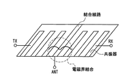
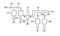
図1は本発明の実施の形態における共用器を示す概念図である。図1に示すように、本実施の形態の共用器においては、共振器と結合線路が、誘電体基板中に一体的に設けられている。送信、受信用の2つのフィルタは、トリプレート形に構成されている。送信フィルタと受信フィルタとの間には、結合線路からなる整合回路が設けられている。結合線路は、アンテナ端子(ANT)に接続されている。送信フィルタは、送信回路の端子(TX)に接続され、受信フィルタは、受信回路の端子(RX)に接続されている。送信フィルタ及び受信フィルタの、結合線路に最も近い共振器と、結合線路とは、直接、電磁界結合(M)によって結合されている。すなわち、送受各フィルタの共振器と結合線路を、磁界結合と電界結合の組み合わせによって高周波的に結合することにより、所望の共用器特性が実現されている。このように、本実施の形態によれば、非常に簡単な構造によって共用器を実現することができるので、大幅な低損失化が可能となる。 FIG. 1 is a conceptual diagram showing a duplexer according to an embodiment of the present invention. As shown in FIG. 1, in the duplexer of the present embodiment, a resonator and a coupling line are provided integrally in a dielectric substrate. The two filters for transmission and reception are configured in a triplate shape. A matching circuit including a coupling line is provided between the transmission filter and the reception filter. The coupling line is connected to an antenna terminal (ANT). The transmission filter is connected to a terminal (TX) of the transmission circuit, and the reception filter is connected to a terminal (RX) of the reception circuit. The resonator of the transmission filter and the reception filter which is closest to the coupling line and the coupling line are directly coupled by electromagnetic field coupling (M). In other words, the desired duplexer characteristics are realized by coupling the resonator and the coupling line of each of the transmitting and receiving filters at a high frequency by a combination of magnetic field coupling and electric field coupling. As described above, according to the present embodiment, the duplexer can be realized with a very simple structure, so that the loss can be significantly reduced.
[第1の実施の形態]
図2は本発明の第1の実施の形態における共用器を示す分解斜視図である。
[First Embodiment]
FIG. 2 is an exploded perspective view showing the duplexer according to the first embodiment of the present invention.
図2に示すように、本実施の形態における共用器は、誘電体層と電極層が交互に積層された積層体により構成されている。積層体内には、互いに通過帯域周波数の異なる、送信用の第1のフィルタと受信用の第2のフィルタとが設けられている。また、第1のフィルタと第2のフィルタとの間には、一端が短絡し、他端が外部端子に接続された結合線路9からなる整合回路が設けられている。
共用 As shown in FIG. 2, the duplexer in the present embodiment is constituted by a laminate in which dielectric layers and electrode layers are alternately laminated. A first filter for transmission and a second filter for reception having different passband frequencies are provided in the laminate. A matching circuit including a
第1のフィルタは、一端が短絡した2つの第1ストリップ線路共振器3a、3bを含んでいる。また、第2のフィルタは、一端が短絡した2つの第2ストリップ線路共振器4a、4bを含んでいる。結合線路9と、当該結合線路9に近接する第1ストリップ線路共振器3bとは、電磁界結合によって結合されている。また、結合線路9と、当該結合線路9に近接する第2ストリップ線路共振器4aとは、電磁界結合によって結合されている。
The first filter includes two
本実施の形態において、第1ストリップ線路共振器3a、3bと第2ストリップ線路共振器4a、4bは、開放端側で広く、短絡端側で狭い線路幅を有している(幅広部と幅狭部)。このように、ストリップ線路共振器の線路幅に、開放端側と短絡端側とで差を持たせる構成を採用することにより、第1及び第2ストリップ線路共振器3b、4aと結合線路9との結合度を、それぞれ任意に変化させることが可能となり、設計の自由度が大幅に向上する。
In the present embodiment, the first
次に、本実施の形態における共用器の実際の構造について、さらに詳細に説明する。 Next, the actual structure of the duplexer according to the present embodiment will be described in more detail.
前記積層体は、順次積層された、第1誘電体層1aと、第2誘電体層1bと、第3誘電体層1cと、第4誘電体層1dとを含んでいる。ここで、各誘電体層は、ガラスセラミックにより形成されている。
The laminate includes a first
前記電極層は、以下のような構成となっている。すなわち、第1誘電体層1aの上面には、第1シールド電極2aが配置されている。第1誘電体層1aと第2誘電体層1bとの間には、第1のフィルタを構成する段間結合容量電極5と、第2のフィルタを構成する入出力結合容量電極8とが配置されている。第2誘電体層1bと第3誘電体層1cとの間には、第1のフィルタを構成する第1共振器電極3a、3bと、第2のフィルタを構成する第2共振器電極4a、4bと、整合回路を構成する結合線路電極9とが配置されている。第3誘電体層1cと第4誘電体層1dとの間には、第1のフィルタを構成する入出力結合容量電極7と、第2のフィルタを構成する段間結合容量電極6とが配置されている。第4誘電体層1dの下面には、第2シールド電極2bが配置されている。第1誘電体層1a、第2誘電体層1b、第3誘電体層1c及び第4誘電体層1dの側面には、入出力結合容量電極7、8と結合線路電極9のそれぞれに接続される少なくとも3つの端子電極(外部端子)10a、10b(入出力結合容量電極7に対応する端子電極(外部端子)は図示せず)が設けられている。第1シールド電極2aと第2シールド電極2bは、端面電極11a、11bによって接続されている。ここで、各電極は、銀を主成分とする導電性材料により形成されている。
The electrode layer has the following configuration. That is, the
本実施の形態の構成によれば、インダクタやコンデンサなどの集中定数素子を用いることなく、第1共振器電極(第1ストリップ線路共振器)3bと第2共振器電極(第2ストリップ線路共振器)4aのそれぞれを結合線路電極(結合線路)9と電磁界結合によって結合する、という非常に簡単な構造により、共用器を実現することができるので、大幅な低損失化が可能となる。 According to the configuration of the present embodiment, the first resonator electrode (first stripline resonator) 3b and the second resonator electrode (second stripline resonator) can be used without using lumped constant elements such as inductors and capacitors. 4) The duplexer can be realized by a very simple structure in which each of the 4a is coupled to the coupling line electrode (coupling line) 9 by electromagnetic field coupling, so that a great reduction in loss can be achieved.
本実施の形態の共用器においては、第1誘電体層1a、第2誘電体層1b、第3誘電体層1c及び第4誘電体層1dのうちの少なくとも一層が、他の誘電体層と異なる誘電率を有しているのが望ましい。誘電率は、ガラスセラミックの組成を変えることによって調整することができる。このように複数の誘電体層のうちの少なくとも一層の誘電率を他の誘電体層の誘電率と異ならせることにより、コンデンサの容量を調節することができる。
In the duplexer according to the present embodiment, at least one of the first
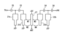
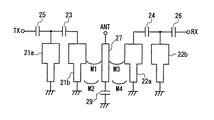
図3に、上記のような構成を有する共用器の等価回路を示す。図3に示すように、本実施の形態の共用器は、段間結合容量23、24と、入出力結合容量25、26と、結合線路27と、共振器21a、21b、22a、22bとを含んでいる。ここで、結合線路27と、当該結合線路27に近接する共振器21bの幅広部とは、電磁界結合M1によって結合されている。また、結合線路27と共振器21bの幅狭部とは、電磁界結合M2によって結合されている。結合線路27と、当該結合線路27に近接する共振器22aの幅広部とは、電磁界結合M3によって結合されている。また、結合線路27と共振器22bの幅狭部とは、電磁界結合M4によって結合されている。
FIG. 3 shows an equivalent circuit of the duplexer having the above configuration. As shown in FIG. 3, the duplexer according to the present embodiment includes
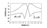
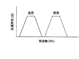
図4に、上記のような構成を有する共用器の伝達特性を示す。図4中、TX→ANTは送信フィルタの特性を表わし、ANT→RXは受信フィルタの特性を表わしている。図4に示すように、本実施の形態の共用器は、送信時において、必要な周波数成分のみを透過し、不要な周波数成分は透過させないことが分かる。また、本実施の形態の共用器は、受信時において、必要な周波数成分のみを透過し、不要な周波数成分は透過させないことが分かる。従って、本実施の形態の共用器を用いれば、送信時に、受信側へ周波数成分が行くのを防止し、受信時に、送信側へ周波数成分が行くのを防止することができる。 FIG. 4 shows the transfer characteristics of the duplexer having the above configuration. In FIG. 4, TX → ANT indicates the characteristics of the transmission filter, and ANT → RX indicates the characteristics of the reception filter. As shown in FIG. 4, it can be seen that the duplexer of the present embodiment transmits only necessary frequency components and does not transmit unnecessary frequency components during transmission. Also, it can be seen that the duplexer of the present embodiment transmits only necessary frequency components and does not transmit unnecessary frequency components at the time of reception. Therefore, by using the duplexer of the present embodiment, it is possible to prevent a frequency component from going to the receiving side during transmission and prevent a frequency component from going to the transmitting side during reception.
本実施の形態の変形として、図5に示すように、誘電体層1bを介在させて結合線路9及びストリップ線路共振器3b、4aと重なるように結合コンデンサ18を設けるのも望ましい。この構成によれば、結合コンデンサ18によって生じる電界結合と、ストリップ線路共振器3b、4aと結合線路9との間に生じる電磁界結合とが組み合わされる。ストリップ線路共振器3b、4aと結合線路9との間に生じる電磁界結合は、磁界成分が支配的であるが、結合コンデンサ18を設けることにより、電界容量成分を増やすことができる。
As a modification of the present embodiment, as shown in FIG. 5, it is desirable to provide a
尚、本実施の形態においては、第1のフィルタが、一端が短絡した2つの第1ストリップ線路共振器3a、3bを含むように構成され、第2のフィルタが、一端が短絡した2つの第2ストリップ線路共振器4a、4bを含むように構成されているが、必ずしもこの構成に限定されるものではない。第1のフィルタは、一端が短絡した第1ストリップ線路共振器を少なくとも1つ含んでいれば足り、第2のフィルタは、一端が短絡した第2ストリップ線路共振器を少なくとも1つ含んでいれば足りる。
In the present embodiment, the first filter is configured to include two
また、本実施の形態においては、第1ストリップ線路共振器3a、3bと第2ストリップ線路共振器4a、4bの双方とも、開放端側で広く、短絡端側で狭い線路幅を有するように構成されているが、必ずしもこの構成に限定されるものではなく、第1ストリップ線路共振器と第2ストリップ線路共振器の少なくとも一方が、開放端側で広く、短絡端側で狭い線路幅を有していればよい。
In the present embodiment, both the
[第2の実施の形態]
図6は本発明の第2の実施の形態における共用器を示す分解斜視図である。本実施の形態の共用器は、以下の点を除いて、上記第1の実施の形態の共用器と同一であるため、同一又は相当する部分には同一の参照番号を付して、その説明は省略する。
[Second embodiment]
FIG. 6 is an exploded perspective view showing a duplexer according to the second embodiment of the present invention. Since the duplexer of the present embodiment is the same as the duplexer of the first embodiment except for the following points, the same or corresponding parts have the same reference characters allotted. Is omitted.
図6に示すように、本実施の形態の共用器においては、第1ストリップ線路共振器3a、3bと第2ストリップ線路共振器4a、4bが、それぞれ、結合線路9が形成された誘電体層1dとは異なる誘電体層1c、1eに形成されている。このように、第1ストリップ線路共振器3a、3bと第2ストリップ線路共振器4a、4bを、それぞれ、結合線路9が形成された誘電体層1dとは異なる誘電体層1c、1eに形成することにより、設計の自由度、融通性を持たせることができる。
As shown in FIG. 6, in the duplexer of the present embodiment, the first
また、結合線路9は、互いに連結された、線路幅の異なる2つのストリップ線路(幅広部と幅狭部)により構成されている。このように、結合線路9を、線路幅の異なる2つのストリップ線路を用いて構成することにより、電磁界結合の強さを任意に変更することができる。
{Circle around (1)} The
尚、本実施の形態においては、第1ストリップ線路共振器3a、3bと第2ストリップ線路共振器4a、4bのそれぞれが、結合線路9が形成された誘電体層1dとは異なる誘電体層1c、1eに形成されているが、必ずしもこの構成に限定されるものではない。第1ストリップ線路共振器と第2ストリップ線路共振器の少なくとも一方が、結合線路が形成された誘電体層とは異なる誘電体層に形成されていればよい。
In the present embodiment, each of the
また、本実施の形態においては、結合線路9が、互いに連結された、線路幅の異なる2つのストリップ線路により構成されているが、必ずしもこの構成に限定されるものではない。結合線路は、互いに連結された、線路幅の異なる3つ以上のストリップ線路により構成されていてもよい。
Also, in the present embodiment, the
[第3の実施の形態]
図7は本発明の第3の実施の形態における共用器を示す分解斜視図である。本実施の形態の共用器は、以下の点を除いて、上記第2の実施の形態の共用器と同一であるため、同一又は相当する部分には同一の参照番号を付して、その説明は省略する。
[Third Embodiment]
FIG. 7 is an exploded perspective view showing a duplexer according to the third embodiment of the present invention. Since the duplexer of the present embodiment is the same as the duplexer of the second embodiment except for the following points, the same or corresponding parts have the same reference characters allotted, and will not be described. Is omitted.
図7に示すように、本実施の形態の共用器においては、結合線路が、3本のストリップ線路9a、9b、9cからなり、3本のストリップ線路9a、9b、9cは、それぞれ異なる誘電体層1c、1d、1eに設けられている。ストリップ線路が1本だけの場合には、電位がふらつくが、3本のストリップ線路を用いることにより、電位の安定化を図ることができる。
As shown in FIG. 7, in the duplexer according to the present embodiment, the coupling line includes three
3本のストリップ線路9a、9b、9cのうち少なくとも1つは、他のストリップ線路と異なる線路幅を有しているのが望ましい。本実施の形態においては、全てのストリップ線路9a、9b、9cの線路幅が異なるように構成されている。電磁界結合は、結合線路の線路幅によっても変わるので、結合線路の線路幅を異ならせることにより、より強い電磁界結合を得ることが可能となる。
It is desirable that at least one of the three
尚、本実施の形態においては、結合線路が、3本のストリップ線路9a、9b、9cにより構成されているが、必ずしもこの構成に限定されるものではなく、結合線路は複数本のストリップ線路により構成されていればよい。
In the present embodiment, the coupling line is constituted by three
[第4の実施の形態]
図8は本発明の第4の実施の形態における共用器を示す分解斜視図である。本実施の形態の共用器は、以下の点を除いて、上記第3の実施の形態の共用器と同一であるため、同一又は相当する部分には同一の参照番号を付して、その説明は省略する。
[Fourth Embodiment]
FIG. 8 is an exploded perspective view showing a duplexer according to the fourth embodiment of the present invention. Since the duplexer of this embodiment is the same as the duplexer of the third embodiment except for the following points, the same or corresponding parts are denoted by the same reference numerals, and the description thereof will be omitted. Is omitted.
図8に示すように、本実施の形態の共用器においては、3本のストリップ線路9a、9b、9cが、ビアホール12によって互いに接続されている。
に お い て As shown in FIG. 8, in the duplexer of the present embodiment, three
本実施の形態の構成によれば、ビアホール12のシールド効果により、第1ストリップ線路共振器3a、3bと第2ストリップ線路共振器4a、4bを分離することができるので、送信時に、受信側へ周波数成分が行くのを防止し、受信時に、送信側へ周波数成分が行くのを防止することができる。
According to the configuration of the present embodiment, the
[第5の実施の形態]
図9は本発明の第5の実施の形態における共用器を示す分解斜視図である。
[Fifth Embodiment]
FIG. 9 is an exploded perspective view showing a duplexer according to the fifth embodiment of the present invention.
図9に示すように、本実施の形態における共用器は、誘電体層と電極層が交互に積層された積層体により構成されている。積層体内には、第3シールド電極32cを介在させて、互いに通過帯域周波数の異なる、送信用の第1のフィルタと受信用の第2のフィルタとが対向して設けられている。また、第1のフィルタと第2のフィルタとの間には、一端が短絡し、他端が外部端子に接続された結合線路39からなる整合回路が設けられている。
As shown in FIG. 9, the duplexer according to the present embodiment is configured by a laminate in which dielectric layers and electrode layers are alternately laminated. In the laminated body, a first filter for transmission and a second filter for reception having different passband frequencies are provided to face each other with a
第1のフィルタは、一端が短絡した2つの第1ストリップ線路共振器33a、33bを含んでいる。また、第2のフィルタは、一端が短絡した2つの第2ストリップ線路共振器34a、34bを含んでいる。結合線路39と第1ストリップ線路共振器33bとは、電磁界結合によって結合されている。また、結合線路39と第2ストリップ線路共振器34bとは、電磁界結合によって結合されている。
1The first filter includes two
次に、本実施の形態における共用器の実際の構造について、さらに詳細に説明する。 Next, the actual structure of the duplexer according to the present embodiment will be described in more detail.
前記積層体は、順次積層された、第1誘電体層31aと、第2誘電体層31bと、第3誘電体層31cと、第4誘電体層31dと、第5誘電体層31eと、第6誘電体層31fとを含んでいる。
The laminated body includes a first
前記電極層は、以下のような構成となっている。すなわち、第1誘電体層31aの上面には、第1シールド電極32aが配置されている。第1誘電体層31aと第2誘電体層31bとの間には、第1のフィルタを構成する、段間結合容量電極35及び入出力結合容量電極37が配置されている。第2誘電体層31bと第3誘電体層31cとの間には、第1のフィルタを構成する第1共振器電極33a、33bが配置されている。第3誘電体層31cと第4誘電体層31dとの間には、第3のシールド電極32cと、整合回路を構成する結合線路電極39とが配置されている。第4誘電体層31dと第5誘電体層31eとの間には、第2のフィルタを構成する、第2共振器電極34a、34b及び共振器電極34aに接続された入出力線路電極38が配置されている。第5誘電体層31eと第6誘電体層31fとの間には、第2のフィルタを構成する段間結合容量電極36が配置されている。第6誘電体層31fの下面には、第2シールド電極32bが配置されている。第1誘電体層31a、第2誘電体層31b、第3誘電体層31c、第4誘電体層31d、第5誘電体層31e及び第6誘電体層31fの側面には、入出力結合容量電極37と入出力線路電極38と結合線路電極39のそれぞれに接続される少なくとも3つの端子電極40a、40b(入出力結合容量電極37、入出力線路電極38に対応する端子電極は図示せず)が設けられている。第1シールド電極32aと第2シールド電極32bと第3シールド電極32cは、端面電極41によって接続されている。
The electrode layer has the following configuration. That is, the
本実施の形態の構成によれば、送信用の第1のフィルタと受信用の第2のフィルタを縦方向(積層方向)に並べることができるので、共用器の占有面積を小さくすることができる。本実施の形態の共用器は、積層構造ゆえに、このような縦積みが可能となる。 According to the configuration of the present embodiment, the first filter for transmission and the second filter for reception can be arranged in the vertical direction (stacking direction), so that the occupied area of the duplexer can be reduced. . Since the duplexer of the present embodiment has a laminated structure, such vertical stacking is possible.
尚、本実施の形態においては、第1のフィルタが、一端が短絡した2つの第1ストリップ線路共振器33a、33bを含むように構成され、第2のフィルタが、一端が短絡した2つの第2ストリップ線路共振器34a、34bを含むように構成されているが、必ずしもこの構成に限定されるものではない。第1のフィルタは、一端が短絡した第1ストリップ線路共振器を3つ以上含んでいてもよく、第2のフィルタは、一端が短絡した第2ストリップ線路共振器を3つ以上含んでいてもよい。
In the present embodiment, the first filter is configured to include two first
[第6の実施の形態]
図10は本発明の第6の実施の形態における共用器を示す分解斜視図である。
[Sixth Embodiment]
FIG. 10 is an exploded perspective view showing a duplexer according to the sixth embodiment of the present invention.
図10に示すように、本実施の形態における共用器は、誘電体層と電極層が交互に積層された積層体により構成されている。積層体内には、第1シールド電極32a、第3シールド電極32c、第4シールド電極32d及び第2シールド電極32bが積層方向に並んで配置されている。第1シールド電極32aと第3シールド電極32cとの間には、一端が短絡した2つの第1ストリップ線路共振器33a、33bが平行に近接して構成された第1のフィルタが設けられている。第3シールド電極32cと第4シールド電極32dとの間には、一端が短絡し、他端が外部端子に接続された結合線路39からなる整合回路が設けられている。第4シールド電極32dと第2シールド電極32bとの間には、一端が短絡した2つの第2ストリップ線路共振器34a、34bが平行に近接して構成され、前記第1のフィルタと通過帯域周波数の異なる第2のフィルタが設けられている。第3シールド電極32cと第4シールド電極32dには、それぞれ結合窓42a、42bが設けられている。そして、第1のフィルタを構成する第1ストリップ線路共振器33bと結合線路39とが、結合窓42aを介して、電磁界結合によって結合されている。また、第2のフィルタを構成する第2ストリップ線路共振器34bと結合線路39とが、結合窓42bを介して、電磁界結合によって結合されている。
As shown in FIG. 10, the duplexer according to the present embodiment is configured by a laminate in which dielectric layers and electrode layers are alternately laminated. The
結合窓42a、42bはシールド電極が印刷されていない部分であり、このような結合窓42a、42bを設けることにより、電磁界結合の強さの融通性を、簡単に図ることができる。
(4) The
次に、本実施の形態における共用器の実際の構造について、さらに詳細に説明する。 Next, the actual structure of the duplexer according to the present embodiment will be described in more detail.
前記積層体は、順次積層された、第1誘電体層31aと、第2誘電体層31bと、第3誘電体層31cと、第4誘電体層31gと、第5誘電体層31hと、第6誘電体層31dと、第7誘電体層31eと、第8誘電体層31fとを含んでいる。
The laminate includes a first
前記電極層は、以下のような構成となっている。すなわち、第1誘電体層31aの上面には、第1シールド電極32aが配置されている。第1誘電体層31aと第2誘電体層31bとの間には、第1のフィルタを構成する、段間結合容量電極35及び入出力結合容量電極37とが配置されている。また、第2誘電体層31bと第3誘電体層31cとの間には、第1のフィルタを構成する第1共振器電極33a、33bが配置されている。第3誘電体層31cと第4誘電体層31gとの間には、一部に結合窓42aが設けられた第3シールド電極32cが配置されている。第4誘電体層31gと第5誘電体層31hとの間には、一端が短絡し、他端が外部端子に接続された、整合回路を構成する結合線路電極39が配置されている。第5誘電体層31hと第6誘電体層31dとの間には、一部に結合窓42bが設けられた第4シールド電極32dが配置されている。第6誘電体層31dと第7誘電体層31eとの間には、第2のフィルタを構成する、第2共振器電極34a、34b及び共振器電極34aに接続された入出力線路電極38が配置されている。また、第7誘電体層31eと第8誘電体層31fとの間には、第2のフィルタを構成する段間結合容量電極36が配置されている。第8誘電体層31fの下面には、第2シールド電極32bが配置されている。第1誘電体層31a、第2誘電体層31b、第3誘電体層31c、第4誘電体層31g、第5誘電体層31h、第6誘電体層31d、第7誘電体層31e及び第8誘電体層31fの側面には、入出力結合容量電極37と入出力線路電極38と結合線路電極39のそれぞれに接続される少なくとも3つの端子電極40a、40bが設けられている(入出力結合容量電極37、入出力線路電極38に対応する端子電極は図示せず)。第1シールド電極32aと第3シールド電極32cと第4シールド電極32dと第2シールド電極32bは、端面電極41によって接続されている。
The electrode layer has the following configuration. That is, the
本実施の形態の構成によれば、誘電体層の上にシールド電極を印刷するときに、その一部を印刷せずに結合窓42a、42bを設ける、という簡単な方法により、電磁界結合の強さを容易に変えることができる。
According to the configuration of the present embodiment, when the shield electrode is printed on the dielectric layer, the
図11に、上記のような構成を有する共用器の等価回路を示す。本実施の形態における共用器の等価回路は、以下の点を除いて、図3に示す等価回路と同一であるため、同一又は相当する部分には同一の参照番号を付して、その説明は省略する。 FIG. 11 shows an equivalent circuit of a duplexer having the above configuration. Since the equivalent circuit of the duplexer in the present embodiment is the same as the equivalent circuit shown in FIG. 3 except for the following points, the same or corresponding parts are denoted by the same reference numerals, and the description thereof will be omitted. Omitted.
本実施の形態における共用器の等価回路が図3に示す等価回路と異なる点は、誘電体層を介在させて結合線路27及びストリップ線路共振器21bと重なるように結合コンデンサ28aが設けられ、誘電体層を介在させて結合線路27及びストリップ線路共振器22aと重なるように結合コンデンサ28bが設けられている点である。これにより、結合コンデンサ28a、28bによって生じる電界結合と、ストリップ線路共振器22a、21bと結合線路27との間に生じる電磁界結合とが組み合わされる。ストリップ線路共振器22a、21bと結合線路27との間に生じる電磁界結合は、磁界成分が支配的であるが、結合コンデンサ28a、28bを設けることにより、電界容量成分を増やすことができる。
3 is different from the equivalent circuit shown in FIG. 3 in that a
[第7の実施の形態]
図12は本発明の第7の実施の形態における共用器を示す分解斜視図である。本実施の形態における共用器は、以下の点を除いて、図2に示す上記第1の実施の形態の共用器と同一であるため、同一又は相当する部分には同一の参照番号を付して、その説明は省略する。
[Seventh Embodiment]
FIG. 12 is an exploded perspective view showing a duplexer according to the seventh embodiment of the present invention. Since the duplexer in the present embodiment is the same as the duplexer of the first embodiment shown in FIG. 2 except for the following points, the same or corresponding parts are denoted by the same reference numerals. Therefore, the description is omitted.
図12に示すように、本実施の形態の共用器においては、第1誘電体層1aを間に挟んで、第1シールド電極2aと対向させて調整用容量電極13が設けられている。アンテナは、送信と受信の双方に用いられるが、調整用容量電極13を設けることにより、送信と受信の整合を最適化することができる。
示 す As shown in FIG. 12, in the duplexer of the present embodiment, the adjusting
[第8の実施の形態]
図13は本発明の第8の実施の形態における共用器を示す分解斜視図である。本実施の形態における共用器は、以下の点を除いて、図2に示す上記第1の実施の形態の共用器と同一であるため、同一又は相当する部分には同一の参照番号を付して、その説明は省略する。
[Eighth Embodiment]
FIG. 13 is an exploded perspective view showing a duplexer according to the eighth embodiment of the present invention. Since the duplexer in the present embodiment is the same as the duplexer of the first embodiment shown in FIG. 2 except for the following points, the same or corresponding parts are denoted by the same reference numerals. Therefore, the description is omitted.
図13に示すように、本実施の形態の共用器においては、第1のフィルタと第2のフィルタとの間に、一端が開放し、他端が外部端子に接続された結合線路9からなる整合回路が設けられている。このように、一端が開放し、他端が外部端子に接続された結合線路9を用いることによっても、共用器として動作させることができる。
As shown in FIG. 13, in the duplexer of the present embodiment, between the first filter and the second filter, one end is open and the other end is formed of a
本実施の形態の変形として、図14に示すように、結合線路9の開放端側に、第3誘電体層1cを介在させて整合用容量電極14を設けるのも望ましい。結合線路9の一端を開放した場合には、開放端に浮遊容量が生じ、容量のばらつきの要因となるが、結合線路9の開放端側に、第3誘電体層1cを介在させて整合用容量電極14を設けることにより、容量値を安定化させることができる。また、整合用容量の容量値を変えることにより、設計の自由度を得ることができる。
As a modification of the present embodiment, as shown in FIG. 14, it is also desirable to provide a
図15に、図14に示す共用器の等価回路を示す。図15に示す等価回路は、以下の点を除いて、図3に示す等価回路と同一であるため、同一又は相当する部分には同一の参照番号を付して、その説明は省略する。 FIG. 15 shows an equivalent circuit of the duplexer shown in FIG. The equivalent circuit shown in FIG. 15 is the same as the equivalent circuit shown in FIG. 3 except for the following points. Therefore, the same or corresponding portions are denoted by the same reference numerals and description thereof will be omitted.
図15に示す等価回路が図3に示す等価回路と異なる点は、結合線路27の開放端側に整合用容量29が設けられている点である。
3 is different from the equivalent circuit shown in FIG. 3 in that a matching
また、本実施の形態の変形として、上記第2〜第5又は第7の実施の形態に示した構成とするのも望ましい。 Further, as a modification of the present embodiment, it is also desirable to adopt the configuration shown in the second to fifth or seventh embodiments.
[第9の実施の形態]
図16は本発明の第9の実施の形態における共用器を示す分解斜視図である。
[Ninth embodiment]
FIG. 16 is an exploded perspective view showing a duplexer according to the ninth embodiment of the present invention.
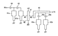
図16に示すように、本実施の形態における共用器は、誘電体層と電極層が交互に積層された積層体により構成されている。積層体内には、互いに通過帯域周波数の異なる、送信用の第1のフィルタと受信用の第2のフィルタとが設けられている。第1及び第2のフィルタのうちの少なくとも一方(本実施の形態においては、第2のフィルタ)は、帯域阻止特性を有する、一端が短絡した第2ストリップ線路共振器54a、54bと伝送線路57とからなるフィルタである。第1のフィルタと第2のフィルタとの間には、一端が短絡し、他端が外部端子に接続された、結合線路58a、58bからなる整合回路が設けられている。伝送線路57と結合線路58bは、電磁界結合によって結合されている。
共用 As shown in FIG. 16, the duplexer in the present embodiment is configured by a laminate in which dielectric layers and electrode layers are alternately laminated. A first filter for transmission and a second filter for reception having different passband frequencies are provided in the laminate. At least one of the first and second filters (the second filter in the present embodiment) is a
次に、本実施の形態における共用器の実際の構造について、さらに詳細に説明する。 Next, the actual structure of the duplexer according to the present embodiment will be described in more detail.
前記積層体は、順次積層された、第1誘電体層51aと、第2誘電体層51bと、第3誘電体層51cと、第4誘電体層51dと、第5誘電体層51eとを含んでいる。
The laminate includes a first
前記電極層は、以下のような構成となっている。すなわち、第1誘電体層51aの上面には、第1シールド電極52aが配置されている。第1誘電体層51aと第2誘電体層51bとの間には、第1のフィルタを構成する段間結合容量電極55が配置されている。第2誘電体層51bと第3誘電体層51cとの間には、第1のフィルタを構成する第1共振器電極53a、53bと、整合回路を構成する結合線路電極58aとが配置されている。第3誘電体層51cと第4誘電体層51dとの間には、第1のフィルタを構成する入出力結合容量電極56と、帯域阻止特性を有する第2フィルタを構成する伝送線路電極57と、整合回路を構成する結合線路電極58bとが配置されている。第4誘電体層51dと第5誘電体層51eとの間には、第2のフィルタを構成する第2共振器電極54a、54bが配置されている。第5の誘電体層51eの下面には、第2のシールド電極52bが配置されている。第1誘電体層51a、第2誘電体層51b、第3誘電体層51c、第4誘電体層51d及び第5誘電体層51eの側面には、入出力結合容量電極56と伝送線路電極57と結合線路電極58a、58bのそれぞれに接続される少なくとも3つの端子電極59a、59b(入出力結合容量電極56に対応する端子電極は図示せず)が設けられている。第1シールド電極52aと第2シールド電極52bは、端面電極60a、60bによって接続されている。
The electrode layer has the following configuration. That is, the
本実施の形態の構成によれば、上記のような積層構造とすることにより、帯域阻止特性を有するフィルタを、容易に形成することができる。 According to the configuration of the present embodiment, a filter having band rejection characteristics can be easily formed by adopting the above-described laminated structure.
図17に、上記のような構成を有する共用器の等価回路を示す。図17に示すように、本実施の形態の共用器は、段間結合容量63と、入出力結合容量64と、伝送線路65とを含んでいる。第1のフィルタは、共振器61a、61bを含んでいる。共振器62aはノッチ容量66aを介して伝送線路65に接続され、共振器62bはノッチ容量66bを介して伝送線路65に接続されている。
FIG. 17 shows an equivalent circuit of a duplexer having the above configuration. As shown in FIG. 17, the duplexer of the present embodiment includes an
図18に、上記のような構成を有する共用器の伝達特性を示す。本実施の形態においては、送信用の第2のフィルタが、帯域阻止特性を有する、一端が短絡した第2ストリップ線路共振器54a、54bと伝送線路57とにより構成されているので、特定の高周波成分のみを阻止するフィルタとなる。帯域阻止特性を有するフィルタは、帯域通過特性を有するフィルタに比べて、低損失化を図ることができるので、送信フィルタの損失を低減することが可能となる。
FIG. 18 shows the transfer characteristics of the duplexer having the above configuration. In the present embodiment, the second filter for transmission is constituted by the
本実施の形態の変形として、図19に示すように、第1のフィルタと第2のフィルタとの間に、一端が開放し、他端が外部端子に接続された、結合線路58a、58bからなる整合回路を設けることによっても、同様の効果が得られる。
As a modification of the present embodiment, as shown in FIG. 19, between the first filter and the second filter, one end is opened and the other end is connected to an external terminal from the
図20に、図19に示す共用器の等価回路を示す。 FIG. 20 shows an equivalent circuit of the duplexer shown in FIG.
尚、本実施の形態においては、第1のフィルタが、一端が短絡した2つの第1ストリップ線路共振器53a、53bを含むように構成され、第2のフィルタが、一端が短絡した2つの第2ストリップ線路共振器54a、54bを含むように構成されているが、必ずしもこの構成に限定されるものではない。第1のフィルタは、一端が短絡した第1ストリップ線路共振器を3つ以上含んでいてもよく、第2のフィルタは、一端が短絡した第2ストリップ線路共振器を3つ以上含んでいてもよい。
In the present embodiment, the first filter is configured to include the two
[第10の実施の形態]
図21は本発明の第10の実施の形態における共用器を示す分解斜視図である。本実施の形態における共用器は、上記第9の実施の形態における共用器の変形例である。
[Tenth embodiment]
FIG. 21 is an exploded perspective view showing a duplexer according to the tenth embodiment of the present invention. The duplexer in the present embodiment is a modified example of the duplexer in the ninth embodiment.
図21に示すように、積層体は、順次積層された、第1誘電体層51aと、第2誘電体51bと、第3誘電体層51cと、第4誘電体層51dと、第5誘電体層51eとを含んでいる。
As shown in FIG. 21, the laminated body is formed by sequentially laminating a first
電極層は、以下のような構成となっている。すなわち、第1誘電体層51aの上面には、第1シールド電極52aが配置されている。第1誘電体層51aと第2誘電体層51bとの間には、第1のフィルタを構成する段間結合容量電極55が配置されている。第2誘電体層51bと第3誘電体層51cとの間には、第1のフィルタを構成する第1共振器電極53a、53bと、整合回路を構成する結合線路電極58cとが配置されている。また、第3誘電体層51cと第4誘電体層51dとの間には、第1のフィルタを構成する入出力結合容量電極56と、帯域阻止特性を有する第2フィルタを構成する伝送線路電極57とが配置されている。第4誘電体層51dと第5誘電体層51eとの間には、第2のフィルタを構成する第2共振器電極54a、54bが配置されている。第5の誘電体層51eの下面には、第2のシールド電極52bが配置されている。第1誘電体層51a、第2誘電体層51b、第3誘電体層51c、第4誘電体層51d及び第5誘電体層51eの側面には、入出力結合容量電極56と伝送線路電極57と結合線路電極58cにそれぞれ接続される少なくとも3つの端子電極59a、59b(入出力結合容量電極56に対応する端子電極は図示せず)が設けられている。第1シールド電極52aと第2シールド電極52bは、端面電極60a、60bによって接続されている。
The electrode layer has the following configuration. That is, the
伝送線路電極57の一部分57aは、積層方向への投影において、第3誘電体層51cを介在させて結合線路電極58cと重なっており、積層方向への投影において、伝送線路電極57の一部分57aの幅は、結合線路電極58cの幅と異なっている。
The
本実施の形態の構成によれば、結合線路電極58cと伝送線路電極57を縦方向に上下に配置しているので、電磁界結合がより強くなる。また、伝送線路電極57の一部分57aの幅を、結合線路電極58cの幅と異ならせることにより、積層時に重なり合いのずれに対して余裕を持たせることができる。尚、伝送線路電極57の一部分57aの幅は、結合線路電極58cの幅と同一であってもよい。
According to the configuration of the present embodiment, since the
[第11の実施の形態]
図22は本発明の第11の実施の形態における積層型高周波デバイスを示す概略斜視図である。図22に示すように、本実施の形態の積層型高周波デバイスは、誘電体層と電極層が交互に積層された積層体71からなる共用器を備えている。積層体71の上面には、半導体チップ72、弾性表面波デバイス73、PINダイオード74、チップコンデンサ75及びチップ抵抗76が実装されている。
[Eleventh embodiment]
FIG. 22 is a schematic perspective view showing a laminated high-frequency device according to the eleventh embodiment of the present invention. As shown in FIG. 22, the multilayer high-frequency device according to the present embodiment includes a duplexer including a
前記共用器としては、上記各実施の形態で説明した構造を有する共用器が用いられている。例えば、積層体71内には、互いに通過帯域周波数の異なる、送信用の第1のフィルタと受信用の第2のフィルタとが設けられている。第1のフィルタと第2のフィルタとの間には、一端が短絡し、他端が外部端子に接続された結合線路からなる整合回路が設けられている。第1のフィルタは、一端が短絡した第1ストリップ線路共振器を少なくとも1つ含んでいる。第2のフィルタは、一端が短絡した第2ストリップ線路共振器を少なくとも1つ含んでいる。第1ストリップ線路共振器と第2ストリップ線路共振器は、それぞれ前記結合線路と電磁界結合によって結合されている。
共用 As the duplexer, a duplexer having the structure described in each of the above embodiments is used. For example, a first filter for transmission and a second filter for reception having different passband frequencies are provided in the stacked
本実施の形態の構成によれば、共用器を非常に簡単な構造で実現することができるので、大幅な低損失化が可能な、半導体チップ及び/又は弾性表面波デバイスを備えた、積層型高周波デバイスを得ることができる。 According to the configuration of the present embodiment, since the duplexer can be realized with a very simple structure, a laminated type including a semiconductor chip and / or a surface acoustic wave device capable of significantly reducing loss can be provided. A high-frequency device can be obtained.
[第12の実施の形態]
図23は本発明の第12の実施の形態における通信機器を示す模式図である。
[Twelfth embodiment]
FIG. 23 is a schematic diagram showing a communication device according to the twelfth embodiment of the present invention.
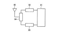
図23に示すように、本実施の形態における通信機器は、アンテナ85と、送信回路から出た周波数成分をアンテナ85に送り、かつ、アンテナ85から受信した周波数成分を受信回路に送る、誘電体層と電極層が交互に積層された積層体からなる共用器84を備えている。共用器84は、送信回路部82及び受信回路部83に接続され、送信回路部82と受信回路部83は、ベースバンド部81に接続されている。
As shown in FIG. 23, the communication device according to the present embodiment is a dielectric device that transmits an
共用器84としては、上記各実施の形態で説明した構造を有する共用器が用いられている。例えば、積層体内には、互いに通過帯域周波数の異なる、送信用の第1のフィルタと受信用の第2のフィルタとが設けられている。第1のフィルタと第2のフィルタとの間には、一端が短絡し、他端が外部端子に接続された結合線路からなる整合回路が設けられている。第1のフィルタは、一端が短絡した第1ストリップ線路共振器を少なくとも1つ含んでいる。第2のフィルタは、一端が短絡した第2ストリップ線路共振器を少なくとも1つ含んでいる。第1ストリップ線路共振器と第2ストリップ線路共振器は、それぞれ前記結合線路と電磁界結合によって結合されている。
共用 As the
本実施の形態の構成によれば、共用器を非常に簡単な構造で実現することができるので、大幅な低損失化が可能な通信機器を得ることができる。 According to the configuration of the present embodiment, since the duplexer can be realized with a very simple structure, it is possible to obtain a communication device capable of greatly reducing loss.
尚、本実施の形態の変形として、前記積層体の上面に、半導体チップ及び/又は弾性表面波デバイスが実装されていてもよい。この構成によれば、大幅な低損失化が可能な、半導体チップ及び/又は弾性表面波デバイスを備えた、積層型高周波デバイスを含む通信機器を得ることができる。 As a modification of the present embodiment, a semiconductor chip and / or a surface acoustic wave device may be mounted on the upper surface of the laminate. According to this configuration, it is possible to obtain a communication device including a stacked high-frequency device provided with a semiconductor chip and / or a surface acoustic wave device, which can significantly reduce the loss.
1a、1b、1c、1d 誘電体層
3a、3b 第1ストリップ線路共振器
4a、4b 第2第1ストリップ線路共振器
9 結合線路
1a, 1b, 1c,
Claims (35)
前記積層体内に設けられ、互いに通過帯域周波数の異なる、送信用の第1のフィルタと受信用の第2のフィルタと、
前記第1のフィルタと前記第2のフィルタとの間に設けられ、一端が短絡し、他端が外部端子に接続された結合線路からなる整合回路とを備え、
前記第1のフィルタは、一端が短絡した第1ストリップ線路共振器を少なくとも1つ含み、
前記第2のフィルタは、一端が短絡した第2ストリップ線路共振器を少なくとも1つ含み、
前記第1ストリップ線路共振器と前記第2ストリップ線路共振器は、それぞれ前記結合線路と電磁界結合によって結合されていることを特徴とする共用器。 A duplexer comprising a laminate in which dielectric layers and electrode layers are alternately laminated,
A first filter for transmission and a second filter for reception provided in the laminate and having different passband frequencies from each other;
A matching circuit provided between the first filter and the second filter, the one end being short-circuited, and the other end including a coupling line connected to an external terminal;
The first filter includes at least one first stripline resonator having one end short-circuited,
The second filter includes at least one second stripline resonator having one end short-circuited,
The duplexer, wherein the first stripline resonator and the second stripline resonator are respectively coupled to the coupling line by electromagnetic coupling.
前記電極層は、
前記第1誘電体層の上面に配置された第1シールド電極と、
前記第1誘電体層と前記第2誘電体層との間に配置された、前記第1のフィルタを構成する段間結合容量電極と、前記第2のフィルタを構成する入出力結合容量電極と、
前記第2誘電体層と前記第3誘電体層との間に配置された、前記第1のフィルタを構成する第1共振器電極と、前記第2のフィルタを構成する第2共振器電極と、前記整合回路を構成する結合線路電極と、
前記第3誘電体層と前記第4誘電体層との間に配置された、前記第1のフィルタを構成する入出力結合容量電極と、前記第2のフィルタを構成する段間結合容量電極と、
前記第4誘電体層の下面に配置された第2シールド電極と、
前記第1誘電体層、第2誘電体層、第3誘電体層及び第4誘電体層の側面に設けられ、前記第1のフィルタを構成する前記入出力結合容量電極と前記第2のフィルタを構成する前記入出力結合容量電極と前記結合線路電極のそれぞれに接続された少なくとも3つの端子電極と、
前記第1シールド電極と前記第2シールド電極とを接続する端面電極とを含む請求項1に記載の共用器。 The laminate includes a first dielectric layer, a second dielectric layer, a third dielectric layer, and a fourth dielectric layer, which are sequentially laminated.
The electrode layer,
A first shield electrode disposed on an upper surface of the first dielectric layer;
An inter-stage coupling capacitance electrode configuring the first filter, disposed between the first dielectric layer and the second dielectric layer; and an input / output coupling capacitance electrode configuring the second filter. ,
A first resonator electrode forming the first filter and a second resonator electrode forming the second filter, disposed between the second dielectric layer and the third dielectric layer; A coupling line electrode constituting the matching circuit;
An input / output coupling capacitance electrode constituting the first filter, an inter-stage coupling capacitance electrode constituting the second filter, disposed between the third dielectric layer and the fourth dielectric layer; ,
A second shield electrode disposed on a lower surface of the fourth dielectric layer;
The input / output coupling capacitance electrode provided on a side surface of the first dielectric layer, the second dielectric layer, the third dielectric layer, and the fourth dielectric layer, and constituting the first filter; and the second filter At least three terminal electrodes connected to the input / output coupling capacitance electrode and the coupling line electrode, respectively.
2. The duplexer according to claim 1, further comprising an end face electrode connecting the first shield electrode and the second shield electrode. 3.
前記電極層は、
前記第1誘電体層の上面に配置された第1シールド電極と、
前記第1誘電体層と前記第2誘電体層との間に配置された、前記第1のフィルタを構成する、段間結合容量電極及び入出力結合容量電極と、
前記第2誘電体層と前記第3誘電体層との間に配置された、前記第1のフィルタを構成する複数個の共振器電極と、
前記第3誘電体層と前記第4誘電体層との間に配置された、第3のシールド電極と、前記整合回路を構成する結合線路電極と、
前記第4誘電体層と前記第5誘電体層との間に配置された、前記第2のフィルタを構成する、複数個の共振器電極及び当該共振器電極に接続された入出力線路電極と、
前記第5誘電体層と前記第6誘電体層との間に配置された、前記第2のフィルタを構成する段間結合容量電極と、
前記第6誘電体層の下面に配置された第2シールド電極と、
前記第1誘電体層、第2誘電体層、第3誘電体層、第4誘電体層、第5誘電体層及び第6誘電体層の側面に設けられ、前記入出力結合容量電極と前記入出力線路電極と前記結合線路電極のそれぞれに接続された少なくとも3つの端子電極と、
前記第1シールド電極と前記第2シールド電極と前記第3シールド電極とを接続する端面電極とを含む請求項12に記載の共用器。 The laminate includes a first dielectric layer, a second dielectric layer, a third dielectric layer, a fourth dielectric layer, a fifth dielectric layer, and a sixth dielectric layer, which are sequentially laminated. And
The electrode layer,
A first shield electrode disposed on an upper surface of the first dielectric layer;
An interstage coupling capacitance electrode and an input / output coupling capacitance electrode, which constitute the first filter, are disposed between the first dielectric layer and the second dielectric layer;
A plurality of resonator electrodes constituting the first filter, disposed between the second dielectric layer and the third dielectric layer;
A third shield electrode disposed between the third dielectric layer and the fourth dielectric layer, and a coupling line electrode forming the matching circuit;
A plurality of resonator electrodes and an input / output line electrode connected to the resonator electrodes, which are arranged between the fourth dielectric layer and the fifth dielectric layer, and constitute the second filter; ,
An inter-stage coupling capacitance electrode constituting the second filter, disposed between the fifth dielectric layer and the sixth dielectric layer;
A second shield electrode disposed on a lower surface of the sixth dielectric layer;
A first dielectric layer, a second dielectric layer, a third dielectric layer, a fourth dielectric layer, a fifth dielectric layer, and a sixth dielectric layer. At least three terminal electrodes connected to each of the writing output line electrode and the coupling line electrode;
The duplexer according to claim 12, further comprising an end face electrode connecting the first shield electrode, the second shield electrode, and the third shield electrode.
前記積層体内に積層方向に並んで配置された第1シールド電極、第2シールド電極、第3シールド電極及び第4シールド電極と、
前記第1シールド電極と第2シールド電極との間に配置され、一端が短絡したストリップ線路共振器が複数個平行に近接して構成された第1のフィルタと、
前記第2シールド電極と第3シールド電極との間に配置され、結合線路からなる整合回路と、
前記第3シールド電極と前記第4シールド電極との間に配置され、一端が短絡したストリップ線路共振器が複数個平行に近接して構成され、前記第1のフィルタと通過帯域周波数の異なる第2のフィルタとを備え、
前記第2及び第3シールド電極には結合窓が設けられ、
前記第1及び第2のフィルタを構成する前記ストリップ線路共振器と前記結合線路とが、それぞれ前記結合窓を介して、電磁界結合によって結合されていることを特徴とする共用器。 A duplexer comprising a laminate in which dielectric layers and electrode layers are alternately laminated,
A first shield electrode, a second shield electrode, a third shield electrode, and a fourth shield electrode arranged in the stack in the stacking direction;
A first filter disposed between the first shield electrode and the second shield electrode, wherein a plurality of stripline resonators having one end short-circuited are arranged in parallel and close to each other;
A matching circuit disposed between the second shield electrode and the third shield electrode, the matching circuit including a coupling line;
A plurality of strip line resonators each of which is disposed between the third shield electrode and the fourth shield electrode, and one end of which is short-circuited, are configured in parallel and close to each other, and have a second pass band frequency different from that of the first filter. With a filter of
A coupling window is provided in the second and third shield electrodes,
A duplexer, wherein the stripline resonators constituting the first and second filters and the coupling line are coupled by electromagnetic coupling through the coupling windows, respectively.
前記電極層は、
前記第1誘電体層の上面に配置された第1シールド電極と、
前記第1誘電体層と前記第2誘電体層との間に配置された、前記第1のフィルタを構成する、段間結合容量電極及び入出力結合容量電極と、
前記第2誘電体層と前記第3誘電体層との間に配置された、前記第1のフィルタを構成する複数個の共振器電極と、
前記第3誘電体層と前記第4誘電体層との間に配置され、一部に前記結合窓が設けられた第3のシールド電極と、
前記第4誘電体層と前記第5誘電体層との間に配置された、前記整合回路を構成する結合線路電極と、
前記第5誘電体層と前記第6誘電体層との間に配置され、一部に前記結合窓が設けられた第4シールド電極と、
前記第6誘電体層と前記第7誘電体層との間に配置され、前記第2のフィルタを構成する、複数個の共振器電極及び当該共振器電極に接続された入出力線路電極と、
前記第7誘電体層と前記第8誘電体層との間に配置された、前記第2のフィルタを構成する段間結合容量電極と、
前記第8の誘電体層の下面に配置された第2のシールド電極と、
前記第1誘電体層、第2誘電体層、第3誘電体層、第4誘電体層、第5誘電体層、第6誘電体層、第7誘電体層及び第8誘電体層の側面に設けられ、前記入出力結合容量電極と前記入出力線路電極と前記結合線路電極のそれぞれに接続された少なくとも3つの端子電極と、
前記第1シールド電極と前記第2シールド電極と前記第3シールド電極と前記第4シールド電極とを接続する端面電極とを含む請求項14に記載の共用器。 The laminate includes a first dielectric layer, a second dielectric layer, a third dielectric layer, a fourth dielectric layer, a fifth dielectric layer, and a sixth dielectric layer, which are sequentially laminated. And a seventh dielectric layer and an eighth dielectric layer,
The electrode layer,
A first shield electrode disposed on an upper surface of the first dielectric layer;
An interstage coupling capacitance electrode and an input / output coupling capacitance electrode, which constitute the first filter, are disposed between the first dielectric layer and the second dielectric layer;
A plurality of resonator electrodes constituting the first filter, disposed between the second dielectric layer and the third dielectric layer;
A third shield electrode disposed between the third dielectric layer and the fourth dielectric layer and partially provided with the coupling window;
A coupling line electrode that is arranged between the fourth dielectric layer and the fifth dielectric layer and that constitutes the matching circuit;
A fourth shield electrode disposed between the fifth dielectric layer and the sixth dielectric layer and partially provided with the coupling window;
A plurality of resonator electrodes and an input / output line electrode connected to the resonator electrodes, which are arranged between the sixth dielectric layer and the seventh dielectric layer and constitute the second filter;
An inter-stage coupling capacitance electrode constituting the second filter, disposed between the seventh dielectric layer and the eighth dielectric layer;
A second shield electrode disposed on a lower surface of the eighth dielectric layer;
Side surfaces of the first dielectric layer, the second dielectric layer, the third dielectric layer, the fourth dielectric layer, the fifth dielectric layer, the sixth dielectric layer, the seventh dielectric layer and the eighth dielectric layer And at least three terminal electrodes respectively connected to the input / output coupling capacitance electrode, the input / output line electrode, and the coupling line electrode;
The duplexer according to claim 14, further comprising an end face electrode connecting the first shield electrode, the second shield electrode, the third shield electrode, and the fourth shield electrode.
前記積層体内に設けられ、互いに通過帯域周波数の異なる、送信用の第1のフィルタと受信用の第2のフィルタと、
前記第1のフィルタと前記第2のフィルタとの間に設けられ、一端が開放し、他端が外部端子に接続された結合線路からなる整合回路とを備え、
前記第1のフィルタは、一端が短絡した第1ストリップ線路共振器を少なくとも1つ含み、
前記第2のフィルタは、一端が短絡した第2ストリップ線路共振器を少なくとも1つ含み、
前記第1ストリップ線路共振器と前記第2ストリップ線路共振器は、それぞれ前記結合線路と電磁界結合によって結合されていることを特徴とする共用器。 A duplexer comprising a laminate in which dielectric layers and electrode layers are alternately laminated,
A first filter for transmission and a second filter for reception provided in the laminate and having different passband frequencies from each other;
A matching circuit provided between the first filter and the second filter, the matching circuit including a coupling line having one end open and the other end connected to an external terminal;
The first filter includes at least one first stripline resonator having one end short-circuited,
The second filter includes at least one second stripline resonator having one end short-circuited,
The duplexer, wherein the first stripline resonator and the second stripline resonator are respectively coupled to the coupling line by electromagnetic coupling.
前記電極層は、
前記第1誘電体層の上面に配置された第1シールド電極と、
前記第1誘電体層と前記第2誘電体層との間に配置された、前記第1のフィルタを構成する段間結合容量電極と、前記第2のフィルタを構成する入出力結合容量電極と、
前記第2誘電体層と前記第3誘電体層との間に配置された、前記第1のフィルタを構成する第1共振器電極と、前記第2のフィルタを構成する第2共振器電極と、前記整合回路を構成する結合線路電極と、
前記第3誘電体層と前記第4誘電体層との間に配置された、前記第1のフィルタを構成する入出力結合容量電極と、前記第2のフィルタを構成する段間結合容量電極と、
前記第4誘電体層の下面に配置された第2シールド電極と、
前記第1誘電体層、第2誘電体層、第3誘電体層及び第4誘電体層の側面に設けられ、前記第1のフィルタを構成する前記入出力結合容量電極と前記第2のフィルタを構成する前記入出力結合容量電極と前記結合線路電極のそれぞれに接続された少なくとも3つの端子電極と、
前記第1シールド電極と前記第2シールド電極とを接続する端面電極とを含む請求項16に記載の共用器。 The laminate includes a first dielectric layer, a second dielectric layer, a third dielectric layer, and a fourth dielectric layer, which are sequentially laminated.
The electrode layer,
A first shield electrode disposed on an upper surface of the first dielectric layer;
An inter-stage coupling capacitance electrode configuring the first filter, disposed between the first dielectric layer and the second dielectric layer; and an input / output coupling capacitance electrode configuring the second filter. ,
A first resonator electrode forming the first filter and a second resonator electrode forming the second filter, disposed between the second dielectric layer and the third dielectric layer; A coupling line electrode constituting the matching circuit;
An input / output coupling capacitance electrode constituting the first filter, an inter-stage coupling capacitance electrode constituting the second filter, disposed between the third dielectric layer and the fourth dielectric layer; ,
A second shield electrode disposed on a lower surface of the fourth dielectric layer;
The input / output coupling capacitance electrode provided on a side surface of the first dielectric layer, the second dielectric layer, the third dielectric layer, and the fourth dielectric layer, and constituting the first filter; and the second filter At least three terminal electrodes connected to the input / output coupling capacitance electrode and the coupling line electrode, respectively.
The duplexer according to claim 16, further comprising an end face electrode connecting the first shield electrode and the second shield electrode.
前記電極層は、
前記第1誘電体層の上面に配置された第1シールド電極と、
前記第1誘電体層と前記第2誘電体層との間に配置された、前記第1のフィルタを構成する、段間結合容量電極及び入出力結合容量電極と、
前記第2誘電体層と前記第3誘電体層との間に配置された、前記第1のフィルタを構成する複数個の共振器電極と、
前記第3誘電体層と前記第4誘電体層との間に配置された、第3のシールド電極と、前記整合回路を構成する結合線路電極と、
前記第4誘電体層と前記第5誘電体層との間に配置された、前記第2のフィルタを構成する、複数個の共振器電極及び当該共振器電極に接続された入出力線路電極と、
前記第5誘電体層と前記第6誘電体層との間に配置された、前記第2のフィルタを構成する段間結合容量電極と、
前記第6誘電体層の下面に配置された第2シールド電極と、
前記第1誘電体層、第2誘電体層、第3誘電体層、第4誘電体層、第5誘電体層及び第6誘電体層の側面に設けられ、前記入出力結合容量電極と前記入出力線路電極と前記結合線路電極のそれぞれに接続された少なくとも3つの端子電極と、
前記第1シールド電極と前記第2シールド電極と前記第3シールド電極とを接続する端面電極とを含む請求項28に記載の共用器。 The laminate includes a first dielectric layer, a second dielectric layer, a third dielectric layer, a fourth dielectric layer, a fifth dielectric layer, and a sixth dielectric layer, which are sequentially laminated. And
The electrode layer,
A first shield electrode disposed on an upper surface of the first dielectric layer;
An interstage coupling capacitance electrode and an input / output coupling capacitance electrode, which are arranged between the first dielectric layer and the second dielectric layer, and constitute the first filter;
A plurality of resonator electrodes constituting the first filter, disposed between the second dielectric layer and the third dielectric layer;
A third shield electrode disposed between the third dielectric layer and the fourth dielectric layer, and a coupling line electrode forming the matching circuit;
A plurality of resonator electrodes and an input / output line electrode connected to the resonator electrodes, which are arranged between the fourth dielectric layer and the fifth dielectric layer, and constitute the second filter; ,
An inter-stage coupling capacitance electrode constituting the second filter, disposed between the fifth dielectric layer and the sixth dielectric layer;
A second shield electrode disposed on a lower surface of the sixth dielectric layer;
A first dielectric layer, a second dielectric layer, a third dielectric layer, a fourth dielectric layer, a fifth dielectric layer, and a sixth dielectric layer. At least three terminal electrodes connected to each of the writing output line electrode and the coupling line electrode;
29. The duplexer according to claim 28, further comprising an end face electrode connecting the first shield electrode, the second shield electrode, and the third shield electrode.
前記積層体内に設けられ、互いに通過帯域周波数の異なる、送信用の第1のフィルタと受信用の第2のフィルタと、
前記第1のフィルタと前記第2のフィルタとの間に設けられ、結合線路からなる整合回路とを備え、
前記第1及び第2のフィルタのうちの少なくとも一方は、帯域阻止特性を有する、一端が短絡したストリップ線路共振器と伝送線路とからなるフィルタであり、
前記伝送線路と前記結合線路が電磁界結合によって結合されていることを特徴とする共用器。 A duplexer comprising a laminate in which dielectric layers and electrode layers are alternately laminated,
A first filter for transmission and a second filter for reception provided in the laminate and having different passband frequencies from each other;
A matching circuit provided between the first filter and the second filter, the matching circuit including a coupling line;
At least one of the first and second filters is a filter having a band rejection characteristic and including a transmission line and a strip line resonator having one end short-circuited,
The duplexer, wherein the transmission line and the coupling line are coupled by electromagnetic field coupling.
前記電極層は、
前記第1誘電体層の上面に配置された第1シールド電極と、
前記第1誘電体層と前記第2誘電体層との間に配置された、前記第1のフィルタを構成する段間結合容量電極と、
前記第2誘電体層と前記第3誘電体層との間に配置された、前記第1のフィルタを構成する複数個の共振器電極と、前記整合回路を構成する結合線路電極と、
前記第3誘電体層と前記第4誘電体層との間に配置された、前記第1のフィルタを構成する入出力結合容量電極と、帯域阻止特性を有する前記第2フィルタを構成する伝送線路電極と、整合回路を構成する結合線路電極と、
前記第4誘電体層と前記第5誘電体層との間に配置された、前記第2のフィルタを構成する共振器電極と、
前記第5の誘電体層の下面に配置された第2のシールド電極と、
前記第1誘電体層、第2誘電体層、第3誘電体層、第4誘電体層及び第5誘電体層の側面に設けられ、前記入出力結合容量電極と前記伝送線路電極と前記結合線路電極にそれぞれ接続された少なくとも3つの端子電極と、
前記第1シールド電極と第2シールド電極とを接続する端面電極とを含む請求項30に記載の共用器。 The laminate includes a first dielectric layer, a second dielectric layer, a third dielectric layer, a fourth dielectric layer, and a fifth dielectric layer, which are sequentially laminated.
The electrode layer,
A first shield electrode disposed on an upper surface of the first dielectric layer;
An inter-stage coupling capacitance electrode that constitutes the first filter and is disposed between the first dielectric layer and the second dielectric layer;
A plurality of resonator electrodes constituting the first filter, disposed between the second dielectric layer and the third dielectric layer, and a coupling line electrode constituting the matching circuit;
An input / output coupling capacitance electrode forming the first filter, disposed between the third dielectric layer and the fourth dielectric layer, and a transmission line forming the second filter having band rejection characteristics An electrode, a coupling line electrode forming a matching circuit,
A resonator electrode constituting the second filter, disposed between the fourth dielectric layer and the fifth dielectric layer;
A second shield electrode disposed on a lower surface of the fifth dielectric layer;
The first dielectric layer, the second dielectric layer, the third dielectric layer, the fourth dielectric layer, and the fifth dielectric layer are provided on side surfaces of the first dielectric layer, the second dielectric layer, the fourth dielectric layer, and the fifth dielectric layer. At least three terminal electrodes respectively connected to the line electrodes;
31. The duplexer according to claim 30, further comprising an end face electrode connecting the first shield electrode and the second shield electrode.
前記電極層は、
前記第1誘電体層の上面に配置された第1シールド電極と、
前記第1誘電体層と前記第2誘電体層との間に配置された、前記第1のフィルタを構成する段間結合容量電極と、
前記第2誘電体層と前記第3誘電体層との間に配置された、前記第1のフィルタを構成する複数個の共振器電極と、前記整合回路を構成する結合線路電極と、
前記第3誘電体層と前記第4誘電体層との間に配置された、前記第1のフィルタを構成する入出力結合容量電極と、帯域阻止特性を有する前記第2フィルタを構成する伝送線路電極と、
前記第4誘電体層と前記第5誘電体層との間に配置された、前記第2のフィルタを構成する共振器電極と、
前記第5の誘電体層の下面に配置された第2のシールド電極と、
前記第1誘電体層、第2誘電体層、第3誘電体層、第4誘電体層及び第5誘電体層の側面に設けられ、前記入出力結合容量電極と前記伝送線路電極と前記結合線路電極にそれぞれ接続された少なくとも3つの端子電極と、
前記第1シールド電極と第2シールド電極とを接続する端面電極とを含み、
前記伝送線路電極の一部分は、積層方向への投影において、前記第3誘電体層を介在させて前記結合線路電極と重なっており、
前記積層方向への投影において、前記伝送線路電極の前記一部分の幅は、前記結合線路電極の幅と同一であるか又は異なっている請求項30に記載の共用器。 The laminate includes a first dielectric layer, a second dielectric layer, a third dielectric layer, a fourth dielectric layer, and a fifth dielectric layer, which are sequentially laminated.
The electrode layer,
A first shield electrode disposed on an upper surface of the first dielectric layer;
An inter-stage coupling capacitance electrode that constitutes the first filter and is disposed between the first dielectric layer and the second dielectric layer;
A plurality of resonator electrodes constituting the first filter, disposed between the second dielectric layer and the third dielectric layer, and a coupling line electrode constituting the matching circuit;
An input / output coupling capacitance electrode forming the first filter, disposed between the third dielectric layer and the fourth dielectric layer, and a transmission line forming the second filter having band rejection characteristics Electrodes and
A resonator electrode constituting the second filter, disposed between the fourth dielectric layer and the fifth dielectric layer;
A second shield electrode disposed on a lower surface of the fifth dielectric layer;
The first dielectric layer, the second dielectric layer, the third dielectric layer, the fourth dielectric layer, and the fifth dielectric layer are provided on side surfaces of the first dielectric layer, the second dielectric layer, the fourth dielectric layer, and the fifth dielectric layer. At least three terminal electrodes respectively connected to the line electrodes;
An end face electrode for connecting the first shield electrode and the second shield electrode,
A part of the transmission line electrode overlaps with the coupling line electrode with the third dielectric layer interposed therebetween in the projection in the stacking direction,
31. The duplexer according to claim 30, wherein, in the projection in the stacking direction, a width of the portion of the transmission line electrode is the same as or different from a width of the coupling line electrode.
前記積層体の上面に実装された半導体チップ及び/又は弾性表面波デバイスとを備えた積層型高周波デバイスであって、
前記共用器として請求項1〜32のいずれかに記載の共用器を用いたことを特徴とする積層型高周波デバイス。 A duplexer composed of a laminate in which dielectric layers and electrode layers are alternately laminated,
A laminated high-frequency device including a semiconductor chip and / or surface acoustic wave device mounted on the upper surface of the laminate,
A stacked high-frequency device using the duplexer according to any one of claims 1 to 32 as the duplexer.
送信回路から出た周波数成分を前記アンテナに送り、かつ、前記アンテナから受信した周波数成分を受信回路に送る、誘電体層と電極層が交互に積層された積層体からなる共用器とを備えた通信機器であって、
前記共用器として請求項1〜32のいずれかに記載の共用器を用いたことを特徴とする通信機器。 Antenna and
A duplexer comprising a laminated body in which dielectric layers and electrode layers are alternately laminated, wherein a frequency component output from a transmitting circuit is transmitted to the antenna, and a frequency component received from the antenna is transmitted to a receiving circuit. A communication device,
33. A communication device using the duplexer according to claim 1 as the duplexer.
35. The communication device according to claim 34, further comprising a semiconductor chip and / or a surface acoustic wave device mounted on an upper surface of the laminate.
Priority Applications (1)
| Application Number | Priority Date | Filing Date | Title |
|---|---|---|---|
| JP2003318619A JP2004147300A (en) | 2002-10-04 | 2003-09-10 | Duplexer, laminated high frequency device using the same and communication equipment |
Applications Claiming Priority (2)
| Application Number | Priority Date | Filing Date | Title |
|---|---|---|---|
| JP2002292173 | 2002-10-04 | ||
| JP2003318619A JP2004147300A (en) | 2002-10-04 | 2003-09-10 | Duplexer, laminated high frequency device using the same and communication equipment |
Publications (2)
| Publication Number | Publication Date |
|---|---|
| JP2004147300A true JP2004147300A (en) | 2004-05-20 |
| JP2004147300A5 JP2004147300A5 (en) | 2006-08-17 |
Family
ID=32473439
Family Applications (1)
| Application Number | Title | Priority Date | Filing Date |
|---|---|---|---|
| JP2003318619A Withdrawn JP2004147300A (en) | 2002-10-04 | 2003-09-10 | Duplexer, laminated high frequency device using the same and communication equipment |
Country Status (1)
| Country | Link |
|---|---|
| JP (1) | JP2004147300A (en) |
Cited By (7)
| Publication number | Priority date | Publication date | Assignee | Title |
|---|---|---|---|---|
| EP1734609A1 (en) | 2005-06-16 | 2006-12-20 | TDK Corporation | High frequency module |
| WO2009054515A1 (en) * | 2007-10-26 | 2009-04-30 | Kyocera Corporation | Diplexer, wireless communication module using the same, and wireless communication device |
| WO2009107532A1 (en) * | 2008-02-26 | 2009-09-03 | 京セラ株式会社 | Composite resonator, bandpass filter, diplexer, and wireless communication module and wireless communication device using composite resonator, bandpass filter and diplexer |
| JP2009232168A (en) * | 2008-03-24 | 2009-10-08 | Kyocera Corp | Diplexer, and wireless communication module and wireless communication device using the same |
| US7866028B2 (en) | 2007-04-27 | 2011-01-11 | Murata Manufacturing Co., Ltd. | Method for manufacturing resonant element |
| US8710942B2 (en) | 2008-05-28 | 2014-04-29 | Kyocera Corporation | Bandpass filter and radio communication module and radio communication device using the same |
| CN112701473A (en) * | 2020-12-23 | 2021-04-23 | 华南理工大学 | End-fire filtering MIMO antenna |
-
2003
- 2003-09-10 JP JP2003318619A patent/JP2004147300A/en not_active Withdrawn
Cited By (11)
| Publication number | Priority date | Publication date | Assignee | Title |
|---|---|---|---|---|
| EP1734609A1 (en) | 2005-06-16 | 2006-12-20 | TDK Corporation | High frequency module |
| US7412210B2 (en) | 2005-06-16 | 2008-08-12 | Tdk Corporation | High frequency module |
| US7866028B2 (en) | 2007-04-27 | 2011-01-11 | Murata Manufacturing Co., Ltd. | Method for manufacturing resonant element |
| WO2009054515A1 (en) * | 2007-10-26 | 2009-04-30 | Kyocera Corporation | Diplexer, wireless communication module using the same, and wireless communication device |
| JP4923111B2 (en) * | 2007-10-26 | 2012-04-25 | 京セラ株式会社 | Diplexer and wireless communication module and wireless communication device using the same |
| US8471650B2 (en) | 2007-10-26 | 2013-06-25 | Kyocera Corporation | Diplexer, and wireless communication module and wireless communication apparatus using the same |
| WO2009107532A1 (en) * | 2008-02-26 | 2009-09-03 | 京セラ株式会社 | Composite resonator, bandpass filter, diplexer, and wireless communication module and wireless communication device using composite resonator, bandpass filter and diplexer |
| US8629738B2 (en) | 2008-02-26 | 2014-01-14 | Kyocera Corporation | Complex resonator, bandpass filter, and diplexer, and wireless communication module and wireless communication device using same |
| JP2009232168A (en) * | 2008-03-24 | 2009-10-08 | Kyocera Corp | Diplexer, and wireless communication module and wireless communication device using the same |
| US8710942B2 (en) | 2008-05-28 | 2014-04-29 | Kyocera Corporation | Bandpass filter and radio communication module and radio communication device using the same |
| CN112701473A (en) * | 2020-12-23 | 2021-04-23 | 华南理工大学 | End-fire filtering MIMO antenna |
Similar Documents
| Publication | Publication Date | Title |
|---|---|---|
| JP4579198B2 (en) | Multilayer bandpass filter | |
| US6828881B2 (en) | Stacked dielectric filter | |
| US6411178B1 (en) | Multi-layer composite electronic component | |
| KR100503956B1 (en) | LC filter circuit, multilayered LC complex component, multiplexer and wireless communication apparatus | |
| JP2011507312A (en) | Laminated RF device with vertical resonator | |
| KR100456262B1 (en) | LC filter circuit, multilayered LC complex component, multiplexer and wireless communication apparatus | |
| US20060103488A1 (en) | Duplexer, and laminate-type high-frequency device and communication equipment using the same | |
| US6587020B2 (en) | Multilayer LC composite component with ground patterns having corresponding extended and open portions | |
| US6335663B1 (en) | Multiplexer/branching filter | |
| JP2004147300A (en) | Duplexer, laminated high frequency device using the same and communication equipment | |
| JP4401586B2 (en) | Multilayer dielectric resonator and multilayer dielectric filter | |
| JP4245265B2 (en) | Multilayer wiring board having a plurality of filters | |
| EP2416440A1 (en) | Distributed constant circuit | |
| JPH10178302A (en) | Laminated dielectric filter and communication equipment | |
| JP2000244202A (en) | Stacked common unit and its manufacture | |
| JP2000341005A (en) | High pass filter and printed circuit board | |
| JP2002164710A (en) | Laminated duplexer | |
| US20230208377A1 (en) | Filter, multiplexer, and communication module | |
| WO2022209457A1 (en) | Dielectric resonator, and dielectric filter and multiplexer using same | |
| KR100577742B1 (en) | Stack filter for use in signal transmitting and receiving part of mobile phone | |
| JPH10145105A (en) | Dielectric filter and composite dielectric filter | |
| JP3860800B2 (en) | Trap device with built-in trap circuit | |
| JPH10190311A (en) | Dielectric filter | |
| CN117914279A (en) | Laminated electronic component | |
| JP2000223910A (en) | Laminated common-use unit |
Legal Events
| Date | Code | Title | Description |
|---|---|---|---|
| A521 | Written amendment |
Free format text: JAPANESE INTERMEDIATE CODE: A523 Effective date: 20060626 |
|
| A621 | Written request for application examination |
Free format text: JAPANESE INTERMEDIATE CODE: A621 Effective date: 20060626 |
|
| A761 | Written withdrawal of application |
Free format text: JAPANESE INTERMEDIATE CODE: A761 Effective date: 20070530 |