JP2004146831A - Method for measuring electrical charge carrier lifetime of semiconductor wafer and its measurement apparatus - Google Patents
Method for measuring electrical charge carrier lifetime of semiconductor wafer and its measurement apparatus Download PDFInfo
- Publication number
- JP2004146831A JP2004146831A JP2003360629A JP2003360629A JP2004146831A JP 2004146831 A JP2004146831 A JP 2004146831A JP 2003360629 A JP2003360629 A JP 2003360629A JP 2003360629 A JP2003360629 A JP 2003360629A JP 2004146831 A JP2004146831 A JP 2004146831A
- Authority
- JP
- Japan
- Prior art keywords
- measuring
- semiconductor wafer
- capacitor
- capacitance
- charge carrier
- Prior art date
- Legal status (The legal status is an assumption and is not a legal conclusion. Google has not performed a legal analysis and makes no representation as to the accuracy of the status listed.)
- Pending
Links
Images

Classifications
-
- G—PHYSICS
- G01—MEASURING; TESTING
- G01R—MEASURING ELECTRIC VARIABLES; MEASURING MAGNETIC VARIABLES
- G01R31/00—Arrangements for testing electric properties; Arrangements for locating electric faults; Arrangements for electrical testing characterised by what is being tested not provided for elsewhere
- G01R31/26—Testing of individual semiconductor devices
- G01R31/2648—Characterising semiconductor materials
-
- G—PHYSICS
- G01—MEASURING; TESTING
- G01N—INVESTIGATING OR ANALYSING MATERIALS BY DETERMINING THEIR CHEMICAL OR PHYSICAL PROPERTIES
- G01N27/00—Investigating or analysing materials by the use of electric, electrochemical, or magnetic means
- G01N27/02—Investigating or analysing materials by the use of electric, electrochemical, or magnetic means by investigating impedance
- G01N27/22—Investigating or analysing materials by the use of electric, electrochemical, or magnetic means by investigating impedance by investigating capacitance
Abstract
Description
本発明は製品用半導体ウェハの荷電キャリア寿命(charge carrier lifetime)を測定する測定方法及び測定装置に関する。 The present invention relates to a measuring method and a measuring apparatus for measuring a charge carrier lifetime of a semiconductor wafer for product.
半導体ウェハのプロセスでは、半導体ウェハに形成された集積回路の寿命が、半導体層の欠陥や不純物濃度に影響されることがよく知られている。半導体層の欠陥や不純物濃度を判定するためには荷電キャリア寿命測定が用いられている。 It is well known that in the process of a semiconductor wafer, the life of an integrated circuit formed on the semiconductor wafer is affected by defects in semiconductor layers and impurity concentrations. Charge carrier lifetime measurement is used to determine the defect and impurity concentration of a semiconductor layer.
しかし、従来の荷電キャリア寿命測定は試験用半導体ウェハに対してのみ行うことが意図され、製品用半導体ウェハに利用できるものはなかった。そして、試験用ウェハに対する荷電キャリア寿命測定を用いると、試験用ウェハに対する測定と製品用ウェハに対する測定との間に必ずしも十分な相関関係が得られないという問題があった。 However, the conventional charge carrier lifetime measurement was intended to be performed only on a test semiconductor wafer, and none was available for a product semiconductor wafer. When the charge carrier lifetime measurement for the test wafer is used, there is a problem that a sufficient correlation is not always obtained between the measurement for the test wafer and the measurement for the product wafer.
本発明の目的は、上記問題を解決し、製品用半導体ウェハの荷電キャリア寿命を非破壊で測定可能な方法及び装置を提供することである。
本発明の別の目的は、後述する詳細説明を読みこれを理解すれば明らかになるであろう。
An object of the present invention is to solve the above-mentioned problems and to provide a method and an apparatus capable of non-destructively measuring the charge carrier life of a product semiconductor wafer.
Other objects of the present invention will become apparent upon reading and understanding the following detailed description.
本発明に係る半導体ウェハの荷電キャリア寿命測定方法は、
(a)導電性測定プローブと半導体ウェハの表面とを接触させてキャパシタを形成するキャパシタ形成工程と、
(b)交流電圧を重畳した直流電圧を、前記測定プローブと前記半導体ウェハの間に付与する電圧付与工程と、
(c)前記直流電圧を第1の電圧値と第2の電圧値との間で変化させる電圧変化工程と、
(d)前記半導体ウェハにおける前記測定プローブとの接触点近傍の箇所に光パルスを照射する光パルス照射工程と、
(e)前記キャパシタにおける時間ごとの静電容量の変化を前記光パルスの照射終了後に測定する静電容量変化測定工程と、
(f)前記測定した静電容量の変化に基づき、前記半導体ウェハの荷電キャリア寿命を測定する荷電キャリア寿命測定工程と、を備えることを特徴とする。
The method for measuring the charge carrier life of a semiconductor wafer according to the present invention includes:
(A) a capacitor forming step of forming a capacitor by bringing a conductivity measurement probe into contact with a surface of a semiconductor wafer;
(B) a voltage application step of applying a DC voltage on which an AC voltage is superimposed between the measurement probe and the semiconductor wafer;
(C) a voltage changing step of changing the DC voltage between a first voltage value and a second voltage value;
(D) an optical pulse irradiating step of irradiating an optical pulse to a portion of the semiconductor wafer near a contact point with the measurement probe;
(E) a capacitance change measuring step of measuring a capacitance change with time in the capacitor after the irradiation of the light pulse is completed;
(F) a charge carrier life measuring step of measuring the charge carrier life of the semiconductor wafer based on the measured change in capacitance.
本発明において、前記半導体ウェハが、半導体層と、この半導体層を覆う誘電層とを備え、前記測定プローブが前記誘電層に接触することで前記キャパシタを形成し、前記キャパシタでは、前記測定プローブが第1プレートとなり、前記半導体層が第2プレートとなり、前記誘電層が前記両プレート間の絶縁体となるように構成することができる。
これとは別に、前記測定プローブには前記半導体ウェハと接触する誘電層が形成され、前記誘電層は、前記測定プローブの外面で成長するものまたは前記測定プローブの外面に塗布される構成とすることもできる。
In the present invention, the semiconductor wafer includes a semiconductor layer and a dielectric layer covering the semiconductor layer, and the measurement probe contacts the dielectric layer to form the capacitor. The semiconductor device may be configured such that the first plate is provided, the semiconductor layer is provided as a second plate, and the dielectric layer is provided as an insulator between the two plates.
Separately, the measurement probe has a dielectric layer in contact with the semiconductor wafer, and the dielectric layer grows on an outer surface of the measurement probe or is applied to an outer surface of the measurement probe. You can also.
本発明では、前記測定プローブにおいて少なくとも前記半導体ウェハと接触する箇所を弾性変形可能な材料から構成することが好ましい。
また、前記キャパシタは、前記第2の電圧値において最小静電容量値となり、前記キャパシタの静電容量値は前記光パルスに対応して前記最小静電容量値から増加し、前記光パルスの照射終了後、前記キャパシタの静電容量値は前記増加した静電容量値から前記最小静電容量値へと減少することが好ましい。
In the present invention, it is preferable that at least a portion of the measurement probe that comes into contact with the semiconductor wafer is made of an elastically deformable material.
The capacitor has a minimum capacitance value at the second voltage value, and the capacitance value of the capacitor increases from the minimum capacitance value in response to the light pulse, and the irradiation of the light pulse After termination, the capacitance value of the capacitor preferably decreases from the increased capacitance value to the minimum capacitance value.
本発明において、前記静電容量変化測定工程では、前記キャパシタにおける静電容量の時間変化率を測定し、前記荷電キャリア寿命測定工程では、前記キャパシタにおける静電容量の時間変化率に基づき、前記半導体ウェハの荷電キャリア寿命を測定することができる。
ここで、前記キャパシタにおける静電容量の時間変化率は、前記光パルスの照射終了直後の短時間に測定されることが好ましい。
また、前記光パルス照射工程及び前記静電容量変化測定工程は、前記直流電圧が前記第2の電圧値であるときに行うことが好ましい。
In the present invention, in the capacitance change measurement step, a time change rate of capacitance in the capacitor is measured, and in the charge carrier life measurement step, the semiconductor is measured based on a time change rate of capacitance in the capacitor. The charge carrier lifetime of the wafer can be measured.
Here, it is preferable that the time change rate of the capacitance of the capacitor is measured in a short time immediately after the end of the light pulse irradiation.
Further, it is preferable that the light pulse irradiation step and the capacitance change measurement step are performed when the DC voltage is the second voltage value.
本発明に係る半導体ウェハの荷電キャリア寿命測定装置は、
半導体ウェハの第1の面を保持する導電性ウェハ保持手段と、
導電性測定プローブと、
前記ウェハ保持手段が前記半導体ウェハを保持した状態で、前記測定プローブ及び前記半導体ウェハの第2の面を相対移動させて両者を接触させることでキャパシタを形成させる移動手段と、
交流電圧が重畳された直流電圧を前記キャパシタに付与し、前記直流電圧を第1の電圧値から第2の電圧値へと変化させる電気的刺激付与手段と、
前記半導体ウェハにおける前記測定プローブとの接触点近傍の箇所に光パルスを照射する光源と、
前記光パルスの照射終了後に前記キャパシタにおける静電容量の変化を時間ごとに測定し、この時間ごとの静電容量の変化に基づいて、前記半導体ウェハの荷電キャリア寿命を測定する測定手段と、を備えることを特徴とする。
The semiconductor wafer charge carrier life measuring apparatus according to the present invention,
Conductive wafer holding means for holding a first surface of a semiconductor wafer;
A conductivity measuring probe;
Moving means for forming a capacitor by relatively moving the measurement probe and the second surface of the semiconductor wafer and bringing them into contact with each other while the wafer holding means holds the semiconductor wafer;
An electrical stimulus applying unit that applies a DC voltage on which an AC voltage is superimposed to the capacitor, and changes the DC voltage from a first voltage value to a second voltage value;
A light source that irradiates a light pulse to a location near a contact point with the measurement probe on the semiconductor wafer,
Measuring the change in capacitance of the capacitor at each time after the irradiation of the light pulse, and measuring the charge carrier life of the semiconductor wafer based on the change of capacitance at each time, It is characterized by having.
本発明において、前記測定プローブと前記半導体ウェハとの接触は、前記測定プローブと、前記半導体ウェハの半導体層を覆う誘電層との間で行うことができる。
これとは別に、前記測定プローブに、前記半導体ウェハと接触する誘電層を形成し、前記誘電層が、前記測定プローブの外面で成長するものまたは前記測定プローブ外面に塗布されるものとすることもできる。
また、前記測定プローブにおいて少なくとも前記半導体ウェハと接触する箇所は弾性変形可能な材料で構成することが好ましい。
In the present invention, the contact between the measurement probe and the semiconductor wafer can be performed between the measurement probe and a dielectric layer covering a semiconductor layer of the semiconductor wafer.
Separately, the measurement probe may be formed with a dielectric layer in contact with the semiconductor wafer, and the dielectric layer may be grown on the outer surface of the measurement probe or applied to the outer surface of the measurement probe. it can.
Further, it is preferable that at least a portion of the measurement probe that comes into contact with the semiconductor wafer is made of an elastically deformable material.
本発明において、前記キャパシタは、前記第2の電圧値において最小静電容量値となり、前記キャパシタの静電容量値は前記光パルスに対応して増加し、前記測定手段は、前記増加した静電容量値から前記最小静電容量値への静電容量値の変化を時間ごとに測定することが好ましい。
また、前記測定手段は、前記キャパシタにおける静電容量の時間変化率を測定し、この時間変化率に基づき、前記半導体ウェハの荷電キャリア寿命を測定してもよい。
更に、前記光源による光パルスの照射及び前記測定手段による前記時間ごとの静電容量の変化の測定は、前記直流電圧が前記第2の電圧値であるときになされることが好ましい。
In the present invention, the capacitor has a minimum capacitance value at the second voltage value, the capacitance value of the capacitor increases in accordance with the light pulse, and the measuring unit detects the increased capacitance. It is preferable to measure the change of the capacitance value from the capacitance value to the minimum capacitance value every time.
Further, the measuring means may measure a time change rate of the capacitance of the capacitor, and measure a charge carrier life of the semiconductor wafer based on the time change rate.
Further, it is preferable that the irradiation of the light pulse by the light source and the measurement of the change of the capacitance every time by the measuring means are performed when the DC voltage is the second voltage value.
本発明に係る半導体ウェハの荷電キャリア寿命測定方法は、
(a)半導体ウェハの表面を用いてキャパシタを形成するキャパシタ形成工程と、
(b)前記キャパシタに付与する試験用電圧を第1の電圧値から第2の電圧値へと変化させる電圧変化工程と、
(c)前記半導体ウェハに光パルスを照射して前記キャパシタにおける静電容量を増加させる光パルス照射工程と、
(d)前記キャパシタの静電容量が減少する時間変化率を測定する時間変化率測定工程と、
(e)前記測定した時間変化率に基づき、前記半導体ウェハの荷電キャリア寿命を測定する荷電キャリア寿命測定工程と、を備えることを特徴とする。
The method for measuring the charge carrier life of a semiconductor wafer according to the present invention includes:
(A) a capacitor forming step of forming a capacitor using a surface of a semiconductor wafer;
(B) a voltage changing step of changing a test voltage applied to the capacitor from a first voltage value to a second voltage value;
(C) a light pulse irradiation step of irradiating the semiconductor wafer with a light pulse to increase the capacitance of the capacitor;
(D) a time change rate measuring step of measuring a time change rate at which the capacitance of the capacitor decreases;
(E) a charge carrier life measuring step of measuring the charge carrier life of the semiconductor wafer based on the measured time rate of change.
本発明において、前記時間変化率測定工程は、前記光パルスの照射終了後に行われることが好ましい。
また、前記キャパシタ形成工程では、導電性測定プローブと前記半導体ウェハの半導体層との間に誘電層を挟むことが好ましい。
ここで、前記誘電層は、前記半導体層を覆う誘電層、前記測定プローブの外面で成長する誘電層、前記測定プローブの外面に塗布された誘電層のうち少なくとも1つとすることができる。
また、前記キャパシタにおける静電容量の時間変化率は、前記光パルスの照射終了直後の短時間に測定されることが好ましい。
In the present invention, it is preferable that the time change rate measuring step is performed after the irradiation of the light pulse is completed.
In the capacitor forming step, it is preferable that a dielectric layer is interposed between the conductivity measuring probe and the semiconductor layer of the semiconductor wafer.
Here, the dielectric layer may be at least one of a dielectric layer covering the semiconductor layer, a dielectric layer grown on an outer surface of the measurement probe, and a dielectric layer applied to an outer surface of the measurement probe.
In addition, it is preferable that the time change rate of the capacitance of the capacitor is measured in a short time immediately after the end of the light pulse irradiation.
以下、本発明の各実施形態を図面に基づいて説明する。尚、以下の説明では、同一または類似の部分、部材等については、同一または類似の符号を付してその説明を省略または簡略する。 Hereinafter, embodiments of the present invention will be described with reference to the drawings. In the following description, the same or similar parts, members, and the like will be denoted by the same or similar reference numerals, and the description thereof will be omitted or simplified.
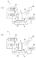
図1(a)において、本発明に係る半導体ウェハ荷電キャリア寿命測定装置の第1実施形態である荷電キャリア寿命測定装置2は、半導体ウェハ10の下面8を保持する導電性チャック4と、弾性変形可能な導電性測定プローブ6とを備える。
測定プローブとしては、弾性変形可能かつ導電性を有するもの、例えばタンタル等の金属に化学的にエッチング処理を施したものを用いることができる。
プローブ6の先端部12には、半導体ウェハ10の上面14に接触する球状面が形成される。但し、プローブ6の先端部12は任意の形状とすることができるため、本発明は上記形状に限られるものではない。
チャック4及び/またはプローブ6には移動手段20が接続され、プローブ6の先端部12と半導体ウェハ10の上面14とを相対移動させることで両者を接触させる。
Referring to FIG. 1A, a charge carrier
As the measurement probe, a probe having elastic conductivity and conductivity, for example, a probe obtained by chemically etching a metal such as tantalum can be used.
A spherical surface that contacts the
The moving
チャック4とプローブ6とを接続するように電気的刺激付与手段22が設けられ、半導体ウェハ10がチャック4に保持されかつプローブ6の先端部12が半導体ウェハ10の上面14に接触しているとき、半導体ウェハ10に試験用の電気的刺激を付与する。
試験用電気的刺激としては、例えば、図2に示されるような静電容量−電圧(CV)型の電気的刺激24がある。電気的刺激24は交流電圧(図示せず)が重畳された直流電圧であり、半導体ウェハ10の閾値電圧(VT)28よりも小さい第1の電圧値(VSTART)26から、閾値電圧28よりも大きい第2の電圧値(VMEAS)30まで変化する。
Electrical stimulating means 22 is provided so as to connect the chuck 4 and the
As the test electrical stimulus, for example, there is a capacitance-voltage (CV) type
直流電圧をゆっくりと変化させることで、半導体層18におけるプローブ6との接触点の下方に位置する箇所に少数キャリアを発生させる。
本実施形態で用いるCV型の電気的刺激24は、半導体ウェハ10がp型シリコンから形成される場合に用いるものである。半導体ウェハ10がn型シリコンから形成される場合にはCV型の電気的刺激24を反転させればよい。
By slowly changing the DC voltage, minority carriers are generated in a portion of the
The CV type
測定装置2にはキセノンランプなどの光源34を設け、この光源34からプローブ6との接触点付近にある半導体ウェハ10に対して光パルス36を照射する。
チャック4とプローブ6との間には測定手段38が接続され、光パルス36に対する半導体ウェハ10の反応を測定し、この測定値から半導体ウェハ10の荷電キャリア寿命を測定する。
The
Measuring means 38 is connected between the chuck 4 and the
図1(a)に示される半導体ウェハ10は、半導体層18と、この半導体層を覆う誘電層16とを有する。このため、本実施形態において、半導体ウェハ10の上面14は、半導体層18の反対側に位置する誘電層の面を指す。
The
図1(b)には、本発明に係る半導体ウェハ荷電キャリア寿命測定装置の第2実施形態である荷電キャリア寿命測定装置2’が示される。測定装置2’には、弾性変形可能な導電性プローブ6’が設けられ、このプローブには先端部12’と、少なくとも先端部12’を覆う誘電層16’とが形成される。
FIG. 1B shows a charged carrier
導電性プローブ6’に誘電層16’を形成することで、半導体ウェハ10’の半導体層18に対して直接電気測定を行うことができるようになる。即ち、半導体層18を覆う誘電層を半導体ウェハ10’に形成しなくても、先端部12’を覆う誘電層16’が形成されたプローブ6’は、半導体層18の上面14’に直接接触可能となる。
By forming the dielectric layer 16 'on the' conductive probe 6 ', electrical measurements can be directly performed on the
プローブ6’の材料としては、弾性変形可能かつ導電性を有するもの、例えばタンタルを用いることができる。プローブ6の少なくとも先端部12にタンタルを用いた場合、先端部12の外面には外気への露出に伴って自生の酸化層が成長する。この酸化層が誘電層16’となる。また、プローブ6’をタンタル製としつつ、誘電層16’は熱により成長した金属酸化物とすることもできる。
但し、誘電層16’は、少なくとも先端部12’付近のプローブ6’の外面で成長するまたは同外面に塗布されかつ高誘電率を有するものであればいかなる材料でもよい。
ここで、誘電率は3.9以上であることが好ましい。
成長した誘電層としては、例えば酸化タンタルがあり、塗布された誘電層16’としては例えばシリコンゴムがある。
As a material of the probe 6 ', a material having elasticity and conductivity and, for example, tantalum can be used. When tantalum is used for at least the
However, the dielectric layer 16 'may be made of any material as long as it grows at least on the outer surface of the probe 6' near the distal end 12 'or is coated on the outer surface and has a high dielectric constant.
Here, the dielectric constant is preferably 3.9 or more.
The grown dielectric layer is, for example, tantalum oxide, and the applied dielectric layer 16 'is, for example, silicon rubber.
図1(a)に示す測定装置2では、プローブ6の先端部12と半導体ウェハ10の上面14とが接触することでキャパシタを形成する。即ち、プローブ6がキャパシタの第1のプレートとなり、半導体層18がキャパシタの第2のプレートとなり、誘電層16が両者の間に配置された絶縁体となる。
(1) In the
同様に、図1(b)に示す測定装置2’では、プローブ6’の先端部12’と半導体ウェハ10’の上面14’とを接触させることでキャパシタを形成する。即ち、プローブ6’の導電部がキャパシタの第1のプレートとなり、半導体層18がキャパシタの第2のプレートとなり、誘電層16’が両者の間に配置された絶縁体となる。
Similarly, in the measuring device 2 'shown in FIG. 1B, a capacitor is formed by bringing the tip 12' of the probe 6 'into contact with the upper surface 14' of the semiconductor wafer 10 '. That is, the conductive portion of the probe 6 'serves as the first plate of the capacitor, the
図1(a)に示す測定装置2を用いた測定方法では、半導体ウェハ10の下面8をチャック4に保持させた状態で、プローブ6の先端部12と半導体ウェハ10の上面14とを相対移動させて両者を接触させる。
その後、電気的刺激付与手段22を用いて、プローブ6とチャック4との間にCV型の電気的刺激24を付与する。より具体的には、電気的刺激付与手段22により、交流電圧を重畳した直流電圧を第1の電圧値26と第2の電圧値30との間で変化させる。
In the measuring method using the
After that, the CV-type
CV型の電気的刺激24を付与する間、測定手段38により、プローブ6及び半導体ウェハ10から形成されたキャパシタにおける静電容量の変化を、第1の電圧値26における最大静電容量値(Cmax)40から第2の電圧値30における最小静電容量(Cmin)42まで計測する。
During the application of the CV-type
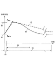
CV型の電気的刺激が第2の電圧値30になったとき、光源34から光パルス36を照射する。照射された光パルス36は、半導体層18のうちプローブ6との接触点下方に位置する箇所で吸収される。この吸収は光電効果による電子と正孔の対の発生に伴って起こるものであり、これにより、プローブ6と半導体ウェハ10から形成されたキャパシタの静電容量は、図2の矢印44で示すように増加する。
When the CV-type electrical stimulus reaches the
光パルス36の強度は、測定手段38が測定する静電容量が最大静電容量値40に到達するのに十分であることが好ましいがこれに限られるものではない。
光パルス36の照射が終了すると、プローブ6及び半導体ウェハ10からなるキャパシタの静電容量は、図2の矢印46で示すように、最大静電容量値40から最小静電容量値42へと減少する。
The intensity of the
When the irradiation of the
図3において、光パルス36を所定の照射時間50の間照射させると、プローブ6及び半導体ウェハ10からなるキャパシタの静電容量は、最小静電容量値42から最大静電容量値40へと増加する。
照射時間50が経過し、光パルス36の照射を終了させると、光パルス36と半導体ウェハ10の半導体層18との相互作用に対応して発生した電子・正孔の対が再結合を開始するとともに、プローブ6及び半導体ウェハ10からなるキャパシタの静電容量は所定時間52の間に最大静電容量値40から最小静電容量値42に向かって減少し始める。
In FIG. 3, when the
When the irradiation of the
再結合の割合、即ち、静電容量の減少は、半導体ウェハ18の欠陥及び不純物濃度に大きく依存する。測定手段38はキャパシタの静電容量の変化を時間ごとに測定し、この結果に基づき、半導体ウェハ10の荷電キャリア寿命を測定する。
より具体的には、測定手段38は、キャパシタにおける静電容量の時間変化率を測定し、この結果に基づき、半導体ウェハ10の荷電キャリア寿命を測定する。
The rate of recombination, that is, the decrease in capacitance, largely depends on the defect and impurity concentration of the
More specifically, the measuring
光電効果により発生した電子・正孔の対の再結合率は光パルス36の照射終了直後に最大となるため、キャパシタにおける静電容量の時間変化率は、光パルス36の照射終了直後の短時間に測定する。
このため、キャパシタにおける静電容量の時間変化率は、光パルス36の照射終了後から所定時間54を経た時点で測定される。所定時間54を経た時点でのキャパシタにおける静電容量の時間変化率は、半導体層18の欠陥及び不純物濃度に関連付けることができる。
Since the recombination rate of the electron-hole pair generated by the photoelectric effect becomes maximum immediately after the end of the irradiation of the
Therefore, the time rate of change of the capacitance of the capacitor is measured at a point in time when a
複数の半導体ウェハ10に形成されたキャパシタにおける静電容量の時間変化率の測定は、光パルス36の照射終了時点から略同一の時点で行うことにより、複数の半導体ウェハ10間で半導体層の欠陥及び不純度濃度を関連付けることが好ましい。しかし、本発明はこの構成に限られるものではない。
The measurement of the time rate of change of the capacitance of the capacitors formed on the plurality of
図3において、実線60は不純物濃度の高い半導体層18に関する時間ごとの静電容量の変化を示し、破線62は不純物濃度の低い半導体層18に関する時間ごとの静電容量の変化を示す。
図示されるように、所定時間54を経た時点における実線60の時間変化率は破線62の時間変化率よりも大きい。即ち、不純物濃度の高い半導体層18に関する実線60は、不純物濃度の低い半導体層18に関する破線62よりも傾斜が大きい。実線60及び破線62における傾斜の相違は、2枚の半導体ウェハ10の荷電キャリア寿命に関連付けることができる。
In FIG. 3, a
As illustrated, the time change rate of the
上記測定方法は図1(a)に示した第1実施形態の測定装置2を参照して説明したが、当業者にとって、図1(b)に示した第2実施形態の測定装置2’でも同様に利用可能であることは自明であろう。従って、不必要な繰返しを避けるため、図1(b)に示す測定装置2’に関する詳細説明は省略する。
Although the above measuring method has been described with reference to the
以上のように、本発明では、半導体ウェハの荷電キャリア寿命の測定方法及び測定装置を提供できる。また、本発明の測定装置及び測定方法は非破壊式であるため、製品用半導体ウェハにも用いることができる。 As described above, the present invention can provide a method and an apparatus for measuring the charge carrier life of a semiconductor wafer. Further, since the measuring device and the measuring method of the present invention are non-destructive, they can be used for semiconductor wafers for products.
好適な実施形態を参照して本発明を説明してきた。上記説明を読みこれを理解したとき、その他の変形や変更も明らかになるであろう。
例えば、前記実施形態ではp型シリコンからなる半導体ウェハ10に対してCV型の電気的刺激24を用いたが、これに限られず、CV型の電気的刺激24を反転させてn型シリコンからなる半導体ウェハ10に用いることもできる。
また、前記実施形態では、半導体ウェハの面として上面14、14’と下面8を示したが、これに限られず、電気的刺激24の付与により、時間ごとの静電容量の変化を測定可能であればどのような位置関係でもよい。
The invention has been described with reference to the preferred embodiment. Other variations and modifications will become apparent upon reading and understanding the above description.
For example, in the above-described embodiment, the CV-type
In the above-described embodiment, the
前記第1実施形態では、プローブ6は誘電層を備えないものとしたが、備えるもの(例えば、第2実施形態のプローブ6’と同様の構成)であってもよい。即ち、プローブ6をキャパシタの第1のプレートとし、半導体層18を第2のプレートとし、プローブ6の誘電層及び半導体ウェハ10の誘電層16を誘電層とする構成とすることも可能である。この場合、プローブ6の誘電層が加わる分キャパシタンスがより大きくなり、この結果、インピーダンスがより小さくなる。ここで、プローブ6の誘電層のキャパシタンスを事前に測定しておき、これを実際のデータに反映させる処理を加えることもできるが、そのような処理なしに静電容量の時間変化率を比較することも可能である。
本発明は、説明の範囲内にある変形や変更はすべて含むものと理解されたい。
In the first embodiment, the
It is to be understood that the invention includes all modifications and changes that fall within the scope of the description.
2、2’ 荷電キャリア寿命測定装置
4 ウェハ保持手段であるチャック
6、6’ 測定プローブ
8 半導体ウェハの下面
10、10’ 半導体ウェハ
12 測定プローブの先端部
14 半導体ウェハの上面
16 半導体ウェハの誘電層
16’ 測定プローブの誘電層
18 半導体ウェハの半導体層
20 移動手段
22 電気的刺激付与手段
24 電気的刺激(直流電圧)
26 第1の電圧値
28 閾値電圧
30 第2の電圧値
34 光源
36 光パルス
38 測定手段
40 キャパシタの最大静電容量値
42 キャパシタの最小静電容量値
2, 2 'Charge carrier lifetime measuring device 4 Wafer holding means 6, 6'
26
Claims (20)
(a)導電性測定プローブと半導体ウェハの表面とを接触させてキャパシタを形成するキャパシタ形成工程と、
(b)交流電圧を重畳した直流電圧を、前記測定プローブと前記半導体ウェハの間に付与する電圧付与工程と、
(c)前記直流電圧を第1の電圧値と第2の電圧値との間で変化させる電圧変化工程と、
(d)前記半導体ウェハにおける前記測定プローブとの接触点近傍の箇所に光パルスを照射する光パルス照射工程と、
(e)前記キャパシタにおける静電容量の時間ごとの変化を前記光パルスの照射終了後に測定する静電容量変化測定工程と、
(f)前記測定した静電容量の変化に基づき、前記半導体ウェハの荷電キャリア寿命を測定する荷電キャリア寿命測定工程と、を備えることを特徴とする荷電キャリア寿命測定方法。 A method for measuring a charge carrier life of a semiconductor wafer,
(A) a capacitor forming step of forming a capacitor by bringing a conductivity measurement probe into contact with a surface of a semiconductor wafer;
(B) a voltage application step of applying a DC voltage on which an AC voltage is superimposed between the measurement probe and the semiconductor wafer;
(C) a voltage changing step of changing the DC voltage between a first voltage value and a second voltage value;
(D) an optical pulse irradiating step of irradiating an optical pulse to a portion of the semiconductor wafer near a contact point with the measurement probe;
(E) a capacitance change measuring step of measuring a time-dependent change in capacitance of the capacitor after the end of the light pulse irradiation;
(F) a charged carrier life measuring step of measuring a charged carrier life of the semiconductor wafer based on the measured change in capacitance.
前記半導体ウェハは、半導体層と、この半導体層を覆う誘電層とを備え、
前記測定プローブが前記誘電層に接触することで前記キャパシタを形成し、
前記キャパシタでは、前記測定プローブが第1プレートとなり、前記半導体層が第2プレートとなり、前記誘電層が前記両プレート間の絶縁体となることを特徴とする荷電キャリア寿命測定方法。 The charge carrier lifetime measuring method according to claim 1,
The semiconductor wafer includes a semiconductor layer and a dielectric layer covering the semiconductor layer,
The measurement probe contacts the dielectric layer to form the capacitor,
In the capacitor, the charge carrier lifetime measurement method is characterized in that the measurement probe serves as a first plate, the semiconductor layer serves as a second plate, and the dielectric layer serves as an insulator between the two plates.
前記測定プローブには前記半導体ウェハと接触する誘電層が形成され、
前記誘電層は、前記測定プローブの外面で成長するものまたは前記測定プローブの外面に塗布されるものであることを特徴とする荷電キャリア寿命測定方法。 The charge carrier lifetime measuring method according to claim 1,
The measurement probe is formed with a dielectric layer in contact with the semiconductor wafer,
The method of measuring a charge carrier lifetime, wherein the dielectric layer is grown on an outer surface of the measurement probe or is applied on an outer surface of the measurement probe.
前記測定プローブにおいて少なくとも前記半導体ウェハと接触する箇所は弾性変形可能な材料からなることを特徴とする荷電キャリア寿命測定方法。 The charged carrier lifetime measuring method according to any one of claims 1 to 3,
At least a portion of the measurement probe that contacts the semiconductor wafer is made of an elastically deformable material.
前記キャパシタは、前記第2の電圧値において最小静電容量値となり、
前記キャパシタの静電容量値は前記光パルスに対応して前記最小静電容量値から増加し、
前記光パルスの照射終了後、前記キャパシタの静電容量値は前記増加した静電容量値から前記最小静電容量値へと減少することを特徴とする荷電キャリア寿命測定方法。 The charged carrier life measuring method according to any one of claims 1 to 4,
The capacitor has a minimum capacitance value at the second voltage value,
A capacitance value of the capacitor increases from the minimum capacitance value in response to the light pulse;
After the irradiation of the light pulse is completed, the capacitance value of the capacitor decreases from the increased capacitance value to the minimum capacitance value.
前記静電容量変化測定工程では、前記キャパシタにおける静電容量の時間変化率を測定し、
前記荷電キャリア寿命測定工程では、前記キャパシタにおける静電容量の時間変化率に基づき、前記半導体ウェハの荷電キャリア寿命を測定することを特徴とする荷電キャリア寿命測定方法。 The method for measuring the life of a charged carrier according to any one of claims 1 to 5,
In the capacitance change measurement step, a time change rate of the capacitance of the capacitor is measured,
In the charged carrier life measuring step, a charged carrier life measuring method is characterized in that a charged carrier life of the semiconductor wafer is measured based on a time change rate of a capacitance of the capacitor.
前記キャパシタにおける静電容量の時間変化率は、前記光パルスの照射終了直後の短時間に測定されることを特徴とする荷電キャリア寿命測定方法。 The method for measuring the life of a charged carrier according to claim 6,
The charge carrier lifetime measurement method according to claim 1, wherein the time change rate of the capacitance of the capacitor is measured in a short time immediately after the end of the light pulse irradiation.
前記光パルス照射工程及び前記静電容量変化測定工程は、前記直流電圧が前記第2の電圧値であるときに行われることを特徴とする荷電キャリア寿命測定方法。 The charged carrier life measuring method according to any one of claims 1 to 7,
The method for measuring the life of a charged carrier, wherein the light pulse irradiation step and the capacitance change measurement step are performed when the DC voltage is the second voltage value.
半導体ウェハの第1の面を保持する導電性ウェハ保持手段と、
導電性測定プローブと、
前記ウェハ保持手段が前記半導体ウェハを保持した状態で、前記測定プローブ及び前記半導体ウェハの第2の面を相対移動させて両者を接触させることでキャパシタを形成させる移動手段と、
交流電圧が重畳された直流電圧を前記キャパシタに付与し、前記直流電圧を第1の電圧値から第2の電圧値に変化させる電気的刺激付与手段と、
前記半導体ウェハにおける前記測定プローブとの接触点近傍の箇所に光パルスを照射する光源と、
前記光パルスの照射終了後に前記キャパシタにおける静電容量の変化を時間ごとに測定し、この時間ごとの静電容量の変化に基づいて、前記半導体ウェハの荷電キャリア寿命を測定する測定手段と、を備えることを特徴とする荷電キャリア寿命測定装置。 A charge carrier life measuring device for a semiconductor wafer,
Conductive wafer holding means for holding a first surface of a semiconductor wafer;
A conductivity measuring probe;
Moving means for forming a capacitor by relatively moving the measurement probe and the second surface of the semiconductor wafer and bringing them into contact with each other while the wafer holding means holds the semiconductor wafer;
An electrical stimulus applying unit that applies a DC voltage on which an AC voltage is superimposed to the capacitor, and changes the DC voltage from a first voltage value to a second voltage value;
A light source that irradiates a light pulse to a location near a contact point with the measurement probe on the semiconductor wafer,
Measuring the change in capacitance of the capacitor at each time after the irradiation of the light pulse, and measuring the charge carrier life of the semiconductor wafer based on the change of capacitance at each time, A charge carrier lifetime measuring device, comprising:
前記測定プローブと前記半導体ウェハとの接触は、前記測定プローブと、前記半導体ウェハの半導体層を覆う誘電層との間で行われることを特徴とする荷電キャリア寿命測定装置。 The charge carrier life measuring device according to claim 9,
The charged carrier life measuring apparatus according to claim 1, wherein the contact between the measurement probe and the semiconductor wafer is performed between the measurement probe and a dielectric layer covering a semiconductor layer of the semiconductor wafer.
前記測定プローブには、前記半導体ウェハと接触する誘電層が形成され、
前記誘電層は、前記測定プローブの外面で成長するものまたは前記測定プローブ外面に塗布されるものであることを特徴とする荷電キャリア寿命測定装置。 The charge carrier life measuring device according to claim 9,
The measurement probe is formed with a dielectric layer in contact with the semiconductor wafer,
The charge carrier lifetime measuring device according to claim 1, wherein the dielectric layer is grown on an outer surface of the measurement probe or is applied to an outer surface of the measurement probe.
前記測定プローブにおいて少なくとも前記半導体ウェハと接触する箇所は弾性変形可能な材料からなることを特徴とする荷電キャリア寿命測定装置。 The charged carrier life measuring device according to any one of claims 9 to 11,
At least a portion of the measurement probe that comes into contact with the semiconductor wafer is made of an elastically deformable material.
前記キャパシタは、前記第2の電圧値において最小静電容量値となり、
前記キャパシタの静電容量値は前記光パルスに対応して増加し、
前記測定手段は、前記増加した静電容量値から前記最小静電容量値への静電容量値の変化を時間ごとに測定することを特徴とする荷電キャリア測定装置。 The charged carrier life measuring device according to any one of claims 9 to 12,
The capacitor has a minimum capacitance value at the second voltage value,
The capacitance value of the capacitor increases in response to the light pulse,
The charge carrier measuring device according to claim 1, wherein the measuring unit measures a change in the capacitance value from the increased capacitance value to the minimum capacitance value every time.
前記測定手段は、前記キャパシタにおける静電容量の時間変化率を測定し、この時間変化率に基づき、前記半導体ウェハの荷電キャリア寿命を測定することを特徴とする荷電キャリア寿命測定装置。 The charged carrier life measuring device according to any one of claims 9 to 13,
The charge carrier life measuring device, wherein the measuring means measures a time change rate of the capacitance of the capacitor, and measures a charge carrier life of the semiconductor wafer based on the time change rate.
前記光源による光パルスの照射及び前記測定手段による前記時間ごとの静電容量の変化の測定は、前記直流電圧が前記第2の電圧値であるときになされることを特徴とする荷電キャリア寿命測定装置。 The charged carrier life measuring device according to any one of claims 9 to 14,
The charge carrier lifetime measurement, wherein the irradiation of the light pulse by the light source and the measurement of the change of the capacitance every time by the measuring means are performed when the DC voltage is the second voltage value. apparatus.
(a)半導体ウェハの表面を用いてキャパシタを形成するキャパシタ形成工程と、
(b)前記キャパシタに付与する試験用電圧を第1の電圧値から第2の電圧値へと変化させる電圧変化工程と、
(c)前記半導体ウェハに光パルスを照射して前記キャパシタにおける静電容量を増加させる光パルス照射工程と、
(d)前記キャパシタの静電容量が減少する時間変化率を測定する時間変化率測定工程と、
(e)前記測定した時間変化率に基づき、前記半導体ウェハの荷電キャリア寿命を測定する荷電キャリア寿命測定工程と、を備えることを特徴とする荷電キャリア寿命測定方法。 A method for measuring a charge carrier life of a semiconductor wafer,
(A) a capacitor forming step of forming a capacitor using a surface of a semiconductor wafer;
(B) a voltage changing step of changing a test voltage applied to the capacitor from a first voltage value to a second voltage value;
(C) a light pulse irradiation step of irradiating the semiconductor wafer with a light pulse to increase the capacitance of the capacitor;
(D) a time change rate measuring step of measuring a time change rate at which the capacitance of the capacitor decreases;
(E) a charged carrier life measuring step of measuring a charged carrier life of the semiconductor wafer based on the measured rate of change in time.
前記時間変化率測定工程は、前記光パルスの照射終了後に行われることを特徴とする荷電キャリア寿命測定方法。 The charge carrier lifetime measuring method according to claim 16,
The method of measuring a charge carrier lifetime, wherein the time change rate measuring step is performed after the irradiation of the light pulse is completed.
前記キャパシタ形成工程では、導電性測定プローブと前記半導体ウェハの半導体層との間に誘電層を挟むことを特徴とする荷電キャリア寿命測定方法。 In the charge carrier lifetime measuring method according to claim 16 or claim 17,
In the capacitor forming step, a charge carrier lifetime measuring method, wherein a dielectric layer is interposed between a conductivity measuring probe and a semiconductor layer of the semiconductor wafer.
前記誘電層は、前記半導体層を覆う誘電層、前記測定プローブの外面で成長する誘電層、前記測定プローブの外面に塗布された誘電層のいずれかであることを特徴とする荷電キャリア寿命測定方法。 In the charge carrier life measuring method according to claim 18,
The charge carrier lifetime measuring method, wherein the dielectric layer is any one of a dielectric layer covering the semiconductor layer, a dielectric layer grown on an outer surface of the measurement probe, and a dielectric layer applied to an outer surface of the measurement probe. .
前記キャパシタにおける静電容量の時間変化率は、前記光パルスの照射終了直後の短時間に測定されることを特徴とする荷電キャリア寿命測定方法。
The charged carrier life measuring method according to any one of claims 16 to 19,
The charge carrier lifetime measurement method according to claim 1, wherein the time change rate of the capacitance of the capacitor is measured in a short time immediately after the end of the light pulse irradiation.
Applications Claiming Priority (1)
| Application Number | Priority Date | Filing Date | Title |
|---|---|---|---|
| US10/277,689 US6836139B2 (en) | 2002-10-22 | 2002-10-22 | Method and apparatus for determining defect and impurity concentration in semiconducting material of a semiconductor wafer |
Publications (1)
| Publication Number | Publication Date |
|---|---|
| JP2004146831A true JP2004146831A (en) | 2004-05-20 |
Family
ID=32069312
Family Applications (1)
| Application Number | Title | Priority Date | Filing Date |
|---|---|---|---|
| JP2003360629A Pending JP2004146831A (en) | 2002-10-22 | 2003-10-21 | Method for measuring electrical charge carrier lifetime of semiconductor wafer and its measurement apparatus |
Country Status (6)
| Country | Link |
|---|---|
| US (1) | US6836139B2 (en) |
| EP (1) | EP1413892B1 (en) |
| JP (1) | JP2004146831A (en) |
| AT (1) | ATE399329T1 (en) |
| DE (1) | DE60321761D1 (en) |
| TW (1) | TWI296329B (en) |
Cited By (1)
| Publication number | Priority date | Publication date | Assignee | Title |
|---|---|---|---|---|
| KR101483716B1 (en) * | 2013-12-27 | 2015-01-16 | 국민대학교산학협력단 | Method for extracting excess carrier lifetimes of organic thin-film transistor using optical response characteristic, and apparatus thereof |
Families Citing this family (10)
| Publication number | Priority date | Publication date | Assignee | Title |
|---|---|---|---|---|
| AU2003279929A1 (en) * | 2003-01-28 | 2004-08-30 | The Government Of The United States Of America As Represented By The Secretary Of Commerce | Light-induced capacitance spectroscopy and method for obtaining carrier lifetime with micron/nanometer scale |
| US7023231B2 (en) * | 2004-05-14 | 2006-04-04 | Solid State Measurements, Inc. | Work function controlled probe for measuring properties of a semiconductor wafer and method of use thereof |
| US7037734B2 (en) * | 2004-06-23 | 2006-05-02 | Solid State Measurements, Inc. | Method and apparatus for determining generation lifetime of product semiconductor wafers |
| DE102006013588A1 (en) * | 2006-03-22 | 2007-09-27 | Fachhochschule Deggendorf | Two-dimensional profiling of doping profiles of a material sample by scanning probe microscopy |
| WO2008052237A1 (en) * | 2006-10-30 | 2008-05-08 | Newsouth Innovations Pty Limited | Methods and systems of producing self-consistently a calibration constant for excess charge carrier lifetime |
| KR101913311B1 (en) * | 2012-04-09 | 2019-01-15 | 삼성디스플레이 주식회사 | Method of measuring a silicon thin film, method of detecting defects in a silicon thin film, and apparatus for detecting defects in a silicon thin film |
| TWI555326B (en) * | 2015-05-29 | 2016-10-21 | Lehighton Electronics Inc | System and method for noncontact sensing maximum open circuit voltage of photovoltaic semiconductors |
| CN111398774B (en) * | 2020-03-18 | 2022-02-15 | 西安奕斯伟材料科技有限公司 | Method and device for testing minority carrier lifetime of silicon wafer |
| RU2750427C1 (en) * | 2020-10-20 | 2021-06-28 | Федеральное государственное бюджетное образовательное учреждение высшего образования "Тверской государственный университет" | Method for determining the electrical resistivity of semiconductors using infrared optics |
| US11940489B2 (en) * | 2021-10-15 | 2024-03-26 | Infineon Technologies Ag | Semiconductor device having an optical device degradation sensor |
Citations (3)
| Publication number | Priority date | Publication date | Assignee | Title |
|---|---|---|---|---|
| JPH0252342U (en) * | 1988-09-30 | 1990-04-16 | ||
| JPH11186350A (en) * | 1997-12-16 | 1999-07-09 | Dainippon Screen Mfg Co Ltd | Recombination life time measuring method for minority carriers of semiconductor |
| WO2002077654A1 (en) * | 2001-03-23 | 2002-10-03 | Solid State Measurements, Inc. | Method of detecting carrier dose of a semiconductor wafer |
Family Cites Families (29)
| Publication number | Priority date | Publication date | Assignee | Title |
|---|---|---|---|---|
| US4168212A (en) * | 1974-05-16 | 1979-09-18 | The Post Office | Determining semiconductor characteristic |
| JPS59141238A (en) * | 1983-02-01 | 1984-08-13 | Hitachi Ltd | Carrier life measuring device |
| US5065103A (en) * | 1990-03-27 | 1991-11-12 | International Business Machines Corporation | Scanning capacitance - voltage microscopy |
| US5406214A (en) * | 1990-12-17 | 1995-04-11 | Semilab Felvezeto Fizikai Lab, Rt | Method and apparatus for measuring minority carrier lifetime in semiconductor materials |
| JPH06151538A (en) * | 1992-02-03 | 1994-05-31 | Leo Giken:Kk | Method and apparatus for evaluation of semiconductor wafer |
| US5508610A (en) * | 1992-12-03 | 1996-04-16 | Georgia Tech Research Corporation | Electrical conductivity tester and methods thereof for accurately measuring time-varying and steady state conductivity using phase shift detection |
| US5477158A (en) * | 1993-10-04 | 1995-12-19 | Loral Vought Systems Corporation | Compact noncontact excess carrier lifetime characterization apparatus |
| US5453703A (en) * | 1993-11-29 | 1995-09-26 | Semitest Inc. | Method for determining the minority carrier surface recombination lifetime constant (ts of a specimen of semiconductor material |
| US5500607A (en) * | 1993-12-22 | 1996-03-19 | International Business Machines Corporation | Probe-oxide-semiconductor method and apparatus for measuring oxide charge on a semiconductor wafer |
| US5667300A (en) * | 1994-06-22 | 1997-09-16 | Mandelis; Andreas | Non-contact photothermal method for measuring thermal diffusivity and electronic defect properties of solids |
| DE4432294A1 (en) | 1994-09-12 | 1996-03-14 | Telefunken Microelectron | Process for reducing the surface recombination speed in silicon |
| US5663657A (en) * | 1994-09-26 | 1997-09-02 | University Of South Florida | Determining long minority carrier diffusion lengths |
| US5661408A (en) | 1995-03-01 | 1997-08-26 | Qc Solutions, Inc. | Real-time in-line testing of semiconductor wafers |
| TW341664B (en) * | 1995-05-12 | 1998-10-01 | Ibm | Photovoltaic oxide charge measurement probe technique |
| US6008906A (en) * | 1995-08-25 | 1999-12-28 | Brown University Research Foundation | Optical method for the characterization of the electrical properties of semiconductors and insulating films |
| US6011404A (en) * | 1997-07-03 | 2000-01-04 | Lucent Technologies Inc. | System and method for determining near--surface lifetimes and the tunneling field of a dielectric in a semiconductor |
| US5977788A (en) * | 1997-07-11 | 1999-11-02 | Lagowski; Jacek | Elevated temperature measurement of the minority carrier lifetime in the depletion layer of a semiconductor wafer |
| EP0898298B1 (en) * | 1997-07-15 | 2007-09-12 | STMicroelectronics S.r.l. | Determination of the thickness of a denuded zone in a silicon wafer |
| JP3568741B2 (en) * | 1997-07-31 | 2004-09-22 | 株式会社東芝 | Semiconductor evaluation device and semiconductor manufacturing system |
| US6005400A (en) * | 1997-08-22 | 1999-12-21 | Lockheed Martin Energy Research Corporation | High resolution three-dimensional doping profiler |
| US6369603B1 (en) | 1997-09-02 | 2002-04-09 | Midwest Research Institute | Radio frequency coupling apparatus and method for measuring minority carrier lifetimes in semiconductor materials |
| US6275060B1 (en) | 1997-09-02 | 2001-08-14 | Midwest Research Institute | Apparatus and method for measuring minority carrier lifetimes in semiconductor materials |
| US6185991B1 (en) * | 1998-02-17 | 2001-02-13 | Psia Corporation | Method and apparatus for measuring mechanical and electrical characteristics of a surface using electrostatic force modulation microscopy which operates in contact mode |
| US6346821B1 (en) | 1998-03-27 | 2002-02-12 | Infineon Technologies Ag | Method for nondestructive measurement of minority carrier diffusion length and minority carrier lifetime in semiconductor devices |
| US6049220A (en) * | 1998-06-10 | 2000-04-11 | Boxer Cross Incorporated | Apparatus and method for evaluating a wafer of semiconductor material |
| JP3235573B2 (en) | 1998-11-05 | 2001-12-04 | 日本電気株式会社 | Semiconductor device test system |
| US6150175A (en) * | 1998-12-15 | 2000-11-21 | Lsi Logic Corporation | Copper contamination control of in-line probe instruments |
| US6323951B1 (en) | 1999-03-22 | 2001-11-27 | Boxer Cross Incorporated | Apparatus and method for determining the active dopant profile in a semiconductor wafer |
| DE19915051C2 (en) * | 1999-04-01 | 2002-09-19 | Zae Bayern | Method and device for the spatially resolved characterization of electronic properties of semiconductor materials |
-
2002
- 2002-10-22 US US10/277,689 patent/US6836139B2/en not_active Expired - Fee Related
-
2003
- 2003-10-15 TW TW092128634A patent/TWI296329B/en not_active IP Right Cessation
- 2003-10-21 JP JP2003360629A patent/JP2004146831A/en active Pending
- 2003-10-22 EP EP03078341A patent/EP1413892B1/en not_active Expired - Lifetime
- 2003-10-22 AT AT03078341T patent/ATE399329T1/en not_active IP Right Cessation
- 2003-10-22 DE DE60321761T patent/DE60321761D1/en not_active Expired - Fee Related
Patent Citations (3)
| Publication number | Priority date | Publication date | Assignee | Title |
|---|---|---|---|---|
| JPH0252342U (en) * | 1988-09-30 | 1990-04-16 | ||
| JPH11186350A (en) * | 1997-12-16 | 1999-07-09 | Dainippon Screen Mfg Co Ltd | Recombination life time measuring method for minority carriers of semiconductor |
| WO2002077654A1 (en) * | 2001-03-23 | 2002-10-03 | Solid State Measurements, Inc. | Method of detecting carrier dose of a semiconductor wafer |
Cited By (1)
| Publication number | Priority date | Publication date | Assignee | Title |
|---|---|---|---|---|
| KR101483716B1 (en) * | 2013-12-27 | 2015-01-16 | 국민대학교산학협력단 | Method for extracting excess carrier lifetimes of organic thin-film transistor using optical response characteristic, and apparatus thereof |
Also Published As
| Publication number | Publication date |
|---|---|
| DE60321761D1 (en) | 2008-08-07 |
| EP1413892A2 (en) | 2004-04-28 |
| EP1413892A3 (en) | 2005-01-12 |
| TW200413735A (en) | 2004-08-01 |
| US6836139B2 (en) | 2004-12-28 |
| US20040075460A1 (en) | 2004-04-22 |
| ATE399329T1 (en) | 2008-07-15 |
| TWI296329B (en) | 2008-05-01 |
| EP1413892B1 (en) | 2008-06-25 |
Similar Documents
| Publication | Publication Date | Title |
|---|---|---|
| KR101101132B1 (en) | LED inspection apparatus and inspection method using the same | |
| US6538462B1 (en) | Method for measuring stress induced leakage current and gate dielectric integrity using corona discharge | |
| US4758786A (en) | Method of analyzing semiconductor systems | |
| JP2004146831A (en) | Method for measuring electrical charge carrier lifetime of semiconductor wafer and its measurement apparatus | |
| JP2005333148A (en) | Probe where work function to measure characteristics of semiconductor wafer is controlled and using method of the same | |
| JP2005045216A (en) | Flexible membrane probe and method to use it | |
| JP2005517188A5 (en) | ||
| DE60029483D1 (en) | NON-INVASIVE ELECTRIC MEASUREMENT OF SEMICONDUCTOR DISCS | |
| US20150061715A1 (en) | Method and Apparatus for Non-Contact Measurement of Forward Voltage, Saturation Current Density, Ideality Factor and I-V Curves in P-N Junctions | |
| US6911350B2 (en) | Real-time in-line testing of semiconductor wafers | |
| JP2008515226A (en) | Method and apparatus for measuring the density of defects and / or impurities in a semiconductor wafer | |
| JP2005183933A (en) | Method of electrical characterization of silicon on insulator (soi) wafer | |
| JP4729246B2 (en) | High speed measurement method for threshold voltage and dopant concentration | |
| JP2006013532A (en) | Apparatus and method for detecting soft breakdown of dielectric layer of semiconductor wafer | |
| JP3736749B2 (en) | Method for measuring resistivity of semiconductor wafer | |
| JP2006013508A (en) | Method and device of determining lifetime of product semiconductor wafer | |
| JP2006295200A (en) | Method of measuring semiconductor wafer by oxide reinforcement probe | |
| JP2007220944A (en) | Evaluation method of semiconductor wafer | |
| KR0144253B1 (en) | Detecting method of mobile ion | |
| JP2004349342A (en) | Method for measuring capacitance of depletion layer | |
| JP2005277376A (en) | Method for determining leakage current of dielectric based on conductance-voltage(gv) | |
| JP2001351957A (en) | Method and apparatus for measuring by scanning electrostatic capacity microscope | |
| KR20110099200A (en) | Led inspection apparatus and inspection method using the same | |
| JP2000138266A (en) | Method for measuring electrical characteristics of semiconductor wafer | |
| KR20040098959A (en) | Metal impurities analysis apparatus of wafer |
Legal Events
| Date | Code | Title | Description |
|---|---|---|---|
| A621 | Written request for application examination |
Free format text: JAPANESE INTERMEDIATE CODE: A621 Effective date: 20060920 |
|
| A977 | Report on retrieval |
Free format text: JAPANESE INTERMEDIATE CODE: A971007 Effective date: 20091014 |
|
| A131 | Notification of reasons for refusal |
Free format text: JAPANESE INTERMEDIATE CODE: A131 Effective date: 20091027 |
|
| A02 | Decision of refusal |
Free format text: JAPANESE INTERMEDIATE CODE: A02 Effective date: 20100323 |