JP2004146785A - Component mounting method and component mounting device - Google Patents
Component mounting method and component mounting device Download PDFInfo
- Publication number
- JP2004146785A JP2004146785A JP2003197179A JP2003197179A JP2004146785A JP 2004146785 A JP2004146785 A JP 2004146785A JP 2003197179 A JP2003197179 A JP 2003197179A JP 2003197179 A JP2003197179 A JP 2003197179A JP 2004146785 A JP2004146785 A JP 2004146785A
- Authority
- JP
- Japan
- Prior art keywords
- component
- stage
- optical system
- suction head
- head
- Prior art date
- Legal status (The legal status is an assumption and is not a legal conclusion. Google has not performed a legal analysis and makes no representation as to the accuracy of the status listed.)
- Granted
Links
Images


Classifications
-
- H—ELECTRICITY
- H05—ELECTRIC TECHNIQUES NOT OTHERWISE PROVIDED FOR
- H05K—PRINTED CIRCUITS; CASINGS OR CONSTRUCTIONAL DETAILS OF ELECTRIC APPARATUS; MANUFACTURE OF ASSEMBLAGES OF ELECTRICAL COMPONENTS
- H05K13/00—Apparatus or processes specially adapted for manufacturing or adjusting assemblages of electric components
- H05K13/08—Monitoring manufacture of assemblages
- H05K13/081—Integration of optical monitoring devices in assembly lines; Processes using optical monitoring devices specially adapted for controlling devices or machines in assembly lines
- H05K13/0812—Integration of optical monitoring devices in assembly lines; Processes using optical monitoring devices specially adapted for controlling devices or machines in assembly lines the monitoring devices being integrated in the mounting machine, e.g. for monitoring components, leads, component placement
-
- Y—GENERAL TAGGING OF NEW TECHNOLOGICAL DEVELOPMENTS; GENERAL TAGGING OF CROSS-SECTIONAL TECHNOLOGIES SPANNING OVER SEVERAL SECTIONS OF THE IPC; TECHNICAL SUBJECTS COVERED BY FORMER USPC CROSS-REFERENCE ART COLLECTIONS [XRACs] AND DIGESTS
- Y10—TECHNICAL SUBJECTS COVERED BY FORMER USPC
- Y10T—TECHNICAL SUBJECTS COVERED BY FORMER US CLASSIFICATION
- Y10T29/00—Metal working
- Y10T29/49—Method of mechanical manufacture
- Y10T29/49002—Electrical device making
- Y10T29/49117—Conductor or circuit manufacturing
- Y10T29/49124—On flat or curved insulated base, e.g., printed circuit, etc.
- Y10T29/4913—Assembling to base an electrical component, e.g., capacitor, etc.
- Y10T29/49131—Assembling to base an electrical component, e.g., capacitor, etc. by utilizing optical sighting device
-
- Y—GENERAL TAGGING OF NEW TECHNOLOGICAL DEVELOPMENTS; GENERAL TAGGING OF CROSS-SECTIONAL TECHNOLOGIES SPANNING OVER SEVERAL SECTIONS OF THE IPC; TECHNICAL SUBJECTS COVERED BY FORMER USPC CROSS-REFERENCE ART COLLECTIONS [XRACs] AND DIGESTS
- Y10—TECHNICAL SUBJECTS COVERED BY FORMER USPC
- Y10T—TECHNICAL SUBJECTS COVERED BY FORMER US CLASSIFICATION
- Y10T29/00—Metal working
- Y10T29/49—Method of mechanical manufacture
- Y10T29/49002—Electrical device making
- Y10T29/49117—Conductor or circuit manufacturing
- Y10T29/49124—On flat or curved insulated base, e.g., printed circuit, etc.
- Y10T29/4913—Assembling to base an electrical component, e.g., capacitor, etc.
- Y10T29/49144—Assembling to base an electrical component, e.g., capacitor, etc. by metal fusion
-
- Y—GENERAL TAGGING OF NEW TECHNOLOGICAL DEVELOPMENTS; GENERAL TAGGING OF CROSS-SECTIONAL TECHNOLOGIES SPANNING OVER SEVERAL SECTIONS OF THE IPC; TECHNICAL SUBJECTS COVERED BY FORMER USPC CROSS-REFERENCE ART COLLECTIONS [XRACs] AND DIGESTS
- Y10—TECHNICAL SUBJECTS COVERED BY FORMER USPC
- Y10T—TECHNICAL SUBJECTS COVERED BY FORMER US CLASSIFICATION
- Y10T29/00—Metal working
- Y10T29/53—Means to assemble or disassemble
- Y10T29/5313—Means to assemble electrical device
- Y10T29/53174—Means to fasten electrical component to wiring board, base, or substrate
- Y10T29/53178—Chip component
-
- Y—GENERAL TAGGING OF NEW TECHNOLOGICAL DEVELOPMENTS; GENERAL TAGGING OF CROSS-SECTIONAL TECHNOLOGIES SPANNING OVER SEVERAL SECTIONS OF THE IPC; TECHNICAL SUBJECTS COVERED BY FORMER USPC CROSS-REFERENCE ART COLLECTIONS [XRACs] AND DIGESTS
- Y10—TECHNICAL SUBJECTS COVERED BY FORMER USPC
- Y10T—TECHNICAL SUBJECTS COVERED BY FORMER US CLASSIFICATION
- Y10T29/00—Metal working
- Y10T29/53—Means to assemble or disassemble
- Y10T29/5313—Means to assemble electrical device
- Y10T29/53191—Means to apply vacuum directly to position or hold work part
Abstract
Description
【0001】
【発明の属する技術分野】
本発明は、電子部品を基板などに実装する際に使用される部品装着方法および部品装着装置に関するものである。
【0002】
【従来の技術】
【特許文献1】特許第2780000号公報
【特許文献2】特許第2811856号公報
従来、半導体チップや圧電部品などの電子部品をプリント基板などの基板に実装する際、電子部品を基板の所定位置に正確に実装するために、高精度な位置決め機構が必要になる。
【0003】
このような位置決め機構として、例えば特許文献1や特許文献2に記載のものがある。特許文献1は、上下2つのカメラで特定マークを撮像することで相互のずれ量を認識するとともに、このずれ量によりワークと基板との相対移動量を補正するものである。また特許文献2は、基板と電子部品の同軸上に、上下同時撮影用のカメラを挿入して認識する方法であり、背面合わせカメラによる上下同時撮影方法である。
【0004】
【発明が解決しようとする課題】
しかしながら、特許文献1の場合、ワークおよび基板を移動させる軸機構の高精度な再現性を前提とした位置決め方式であり、ボンディング作業中のワークと基板の位置ずれを検知できる仕組みが存在しない。また、特定マークを用いた補正は、上下のカメラ間の相対位置ずれを把握するためのものであり、機構部の熱膨張などによる上カメラとボンディング部間、あるいは下カメラとボンディングステージ間の熱影響などによる誤差の把握ができないため、高精度化に限界があった。
【0005】
一方、特許文献2の場合には、上下同時撮像カメラがワークと基板の同軸上に入って認識するため、ボンディング作業時には必ず退避させる動作が必要になり、実装状態のワーク、基板の位置を検知することは不可能である。また、上下撮像カメラが背面合わせの視野となるため、同一視野で1つのキャリブレーションマークを撮像することが原理的に不可能であり、2つのカメラの軸合わせ作業が複雑になるという問題があった。
【0006】
そこで、本発明の目的は、部品を移動させるための安価な軸機構を用いながら高精度な位置決めが可能で、かつ実装途中におけるヘッドやステージの位置を認識することが可能で、ヘッドやステージの変形等による誤差を補正できる部品装着方法および部品装着装置を提供することにある。
【0007】
【課題を解決するための手段】
上記目的を達成するため、請求項1に記載の発明は、吸着ヘッドで第1部品を吸着し、この第1部品をステージに保持された第2部品に位置合わせして装着する方法において、上記吸着ヘッドの上方より光軸を下方に向けた第1光学系と、上記ステージの下方より光軸を第1光学系の光軸と略対向するよう上方に向けた第2光学系とを準備する工程と、第1光学系と第2光学系との間に吸着ヘッドを挿入し、第1光学系で吸着ヘッドに付与され上方から認識できるヘッド基準マークを撮像するとともに、第2光学系で吸着ヘッドに吸着された第1部品を撮像する工程と、第1光学系と第2光学系との間にステージを挿入し、第1光学系でステージ上に保持された第2部品を撮像するとともに、第2光学系でステージに付与され下方から認識できるステージ基準マークを撮像する工程と、上記第1,第2の光学系からの画像情報を用いて第1部品と吸着ヘッドの相対位置、第2部品とステージの相対位置を算出する工程と、上記吸着ヘッドとステージとを装着位置へ移動させた状態で、上記ヘッド基準マークとステージ基準マークとを上記第1,第2の光学系で認識し、これらの位置情報と上記相対位置情報とを用いて、第1部品と第2部品の位置が所定の関係となるように吸着ヘッドおよびステージの少なくとも一方を位置補正する工程と、上記位置補正後、第1部品と第2部品とを装着する工程と、を備えたことを特徴とする部品装着方法を提供する。
【0008】
請求項6に記載の発明は、第1部品と第2部品とを位置合わせして装着する部品装着装置において、下端部に第1部品を吸着し、上方から認識できるヘッド基準マークを有する吸着ヘッドと、上端部に第2部品を保持し、下方から認識できるステージ基準マークを有するステージと、上記吸着ヘッドおよびステージをX,Y,Zおよびθ方向に相対移動させる駆動機構と、上記吸着ヘッドの上方からステージに保持された第2部品とヘッド基準マークとを撮像する第1光学系と、第1光学系の光軸と略対向するように配置され、上記ステージの下方から吸着ヘッドに吸着された第1部品とステージ基準マークとを撮像する第2光学系と、上記第1,第2の光学系からの画像情報を用いて、第1部品と吸着ヘッドの相対位置、第2部品とステージの相対位置を算出する演算装置と、上記吸着ヘッドとステージとを装着位置へ移動させた状態で、上記ヘッド基準マークとステージ基準マークとを上記第1,第2の光学系で認識し、これらの位置情報と上述の相対位置情報とを用いて、第1部品と第2部品の位置が所定の関係となるように吸着ヘッドとステージとを位置補正する制御装置と、を備えたことを特徴とする部品装着装置を提供する。
【0009】
請求項1に係る部品装着方法の一例を説明する。
まず、第1光学系と第2光学系とを準備する。ここで光学系とは、カメラ単体だけでなく、ミラーやレンズなどを含むことができ、1つの光学系が1つのカメラを備えたものに限らず、2つの光学系を1つのカメラで構成することも可能であり、逆に1つの光学系を複数のカメラで構成することも可能である。
第1光学系は吸着ヘッドの上方より光軸を下方に向けて配置されており、第2光学系はステージの下方より光軸を上方に向けて配置されている。第1光学系と第2光学系の光軸は略対向しており、互いに既知の位置関係にある。光軸が略対向する範囲には、互いの視野に対向する光学系の光軸が入る程度のずれは含む。対象とする第1部品と第2部品のサイズが想定視野より大きくなる場合には、第1光学系と第2光学系とを一体のまま水平方向に移動可能とするのがよい。
次に、吸着ヘッドを第1光学系と第2光学系の間に挿入し、第1光学系で吸着ヘッドに付与され上方から認識できるヘッド基準マークを撮像し、第2光学系で吸着ヘッドに吸着された第1部品を撮像する。第1光学系と第2光学系の光軸は略対向しているので、2つの光学系の撮像データから吸着ヘッドと第1部品との相対位置を求めることができる。なお、吸着ヘッドを第1光学系と第2光学系の間に挿入するとは、第1,第2の光学系を固定し、吸着ヘッドを移動させる場合に限らず、吸着ヘッドを固定し、第1,第2の光学系を移動させる場合も含む。
次に、第1光学系と第2光学系との間にステージを挿入し、第1光学系でステージ上に保持された第2部品を撮像し、第2光学系でステージに付与され下方から認識できるステージ基準マークを撮像する。この場合も、上記と同様に、2つの光学系の撮像データからステージと第2部品との相対位置を求めることができる。なお、ステージを第1光学系と第2光学系の間に挿入するとは、第1,第2の光学系を固定し、ステージを移動させる場合に限らず、ステージを固定し、第1,第2の光学系を移動させる場合も含む。
なお、吸着ヘッドと第1部品との相対位置を求める工程と、ステージと第2部品との相対位置を求める工程は、いずれを先にしてもよい。また、ヘッド基準マークはできるだけ吸着ヘッドに吸着された第1部品に近い位置に設けるのがよく、ステージ基準マークもできるだけ第2部品に近い位置に設けるのがよい。また、第1部品、第2部品を撮影する場合、これら部品に予めアライメントマークを付与してもよいし、部品の特徴点(例えばエッジなど)を撮像することで、部品の位置を認識してもよい。
次に、第1光学系と第2光学系からの画像情報を用いて第1部品と吸着ヘッドの相対位置、第2部品とステージの相対位置を算出する。つまり、第1光学系の画像情報から吸着ヘッド(ヘッド基準マーク)の位置を認識し、第2光学系の画像情報から第1部品の位置を認識することで、第1部品と吸着ヘッドの相対位置を算出できる。また、第1光学系の画像情報から第2部品の位置を認識し、第2光学系の画像情報からステージ(ステージ基準マーク)の位置を認識することで、第2部品とステージの相対位置を算出できる。
次に、吸着ヘッドとステージとを装着位置へ移動させた状態で、ヘッド基準マークとステージ基準マークとを第1,第2の光学系で認識し、これらの位置情報と上述の相対位置情報とを用いて、第1部品と第2部品の位置が所定の関係となるように吸着ヘッドとステージとを位置補正する。この状態で第1部品と第2部品とを装着すれば、互いの位置ずれがなく、高精度に位置合わせした状態で装着することができる。
【0010】
本発明方法では、装着作業中の位置保証を、ヘッドとステージの双方に設けた基準マークを撮像しながら行なうため、軸機構として必要な精度を位置分解能だけとすることができ、高精度な再現性を必要としない。そのため、安価な軸機構を採用することができる。また、熱変形やロストモーションなどの再現性誤差は、装着作業中に補正が可能である。その結果、サブミクロンオーダーの位置精度が要求される電子部品の実装においても、本発明は適用可能である。
第1,第2光学系は常時固定の位置関係に保持しておく必要はなく、少なくとも撮像時において、既知の位置関係にあればよい。例えばヘッドまたはステージの挿入時に一時的にいずれかの光学系を退避させ、その後で元の位置に復帰させてもよい。この場合の光学系の移動機構は、再現性のある機構を用いる必要がある。
さらに、位置合わせ作業を第1,第2の光学系で撮像しながら実施できるので、装着作業中における第1,第2部品間のずれをも検知できる。したがって、例えばバンプ接合工法などにおいて、ヒータの熱によってヘッドやステージが熱変形を起こしても、この熱変形を随時認識して第1,第2部品の位置を補正できるため、加熱条件下でも精度のよい位置決めが可能である。
本発明におけるヘッド基準マークとは、吸着ヘッドに特別に付与された着色マークや凹凸部などの目印に限らず、ヘッドのエッジ部などの一部分であってもよい。同様に、ステージ基準マークも、ステージに特別に付与された目印に限らず、ステージのエッジ部などの一部分であってもよい。
なお、本発明において、「位置」という用語は、X,Y,Z方向の位置およびθ方向の向きを総称的に表す。したがって、位置には姿勢の概念も含まれる。
【0011】
請求項2のように、第1光学系と第2光学系とを準備する工程として、第1光学系と第2光学系との間に上下両方から認識できる単一のキャリブレーションマークを挿入し、このキャリブレーションマークを第1光学系と第2光学系とで撮像することで、第1光学系と第2光学系の光軸ずれ量を測定する工程を含むようにしてもよい。
第1光学系と第2光学系の光軸が同軸で正確に対向するように予め調整しておいても、時間経過や温度変化などによって光軸のずれが生じることが避けられず、またサブミクロンオーダーのような高精度な位置精度を保つことは難しい。そこで、第1光学系と第2光学系とで上下両方から同一マークを認識することで、双方の光学系の光軸のずれ量を求め、この光軸ずれ量を用いて、第1部品と吸着ヘッドの相対位置の算出、第2部品とステージの相対位置の算出、さらには吸着ヘッドとステージとの位置補正などを行えば、誤差が加算されず、精度のよい位置合わせが可能となる。
なお、キャリブレーションは、部品装着時に毎回行なうのが最も高精度を維持できるが、部品装着の設定回数毎あるいは設定時間毎に行なってもよい。
【0012】
請求項3のように、キャリブレーションマークを吸着ヘッドまたはステージに設けられたマークとしてもよい。
キャリブレーションマークを吸着ヘッドやステージとは別の部材に設けることも可能であるが、これでは別部材を第1光学系と第2光学系との間に出し入れする移動機構を必要とするため、装置が複雑になる。そこで、キャリブレーションマークを吸着ヘッドまたはステージに設ければ、キャリブレーション用の別部材が不要となり、構造が簡単になるという利点がある。
なお、キャリブレーションマークは上下の光学系から同時に認識できる必要がある。そのため、吸着ヘッドまたはステージに設けられた上下貫通穴や、透明体(ガラス板)などに設けたマークなどをキャリブレーションマークとして用いることができる。
【0013】
請求項4,7のように、第1光学系と第2光学系を、ヘッド基準マークと第1部品とを撮像する工程、第2部品とステージ基準マークとを撮像する工程、上記吸着ヘッドおよびステージの少なくとも一方を位置補正する工程、および第1部品と第2部品とを装着する工程の間中、固定の位置関係に保持しておくのがよい。つまり、位置合わせの全過程において、互いの光学系の光軸がずれないように常時保持しておくのがよい。
このように常時対向するように相対位置が固定された第1,第2光学系を用いて位置の認識を行なえば、光学系を相互に移動させる場合に比べて、移動機構による誤差の影響を少なくできるので、位置決め精度を上げることが可能であり、かつ高度な移動機構を必要としない。
【0014】
請求項5のように、装着位置における吸着ヘッドとステージとの位置補正工程が、吸着ヘッドおよびステージの一方もしくは双方を接合のために加熱しながら、ヘッド基準マークとステージ基準マークを第1,第2光学系で連続的に撮像し、上記相対位置情報を用いて第1部品と第2部品の位置が所定の関係となるように吸着ヘッドとステージとを相対位置補正する工程を含むようにしてもよい。
この場合には、装着作業途中における熱変形に対して、連続的にマークのずれを撮像しているので、熱変形があってもリアルタイムで位置補正ができ、常に精度よく第1部品と第2部品とを装着することができる。
【0015】
請求項8のように、吸着ヘッドおよびステージの少なくとも一方は、部品吸着穴と、部品吸着穴の背後に設けられ、部品吸着穴と連通する中空部と、中空部の部品吸着穴と対向する面を閉鎖し、部品吸着穴を背後から透視可能な透明体と、中空部に接続されたエアー吸引通路とを備え、第1光学系および第2の光学系の少なくとも一方が、透明体を介して部品吸着穴をヘッド基準マークまたはステージ基準マークとして認識するように構成してもよい。
すなわち、部品吸着穴は第1部品または第2部品を吸着する穴であり、部品と最も近い位置にある。そのため、吸着ヘッドやステージに熱変形があっても、部品との相対位置ずれ量が最も少なくて済む。
また、ヘッド(またはステージ)の背後から透明体を介して基準マークである部品吸着穴を透視可能であるから、実装途中でもヘッド(またはステージ)の背後から光学系によって容易に撮像することができる。つまり、実装途中におけるヘッド(またはステージ)の位置を正確に認識することができるので、精度の高い位置決めが可能となる。
【0016】
請求項9のように、部品吸着穴の近傍に、加熱用ヒータを固定してもよい。
第1部品と第2部品とを装着する際、熱と圧力とをかけて接合する場合がある。その場合、加熱ヒータを部品と最も近い位置、すなわち部品吸着穴の近傍に設ければ、部品に対して熱を最も効率良く伝えることができるので、接合性能の向上を図ることができる。
なお、ヘッド(またはステージ)を加熱すると、周囲の空気の揺らぎによって光学系による撮像画像に歪みが発生し、誤差の原因になる。しかし、請求項8の構造の吸着ヘッドまたはステージを使用した場合、ヒータの熱によって中空部も加熱されるが、中空部はエアー吸引通路からのエアー吸引によって減圧された状態にあるので、空気の密度が低く、揺らぎが少ない。そのため、透明体および中空部を介して部品吸着穴を撮像したとき、揺らぎによる誤差が少なく、精度のよい撮像データを得ることができる。
【0017】
請求項10のように、吸着ヘッドまたはステージの背面を駆動機構に対しブラケットを介して取り付け、このブラケットに透明体を介して部品吸着穴を撮像するための第1または第2の光学系を挿入自在な空洞部を形成するのがよい。
ヘッド(またはステージ)は駆動機構によってX,Y,Zあるいはθ軸方向に駆動されるが、このヘッドを駆動機構に片持ち構造で支持した場合には、透明体の背後は開放されているので、透明体の背後にカメラやミラーなどを配置するのは容易である。しかし、片持ち支持構造のヘッドは、第1部品と第2部品とを接合した時の加圧力によって撓む可能性があるため、高精度の接合が難しい。これに対し、ヘッドの背後をブラケットを介して駆動機構などに支持した場合には、加圧力が作用した場合でも撓みにくく、高精度の接合が可能になる。しかし、ブラケットが邪魔になって背後にカメラなどを配置しにくい。そこで、ヘッドの背後、特に透明体の背後に空洞部を持つブラケットで支持することにより、カメラがブラケットと干渉せず、部品吸着穴を容易に撮像できるとともに、ヘッド(またはステージ)を駆動機構に安定して支持できる。
なお、本発明において光学系とは、カメラのほか、ミラーやプリズムなどを用いて画像をカメラに向かって反射させる機能を持つ部分を含む。したがって、空洞部にはカメラ以外のミラーやプリズム、レンズなどの撮像用光学部品のみが挿入されてもよい。
【0018】
【発明の実施の形態】
−第1実施例−
図1〜図3は本発明にかかる部品装着方法を用いた実装装置の第1実施例を示す。ここでは、第1部品として電子部品Pを、第2部品として基板Bを使用した。この実施例の実装装置は、ヘッド部1a、ステージ部1b、第1,第2カメラ20,21、制御装置25などで構成されている。
【0019】
ヘッド部1aは、電子部品Pを吸着する吸着ヘッド2と、吸着ヘッド2をX,Y,Z軸方向に駆動する駆動機構7,8,9とを備えている。吸着ヘッド2は図2に示すように、図示しない真空吸引装置と接続された吸引穴3を備えており、吸引穴3の先端に下面に開口する部品吸着穴4が設けられ、この部品吸着穴4に電子部品Pが吸着される。吸着ヘッド2の上面、特に部品吸着穴4とほぼ対応する位置にヘッド基準マーク5が設けられている。基準マーク5は、θ軸方向の位置の再現性を見るため、図3に示すように複数の点状マークとしてもよいし、方向性のある形状(例えば長方形など)としてもよい。また、基準マーク5に対応して、電子部品PにもアライメントマークP1が設けられている。アライメントマークP1は、点状マークなどの格別なマークを使用することなく、電子部品Pのエッジなどの特徴点をアライメントマークとして使用してもよい。
吸着ヘッド2の先端部には、後述する第1カメラ20と第2カメラ21の光軸ずれ量を認識するためキャリブレーションマーク6が設けられている。このキャリブレーションマーク6は上下両方から認識できるマークであり、ここでは上下に貫通する穴で構成されている。
なお、吸着ヘッド2に電子部品Pを加熱するための加熱手段を設けてもよい。
吸着ヘッド2はZ軸駆動機構7を介してX軸駆動機構8に取り付けられ、さらにX軸駆動機構8はY軸駆動機構9に連結されている。そのため、吸着ヘッド2はX,Y,Z軸方向の任意の位置に移動することができる。
吸着ヘッド2は、図示しない供給位置で電子部品Pを吸着し、実装位置へ運んで基板Bに実装することができる。
【0020】
ステージ部1bは、基板Bを保持するステージ11と、このステージ11をX,Y,θ軸方向に駆動する駆動機構15,16,17とを備えている。ステージ11も、図2に示すように、図示しない真空吸引装置と接続された吸引穴12を備えており、この吸引穴12の先端に上面に開口する部品吸着穴13が設けられ、この部品吸着穴13で基板Bが吸着保持される。ステージ11の下面、特に部品吸着穴13とほぼ対応する背面位置にステージ基準マーク14が設けられている。この基準マーク14も、ヘッド基準マーク5と同様に、図3に示すような複数の点状マークとしてもよいし、方向性のある形状(例えば長方形など)としてもよい。また、基準マーク14に対応して、基板BにもアライメントマークB1が設けられている。
なお、ステージ11に基板Bを加熱するための加熱手段を設けてもよい。
ステージ11はX軸駆動機構15に取り付けられ、X軸駆動機構15の両端部はそれぞれY1軸駆動機構16とY2軸駆動機構17とにヒンジを介して連結されている。そのため、Y1軸駆動機構16の移動量とY2軸駆動機構17の移動量とを変えることにより、ステージ11をθ軸方向に角度調整することができる。したがって、ステージ11はX,Y,θ軸方向の任意の位置に移動することができる。
ステージ11は、図示しない供給位置で基板Bを受け取り、実装位置へ運ぶ機能を有する。
【0021】
実装位置における吸着ヘッド2の上方およびステージ11の下方に、それぞれ第1カメラ20と第2カメラ21とが設置されている。両カメラ20,21は、互いの光軸が略同軸で対向し、かつカメラ同士が相対移動しないようにモータ軸等の位置決め手段22(図1に破線で示す)によって相対位置が保持されている。なお、両カメラ20,21は自動焦点合わせ(オートフォーカス)機能を備えたものがよいが、両カメラ20,21をZ軸方向に移動させることによって代用してもよい。
第1カメラ20と第2カメラ21との光軸ずれ量を認識するため、吸着ヘッド2に設けられたキャリブレーションマーク6が用いられる。なお、キャリブレーションマークとして、ステージ11に設けたマークや穴を用いてもよいし、吸着ヘッド2やステージ11以外の部材を用いてもよい。
【0022】
制御装置25は、第1カメラ20および第2カメラ21の撮像データを取込み、これらデータから、第1カメラ20と第2カメラ21との光軸ずれ量、電子部品Pの位置(姿勢)、基板Bの位置(姿勢)、ヘッド基準マーク5と電子部品Pとの相対位置(姿勢)、ステージ基準マーク14と基板Bとの相対位置(姿勢)などを演算し、記憶するとともに、駆動機構7,8,9,15,16,17を制御する機能を有する。
【0023】
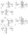
ここで、上記構成よりなる実装装置の動作の一例を図4に従って説明する。
図4の(a)は、第1カメラ20と第2カメラ21のキャリブレーション工程を示す。まず、実装位置に配置されている第1カメラ20と第2カメラ21との間に、吸着ヘッド2の先端部を挿入し、両方のカメラ20,21で吸着ヘッド2に設けられたキャリブレーションマーク6を撮像し、両方のカメラ20,21の光軸ずれ量を求める。光軸のずれ量は、後述する電子部品Pと吸着ヘッド2との相対位置の算出、基板Bとステージ11との相対位置の算出、吸着ヘッド2とステージ11との位置補正などに利用される。
図4の(b)は吸着ヘッド2に吸着されている電子部品Pをカメラ20,21の間、すなわち実装位置に挿入した状態を示す。
図4の(c)は吸着ヘッド2を実装高さまで下降させた状態を示し、この位置で第1カメラ20でヘッド基準マーク5を認識し、第2カメラ21で電子部品P(アライメントマークP1)を認識する。そして、第1カメラ20と第2カメラ21からの画像情報を用いて、電子部品Pの位置(姿勢)と、電子部品Pと吸着ヘッド2との相対位置(姿勢)とを算出し、記憶する。
図4の(d)は吸着ヘッド2を退避させた状態を示す。
図4の(e)はステージ11を実装位置、つまりステージ11上の基板Bを第1カメラ20で認識でき、ステージ11の背後の基準マーク14を第2カメラ21で認識できる位置へ挿入した状態を示す。この位置で第1カメラ20で基板B(アライメントマークB1)を認識し、第2カメラ21でステージ基準マーク14を認識する。そして、第1カメラ20と第2カメラ21からの画像情報を用いて、基板Bの位置(姿勢)と、基板Bとステージ11との相対位置(姿勢)とを算出し、記憶する。この時、図4の(c)で求めた電子部品Pの位置に合うように、基板Bの位置を補正する。
なお、図4の(e)における第1カメラ20、第2カメラ21の焦点距離が、キャリブレーションマーク6を認識した時(図4の(a))の焦点距離と異なるので、アライメントマークB1およびステージ基準マーク14を明確に認識できるように、オートフォーカス機能を用いるのがよい。
図4の(f)は実装工程であり、ステージ11を図4の(e)の位置に保持したまま、吸着ヘッド2を図4の(c)と同じ位置へ移動させ、電子部品Pを基板Bに実装する。図4の(c)で位置認識した後、図4の(d)で退避させ、さらに図4の(f)で実装位置へ戻した時、駆動機構7,8,9の精度によっては電子部品Pが図4の(c)の位置に再現性よく戻れるとは限らない。また、第2カメラ21の視界はステージ11によって遮られているので、電子部品Pを第2カメラ21で直接認識できない。そこで、実装工程では、第1カメラ20でヘッド基準マーク5を認識し、図4の(c)で算出した相対位置データから、電子部品Pの位置が図4の(c)における電子部品Pの位置に合うように吸着ヘッド2をXY方向に移動させる。ステージ11は図4の(e)の位置に保持したままであるから、図4の(e)で認識した位置とずれがなく、電子部品Pの位置補正だけを行なえばよい。なお、θ軸方向のずれがある場合には、ステージ11をθ方向に移動させればよい。
以上のようにして、電子部品Pと基板Bとを正確に位置合わせすることができ、この状態で実装することで高精度な製品を得ることができる。
【0024】
図5は上記実装装置の動作の他の例を示す。
図5の(a)は、第1カメラ20と第2カメラ21のキャリブレーション工程であるが、ここではキャリブレーションマーク19をステージ11に設けてある。そのため、まず第1カメラ20と第2カメラ21とを実装位置へ移動させ、ステージ11の先端部をカメラ20,21の間に挿入し、両方のカメラ20,21でステージ11に設けられたキャリブレーションマーク19を撮像し、両方のカメラ20,21の光軸ずれ量を認識する。
図5の(b)はステージ11を実装位置へ移動させた状態を示す。ここで、ステージ11上に保持された基板B(アライメントマークB1)が第1カメラ20で撮像され、ステージ11の下面に設けられた基準マーク14が第2カメラ21で撮像される。第1カメラ20と第2カメラ21からの画像情報を用いて、基板Bの位置と、基板Bとステージ11との相対位置とが算出され、記憶される。
図5の(c)はステージ11を退避させると同時に、吸着ヘッド2を実装位置へ移動させた状態を示す。
図5の(d)は、吸着ヘッド2を実装高さまで下降させた状態を示し、この位置で第1カメラ20でヘッド基準マーク5を認識し、第2カメラ21で電子部品P(アライメントマークP1)を認識する。つまり、第1カメラ20と第2カメラ21からの画像情報を用いて、電子部品Pの位置と、電子部品Pと吸着ヘッド2との相対位置とを算出し、記憶する。なお、この時、第1カメラ20と第2カメラ21との焦点距離が、キャリブレーションマーク19を認識した時の焦点距離と異なるので、オートフォーカス機能によりヘッド基準マーク5およびアライメントマークP1を明確に認識できるようにするのがよい。
図5の(e)は、吸着ヘッド2を実装高さより上昇させて退避させておき、ステージ11を実装位置へ移動させた状態を示す。ここで、図5の(b)で記憶された位置情報から、図5の(d)の電子部品Pの位置に基板Bが合致するように、ステージ11がX,Y,θ方向に移動される。
図5の(f)は実装工程であり、ステージ11を図5の(e)の位置に保持したまま、吸着ヘッド2を下降させて電子部品Pを基板Bに実装する。このとき、吸着ヘッド2のZ軸駆動機構7が十分な再現性を持たない場合でも、図5の(d)における基準マーク5の位置と(f)の基準マーク5の位置との誤差を認識し、さらにXY方向の補正を加えることで、誤差を解消できる。
以上のようにして、電子部品Pと基板Bとを正確に位置合わせし、実装することができる。
【0025】
図4および図5で示した位置決め工程において、加熱しながら実装を行う場合には、実装途中で吸着ヘッド2またはステージ11が熱変形を起こすことがある。そのため、実装直前には正確に位置合わせされていても、実装が終了した時点で電子部品Pと基板Bとが正確に合致しない場合が生じる。
そのような場合の対策として、実装工程(図4の(f)または図5の(f)参照)において、次のような方法を用いることができる。
まず、ヘッド基準マーク5とステージ基準マーク14とを第1,第2カメラ20,21で認識し、上述の相対位置情報を用いて電子部品Pと基板Bの位置が一致する位置に吸着ヘッド2とステージ11とを仮止めする。この時点では、電子部品Pと基板Bとは軽く接触しているに過ぎない。
次に、吸着ヘッド2およびステージ11の一方もしくは双方を接合のために加熱(例えば350℃/5sec以上)しつつ加圧し、その間、ヘッド基準マーク5とステージ基準マーク14を第1,第2カメラ20,21で連続的に撮像する。そして、上記仮止め工程の相対位置関係を維持するよう、吸着ヘッド2とステージ11とを相対位置補正する。
上記のような方法を用いれば、実装途中にずれが発生しても、そのずれをカメラ20,21によりリアルタイムで検出して補正するので、正確な接合が可能となる。
なお、上記の場合には電子部品Pと基板Bとを軽く接触させて仮止めしたが、電子部品Pと基板Bとを接触させずに直前で仮止めを行ってもよい。
【0026】
−第2実施例−
図6〜図9は本発明にかかる実装装置の第2実施例を示す。
この実施例の実装装置も、ヘッド部30およびステージ部40と、第1,第2の光学系60,61と、制御装置(図示せず)とで構成されている。
ヘッド部30は、電子部品Pを吸着する吸着ヘッド31と、例えばX,Y,Z軸方向に駆動する駆動機構32と、吸着ヘッド31を駆動機構32に連結するブラケット33とで構成されている。ブラケット33は対向する一対の支持壁33aを備えており、その間にX軸方向に貫通した空洞部33bが設けられている。この空洞部33bには、第1光学系60のミラー部60cがX軸方向より出入り自在に挿入される。
【0027】
吸着ヘッド31は、図8に示すようにベース部材34と、ベース部材34の上面に固定された透明ガラスなどからなる透明板35と、ベース部材34の下面に固定された断熱材よりなる筒状部材36と、筒状部材36の下端部に固定されたアタッチメント部材37と、アタッチメント部材37と筒状部材36との間に挟着されたヒータ38とで構成されている。上記ベース部材34は支持壁33aの下端部にネジ等によって固定されている。アタッチメント部材37はできるだけ熱伝導性の良好な材料で形成するのがよい。
【0028】
ベース部材34の中央部には、上下に貫通する穴34aが設けられ、この貫通穴34aは筒状部材36の内部穴36aと連通しており、これら穴34a,36aによって中空部39が形成されている。中空部39の上面が透明板35で閉鎖されている。ベース部材34には、中空部39に連通するエアー配管34bが接続されており、このエアー配管34bは図示しない真空吸引装置と接続され、エアー吸引通路を構成している。
【0029】
ヒータ38の中心部には貫通穴38aが設けられ、この貫通穴38aはアタッチメント部材37の中心部に突設されたボス部37aに嵌合され、ヒータ38はアタッチメント部材37に対して同心状に位置決めされている。アタッチメント部材37のボス部37aの中心には、部品吸着穴37bが貫通形成されている。部品吸着穴37bの下側開口部に電子部品Pが吸着される。
【0030】
上記のように、吸着ヘッド31の部品吸着穴37bの背後に部品吸着穴37bと連通する中空部39が形成され、中空部39の部品吸着穴37bと対向する面が透明板35で閉鎖されている。ヘッド31を駆動機構32に連結するためのブラケット33には空洞部33bが設けられ、この空洞部33bに挿入された第1光学系60で透明板35を介して部品吸着穴37bを容易に認識することができる。つまり、部品吸着穴37bをヘッド基準マークとして用いることができる。なお、回転方向の角度ずれを検出するため、部品吸着穴37bの上側開口部37b1を図9に示すように長方形などの方向性を持つ異形形状とするのがよい。
【0031】
ステージ部40は、基板Pを吸着保持するステージ41と、例えばX,Y,θ軸方向に駆動する駆動機構42と、ステージ41を駆動機構42に連結するブラケット43とで構成されている。ステージ41は吸着ヘッド31と、ブラケット43はブラケット33と上下対称構造であるから、以下に主要部の部品符号を列記して重複説明を省略する。すなわち、43bは空洞部、44はベース部材、44bはエアー配管、45は透明板、46は筒状部材、47はアタッチメント部材、47bは部品吸着穴、48はヒータ、49は中空部である。
この場合も、空洞部43bにX軸方向より挿入された第2光学系61で透明板45を介して部品吸着穴47bを撮像することができ、部品吸着穴47bをヘッド基準マークとして用いることができる。
【0032】
第1光学系60は、XY軸駆動機構62上に設けられた支柱部63にZ1軸駆動機構64を介して取り付けられており、第2光学系61は、上記支柱部63にZ2軸駆動機構65を介して取り付けられている。
第1光学系60は、カメラ60aと、X軸方向に延びる筒形のレンズ60bと、レンズ60bの先端に取り付けられたプリズムまたはミラー60cとを備えており、このミラー60cがブラケット33の空洞部33bに挿入される。そして、部品吸着穴37bの光をミラー60cで反射させ、レンズ60bを介してカメラ60aで撮像できるようになっている。第2光学系61も同様に、カメラ61aと、X軸方向に延びる筒形のレンズ61と、プリズムまたはミラー61cとを備えており、このミラー61cがブラケット43の空洞部43bに挿入される。空洞部33b,43bに比べてミラー60c,61cは小断面であるため、XYZ方向にスペース上の余裕が存在する。そのため、位置認識、実装、位置補正時に吸着ヘッド31およびステージ41を動作させた場合でも、ブラケット33,43とミラー60c,61cとの干渉を防止できる。
【0033】
第1光学系60と第2光学系61は、互いの光軸が同軸で対向し、かつカメラ同士がXY方向に相対移動しないように支柱部63によって支持されている。また、第1光学系60と第2光学系61との光軸ずれ量を認識するため、吸着ヘッド31またはステージ41に設けられた一方の部品吸着穴37b,47bをキャリブレーションマークとして用いることができる。但し、この場合には部品Pまたは基板Bを吸着していない状態でキャリブレーションを行なう必要がある。
大型の基板Bに複数の部品Pを実装する場合に対応するため、両光学系20,21はXY軸駆動機構62によりXY方向に一体に移動可能となっている。
また、第1光学系60をZ1軸駆動機構64によって上下方向に調整し、第2光学系61をZ2軸駆動機構65によって上下方向に調整することで、各光学系60,61のフォーカス調整を独自に行なうことができる。
【0034】
上記実施例の実装装置の動作は、図4または図5に示された動作とほぼ同様である。特に、キャリブレーションとして吸着ヘッド31の部品吸着穴37bまたはステージ41の部品吸着穴47bを使用した場合には、電子部品Pまたは基板Bを吸着する前に吸着ヘッド31またはステージ41を上下の光学系60,61の間に挿入し、光軸ずれ量を測定すればよい。
【0035】
上記実施例では、部品吸着穴37b,47bをヘッド基準マークおよびステージ基準マークとして用いている。部品吸着穴37b,47bは部品Pおよび基板Bと最も近い位置にあるので、吸着ヘッド31やステージ41に多少の変形があっても、部品Pと吸着ヘッド31との相対位置ずれ量、基板Bとステージ41との相対位置ずれ量が最も小さくなる。
また、ヘッド(またはステージ)の背後から透明板を介して基準マークである部品吸着穴を透視可能であるから、実装途中でもヘッド(またはステージ)の位置を正確に認識することができ、精度の高い位置決めが可能となる。
【0036】
また、吸着ヘッド31およびステージ41の双方がヒータ38,48を備えているので、熱と圧力とをかけて電子部品Pを基板Bに実装することができる。この場合、ヒータ38,48が部品吸着穴37b,47bに非常に近い位置に設けられているので、部品Pおよび基板Bに対して熱を最も効率良く伝えることができ、接合性能の向上を図ることができる。また、ヘッド(またはステージ)を加熱すると、周囲の空気の揺らぎによって光学系による撮像画像に歪みが発生し、誤差の原因になるが、中空部39はエアー吸引通路34bからのエアー吸引によって減圧状態にあるので、空気の密度が低く、揺らぎが少ない。そのため、透明板35および中空部39を介して部品吸着穴37bを撮像したとき、揺らぎによる誤差が少なく、精度のよい撮像データを得ることができる。
【0037】
なお、上記実施例では、第1光学系60および第2光学系61に設けられたミラー部60c,61cを空洞部33b,43bに挿入するようにしたが、カメラを小型に構成できる場合には、レンズ部60b,61bやミラー部60c,61cを省略し、直接カメラ60a,61aを空洞部33b,43bに挿入してもよい。
また、吸着ヘッド31とステージ41とを上下対称構造とし、ブラケット33およびブラケット43も上下対称構造としたが、取り扱う第1部品(電子部品)Pおよび第2部品(基板)Bの形状や大きさに応じて任意の構造を採ることができる。
ブラケット33,43として、実施例のような一対の支持壁33aで支持する構造部材を使用したので、吸着ヘッド31およびステージ41を駆動機構32,42に対して両端支持構造で支持することができ、実装時の加圧力による吸着ヘッド31およびステージ41の撓みを防止できる。しかも、ブラケット33,43は光学系60,61のミラー部60c,61cを挿入自在な空洞部33b,43bを有するので、実装途中におけるヘッド基準マーク37b,47bを容易に認識することができる。
【0038】
−第3実施例−
図10,図11は本発明にかかる実装装置の第3実施例であり、1台のカメラで2つの光学系を構成した例である。図6〜図9に示す第2実施例と同一部分には同一符号を付して重複説明を省略する。
この実施例では、支柱部63にZ軸方向に移動可能に設けられたテーブル70上に、カメラ71とレンズ72とカメラ71の視野を上下半分ずつに分割するミラー(またはプリズム)73,74とが設置されている。カメラ71の光軸は、ミラー73によって上向きに曲げられ、Z軸方向に移動不能なレンズ75に設けられた2つのミラー(またはプリズム)76,77によって下向きに曲げられ、ヘッド基準マーク37bを撮像することができる。一方、ミラー74によって下方に向かって曲げられた光軸は、Z軸方向に移動不能なレンズ78に設けられた2つのミラー(またはプリズム)79,80によって上向きに曲げられ、ステージ基準マーク47bを撮像することができる。このように、1台のカメラ71で2つの光学系を構成することができる。
【0039】
図11はカメラ71による視野画像を示す。上半分に写った画像がヘッド基準マーク37bであり、下半分に写った画像がステージ基準マーク47bである。テーブル70をZ軸方向に移動させて、上下の光学系の光路の長さを等しくし、フォーカスをY軸で合わせることで、上下の光学系の画像の焦点を同時に合わせることができる。
【0040】
−第4実施例−
図12,図13は本発明にかかる実装装置の第4実施例である。この実施例は、4台のカメラを用いることで、高速に位置合わせを行う方式である。図12は図1と、図13は図4と対比して説明する。なお、同一部分には同一符号を付して重複説明を省略する。
図12において、第1カメラ81と第2カメラ82とが位置決め手段83によって光軸が対向するように保持され、第3カメラ84と第4カメラ85とが光軸が対向するように位置決め手段86によって保持されている。第1カメラ81と第2カメラ82、第3カメラ84と第4カメラ85は、それぞれXY方向には相対位置が固定され、フォーカス方向には移動自在である。
例えば、第1カメラ81はヘッド基準マーク5を認識するために用いられ、第2カメラ82は吸着ヘッド2に吸着された部品Pを認識するために用いられる。また、第3カメラ84は例えばステージ11に保持された基板Bとヘッド基準マーク5とを認識するために用いられ、第4カメラ85はステージ基準マーク14を認識するために用いられる。
【0041】
上記構成の実装装置の動作を図13にしたがって説明する。
図13の(a)はキャリブレーション工程であり、第1カメラ81と第2カメラ82との間に吸着ヘッド2の先端部を挿入し、両方のカメラ81,82で吸着ヘッド2に設けられたキャリブレーションマーク6を撮像し、両方のカメラ81,82の光軸ずれ量を求める。同様に、第3カメラ84と第4カメラ85との間にステージ11を挿入し、両方のカメラ84,85でステージ11に設けられたキャリブレーションマーク19を撮像し、両方のカメラ84,85の光軸ずれ量を求める。
図13の(b)は吸着ヘッド2に吸着されている電子部品Pをカメラ81,82の間に挿入し、ステージ11に保持されている基板Bをカメラ84,85の間に挿入した状態を示す。この状態で、カメラ81,82によってヘッド基準マーク5と部品Pとの相対位置を認識し、カメラ84,85によって基板Bとステージ基準マーク14との相対位置を認識する。
図13の(c)は吸着ヘッド2とステージ11とを、部品Pと基板Bとが位置合わせされるように移動させた状態を示す。ここでは、第3,第4カメラ84,85の間に吸着ヘッド2を移動させ、第3カメラ84でヘッド基準マーク5を認識し、第4カメラ85でステージ基準マーク14を認識したが、第1,第2カメラ81,82の間にステージ11を移動させ、第1カメラ81でヘッド基準マーク5を認識し、第2カメラ82でステージ基準マーク14を認識してもよい。
図13の(d)は接合工程であり、部品Pと基板Bとを加熱しながら接合を行う。加熱によって部品Pと基板Bの相対位置がずれないように、第3,第4カメラ84,85で連続的にマーク5,14を撮像し、リアルタイムで吸着ヘッド2またはステージ11を位置補正するのがよい。
上記のように、4台のカメラ81,82,84,85を使用すれば、一方のカメラ対で吸着ヘッド2側を撮像している間に、他方のカメラ対でステージ11側を撮像できるので、位置合わせおよび実装を高速で行うことができる。
【0042】
図14,図15は本発明にかかる部品装着方法で用いられる光部品の例を示す。この実施例は、第1部品として面発光型レーザダイオード(以下、LDと呼ぶ)90を用い、第2部品として光導波路基板100を用いたものである。
LD90は、図11に示すように1つの主面の中央部に発光部91を有し、この発光部91から略円錐形の射出光が射出される。光導波路基板100の上面には光導入孔101が所定間隔で垂直方向に形成され、基板100の内部には光導入孔101と直交する導波路102が水平方向に形成されている。LD90は、光導波路基板100の上面に、光導入孔101に対して発光部91を位置合わせして下向きに導電性接合材(金属接合材)103で接合されている。LD90の光は、光導入孔101から導波路102を通って図示しない光通信回線へ送られる。
【0043】
上記のようなLD90と光導波路基板100とを正確に位置合わせして接合する場合に、本発明方法を使用することができる。
第1,第2実施例では、第1部品P,第2部品BにそれぞれアライメントマークP1,B1を設けたが、第3実施例ではLD90の発光部91をアライメントマークとして利用し、光導波路基板100の光導入孔101をアライメントマークとして利用することができる。
そのため、LD90および光導波路基板100に格別なアライメントマークを設ける必要がない。特に、LD90の場合、発光部91の位置が重要であり、発光部以外の位置にアライメントマークを設けても、そのアライメントマークと発光部との間にバラツキがあると、LD90を光導波路基板100に正確に実装できない。上記のように発光部91および光導入孔101をアライメントマークとして利用することで、作業工数の削減だけでなく、精度も向上する。
【0044】
上記実施例では、1枚の基板Bに対して1個の電子部品Pを装着する例について説明したが、1枚の基板Bに対して複数個の電子部品Pを装着する場合でも同様である。ただし、その場合には、基板Bの複数の装着位置にそれぞれアライメントマークB1を設けるとともに、これに対応するステージ11にも複数のステージ基準マーク14を設ける必要がある。
【0045】
本発明は、半導体チップなどの電子部品を基板に搭載するチップマウンタや、TABボンダ、フリップチップボンダなど、広い用途に用いることができる。
本発明の部品装着装置は、図1または図6に示された構造に限るものではなく、本発明の各工程を実施できる構造であればよい。
本発明において、第1カメラを吸着ヘッドより上方に配置し、第2カメラをステージより下方に配置したが、少なくともヘッド基準マークおよびステージ基準マークからの光を受ける部分(例えばレンズやミラーなど)が吸着ヘッドより上方およびステージより下方に位置すればよく、カメラ本体がそれぞれ吸着ヘッドより上方、ステージより下方に配置されている必要はない。したがって、複数のミラーやプリズムを用いて吸着ヘッドの側方や下方、あるいはステージの側方や下方に配置されたカメラ本体に光を反射するようにしてもよい。
【0046】
【発明の効果】
以上の説明で明らかなように、請求項1に記載の発明によれば、装着作業中の位置保証を、ヘッドとステージの双方に設けた基準マークを撮像しながら行なうため、ヘッドとステージとを駆動する軸機構として必要な精度を位置分解能だけとすることができ、高精度な再現性を必要としない。そのため、安価な軸機構を採用しながら、極めて高精度な装着を行なうことができる。
また、装着作業を2つの光学系で上下から撮像しながら実施できるので、熱変形やロストモーションなどの再現性誤差は、装着作業中に補正が可能である。そのため、加熱条件下でも精度のよい位置決めが可能である。
【0047】
また、請求項6に記載の発明によれば、請求項1に係る部品装着方法を簡単な装置で実現できる。
【図面の簡単な説明】
【図1】本発明にかかる部品装着方法を用いた実装装置の第1実施例の斜視図である。
【図2】図1に示す実装装置の吸着ヘッドおよびステージの拡大図である。
【図3】図1に示す実装装置の吸着ヘッドおよびステージの斜視図である。
【図4】図1に示す実装装置の位置合わせ動作を示す動作説明図である。
【図5】図1に示す実装装置の位置合わせ動作の他の例の動作説明図である。
【図6】本発明にかかる部品装着方法を用いた実装装置の第2実施例の正面図である。
【図7】図6のVII−VII 線断面図である。
【図8】図6に示す実装装置の吸着ヘッドの拡大図であり、(a)は正面図、(b)はVIII−VIII 線断面図である。
【図9】吸着ヘッドに設けられた部品吸着穴の背後から見た拡大図であり、(a)は正面図、(b)はIX−IX 線断面図である。
【図10】本発明にかかる実装装置の第3実施例の側面図である。
【図11】図10に示すカメラで撮像した視野画像図である。
【図12】本発明にかかる実装装置の第4実施例の斜視図である。
【図13】図12に示す実装装置の動作説明図である。
【図14】本発明にかかる部品装着方法を用いて実装した光部品の断面図である。
【図15】図14の光部品に用いられるレーザダイオードの斜視図である。
【符号の説明】
P 電子部品(第1部品)
B 基板(第2部品)
1a ヘッド部
1b ステージ部
2 吸着ヘッド
4 部品吸着穴
5 ヘッド基準マーク
6 キャリブレーションマーク
7,8,9 ヘッド用駆動機構
11 ステージ
13 部品吸着穴
14 ステージ基準マーク
15,16,17 ステージ用駆動機構
20 第1光学系
21 第2光学系
25 制御装置[0001]
TECHNICAL FIELD OF THE INVENTION
The present invention relates to a component mounting method and a component mounting apparatus used when mounting an electronic component on a substrate or the like.
[0002]
[Prior art]
[Patent Document 1] Japanese Patent No. 2780000
[Patent Document 2] Japanese Patent No. 2811856
2. Description of the Related Art Conventionally, when an electronic component such as a semiconductor chip or a piezoelectric component is mounted on a substrate such as a printed circuit board, a high-precision positioning mechanism is required to accurately mount the electronic component at a predetermined position on the substrate.
[0003]
Examples of such a positioning mechanism include those described in
[0004]
[Problems to be solved by the invention]
However, in the case of
[0005]
On the other hand, in the case of
[0006]
Therefore, an object of the present invention is to enable high-precision positioning while using an inexpensive shaft mechanism for moving components, and to recognize the position of the head or stage during mounting, and An object of the present invention is to provide a component mounting method and a component mounting device that can correct an error due to deformation or the like.
[0007]
[Means for Solving the Problems]
In order to achieve the above object, an invention according to
[0008]
According to a sixth aspect of the present invention, there is provided a component mounting apparatus for positioning and mounting a first component and a second component, the suction head having a head reference mark which sucks the first component at a lower end and can be recognized from above. A stage holding a second component at an upper end thereof and having a stage reference mark recognizable from below, a driving mechanism for relatively moving the suction head and the stage in X, Y, Z and θ directions; A first optical system for imaging the second component and the head reference mark held on the stage from above, and disposed so as to be substantially opposed to the optical axis of the first optical system, and sucked by the suction head from below the stage; A second optical system for imaging the first component and the stage reference mark, and the relative position between the first component and the suction head, the second component and the stay using the image information from the first and second optical systems. An arithmetic unit for calculating the relative position of the head, the head reference mark and the stage reference mark are recognized by the first and second optical systems in a state where the suction head and the stage are moved to the mounting position. And a controller that corrects the position of the suction head and the stage so that the positions of the first component and the second component have a predetermined relationship using the positional information and the relative position information described above. Component mounting apparatus.
[0009]
An example of the component mounting method according to
First, a first optical system and a second optical system are prepared. Here, the optical system includes not only a single camera but also a mirror, a lens, and the like. One optical system is not limited to one having one camera, and two optical systems are configured by one camera. It is also possible that one optical system is constituted by a plurality of cameras.
The first optical system is arranged with the optical axis directed downward from above the suction head, and the second optical system is arranged with the optical axis directed upward from below the stage. The optical axes of the first optical system and the second optical system are substantially opposed, and have a known positional relationship with each other. The range in which the optical axes are substantially opposed to each other includes a shift that allows the optical axes of the optical systems opposed to each other to enter. When the size of the target first component and second component is larger than the expected visual field, it is preferable that the first optical system and the second optical system can be moved in the horizontal direction while being integrated.
Next, the suction head is inserted between the first optical system and the second optical system, and a head reference mark provided to the suction head and recognized from above by the first optical system is imaged. An image of the sucked first component is taken. Since the optical axes of the first optical system and the second optical system are substantially opposed to each other, the relative position between the suction head and the first component can be obtained from the image data of the two optical systems. The insertion of the suction head between the first optical system and the second optical system is not limited to the case where the first and second optical systems are fixed and the suction head is moved. 1 and the case where the second optical system is moved is also included.
Next, the stage is inserted between the first optical system and the second optical system, the first optical system captures an image of the second component held on the stage, and the second optical system applies the stage to the stage and applies the image to the stage from below. An image of a recognizable stage reference mark is taken. Also in this case, the relative position between the stage and the second component can be obtained from the imaging data of the two optical systems, as described above. Note that inserting the stage between the first optical system and the second optical system is not limited to the case where the first and second optical systems are fixed and the stage is moved, but the case where the stage is fixed and the first and second optical systems are fixed. The case where the second optical system is moved is also included.
It should be noted that the step of determining the relative position between the suction head and the first component and the step of determining the relative position between the stage and the second component may be performed first. The head reference mark is preferably provided at a position as close as possible to the first component sucked by the suction head, and the stage reference mark is preferably provided at a position as close as possible to the second component. When photographing the first part and the second part, an alignment mark may be added to these parts in advance, or a feature point (for example, an edge) of the part is imaged to recognize the position of the part. Is also good.
Next, the relative position between the first component and the suction head and the relative position between the second component and the stage are calculated using the image information from the first optical system and the second optical system. In other words, the position of the suction head (head reference mark) is recognized from the image information of the first optical system, and the position of the first component is recognized from the image information of the second optical system. The position can be calculated. The relative position between the second component and the stage can be determined by recognizing the position of the second component from the image information of the first optical system and recognizing the position of the stage (stage reference mark) from the image information of the second optical system. Can be calculated.
Next, with the suction head and the stage moved to the mounting position, the head reference mark and the stage reference mark are recognized by the first and second optical systems. The position of the suction head and the stage is corrected so that the positions of the first component and the second component have a predetermined relationship. If the first component and the second component are mounted in this state, they can be mounted in a state where they are aligned with high accuracy without mutual displacement.
[0010]
In the method of the present invention, since the position is assured during the mounting operation while imaging the reference marks provided on both the head and the stage, the accuracy required for the shaft mechanism can be limited to only the position resolution, and high-precision reproduction is possible. Does not require sex. Therefore, an inexpensive shaft mechanism can be adopted. In addition, reproducibility errors such as thermal deformation and lost motion can be corrected during mounting work. As a result, the present invention is applicable to the mounting of electronic components requiring positional accuracy on the order of submicrons.
The first and second optical systems do not need to be kept in a fixed positional relationship at all times, and may be in a known positional relationship at least at the time of imaging. For example, one of the optical systems may be temporarily retracted when the head or the stage is inserted, and then returned to the original position. In this case, it is necessary to use a reproducible mechanism for moving the optical system.
Further, since the positioning operation can be performed while capturing images with the first and second optical systems, it is possible to detect a shift between the first and second components during the mounting operation. Therefore, for example, in the bump bonding method, even if the head or the stage is thermally deformed by the heat of the heater, the position of the first and second components can be corrected by recognizing the thermal deformation as needed, so that the accuracy can be improved even under the heating condition. Good positioning is possible.
The head reference mark in the present invention is not limited to a mark such as a colored mark or an uneven portion specially given to the suction head, but may be a part such as an edge portion of the head. Similarly, the stage reference mark is not limited to a mark specially given to the stage, but may be a part such as an edge portion of the stage.
In the present invention, the term “position” generically represents the position in the X, Y, and Z directions and the direction in the θ direction. Therefore, the position also includes the concept of posture.
[0011]
In the step of preparing the first optical system and the second optical system, a single calibration mark that can be recognized from above and below is inserted between the first optical system and the second optical system. Alternatively, the method may include a step of measuring the optical axis shift amount between the first optical system and the second optical system by imaging the calibration mark with the first optical system and the second optical system.
Even if the optical axis of the first optical system and the optical axis of the second optical system are adjusted in advance so that they are coaxial and accurately oppose to each other, it is inevitable that the optical axis will shift due to the passage of time, temperature change, etc. It is difficult to maintain high-precision position accuracy such as on the order of microns. Therefore, the first optical system and the second optical system recognize the same mark from both the upper and lower sides to determine the amount of deviation of the optical axes of both optical systems, and use this amount of optical axis deviation to determine the first component and the first component. If the calculation of the relative position of the suction head, the calculation of the relative position of the second component and the stage, and the correction of the position of the suction head and the stage are performed, no error is added and accurate positioning can be performed.
The highest accuracy can be maintained by performing the calibration every time the component is mounted. However, the calibration may be performed every set number of times or every set time.
[0012]
The calibration mark may be a mark provided on the suction head or the stage.
Although it is possible to provide the calibration mark on a member different from the suction head and the stage, this requires a moving mechanism for moving the separate member in and out between the first optical system and the second optical system. The device becomes complicated. Therefore, if the calibration mark is provided on the suction head or the stage, there is an advantage that a separate member for calibration is not required and the structure is simplified.
Note that the calibration mark needs to be simultaneously recognizable from the upper and lower optical systems. Therefore, the upper and lower through holes provided on the suction head or the stage, the marks provided on the transparent body (glass plate), and the like can be used as the calibration marks.
[0013]
The step of imaging the first optical system and the second optical system with the head reference mark and the first component, the image of the second component and the stage reference mark with the suction head, During the step of correcting the position of at least one of the stages and the step of mounting the first component and the second component, it is preferable to maintain a fixed positional relationship. In other words, it is preferable that the optical systems be kept at all times during the alignment process so that the optical axes of the optical systems do not shift.
If the position is recognized using the first and second optical systems whose relative positions are fixed so as to always face each other, the influence of the error caused by the moving mechanism is reduced as compared with the case where the optical systems are moved mutually. Since it can be reduced, the positioning accuracy can be increased, and an advanced moving mechanism is not required.
[0014]
According to a fifth aspect of the present invention, in the step of correcting the position of the suction head and the stage at the mounting position, the head reference mark and the stage reference mark are moved while heating one or both of the suction head and the stage for bonding. The method may include a step of continuously imaging with two optical systems and correcting the relative positions of the suction head and the stage so that the positions of the first component and the second component have a predetermined relationship using the relative position information. .
In this case, since the displacement of the mark is continuously imaged with respect to the thermal deformation during the mounting work, the position can be corrected in real time even if the thermal deformation occurs, and the first component and the second component are always accurately corrected. Parts can be mounted.
[0015]
As in claim 8, at least one of the suction head and the stage is provided behind the component suction hole, a hollow portion communicating with the component suction hole, and a surface facing the component suction hole of the hollow portion. And a transparent body through which the component suction hole can be seen from behind, and an air suction passage connected to the hollow portion, and at least one of the first optical system and the second optical system is provided through the transparent body. The component suction hole may be configured to be recognized as a head reference mark or a stage reference mark.
That is, the component suction hole is a hole for sucking the first component or the second component, and is located closest to the component. Therefore, even if the suction head or the stage is thermally deformed, the amount of relative positional deviation from the component can be minimized.
Also, since the component suction hole serving as the reference mark can be seen through the transparent body from behind the head (or stage), it is possible to easily capture an image from behind the head (or stage) by an optical system even during mounting. . That is, since the position of the head (or stage) during mounting can be accurately recognized, highly accurate positioning is possible.
[0016]
As described in claim 9, a heater for heating may be fixed near the component suction hole.
When mounting the first component and the second component, they may be joined by applying heat and pressure. In this case, if the heater is provided at a position closest to the component, that is, in the vicinity of the component suction hole, heat can be transmitted to the component most efficiently, so that the bonding performance can be improved.
When the head (or the stage) is heated, the image picked up by the optical system is distorted due to the fluctuation of the surrounding air, which causes an error. However, when the suction head or the stage having the structure of claim 8 is used, the hollow portion is also heated by the heat of the heater, but the hollow portion is in a state where the pressure is reduced by the air suction from the air suction passage. Low density and little fluctuation. Therefore, when an image of the component suction hole is taken through the transparent body and the hollow portion, an error due to fluctuation is small, and highly accurate image data can be obtained.
[0017]
According to the tenth aspect, the back surface of the suction head or the stage is attached to the drive mechanism via a bracket, and the first or second optical system for imaging the component suction hole is inserted into the bracket via the transparent body. It is preferable to form a free cavity.
The head (or stage) is driven in the X-, Y-, Z-, or θ-axis directions by a driving mechanism. However, when this head is supported by the driving mechanism in a cantilever structure, the back of the transparent body is open. It is easy to arrange a camera or a mirror behind the transparent body. However, since the head having the cantilever support structure may be bent by the pressing force when the first component and the second component are joined, it is difficult to perform high-precision joining. On the other hand, when the back of the head is supported by a drive mechanism or the like via the bracket, it is difficult to bend even when a pressing force is applied, and high-precision bonding can be performed. However, it is difficult to arrange a camera or the like behind because the bracket is in the way. Therefore, by supporting with a bracket having a hollow portion behind the head, especially behind the transparent body, the camera does not interfere with the bracket, the component suction hole can be easily imaged, and the head (or stage) is used as a drive mechanism. Can be stably supported.
In the present invention, the optical system includes, in addition to the camera, a part having a function of reflecting an image toward the camera using a mirror, a prism, or the like. Therefore, only imaging optical components such as a mirror, a prism, and a lens other than the camera may be inserted into the cavity.
[0018]
BEST MODE FOR CARRYING OUT THE INVENTION
-1st Example-
1 to 3 show a first embodiment of a mounting apparatus using a component mounting method according to the present invention. Here, the electronic component P was used as the first component, and the substrate B was used as the second component. The mounting apparatus of this embodiment includes a head unit 1a, a
[0019]
The head unit 1a includes a
At the tip of the
The
The
The
[0020]
The
The
The
The
[0021]
A
The
[0022]
The
[0023]
Here, an example of the operation of the mounting apparatus having the above configuration will be described with reference to FIG.
FIG. 4A shows a calibration process of the
FIG. 4B shows a state in which the electronic component P sucked by the
FIG. 4C shows a state in which the
FIG. 4D shows a state in which the
FIG. 4E shows a state in which the
Since the focal lengths of the
FIG. 4F shows a mounting process, in which the
As described above, the electronic component P and the substrate B can be accurately positioned, and a high-precision product can be obtained by mounting in this state.
[0024]
FIG. 5 shows another example of the operation of the mounting apparatus.
FIG. 5A shows a calibration process of the
FIG. 5B shows a state in which the
FIG. 5C shows a state where the
FIG. 5D shows a state in which the
FIG. 5E shows a state in which the
FIG. 5F shows a mounting process in which the electronic component P is mounted on the substrate B by lowering the
As described above, the electronic component P and the board B can be accurately aligned and mounted.
[0025]
In the positioning step shown in FIGS. 4 and 5, when mounting is performed while heating, the
As a countermeasure in such a case, the following method can be used in the mounting process (see FIG. 4F or FIG. 5F).
First, the
Next, one or both of the
If the above method is used, even if a shift occurs during mounting, the shift is detected in real time by the
In the above case, the electronic component P and the substrate B are lightly contacted and temporarily fixed. However, the temporary fixing may be performed immediately before the electronic component P and the substrate B are not contacted.
[0026]
-2nd Example-
6 to 9 show a second embodiment of the mounting apparatus according to the present invention.
The mounting apparatus of this embodiment also includes a
The
[0027]
As shown in FIG. 8, the
[0028]
A
[0029]
A through hole 38a is provided in the center of the
[0030]
As described above, the
[0031]
The
Also in this case, the
[0032]
The first
The first
[0033]
The first
In order to cope with a case where a plurality of components P are mounted on a large-sized board B, both
Further, by adjusting the first
[0034]
The operation of the mounting apparatus of the above embodiment is almost the same as the operation shown in FIG. 4 or FIG. In particular, when the
[0035]
In the above embodiment, the component suction holes 37b and 47b are used as a head reference mark and a stage reference mark. Since the component suction holes 37b and 47b are located closest to the component P and the board B, even if the
In addition, since the component suction hole, which is a reference mark, can be seen through the transparent plate from behind the head (or stage), the position of the head (or stage) can be accurately recognized even during mounting, and accuracy can be improved. High positioning becomes possible.
[0036]
Further, since both the
[0037]
In the above embodiment, the
The
Since the structural members supported by the pair of
[0038]
-Third embodiment-
FIGS. 10 and 11 show a third embodiment of the mounting apparatus according to the present invention, in which one camera constitutes two optical systems. The same parts as those of the second embodiment shown in FIGS. 6 to 9 are denoted by the same reference numerals, and redundant description will be omitted.
In this embodiment, a
[0039]
FIG. 11 shows a visual field image obtained by the
[0040]
-Fourth embodiment-
12 and 13 show a fourth embodiment of the mounting apparatus according to the present invention. In this embodiment, a high-speed alignment is performed by using four cameras. FIG. 12 is described in comparison with FIG. 1 and FIG. 13 is described in comparison with FIG. Note that the same portions are denoted by the same reference numerals, and redundant description will be omitted.
In FIG. 12, a
For example, the
[0041]
The operation of the mounting apparatus having the above configuration will be described with reference to FIG.
FIG. 13A shows a calibration step in which the tip of the
FIG. 13B shows a state in which the electronic component P sucked by the
FIG. 13C shows a state in which the
FIG. 13D shows a joining step in which the component P and the board B are joined while being heated. The third and
As described above, if the four
[0042]
14 and 15 show examples of optical components used in the component mounting method according to the present invention. In this embodiment, a surface emitting laser diode (hereinafter, referred to as LD) 90 is used as a first component, and an
As shown in FIG. 11, the
[0043]
The method of the present invention can be used when the above-described
In the first and second embodiments, the first part P and the second part B are provided with the alignment marks P1 and B1, respectively. However, in the third embodiment, the
Therefore, it is not necessary to provide a special alignment mark on the
[0044]
In the above embodiment, an example in which one electronic component P is mounted on one substrate B has been described. However, the same applies to a case where a plurality of electronic components P are mounted on one substrate B. . In this case, however, it is necessary to provide alignment marks B1 at a plurality of mounting positions of the substrate B, and to provide a plurality of stage reference marks 14 on the
[0045]
INDUSTRIAL APPLICABILITY The present invention can be used for a wide range of applications such as a chip mounter for mounting an electronic component such as a semiconductor chip on a substrate, a TAB bonder, and a flip chip bonder.
The component mounting apparatus of the present invention is not limited to the structure shown in FIG. 1 or FIG. 6, but may be any structure that can perform each step of the present invention.
In the present invention, the first camera is arranged above the suction head, and the second camera is arranged below the stage. At least a portion (for example, a lens or a mirror) that receives light from the head reference mark and the stage reference mark is provided. It is sufficient that the camera body is located above the suction head and below the stage, and the camera body does not need to be arranged above the suction head and below the stage respectively. Therefore, a plurality of mirrors or prisms may be used to reflect light to a camera body arranged on the side or below the suction head or on the side or below the stage.
[0046]
【The invention's effect】
As is apparent from the above description, according to the first aspect of the present invention, position assurance during the mounting operation is performed while imaging the reference marks provided on both the head and the stage. The accuracy required for the driving shaft mechanism can be only the position resolution, and high-precision reproducibility is not required. Therefore, extremely accurate mounting can be performed while employing an inexpensive shaft mechanism.
Further, since the mounting operation can be performed while capturing images from above and below with the two optical systems, reproducibility errors such as thermal deformation and lost motion can be corrected during the mounting operation. Therefore, accurate positioning is possible even under heating conditions.
[0047]
According to the invention described in
[Brief description of the drawings]
FIG. 1 is a perspective view of a first embodiment of a mounting apparatus using a component mounting method according to the present invention.
FIG. 2 is an enlarged view of a suction head and a stage of the mounting apparatus shown in FIG.
FIG. 3 is a perspective view of a suction head and a stage of the mounting apparatus shown in FIG.
FIG. 4 is an operation explanatory diagram showing a positioning operation of the mounting apparatus shown in FIG. 1;
FIG. 5 is an operation explanatory diagram of another example of the positioning operation of the mounting apparatus shown in FIG. 1;
FIG. 6 is a front view of a second embodiment of the mounting apparatus using the component mounting method according to the present invention.
FIG. 7 is a sectional view taken along line VII-VII of FIG. 6;
8 is an enlarged view of the suction head of the mounting apparatus shown in FIG. 6, (a) is a front view, and (b) is a sectional view taken along line VIII-VIII.
FIGS. 9A and 9B are enlarged views of the component suction hole provided in the suction head as viewed from behind, FIG. 9A is a front view, and FIG. 9B is a cross-sectional view taken along line IX-IX.
FIG. 10 is a side view of a third embodiment of the mounting apparatus according to the present invention.
FIG. 11 is a view of a field of view image captured by the camera shown in FIG. 10;
FIG. 12 is a perspective view of a fourth embodiment of the mounting apparatus according to the present invention.
13 is an operation explanatory view of the mounting apparatus shown in FIG.
FIG. 14 is a cross-sectional view of an optical component mounted using the component mounting method according to the present invention.
15 is a perspective view of a laser diode used for the optical component in FIG.
[Explanation of symbols]
P Electronic component (first component)
B board (second component)
1a Head
1b Stage part
2 Suction head
4 Parts suction hole
5 Head reference mark
6 Calibration mark
7,8,9 Head drive mechanism
11 stages
13 Parts suction hole
14 Stage fiducial mark
15,16,17 Stage drive mechanism
20 First optical system
21 Second optical system
25 Control device
Claims (10)
上記吸着ヘッドの上方より光軸を下方に向けた第1光学系と、上記ステージの下方より光軸を第1光学系の光軸と略対向するよう上方に向けた第2光学系とを準備する工程と、
第1光学系と第2光学系との間に吸着ヘッドを挿入し、第1光学系で吸着ヘッドに付与され上方から認識できるヘッド基準マークを撮像するとともに、第2光学系で吸着ヘッドに吸着された第1部品を撮像する工程と、
第1光学系と第2光学系との間にステージを挿入し、第1光学系でステージ上に保持された第2部品を撮像するとともに、第2光学系でステージに付与され下方から認識できるステージ基準マークを撮像する工程と、
上記第1,第2の光学系からの画像情報を用いて第1部品と吸着ヘッドの相対位置、第2部品とステージの相対位置を算出する工程と、
上記吸着ヘッドとステージとを装着位置へ移動させた状態で、上記ヘッド基準マークとステージ基準マークとを上記第1,第2の光学系で認識し、これらの位置情報と上記相対位置情報とを用いて、第1部品と第2部品の位置が所定の関係となるように吸着ヘッドおよびステージの少なくとも一方を位置補正する工程と、上記位置補正後、第1部品と第2部品とを装着する工程と、を備えたことを特徴とする部品装着方法。In a method of sucking a first component with a suction head, aligning the first component with a second component held on a stage, and mounting the first component,
A first optical system whose optical axis is directed downward from above the suction head and a second optical system whose optical axis is directed upward from below the stage so as to substantially oppose the optical axis of the first optical system are prepared. The process of
The suction head is inserted between the first optical system and the second optical system, and the first optical system picks up an image of a head reference mark provided to the suction head and can be recognized from above, and the second optical system suctions the suction head. Imaging the obtained first component;
A stage is inserted between the first optical system and the second optical system, and the first optical system captures an image of the second component held on the stage, and the second optical system applies the stage to the stage and recognizes it from below. Imaging a stage fiducial mark;
Calculating a relative position between the first component and the suction head and a relative position between the second component and the stage using the image information from the first and second optical systems;
With the suction head and the stage moved to the mounting position, the head reference mark and the stage reference mark are recognized by the first and second optical systems, and the position information and the relative position information are determined. A step of correcting the position of at least one of the suction head and the stage so that the positions of the first component and the second component have a predetermined relationship; and mounting the first component and the second component after the position correction. And a step of mounting the component.
第1光学系と第2光学系との間に上下両方から認識できる単一のキャリブレーションマークを挿入し、このキャリブレーションマークを第1光学系と第2光学系とで撮像することで、第1光学系と第2光学系の光軸ずれ量を測定する工程を含むことを特徴とする請求項1に記載の部品装着方法。The step of preparing the first optical system and the second optical system includes:
By inserting a single calibration mark that can be recognized from above and below between the first optical system and the second optical system, and capturing the calibration mark with the first optical system and the second optical system, 2. The component mounting method according to claim 1, further comprising a step of measuring an optical axis shift amount between the first optical system and the second optical system.
下端部に第1部品を吸着し、上方から認識できるヘッド基準マークを有する吸着ヘッドと、
上端部に第2部品を保持し、下方から認識できるステージ基準マークを有するステージと、
上記吸着ヘッドおよびステージをX,Y,Zおよびθ方向に相対移動させる駆動機構と、
上記吸着ヘッドの上方からステージに保持された第2部品とヘッド基準マークとを撮像する第1光学系と、
第1光学系の光軸と略対向するように配置され、上記ステージの下方から吸着ヘッドに吸着された第1部品とステージ基準マークとを撮像する第2光学系と、
上記第1,第2の光学系からの画像情報を用いて、第1部品と吸着ヘッドの相対位置、第2部品とステージの相対位置を算出する演算装置と、
上記吸着ヘッドとステージとを装着位置へ移動させた状態で、上記ヘッド基準マークとステージ基準マークとを上記第1,第2の光学系で認識し、これらの位置情報と上述の相対位置情報とを用いて、第1部品と第2部品の位置が所定の関係となるように吸着ヘッドとステージとを位置補正する制御装置と、を備えたことを特徴とする部品装着装置。In a component mounting apparatus for positioning and mounting a first component and a second component,
A suction head having a head reference mark which sucks the first component at a lower end portion and can be recognized from above;
A stage that holds the second component at the upper end and has a stage reference mark that can be recognized from below;
A drive mechanism for relatively moving the suction head and the stage in the X, Y, Z and θ directions;
A first optical system for imaging the second component and the head reference mark held on the stage from above the suction head;
A second optical system arranged to substantially oppose the optical axis of the first optical system and imaging the first component and the stage reference mark sucked by the suction head from below the stage;
An arithmetic unit that calculates a relative position between the first component and the suction head and a relative position between the second component and the stage using the image information from the first and second optical systems;
With the suction head and the stage moved to the mounting position, the head reference mark and the stage reference mark are recognized by the first and second optical systems, and the position information and the relative position information are recognized. And a control device for correcting the position of the suction head and the stage so that the positions of the first component and the second component have a predetermined relationship.
部品吸着穴と、上記部品吸着穴の背後に設けられ、部品吸着穴と連通する中空部と、上記中空部の部品吸着穴と対向する面を閉鎖し、部品吸着穴を背後から透視可能な透明体と、上記中空部に接続されたエアー吸引通路とを備え、
上記第1光学系および第2の光学系の少なくとも一方は、上記透明体を介して部品吸着穴をヘッド基準マークまたはステージ基準マークとして認識することを特徴とする請求項6または7に記載の部品装着装置。At least one of the suction head and the stage is
A component suction hole, a hollow portion provided behind the component suction hole and communicating with the component suction hole, and a surface facing the component suction hole of the hollow portion is closed, and the component suction hole is transparent from behind. A body, and an air suction passage connected to the hollow portion,
8. The component according to claim 6, wherein at least one of the first optical system and the second optical system recognizes the component suction hole as a head reference mark or a stage reference mark via the transparent body. Mounting device.
上記ブラケットには上記透明体を介して部品吸着穴を撮像するための第1または第2の光学系を挿入自在な空洞部が形成されていることを特徴とする請求項8または9に記載の部品装着装置。The back surface of the suction head or the stage is attached to the drive mechanism via a bracket,
10. The bracket according to claim 8, wherein a cavity is formed in the bracket, through which the first or second optical system for imaging the component suction hole can be inserted through the transparent body. Component mounting device.
Priority Applications (8)
| Application Number | Priority Date | Filing Date | Title |
|---|---|---|---|
| JP2003197179A JP4046030B2 (en) | 2002-08-30 | 2003-07-15 | Component mounting method and component mounting apparatus |
| US10/647,007 US7134188B2 (en) | 2002-08-30 | 2003-08-22 | Parts mounting apparatus |
| CNB031577644A CN1272994C (en) | 2002-08-30 | 2003-08-28 | Element mounting method and its element mounting device |
| EP03255399A EP1395106B1 (en) | 2002-08-30 | 2003-08-29 | Parts mounting method and parts mounting apparatus |
| DE60336698T DE60336698D1 (en) | 2002-08-30 | 2003-08-29 | Method and device for assembling components |
| AT03255399T ATE505941T1 (en) | 2002-08-30 | 2003-08-29 | METHOD AND DEVICE FOR ASSEMBLING COMPONENTS |
| KR1020030060253A KR100540934B1 (en) | 2002-08-30 | 2003-08-29 | Parts mounting method and parts mounting apparatus |
| US11/154,364 US7200926B2 (en) | 2002-08-30 | 2005-06-15 | Parts mounting method |
Applications Claiming Priority (2)
| Application Number | Priority Date | Filing Date | Title |
|---|---|---|---|
| JP2002252396 | 2002-08-30 | ||
| JP2003197179A JP4046030B2 (en) | 2002-08-30 | 2003-07-15 | Component mounting method and component mounting apparatus |
Publications (2)
| Publication Number | Publication Date |
|---|---|
| JP2004146785A true JP2004146785A (en) | 2004-05-20 |
| JP4046030B2 JP4046030B2 (en) | 2008-02-13 |
Family
ID=31497692
Family Applications (1)
| Application Number | Title | Priority Date | Filing Date |
|---|---|---|---|
| JP2003197179A Expired - Fee Related JP4046030B2 (en) | 2002-08-30 | 2003-07-15 | Component mounting method and component mounting apparatus |
Country Status (7)
| Country | Link |
|---|---|
| US (2) | US7134188B2 (en) |
| EP (1) | EP1395106B1 (en) |
| JP (1) | JP4046030B2 (en) |
| KR (1) | KR100540934B1 (en) |
| CN (1) | CN1272994C (en) |
| AT (1) | ATE505941T1 (en) |
| DE (1) | DE60336698D1 (en) |
Cited By (14)
| Publication number | Priority date | Publication date | Assignee | Title |
|---|---|---|---|---|
| WO2008001605A1 (en) * | 2006-06-30 | 2008-01-03 | Nippon Seiki Co., Ltd. | Indicating instrument |
| JP2008140890A (en) * | 2006-11-30 | 2008-06-19 | Fujitsu Ltd | Observation device for assembled status of component and observation method of assembled status of component employing it |
| JP2008149410A (en) * | 2006-12-18 | 2008-07-03 | Ricoh Co Ltd | Method and apparatus for joining components |
| WO2009041003A1 (en) * | 2007-09-28 | 2009-04-02 | Panasonic Corporation | Inspecting device and inspecting method |
| JP2010541293A (en) * | 2007-10-09 | 2010-12-24 | エセック エージー | Method for picking up a semiconductor chip from a wafer table and mounting the removed semiconductor chip on a substrate |
| JP2011029490A (en) * | 2009-07-28 | 2011-02-10 | Shindengen Electric Mfg Co Ltd | Device for mounting component, and method of mounting component |
| JP2011066189A (en) * | 2009-09-17 | 2011-03-31 | Panasonic Corp | Component crimping device |
| JP2012069731A (en) * | 2010-09-24 | 2012-04-05 | Hitachi High-Tech Instruments Co Ltd | Die bonder and manufacturing method of semiconductor |
| JP2016139750A (en) * | 2015-01-29 | 2016-08-04 | Juki株式会社 | Component mounting device and component mounting method |
| JP2016201427A (en) * | 2015-04-09 | 2016-12-01 | パナソニックIpマネジメント株式会社 | Component mounting device and component mounting method |
| JP2018170497A (en) * | 2017-02-13 | 2018-11-01 | 芝浦メカトロニクス株式会社 | Electronic component mounting device and method for manufacturing member for display |
| JP2018190958A (en) * | 2017-04-28 | 2018-11-29 | ベシ スウィッツァーランド エージーBesi Switzerland AG | Apparatus and method for mounting component on substrate |
| JP2019145541A (en) * | 2018-02-16 | 2019-08-29 | パナソニックIpマネジメント株式会社 | Component mounting device |
| JP2019198930A (en) * | 2018-05-17 | 2019-11-21 | セイコーエプソン株式会社 | Control device and robot system |
Families Citing this family (47)
| Publication number | Priority date | Publication date | Assignee | Title |
|---|---|---|---|---|
| KR100758811B1 (en) * | 2003-09-22 | 2007-09-13 | 가부시키가이샤 무라타 세이사쿠쇼 | Method and device for installing light emitting element |
| JP4561506B2 (en) * | 2005-07-08 | 2010-10-13 | パナソニック株式会社 | Electronic component mounting equipment |
| DE102005035420B4 (en) * | 2005-07-28 | 2007-05-03 | Siemens Ag | Modular device for loading substrates |
| JP2007173801A (en) * | 2005-12-22 | 2007-07-05 | Unaxis Internatl Trading Ltd | Method of fitting flip chip to substrate |
| EP1802192A1 (en) * | 2005-12-22 | 2007-06-27 | Unaxis International Trading Ltd | Method for mounting a flip chip on a substrate |
| US7433038B2 (en) * | 2006-04-27 | 2008-10-07 | Asml Netherlands B.V. | Alignment of substrates for bonding |
| CN101146413B (en) * | 2006-09-12 | 2010-09-29 | 颜陈祥 | Positioning combined device and method of circuit board |
| CN101568891B (en) * | 2006-12-22 | 2013-02-06 | K&S芯片键合设备有限公司 | Method for calibrating the x-y positioning of a positioning tool, and apparatus with such a positioning tool |
| US8156642B2 (en) * | 2007-04-03 | 2012-04-17 | Panasonic Corporation | Component mounting method |
| WO2009047214A2 (en) | 2007-10-09 | 2009-04-16 | Oerlikon Assembly Equipment Ag, Steinhausen | Method for picking up semiconductor chips from a wafer table and mounting the removed semiconductor chips on a substrate |
| KR200449821Y1 (en) * | 2008-06-02 | 2010-08-12 | 주식회사 한국랙스 | Bracket of driving electric mobile rack |
| US7979979B2 (en) * | 2008-08-19 | 2011-07-19 | Silverbrook Research Pty Ltd | Clamp assembly for an assembler of integrated circuitry on a carrier |
| US8092625B2 (en) * | 2008-08-19 | 2012-01-10 | Silverbrook Research Pty Ltd | Integrated circuit placement system |
| US8701276B2 (en) * | 2008-08-19 | 2014-04-22 | Zamtec Ltd | Placement head for a die placing assembly |
| US20100043214A1 (en) * | 2008-08-19 | 2010-02-25 | Silverbrook Research Pty Ltd | Integrated circuit dice pick and lift head |
| US8296937B2 (en) * | 2008-08-19 | 2012-10-30 | Silverbrook Research Pty Ltd | Wafer positioning system |
| US20100047962A1 (en) * | 2008-08-19 | 2010-02-25 | Silverbrook Research Pty Ltd | Multi-chip printhead assembler |
| US20100047053A1 (en) * | 2008-08-19 | 2010-02-25 | Silverbrook Research Pty Ltd | Die picker for picking printhead die from a wafer |
| US20100155106A1 (en) * | 2008-12-22 | 2010-06-24 | Sun Microsystems, Inc. | Method and apparatus for optical differentiation to detect missing components on a circuit board |
| KR101063362B1 (en) | 2009-11-24 | 2011-09-07 | (주)프로옵틱스 | How to Assemble the Ring Lens |
| KR101127902B1 (en) * | 2010-06-18 | 2012-03-22 | 주식회사 쎄크 | Optical axies alignment apparatus for two way image prove camera device and method using the same |
| KR101214737B1 (en) * | 2011-08-18 | 2012-12-21 | 삼성전기주식회사 | Apparatus and method for mounting chip |
| JP5839170B2 (en) * | 2011-09-03 | 2016-01-06 | Tdk株式会社 | Work conveying apparatus, work processing apparatus and work processing method |
| JP6116583B2 (en) * | 2012-11-21 | 2017-04-19 | 富士機械製造株式会社 | Component mounter |
| DE102013210847B4 (en) * | 2013-06-11 | 2015-04-02 | Infineon Technologies Ag | METHOD FOR FITTING CIRCUIT CURRENTS |
| CN104281093B (en) * | 2013-07-08 | 2017-04-12 | 全研科技有限公司 | Aligning assembly structure of fine adjustment device |
| CN103594398B (en) * | 2013-11-14 | 2015-12-02 | 华中科技大学 | A kind of chip controls method for multiple degrees of freedom flip-chip bonding process |
| DE102014101901B4 (en) | 2014-02-14 | 2015-10-15 | Asm Assembly Systems Gmbh & Co. Kg | Optical measurement of a component with structural features present on opposite sides |
| TWI545663B (en) * | 2014-05-07 | 2016-08-11 | 新川股份有限公司 | Bonding apparatus and bonding method |
| JP6717816B2 (en) * | 2015-05-25 | 2020-07-08 | 株式会社Fuji | Component mounter |
| WO2018146880A1 (en) * | 2017-02-09 | 2018-08-16 | ボンドテック株式会社 | Component mounting system, resin shaping device, component mounting method, and resin shaping method |
| EP3413339B1 (en) * | 2017-06-08 | 2023-05-24 | Brooks Automation (Germany) GmbH | Inspection system and method of inspection for substrate containers |
| CN107263086B (en) * | 2017-06-28 | 2023-07-28 | 迅得机械(东莞)有限公司 | Voice coil motor inclination angle adjusting device |
| CN107505320A (en) * | 2017-08-11 | 2017-12-22 | 漯河医学高等专科学校 | Bacterial content electronics fast detector and its detection method in a kind of milk dairy products |
| CN107498286A (en) * | 2017-10-09 | 2017-12-22 | 上海玖锶自动化技术有限公司 | A kind of assembly method and system and streamline suitable for AGV |
| JP2019102771A (en) * | 2017-12-08 | 2019-06-24 | アスリートFa株式会社 | Electronic component mounting device and electronic component mounting method |
| JP7018338B2 (en) * | 2018-03-19 | 2022-02-10 | ファスフォードテクノロジ株式会社 | Manufacturing method of die bonding equipment and semiconductor equipment |
| JP6968762B2 (en) * | 2018-07-23 | 2021-11-17 | Towa株式会社 | Transport mechanism, electronic component manufacturing equipment, transport method and electronic component manufacturing method |
| JP6940207B2 (en) * | 2018-11-01 | 2021-09-22 | 株式会社新川 | Electronic component mounting device |
| CN113302725A (en) * | 2019-01-23 | 2021-08-24 | 东丽工程株式会社 | Mounting device and mounting method |
| CN111669961A (en) * | 2019-03-06 | 2020-09-15 | 苏州旭创科技有限公司 | Suction nozzle for automatic chip mounter and automatic chip mounter |
| KR102229187B1 (en) * | 2019-06-24 | 2021-03-17 | 이동철 | Led bonding system |
| KR20220047756A (en) * | 2019-08-23 | 2022-04-19 | 에베 그룹 에. 탈너 게엠베하 | Method and apparatus for alignment of substrates |
| CN112867386B (en) * | 2019-11-27 | 2022-10-21 | 苏州旭创科技有限公司 | Automatic chip mounting device, suction nozzle thereof and automatic chip mounting method |
| CN113206025A (en) * | 2020-01-30 | 2021-08-03 | 芝浦机械电子装置株式会社 | Mounting device for electronic component |
| JP7450429B2 (en) * | 2020-03-26 | 2024-03-15 | 芝浦メカトロニクス株式会社 | Electronic component mounting equipment |
| WO2024006345A1 (en) * | 2022-07-01 | 2024-01-04 | Universal Instruments Corporation | Placement alignment method and system |
Family Cites Families (13)
| Publication number | Priority date | Publication date | Assignee | Title |
|---|---|---|---|---|
| JPS60103700A (en) * | 1983-11-11 | 1985-06-07 | 株式会社日立製作所 | Device for positioning part |
| DE3532500C2 (en) * | 1984-09-17 | 1996-03-14 | Tdk Corp | Pneumatically operated assembly head with suction chamber for a suction pipette |
| US5084962A (en) * | 1988-08-24 | 1992-02-04 | Tdk Corporation | Apparatus for and method of automatically mounting electronic component on printed circuit board |
| JP2811856B2 (en) | 1990-01-22 | 1998-10-15 | 松下電器産業株式会社 | Electronic component mounting apparatus and mounting method |
| JP2577140B2 (en) | 1991-05-27 | 1997-01-29 | 日立テクノエンジニアリング株式会社 | Substrate alignment device |
| DE4209524A1 (en) * | 1992-03-24 | 1993-09-30 | Siemens Ag | Method for position detection and / or division check and / or coplanarity check of the connections of components and placement head for the automatic placement of components |
| JP3261770B2 (en) * | 1992-11-19 | 2002-03-04 | 松下電器産業株式会社 | Component mounting device |
| JP2780000B2 (en) | 1993-06-16 | 1998-07-23 | 澁谷工業株式会社 | Semiconductor alignment equipment |
| JPH11138367A (en) | 1997-11-07 | 1999-05-25 | Tenryu Technics:Kk | Attracting nozzle judging device, method, and attracting nozzle for electronic part mounting machine |
| JP3405175B2 (en) * | 1998-03-10 | 2003-05-12 | 松下電器産業株式会社 | Device and method for mounting conductive balls |
| JP4100648B2 (en) | 1999-03-16 | 2008-06-11 | 東レエンジニアリング株式会社 | Chip bonding apparatus and calibration method therefor |
| JP2001053496A (en) * | 1999-08-06 | 2001-02-23 | Matsushita Electric Ind Co Ltd | Electronic component mounting method |
| JP3785886B2 (en) | 2000-02-15 | 2006-06-14 | 三菱電機株式会社 | Electronic component mounting apparatus and mounting method thereof |
-
2003
- 2003-07-15 JP JP2003197179A patent/JP4046030B2/en not_active Expired - Fee Related
- 2003-08-22 US US10/647,007 patent/US7134188B2/en not_active Expired - Lifetime
- 2003-08-28 CN CNB031577644A patent/CN1272994C/en not_active Expired - Fee Related
- 2003-08-29 DE DE60336698T patent/DE60336698D1/en not_active Expired - Lifetime
- 2003-08-29 KR KR1020030060253A patent/KR100540934B1/en active IP Right Grant
- 2003-08-29 EP EP03255399A patent/EP1395106B1/en not_active Expired - Lifetime
- 2003-08-29 AT AT03255399T patent/ATE505941T1/en not_active IP Right Cessation
-
2005
- 2005-06-15 US US11/154,364 patent/US7200926B2/en not_active Expired - Lifetime
Cited By (21)
| Publication number | Priority date | Publication date | Assignee | Title |
|---|---|---|---|---|
| JP2008008812A (en) * | 2006-06-30 | 2008-01-17 | Nippon Seiki Co Ltd | Pointer instrument |
| WO2008001605A1 (en) * | 2006-06-30 | 2008-01-03 | Nippon Seiki Co., Ltd. | Indicating instrument |
| JP2008140890A (en) * | 2006-11-30 | 2008-06-19 | Fujitsu Ltd | Observation device for assembled status of component and observation method of assembled status of component employing it |
| JP4699345B2 (en) * | 2006-12-18 | 2011-06-08 | 株式会社リコー | Part joining method, part joining apparatus, droplet discharge head manufacturing method, and droplet discharge head manufacturing apparatus |
| JP2008149410A (en) * | 2006-12-18 | 2008-07-03 | Ricoh Co Ltd | Method and apparatus for joining components |
| WO2009041003A1 (en) * | 2007-09-28 | 2009-04-02 | Panasonic Corporation | Inspecting device and inspecting method |
| JPWO2009041003A1 (en) * | 2007-09-28 | 2011-01-13 | パナソニック株式会社 | Inspection apparatus and inspection method |
| US8405715B2 (en) | 2007-09-28 | 2013-03-26 | Panasonic Corporation | Inspection apparatus and inspection method |
| JP4659908B2 (en) * | 2007-09-28 | 2011-03-30 | パナソニック株式会社 | Inspection apparatus and inspection method |
| JP2010541293A (en) * | 2007-10-09 | 2010-12-24 | エセック エージー | Method for picking up a semiconductor chip from a wafer table and mounting the removed semiconductor chip on a substrate |
| JP2011029490A (en) * | 2009-07-28 | 2011-02-10 | Shindengen Electric Mfg Co Ltd | Device for mounting component, and method of mounting component |
| JP2011066189A (en) * | 2009-09-17 | 2011-03-31 | Panasonic Corp | Component crimping device |
| JP2012069731A (en) * | 2010-09-24 | 2012-04-05 | Hitachi High-Tech Instruments Co Ltd | Die bonder and manufacturing method of semiconductor |
| JP2016139750A (en) * | 2015-01-29 | 2016-08-04 | Juki株式会社 | Component mounting device and component mounting method |
| JP2016201427A (en) * | 2015-04-09 | 2016-12-01 | パナソニックIpマネジメント株式会社 | Component mounting device and component mounting method |
| JP2018170497A (en) * | 2017-02-13 | 2018-11-01 | 芝浦メカトロニクス株式会社 | Electronic component mounting device and method for manufacturing member for display |
| JP2018190958A (en) * | 2017-04-28 | 2018-11-29 | ベシ スウィッツァーランド エージーBesi Switzerland AG | Apparatus and method for mounting component on substrate |
| JP7164314B2 (en) | 2017-04-28 | 2022-11-01 | ベシ スウィッツァーランド エージー | APPARATUS AND METHOD FOR MOUNTING COMPONENTS ON SUBSTRATE |
| JP2019145541A (en) * | 2018-02-16 | 2019-08-29 | パナソニックIpマネジメント株式会社 | Component mounting device |
| JP7178543B2 (en) | 2018-02-16 | 2022-11-28 | パナソニックIpマネジメント株式会社 | Component mounter |
| JP2019198930A (en) * | 2018-05-17 | 2019-11-21 | セイコーエプソン株式会社 | Control device and robot system |
Also Published As
| Publication number | Publication date |
|---|---|
| EP1395106B1 (en) | 2011-04-13 |
| KR20040020795A (en) | 2004-03-09 |
| US7200926B2 (en) | 2007-04-10 |
| CN1489433A (en) | 2004-04-14 |
| US20040163242A1 (en) | 2004-08-26 |
| JP4046030B2 (en) | 2008-02-13 |
| EP1395106A2 (en) | 2004-03-03 |
| DE60336698D1 (en) | 2011-05-26 |
| CN1272994C (en) | 2006-08-30 |
| ATE505941T1 (en) | 2011-04-15 |
| KR100540934B1 (en) | 2006-01-11 |
| EP1395106A3 (en) | 2010-04-28 |
| US20050229392A1 (en) | 2005-10-20 |
| US7134188B2 (en) | 2006-11-14 |
Similar Documents
| Publication | Publication Date | Title |
|---|---|---|
| JP4046030B2 (en) | Component mounting method and component mounting apparatus | |
| KR100758811B1 (en) | Method and device for installing light emitting element | |
| EP1547780A1 (en) | Method and device for positioning electronic components | |
| KR100619471B1 (en) | Bonding apparatus | |
| US6466841B2 (en) | Apparatus and method for determining a reference position for an industrial robot | |
| WO2014174598A1 (en) | Component mounting device, mounting head, and control device | |
| JP4710432B2 (en) | Component mounting apparatus and component mounting method | |
| EP0809926B1 (en) | Component placement machine | |
| JP2789387B2 (en) | Bonding equipment | |
| CA2187961A1 (en) | Method and apparatus for alignment and bonding | |
| KR100672227B1 (en) | Bonding apparatus | |
| JP5391007B2 (en) | Electronic component mounting apparatus and mounting method | |
| KR100696211B1 (en) | Bonding apparatus | |
| JP4048897B2 (en) | Electronic component alignment method and apparatus | |
| WO2023188500A1 (en) | Position alignment device, position alignment method, bonding device, bonding method, and method for manufacturing semiconductor device | |
| JP4175203B2 (en) | Electronic component mounting apparatus, electronic component mounting method, and calibration jig | |
| JP5400257B2 (en) | Semiconductor laser mounting base soldering apparatus and semiconductor laser module manufacturing method | |
| JP2000196300A (en) | Device for recognizing and disposing object | |
| JP2004303950A (en) | Electronic component mounting device | |
| TW202320191A (en) | Positioning device, mounting device, positioning method, and method for manufacturing electronic component | |
| JP2022071993A (en) | Electronic component bonding apparatus | |
| JP2000174042A (en) | Method and equipment for bonding components | |
| JP2008175600A (en) | Three-dimensional measuring method and apparatus for electronic component | |
| JP2001337382A (en) | Camera | |
| JPH10335752A (en) | Optic axis gradient detecting method and device as well bonding method and device |
Legal Events
| Date | Code | Title | Description |
|---|---|---|---|
| A621 | Written request for application examination |
Free format text: JAPANESE INTERMEDIATE CODE: A621 Effective date: 20050513 |
|
| A977 | Report on retrieval |
Free format text: JAPANESE INTERMEDIATE CODE: A971007 Effective date: 20071024 |
|
| TRDD | Decision of grant or rejection written | ||
| A01 | Written decision to grant a patent or to grant a registration (utility model) |
Free format text: JAPANESE INTERMEDIATE CODE: A01 Effective date: 20071030 |
|
| A61 | First payment of annual fees (during grant procedure) |
Free format text: JAPANESE INTERMEDIATE CODE: A61 Effective date: 20071112 |
|
| FPAY | Renewal fee payment (event date is renewal date of database) |
Free format text: PAYMENT UNTIL: 20101130 Year of fee payment: 3 |
|
| R150 | Certificate of patent or registration of utility model |
Free format text: JAPANESE INTERMEDIATE CODE: R150 Ref document number: 4046030 Country of ref document: JP Free format text: JAPANESE INTERMEDIATE CODE: R150 |
|
| FPAY | Renewal fee payment (event date is renewal date of database) |
Free format text: PAYMENT UNTIL: 20101130 Year of fee payment: 3 |
|
| FPAY | Renewal fee payment (event date is renewal date of database) |
Free format text: PAYMENT UNTIL: 20111130 Year of fee payment: 4 |
|
| FPAY | Renewal fee payment (event date is renewal date of database) |
Free format text: PAYMENT UNTIL: 20111130 Year of fee payment: 4 |
|
| FPAY | Renewal fee payment (event date is renewal date of database) |
Free format text: PAYMENT UNTIL: 20121130 Year of fee payment: 5 |
|
| FPAY | Renewal fee payment (event date is renewal date of database) |
Free format text: PAYMENT UNTIL: 20121130 Year of fee payment: 5 |
|
| FPAY | Renewal fee payment (event date is renewal date of database) |
Free format text: PAYMENT UNTIL: 20131130 Year of fee payment: 6 |
|
| LAPS | Cancellation because of no payment of annual fees |