JP2004145703A - Power circuit device - Google Patents
Power circuit device Download PDFInfo
- Publication number
- JP2004145703A JP2004145703A JP2002310980A JP2002310980A JP2004145703A JP 2004145703 A JP2004145703 A JP 2004145703A JP 2002310980 A JP2002310980 A JP 2002310980A JP 2002310980 A JP2002310980 A JP 2002310980A JP 2004145703 A JP2004145703 A JP 2004145703A
- Authority
- JP
- Japan
- Prior art keywords
- power supply
- voltage
- unit
- circuit
- address
- Prior art date
- Legal status (The legal status is an assumption and is not a legal conclusion. Google has not performed a legal analysis and makes no representation as to the accuracy of the status listed.)
- Granted
Links
Images


Abstract
Description
【0001】
【発明の属する技術分野】
本発明は、基準電圧発生回路によって発生される基準電圧に基づいて電源供給部が生成した電源の電圧を制御する電源回路装置に関する。
【0002】
【従来の技術】
図3は、基準電圧発生回路を用いて所定電圧の電源を生成する電源回路の従来例を示すものである。基準電圧発生回路1は、例えばバンドギャップリファレンスなどで構成されており、基準電圧Vrefを発生させるようになっている。基準電圧Vrefは、オペアンプ2の非反転入力端子に接続されており、オペアンプ2の出力端子は、PチャネルMOSFET3のゲートに接続されている。FET3のソースは電源VDDに接続されており、ドレインは、抵抗4及び5の直列回路を介してグランドに接続されている。抵抗4及び5の共通接続点は、オペアンプ2の反転入力端子に接続されている。以上が電源回路6を構成している。
【0003】
そして、FET3のドレインは、負荷7に対して電圧Voutの動作用電源を供給するようになっている。電圧Voutは、抵抗4,5の抵抗値を夫々R1,R2とすると次式によって定まる。
Vout=Vref×(R1+R2)/R2
また、Ioutは、FET3を介して供給される電源回路6の出力電流であり、負荷7の消費電流である。例えばモータやその駆動回路などで構成される負荷7は、例えばマイクロコンピュータである制御部8によって駆動制御されるようになっている。従って、負荷7の動作状態が変化するのに応じて電流Ioutも変化する。
【0004】
斯様な構成の電源回路6では、基準電圧発生回路1が発生する基準電圧Vrefのレベルやオペアンプ2のオフセット電圧などが、製造プロセスのばらつきにより変動することから、電圧Voutにもばらつきが発生する。そのため、電圧Voutが所望のレベルとなるように何らかの手段によってトリミングを行う必要があった。
【0005】
図4には、そのようなトリミングを行なうための構成を付加した電源回路9を示す。即ち、FET3のドレインには、抵抗4,5に代えて複数の抵抗10の直列回路11が接続されている。そして、各抵抗10の共通接続点とオペアンプ2の反転入力端子との間には、スイッチアレイ12を構成する複数のスイッチ13が夫々接続されている。
【0006】
スイッチアレイ12の各スイッチ13は、スイッチ制御部14によって出力される切替え信号により何れか1つだけが閉路されるようになっている。そのスイッチ制御部14には、メモリ15より読み出される補正値データが与えられるようになっている。即ち、スイッチ制御部14はエンコーダとして構成されている。また、メモリ15は、データが書き込み可能な不揮発性のメモリである。
【0007】
そして、作業者は、例えば、製造ラインにおいて電源回路9が出力する電圧Voutを計測し、その電圧が所定のレベルとなるようにオペアンプ2を中心とする増幅回路のゲインを直列抵抗回路11の分圧比により調整するように、メモリ15にデータを書き込む。そして、電源回路9を含む系に電源が投入されると、メモリ15に書き込まれたデータはスイッチ制御部14に出力され、スイッチ制御部14は、与えられたデータに応じて切替え信号を出力してスイッチアレイ12の何れかのスイッチ13を1つだけ閉路する。すると、増幅回路のゲインは、スイッチ13が閉路した分圧点によって決定される。
【0008】
【発明が解決しようとする課題】
以上のように構成される電源回路9では、負荷7の動作モード(電流消費状態)が略一定であれば、その動作モードにおいて電圧Voutが適切なレベルとなるように調整することができる。しかしながら、負荷7の動作モードが様々に変化し、その電流消費状態が大きく変動する場合は、電源配線が有する抵抗分による電圧降下の影響などが無視できなくなり、既存の電圧フィードバック系では電圧が調整したレベルに維持できなくなってしまうという問題があった。
【0009】
本発明は上記事情に鑑みてなされたものであり、その目的は、負荷の電流消費状態が大きく変動する場合でも、その変動に応じて電源電圧を調整することができる電源回路装置を提供することにある。
【0010】
【課題を解決するための手段】
請求項1記載の電源回路装置によれば、電圧制御部は、動作制御部が制御対象の動作モードを切替えるために出力するモード切替え信号を参照することで、制御対象の動作モード、即ち電流消費状態がどのように変化するのかを判別できる。従って、モード切替え信号に基づいて、電源供給部が制御対象に供給する電源の電圧を制御することで、制御対象の電流消費状態が大きく変動する場合でも、前記電圧が所定の値となるように制御することができる。
【0011】
請求項2記載の電源回路装置によれば、電圧制御部のアドレス発生部は、モード切替え信号の出力状態に応じて異なるアドレスを発生させ、データ記憶部に出力する。すると、データ記憶部よりそのアドレスに記憶されているデータが読み出されて電圧変化部に与えられ、電圧変化部は、与えられたデータに応じて電源電圧を変化させる。
【0012】
即ち、作業者は、予め以下のように設定を行う。先ず、電圧変化部における電源電圧レベルを適当に設定した状態で電源供給部より制御対象に電源を供給させ、制御対象の動作モードが変化した場合における電源電圧を測定する。そして、電源電圧が各動作モードにおいて適切なレベルとなるように観測しながら電圧変化部における電圧設定を変化させる。電圧設定を決定すると、各動作モードに応じてアドレス発生部が発生させるデータ記憶部のアドレスに、電圧設定用のデータを書き込んで記憶させる。
以上のようにしてデータ記憶部にデータを記憶させることで、電源供給部より制御対象に供給される電源の電圧が、各動作モードにおいて適切なレベルとなるように、広い範囲で調整することができる。
【0013】
請求項3記載の電源回路装置によれば、電圧変化部を、基準電圧を増幅する増幅回路と増幅率切替え部とで構成するので、データ記憶部より与えられるデータに応じて増幅回路の増幅率を複数段階に変化させて、電源電圧を調整することができる。
【0014】
請求項4記載の電源回路装置によれば、スイッチ制御部は、データ記憶部より与えられたデータに応じてスイッチアレイの複数のスイッチの内いずれかを択一的に閉路する。すると、閉路されたスイッチに応じて直列抵抗回路における抵抗と増幅回路との接続状態が変化することで当該増幅回路の増幅率が変化する。従って、増幅率を簡単な構成によって変化させることができる。
【0015】
【発明の実施の形態】
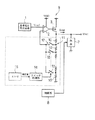
以下、本発明の一実施例について図1及び図2を参照して説明する。尚、図3及び図4と同一部分には同一符号を付して説明を省略し、以下異なる部分についてのみ説明する。本実施例における電源回路(電源回路装置)21は、図4に示す電源回路9のメモリ15をメモリ(データ記憶部)22に置き換えると共に、制御部8とメモリ22との間にアドレス発生部23を配置して構成されている。
【0016】
アドレス発生部23は、制御部(動作制御部)8によって出力されるモード切替え信号に応じて、複数のアドレスを発生させるように構成されている。メモリ22及びアドレス発生部23の構成は、直列抵抗回路11及びスイッチアレイ12の構成に応じて定められる。例えば、直列抵抗回路11における抵抗10の数が「17」であり、スイッチアレイ12におけるスイッチ13の数が「16」であれば、メモリ22の1ワードにおけるデータビット数、並びに、アドレス発生部23が発生させてメモリ22に出力するアドレスのビット数は何れも「4」となる。
【0017】
また、この場合、スイッチ制御部14は、メモリ22より出力される4ビットデータ「0000(0)」〜「1111(15)」に応じて、スイッチ13(1)〜13(16)を夫々閉路するように制御信号を出力する。
【0018】
アドレス発生部23は、制御部8が出力するモード切替え信号の状態遷移数に応じたアドレスを発生させるようになっている。例えば、状態遷移数が「3」であれば、3種類の4ビットアドレスを発生させる。また、メモリ22は、アドレスが与えられている状態ではそのアドレスに対応するメモリセルのデータを常時スイッチ制御部14に出力するように構成されている。
【0019】
尚、オペアンプ2,直列抵抗回路11及びスイッチアレイ12は、増幅回路24を構成しており、それにFET3を加えたものが電源供給部25を構成している。また、直列抵抗回路11,スイッチアレイ12,スイッチ制御部14は、増幅率切替え部26を構成しており、増幅回路24と増幅率切替え部26とは電圧変化部27を構成している。また、増幅率切替え部26にメモリ22及びアドレス発生部23を加えたものが電圧制御部28を構成している。
【0020】
図2は、電源回路21のメモリ22にデータを書き込んで設定する場合の手順を示すフローチャートである。尚、以下の作業を実行する場合、スイッチ制御部14によるスイッチアレイ12の選択は取り敢えず無効化しておく。先ず、作業者は、スイッチアレイ12の何れかのスイッチ13を閉じて電源供給部25のゲインを仮に設定する(ステップS1)。例えば、Vref=1.24V程度であり、電源Voutの電圧設定目標がVout=4.96Vであれば、直列抵抗回路11の分圧抵抗比によってゲイン(増幅率)が「4」となるスイッチ13を閉じる。
【0021】
そして、制御部8により負荷(制御対象)7を何れかの動作モードで動作させ(ステップS2)、各動作モードにおける電源Voutの電圧を測定しながらスイッチアレイ12の何れかのスイッチ13を閉じてゲインを調整する(ステップS3)。電圧Voutが適切なレベルに設定されるスイッチ13を選択すると、その動作モードに応じてアドレス発生部23が発生させるメモリ22のアドレスに対応するメモリセルに、当該スイッチ13を選択するためのデータを書き込んで記憶させる(ステップS4)。それから、全ての動作モードについて上記処理を実行した場合は(ステップS5,「YES」)処理を終了し、全ての動作モードについて実行していなければ(「NO」)ステップS1に戻る。
【0022】
一例を挙げると、制御部8により負荷7に与えられるモード切替え信号(例えば、モータである負荷7の速度指令信号)がモードA,B,Cの三種類であり、負荷7による消費電流量はモードA,B,Cの順で増加するものとする。尚、この場合、モード切替え信号は、アナログ信号でも、2ビットデータのデジタル信号でも、3本の独立した信号線で出力されるものであっても良く、信号の出力形態に応じてアドレス発生部23の入力側を適宜構成すれば良い。
【0023】
そして、各動作モードA,B,Cに応じてアドレス発生部23が発生させるアドレスが例えば「0001」,「0010」,「0100」に設定されているとする。また、電源回路21は、何れの動作モードにおいても電圧Voutが一定となる定電圧回路として構成されており、電圧Voutを一定に維持するため各モードについて選択すべきスイッチ13が(5),(8),(12)であったとすると、メモリ22には、以下のようにデータが書き込まれる。

以上のようにして、メモリ22にデータを書き込んだ後、スイッチ制御部14によるスイッチアレイ12の選択を有効化する。すると、以降は、制御部8が出力するモード切替え信号に応じてメモリ22に書き込まれたデータが読み出されてスイッチ制御部14に与えられ、前記データによって指定されるスイッチ13が閉路する。そして、電源供給部25には各動作モードで異なるゲインが設定されるようになり、電圧Voutは略一定に維持される。
【0025】
以上のように本実施例によれば、電圧制御部28は、制御部8が出力するモード切替え信号を参照して負荷7の動作モード、即ち電流消費状態がどのように変化するのかを判別し、モード切替え信号に基づいて、電源供給部25が負荷7に供給する電源Voutの電圧を制御するので、負荷7の電流消費状態が大きく変動する場合でも、前記電圧が所定の値となるように制御することができる。
【0026】
そして、電圧制御部28のアドレス発生部23は、異なるモード切替え信号に応じてアドレスを発生させてメモリ22に出力し、メモリ22がそのアドレスに対応するデータ出力すると、電圧変化部27は、与えられたデータに応じて電源Voutの電圧を変化させるので、電源Voutの電圧が、各動作モードにおいて適切なレベルとなるように広い範囲で調整することができる。
【0027】
また、電圧変化部27を、増幅回路24と増幅率切替え部26とで構成したので、メモリ22より与えられるデータに応じて増幅回路24の増幅率を複数段階に変化させて、電源Voutの電圧を調整することができる。更に、増幅率切替え部26を、直列抵抗回路11,スイッチアレイ12,スイッチ制御部14で構成したので、スイッチ制御部14は、与えられたデータに応じてスイッチアレイ12の複数のスイッチ13の内いずれかを択一的に閉路させて、電源供給部25における増幅回路24の増幅率を変化させるので、簡単な構成によって増幅率を変化させ、電圧調整を行なうことができる。
【0028】
本発明は上記しかつ図面に記載した実施例にのみ限定されるものではなく、以下のような変形または拡張が可能である。
モード切替え信号は、必ずしも動作制御部が制御対象に直接出力する信号に限らず、別途、電源回路装置用に出力する信号であっても良い。例えば、動作制御部が制御対象に直接出力する信号がアナログ信号である場合に、アドレス発生部に出力されるモード切替え信号は、そのアナログ信号の変化に応じてステップ的に変化する信号であっても良い。
また、制御対象側にもサブ制御用のマイコンなどが配置されている場合、上述したようにモード切替え信号はデジタルデータであっても良い。
アドレス発生部とデータ記憶部とを一体に構成しても良い。
電源電圧を常に一定に維持するものに限らず、制御対象の種類により動作モードに応じて電源電圧をダイナミックに変更するように設定しても良い。
制御対象は、その他、例えばスリープ/ウェイクアップ,のように動作モードが切替わるマイクロコンピュータなどでも良い。その場合、動作制御部は、外部要因に応じてマイクロコンピュータにモード切替え信号を出力する構成要素となる。要は、各種の動作モードに応じて消費電流が比較的大きな範囲で変化する制御対象に電源を供給する電源回路装置であれば適用が可能である。
【図面の簡単な説明】
【図1】本発明の一実施例であり、電源回路の電気的構成を示す機能ブロック図
【図2】電源回路のメモリにデータを書き込んで設定する場合の手順を示すフローチャート
【図3】従来技術を示す図1相当図(その1)
【図4】図1相当図(その2)
【符号の説明】
7は負荷(制御対象)、8は制御部(動作制御部)、12はスイッチアレイ、14はスイッチ制御部、21は電源回路(電源回路装置)、22はメモリ(データ記憶部)、23はアドレス発生部、24は増幅回路、25は電源供給部、26は増幅率切替え部、27は電圧変化部、28は電圧制御部を示す。[0001]
TECHNICAL FIELD OF THE INVENTION
The present invention relates to a power supply circuit device that controls a voltage of a power supply generated by a power supply unit based on a reference voltage generated by a reference voltage generation circuit.
[0002]
[Prior art]
FIG. 3 shows a conventional example of a power supply circuit that generates a power supply of a predetermined voltage using a reference voltage generation circuit. The reference
[0003]
The drain of the FET 3 supplies an operating power of a voltage Vout to the
Vout = Vref × (R1 + R2) / R2
Iout is an output current of the
[0004]
In the
[0005]
FIG. 4 shows a
[0006]
Only one of the
[0007]
Then, for example, the operator measures the voltage Vout output from the
[0008]
[Problems to be solved by the invention]
In the
[0009]
The present invention has been made in view of the above circumstances, and an object of the present invention is to provide a power supply circuit device that can adjust a power supply voltage according to a change even when a current consumption state of a load greatly changes. It is in.
[0010]
[Means for Solving the Problems]
According to the power supply circuit device of the first aspect, the voltage control unit refers to the mode switching signal that is output by the operation control unit to switch the operation mode of the control target. It is possible to determine how the state changes. Therefore, by controlling the voltage of the power supply supplied to the control target by the power supply unit based on the mode switching signal, even if the current consumption state of the control target greatly fluctuates, the voltage is set to a predetermined value. Can be controlled.
[0011]
According to the power supply circuit device of the second aspect, the address generation unit of the voltage control unit generates a different address according to the output state of the mode switching signal, and outputs the generated address to the data storage unit. Then, the data stored at the address is read from the data storage unit and applied to the voltage change unit, and the voltage change unit changes the power supply voltage according to the applied data.
[0012]
That is, the operator makes the following settings in advance. First, power is supplied to the control target from the power supply unit in a state where the power supply voltage level in the voltage change unit is appropriately set, and the power supply voltage when the operation mode of the control target changes is measured. Then, the voltage setting in the voltage changing unit is changed while observing the power supply voltage to be at an appropriate level in each operation mode. When the voltage setting is determined, voltage setting data is written and stored in the address of the data storage unit generated by the address generation unit according to each operation mode.
By storing data in the data storage unit as described above, the voltage of the power supply supplied from the power supply unit to the control target can be adjusted in a wide range so as to be at an appropriate level in each operation mode. it can.
[0013]
According to the power supply circuit device of the third aspect, since the voltage changing unit is constituted by the amplification circuit for amplifying the reference voltage and the amplification factor switching unit, the amplification factor of the amplification circuit according to the data provided from the data storage unit. Can be changed in a plurality of stages to adjust the power supply voltage.
[0014]
According to the power supply circuit device of the fourth aspect, the switch control unit selectively closes one of the plurality of switches of the switch array in accordance with the data provided from the data storage unit. Then, the connection state between the resistor in the series resistor circuit and the amplifier circuit changes according to the closed switch, so that the amplification factor of the amplifier circuit changes. Therefore, the amplification factor can be changed by a simple configuration.
[0015]
BEST MODE FOR CARRYING OUT THE INVENTION
Hereinafter, an embodiment of the present invention will be described with reference to FIGS. The same parts as those in FIGS. 3 and 4 are denoted by the same reference numerals, and the description thereof will be omitted. The power supply circuit (power supply circuit device) 21 according to the present embodiment replaces the
[0016]
The address generator 23 is configured to generate a plurality of addresses according to a mode switching signal output by the controller (operation controller) 8. The configurations of the memory 22 and the address generator 23 are determined according to the configurations of the
[0017]
In this case, the
[0018]
The address generator 23 generates an address corresponding to the number of state transitions of the mode switching signal output by the
[0019]
The
[0020]
FIG. 2 is a flowchart showing a procedure for writing and setting data in the memory 22 of the power supply circuit 21. When performing the following operations, the selection of the
[0021]
Then, the
[0022]
For example, mode switching signals (for example, a speed command signal of the
[0023]
It is assumed that the addresses generated by the address generation unit 23 according to the operation modes A, B, and C are set to, for example, “0001”, “0010”, and “0100”. Further, the power supply circuit 21 is configured as a constant voltage circuit in which the voltage Vout is constant in any operation mode, and the
After writing data in the memory 22 as described above, the selection of the
[0025]
As described above, according to the present embodiment, the voltage control unit 28 determines how the operation mode of the
[0026]
Then, the address generator 23 of the voltage controller 28 generates an address in response to a different mode switching signal and outputs the generated address to the memory 22, and when the memory 22 outputs data corresponding to the address, the
[0027]
Further, since the
[0028]
The present invention is not limited to the embodiment described above and shown in the drawings, and the following modifications or extensions are possible.
The mode switching signal is not necessarily a signal that is directly output to the control target by the operation control unit, and may be a signal that is separately output for the power supply circuit device. For example, when the signal output directly to the control target by the operation control unit is an analog signal, the mode switching signal output to the address generation unit is a signal that changes stepwise according to the change of the analog signal. Is also good.
When a sub-control microcomputer or the like is also provided on the control target side, the mode switching signal may be digital data as described above.
The address generation unit and the data storage unit may be configured integrally.
The power supply voltage is not limited to always being kept constant, and the power supply voltage may be dynamically changed depending on the operation mode depending on the type of the control target.
The control target may also be a microcomputer or the like whose operation mode is switched, such as sleep / wakeup. In this case, the operation control unit is a component that outputs a mode switching signal to the microcomputer according to an external factor. In short, the present invention can be applied to any power supply circuit device that supplies power to a control target whose current consumption changes in a relatively large range according to various operation modes.
[Brief description of the drawings]
FIG. 1 is a functional block diagram showing an electric configuration of a power supply circuit according to an embodiment of the present invention. FIG. 2 is a flowchart showing a procedure for writing data in a memory of the power supply circuit and setting the data. Fig. 1 equivalent diagram showing technology (1)
FIG. 4 is a diagram corresponding to FIG. 1 (part 2);
[Explanation of symbols]
7 is a load (control target), 8 is a control unit (operation control unit), 12 is a switch array, 14 is a switch control unit, 21 is a power supply circuit (power supply circuit device), 22 is a memory (data storage unit), and 23 is An address generation unit, 24 is an amplification circuit, 25 is a power supply unit, 26 is an amplification rate switching unit, 27 is a voltage change unit, and 28 is a voltage control unit.
Claims (4)
この基準電圧発生回路によって発生される基準電圧に基づき所定電圧の電源を生成して供給する電源供給部と、
動作制御部が制御対象の動作モードを切替えることに伴って出力されるモード切替え信号を受けて、前記電源供給部により前記制御対象に供給される電源の電圧が当該制御対象の動作モードに応じた適切なレベルとなるように制御する電圧制御部とで構成されることを特徴とする電源回路装置。A reference voltage generating circuit;
A power supply unit for generating and supplying power of a predetermined voltage based on a reference voltage generated by the reference voltage generation circuit;
When the operation control unit receives a mode switching signal output in accordance with switching the operation mode of the control target, the voltage of the power supplied to the control target by the power supply unit corresponds to the operation mode of the control target. A power supply circuit device, comprising: a voltage control unit that controls an appropriate level.
前記モード切替え信号の出力状態に応じて異なるアドレスを発生させるアドレス発生部と、
前記アドレスが与えられると、そのアドレスに記憶されているデータが読み出されるデータ記憶部と、
このデータ記憶部より読み出されたデータに応じて電源電圧を変化させる電圧変化部とで構成されていることを特徴とする請求項1記載の電源回路装置。The voltage control unit includes:
An address generation unit that generates different addresses according to the output state of the mode switching signal;
Given the address, a data storage unit from which data stored at the address is read;
2. The power supply circuit device according to claim 1, further comprising a voltage change unit that changes a power supply voltage in accordance with the data read from the data storage unit.
前記基準電圧を増幅する増幅回路と、
この増幅回路の増幅率を複数段階に切替えるように構成される増幅率切替え部とで構成されていることを特徴とする請求項2記載の電源回路装置。The voltage changing unit includes:
An amplifier circuit for amplifying the reference voltage;
3. The power supply circuit device according to claim 2, further comprising an amplification factor switching unit configured to switch an amplification factor of the amplification circuit in a plurality of stages.
前記増幅回路の増幅率を設定するための複数の抵抗を直列接続してなる直列抵抗回路と、
この直列抵抗回路の各共通接続点と前記増幅回路の入力端子との間に接続される複数のスイッチよりなるスイッチアレイと、
前記データ記憶部より読み出されたデータに応じて前記スイッチアレイを構成するスイッチの内何れかを択一的に閉路するスイッチ制御部とで構成されることを特徴とする請求項3記載の電源回路装置。The amplification factor switching unit,
A series resistor circuit in which a plurality of resistors for setting the amplification factor of the amplifier circuit are connected in series;
A switch array including a plurality of switches connected between each common connection point of the series resistance circuit and an input terminal of the amplification circuit;
4. The power supply according to claim 3, further comprising a switch control unit that selectively closes one of the switches constituting the switch array in accordance with the data read from the data storage unit. Circuit device.
Priority Applications (1)
| Application Number | Priority Date | Filing Date | Title |
|---|---|---|---|
| JP2002310980A JP4052088B2 (en) | 2002-10-25 | 2002-10-25 | Power circuit equipment |
Applications Claiming Priority (1)
| Application Number | Priority Date | Filing Date | Title |
|---|---|---|---|
| JP2002310980A JP4052088B2 (en) | 2002-10-25 | 2002-10-25 | Power circuit equipment |
Publications (2)
| Publication Number | Publication Date |
|---|---|
| JP2004145703A true JP2004145703A (en) | 2004-05-20 |
| JP4052088B2 JP4052088B2 (en) | 2008-02-27 |
Family
ID=32456342
Family Applications (1)
| Application Number | Title | Priority Date | Filing Date |
|---|---|---|---|
| JP2002310980A Expired - Fee Related JP4052088B2 (en) | 2002-10-25 | 2002-10-25 | Power circuit equipment |
Country Status (1)
| Country | Link |
|---|---|
| JP (1) | JP4052088B2 (en) |
Cited By (4)
| Publication number | Priority date | Publication date | Assignee | Title |
|---|---|---|---|---|
| JP2006293802A (en) * | 2005-04-13 | 2006-10-26 | Renesas Technology Corp | Semiconductor integrated circuit device |
| JP2008070977A (en) * | 2006-09-12 | 2008-03-27 | Fujitsu Ltd | Power-supply voltage step-down circuit and semiconductor device |
| KR101412450B1 (en) | 2006-06-26 | 2014-06-30 | 세미컨덕터 콤포넨츠 인더스트리즈 엘엘씨 | Method of forming a programmable voltage regulator and structure therefor |
| CN111124026A (en) * | 2019-12-31 | 2020-05-08 | 龙迅半导体(合肥)股份有限公司 | Data switch and data transmission system |
-
2002
- 2002-10-25 JP JP2002310980A patent/JP4052088B2/en not_active Expired - Fee Related
Cited By (6)
| Publication number | Priority date | Publication date | Assignee | Title |
|---|---|---|---|---|
| JP2006293802A (en) * | 2005-04-13 | 2006-10-26 | Renesas Technology Corp | Semiconductor integrated circuit device |
| JP4711287B2 (en) * | 2005-04-13 | 2011-06-29 | ルネサスエレクトロニクス株式会社 | Semiconductor integrated circuit device |
| KR101412450B1 (en) | 2006-06-26 | 2014-06-30 | 세미컨덕터 콤포넨츠 인더스트리즈 엘엘씨 | Method of forming a programmable voltage regulator and structure therefor |
| JP2008070977A (en) * | 2006-09-12 | 2008-03-27 | Fujitsu Ltd | Power-supply voltage step-down circuit and semiconductor device |
| CN111124026A (en) * | 2019-12-31 | 2020-05-08 | 龙迅半导体(合肥)股份有限公司 | Data switch and data transmission system |
| CN111124026B (en) * | 2019-12-31 | 2021-09-03 | 龙迅半导体(合肥)股份有限公司 | Data switch and data transmission system |
Also Published As
| Publication number | Publication date |
|---|---|
| JP4052088B2 (en) | 2008-02-27 |
Similar Documents
| Publication | Publication Date | Title |
|---|---|---|
| US9165666B2 (en) | Charge pump apparatus, a memory integrated circuit and methods of power supply | |
| JP4855664B2 (en) | Temperature sensor for sensing temperature and outputting corresponding digital data, and LCD driving integrated circuit having the same | |
| JP4285506B2 (en) | Auto gain control circuit | |
| JP4792034B2 (en) | Semiconductor device and control method thereof | |
| JP2006191359A (en) | Voltage supply circuit, microphone unit and method of adjusting sensitivity of unit | |
| KR100706239B1 (en) | Voltage regulator capable of decreasing power consumption at standby mode | |
| JP4274786B2 (en) | Voltage generation circuit | |
| KR101411977B1 (en) | Voltage regulator, flash memory device having its and memory system having its | |
| JP4654765B2 (en) | Load driving device and output adjusting method of load driving device | |
| GB2364402A (en) | Regulated Buzzer Drive Circuit | |
| US20140375130A1 (en) | Circuit, Use, and Method for Operating a Circuit | |
| JP4764996B2 (en) | Semiconductor physical quantity sensor device | |
| JP2004145703A (en) | Power circuit device | |
| KR100550790B1 (en) | Drain pump for a flash memory | |
| JP4626503B2 (en) | Operational amplifier circuit | |
| JP2014147044A (en) | Semiconductor integrated circuit | |
| WO2006042058A2 (en) | Memory regulator system with test mode | |
| JP4465330B2 (en) | Operation control method of stabilized power supply circuit | |
| JP2003302301A (en) | Semiconductor physical quantity sensor apparatus | |
| JP4758306B2 (en) | Auto range current mirror circuit | |
| KR100206705B1 (en) | External supply voltage sensing circuit of semiconductor memory device | |
| KR20090010429A (en) | Internal voltage generator of semiconductor memory device | |
| JP2000122738A (en) | Current source circuit and voltage generating circuit | |
| JP7175867B2 (en) | Current detection device and data writing method | |
| JP2008027141A (en) | Constant-voltage circuit |
Legal Events
| Date | Code | Title | Description |
|---|---|---|---|
| A621 | Written request for application examination |
Free format text: JAPANESE INTERMEDIATE CODE: A621 Effective date: 20041206 |
|
| A977 | Report on retrieval |
Free format text: JAPANESE INTERMEDIATE CODE: A971007 Effective date: 20070425 |
|
| A131 | Notification of reasons for refusal |
Free format text: JAPANESE INTERMEDIATE CODE: A131 Effective date: 20070515 |
|
| A521 | Written amendment |
Free format text: JAPANESE INTERMEDIATE CODE: A523 Effective date: 20070705 |
|
| A131 | Notification of reasons for refusal |
Free format text: JAPANESE INTERMEDIATE CODE: A131 Effective date: 20070821 |
|
| A521 | Written amendment |
Free format text: JAPANESE INTERMEDIATE CODE: A523 Effective date: 20071009 |
|
| TRDD | Decision of grant or rejection written | ||
| A01 | Written decision to grant a patent or to grant a registration (utility model) |
Free format text: JAPANESE INTERMEDIATE CODE: A01 Effective date: 20071113 |
|
| A61 | First payment of annual fees (during grant procedure) |
Free format text: JAPANESE INTERMEDIATE CODE: A61 Effective date: 20071126 |
|
| FPAY | Renewal fee payment (event date is renewal date of database) |
Free format text: PAYMENT UNTIL: 20101214 Year of fee payment: 3 |
|
| R150 | Certificate of patent (=grant) or registration of utility model |
Free format text: JAPANESE INTERMEDIATE CODE: R150 |
|
| FPAY | Renewal fee payment (event date is renewal date of database) |
Free format text: PAYMENT UNTIL: 20111214 Year of fee payment: 4 |
|
| FPAY | Renewal fee payment (event date is renewal date of database) |
Free format text: PAYMENT UNTIL: 20121214 Year of fee payment: 5 |
|
| FPAY | Renewal fee payment (event date is renewal date of database) |
Free format text: PAYMENT UNTIL: 20131214 Year of fee payment: 6 |
|
| R250 | Receipt of annual fees |
Free format text: JAPANESE INTERMEDIATE CODE: R250 |
|
| LAPS | Cancellation because of no payment of annual fees |