JP2004145279A - Electronic circuit, method for driving electronic circuit, electrooptical device, method for driving electrooptical device, and electronic apparatus - Google Patents
Electronic circuit, method for driving electronic circuit, electrooptical device, method for driving electrooptical device, and electronic apparatus Download PDFInfo
- Publication number
- JP2004145279A JP2004145279A JP2003207374A JP2003207374A JP2004145279A JP 2004145279 A JP2004145279 A JP 2004145279A JP 2003207374 A JP2003207374 A JP 2003207374A JP 2003207374 A JP2003207374 A JP 2003207374A JP 2004145279 A JP2004145279 A JP 2004145279A
- Authority
- JP
- Japan
- Prior art keywords
- terminal
- transistor
- unit circuits
- power supply
- supply line
- Prior art date
- Legal status (The legal status is an assumption and is not a legal conclusion. Google has not performed a legal analysis and makes no representation as to the accuracy of the status listed.)
- Withdrawn
Links
- 238000000034 method Methods 0.000 title claims abstract description 36
- 239000003990 capacitor Substances 0.000 claims description 39
- 239000011159 matrix material Substances 0.000 abstract description 18
- 238000010586 diagram Methods 0.000 description 12
- 230000007274 generation of a signal involved in cell-cell signaling Effects 0.000 description 10
- 230000000694 effects Effects 0.000 description 3
- 238000004519 manufacturing process Methods 0.000 description 3
- 230000006870 function Effects 0.000 description 2
- 230000001413 cellular effect Effects 0.000 description 1
- 239000011368 organic material Substances 0.000 description 1
- 230000004044 response Effects 0.000 description 1
- 239000004065 semiconductor Substances 0.000 description 1
- 239000010409 thin film Substances 0.000 description 1
Images


Abstract
Description
【0001】
【発明の属する技術分野】
本発明は、電子回路、電子回路の駆動方法、電気光学装置、電気光学装置の駆動方法及び電子機器に関するものである。
【0002】
【従来の技術】
近年、広く表示装置として用いられる複数の電気光学素子を備えた電気光学装置は、高精彩化あるいは大画面化が求められており、これに呼応して、複数の電気光学素子の各々を駆動するための画素回路を備えたアクティブマトリクス駆動型電気光学装置のパッシブ駆動型電気光学装置に対する比重はより高まっている。しかしながら、より一層の高精彩化あるいは大画面化を達成するためには、電気光学素子をそれぞれ精密に制御する必要がある。そのためには、画素回路を構成する能動素子の特性バラツキを補償しなければならない。
【0003】
能動素子の特性バラツキの補償方法として、例えば、特性バラツキを補償するための、ダイオード接続したトランジスタを含む画素回路を備えた表示装置(例えば、特許文献1を参照)が提案されている。
【0004】
【特許文献1】特開平11−272233号公報
【0005】
【発明が解決しようとする課題】
ところで、能動素子の特性バラツキを補償する画素回路は、一般に4つ以上のトランジスタにより構成され、そのため、歩留まりや開口率の低下を招くこととなる。
【0006】
本発明の一つの目的は、上記問題点を解消することであって、画素回路、あるいは単位回路を構成するトランジスタの個数を削減することができる電子回路、電子回路の駆動方法、電気光学装置、電気光学装置の駆動方法及び電子機器を提供することにある。
【0007】
【課題を解決するための手段】
本発明の第1の電子回路は、複数の単位回路を含む電子回路であって、第1の電源線を含み、前記複数の単位回路の各々は、電子素子に直列に接続されるともに前記第1の電源線に接続された第1のトランジスタと、前記第1のトランジスタのドレインと前記第1のトランジスタのゲートとの導通を制御する第2のトランジスタと、前記第1のトランジスタの導通状態を設定するためのデータ電流を出力する電流源と前記第1のトランジスタとの導通を制御する第3のトランジスタと、を備え、前記第3のトランジスタがオン状態にある期間のうち少なくとも1部の期間において、前記第1の電源線は駆動電圧から電気的に切断され、前記第3のトランジスタがオフ状態にある期間のうち少なくとも1部の期間において、前記第1の電源線と前記電子素子との間に、前記第1のトランジスタに前記データ電流により設定された前記第1のトランジスタの導通状態に応じた電流が流れることを特徴とする。
上記の電子回路において、「前記第1のトランジスタのドレインと前記第1のトランジスタのゲートとの導通を制御する」とは、前記第1のトランジスタの前記ドレインと前記第1のトランジスタの前記ゲートとを直接電気的に接続する場合ばかりではなく、前記第3のトランジスタなど、他のトランジスタなどの素子、あるいは配線を介して電気的に接続する場合も含む。
【0008】
本発明の第2の電子回路は、複数の単位回路を含む電子回路であって、第1の電源線と、前記第1の電源線の電位を複数の電位に設定する、あるいは、前記第1の電源線への駆動電圧の供給及び遮断を制御する制御回路と、を含み、前記複数の単位回路の各々は、電子素子と、前記電子素子に直列に接続されるともに前記第1の電源線に接続された第1のトランジスタと、前記第1のトランジスタのドレインと前記第1のトランジスタとのゲートとの導通を制御する第2のトランジスタと、前記第1のトランジスタの導通状態を設定するためのデータ電流を出力する電流源と前記第1のトランジスタとの導通を制御する第3のトランジスタと、を備え、前記第3のトランジスタがオフ状態にある期間のうち少なくとも1部の期間において、前記第1の電源線と前記電子素子との間に、前記第1のトランジスタに前記データ電流により設定された前記第1のトランジスタの導通状態に応じた電流が流れることを特徴とする。
【0009】
上記の電子回路において、「ドレイン」はデータ電流が前記第1のトランジスタを流れる際の前記第1のトランジスタのチャネルを挟む2つの端子の電位の相対的な関係と前記第1のトランジスタの導電型によって決定される。例えば、前記第1のトランジスタがp型である場合は、前記第1のトランジスタの前記2つの端子のうち電位が低い端子を「ドレイン」と言い、前記第1のトランジスタがn型である場合は、前記第1のトランジスタの前記2つの端子のうち電位が高い端子を「ドレイン」と言う。
上記の電子回路において、「電子素子」とは、例えば、電気光学素子、抵抗素子、ダイオード等である。
【0010】
本発明における第3の電子回路は、複数の単位回路を含む電子回路であって、前記複数の単位回路の各々は、第1の端子と第2の端子と第1の制御用端子とを有する第1のトランジスタと、第3の端子と第4の端子とを有し、前記第1の制御用端子に前記第3の端子が接続され、前記2の端子と前記第3の端子との電気的接続を制御する第2のトランジスタと、第5の端子と第6の端子とを有し、前記第1の端子に前記第5の端子が接続された第3のトランジスタと、第7の端子と第8の端子とを有し、前記第7の端子が前記第1の制御用端子及び前記第3の端子に接続された容量素子と、を含み、前記第1の端子は前記複数の単位回路の他の単位回路の前記第1の端子と共に第1の電源線に接続され、前記第1の電源線の電位を複数の電位に設定する、あるいは、前記第1の電源線への駆動電圧の供給及び遮断を制御する制御回路を備えている。
【0011】
上記の第1のトランジスタ、第1の端子、第2の端子及び第1の制御用端子は、例えば、後述する実施形態の図3の画素回路においては、駆動トランジスタQ1、駆動トランジスタQ1のソース、駆動トランジスタQ1のドレイン、駆動トランジスタQ1のゲートに対応している。
【0012】
また、第2のトランジスタ、第3の端子、第4の端子及び第2の制御用端子は、それぞれ、トランジスタQ2、トランジスタQ2のソース、トランジスタQ2のドレイン、トランジスタQ2のゲートに対応している。
さらに、第3のトランジスタ、第5の端子、第6の端子、第3の制御用端子は、それぞれ、スイッチングトランジスタQ3、スイッチングトランジスタQ3のソース、スイッチングトランジスタQ3のドレイン、スイッチングトランジスタQ3のゲートに対応している。
また、容量素子、第7の端子及び第8の端子は、それぞれ、保持用キャパシタCo、保持用キャパシタCoの第1の電極La及び保持用キャパシタCoの第2の電極Lbに対応している。
これによれば、従来のものと比べて使用するトランジスタの数を削減された単位回路を構成することができる。
【0013】
本発明における第4の電子回路は、複数の単位回路を含む電子回路であって、前記複数の単位回路の各々は、第1の端子と第2の端子と第1の制御用端子とを有する第1のトランジスタと、第3の端子と第4の端子とを有し、前記第1の制御用端子に前記第3の端子が接続され、前記2の端子と前記第4の端子との電気的接続を制御する第2のトランジスタと、第5の端子と第6の端子とを有し、前記第1の端子に前記第5の端子が接続された第3のトランジスタと、第7の端子と第8の端子とを有し、前記第7の端子が前記第1の制御用端子及び前記第3の端子に接続された容量素子と、を含み、前記第1の端子は前記複数の単位回路の他の単位回路の前記第1の端子と共に第1の電源線に接続され、前記第8の端子は前記複数の単位回路の他の単位回路の前記第8の端子と共に所定電位に保持された第2の電源線に接続され、前記第1の電源線の電位を複数の電位に設定する、あるいは、前記第1の電源線への駆動電圧の供給及び遮断を制御する制御回路を備えている。
これによれば、従来のものと比べて使用するトランジスタの数を削減して単位回路を構成することができることに加えて、容量素子に電圧を安定して保持させることができる。
【0014】
上記の電子回路において、前記単位回路の各々に含まれるトランジスタは、前記第1のトランジスタ、前記第2のトランジスタ及び前記第3のトランジスタのみである。
これによれば、使用するトランジスタの数を従来のものに比べて1つ削減して単位回路を構成することができる。
上記の電子回路において、前記第2の端子には電子素子が接続されている。
これによれば、従来のものと比べて使用するトランジスタが1つ少ない回路で電子素子を制御することができる。
上記の電子回路において、前記電子素子は電流駆動素子であってもよい。
これによれば、従来のものと比べて使用するトランジスタが1つ少ない回路で電流駆動素子を制御することができる。
上記の電子回路において、前記制御回路は第9の端子と第10の端子とを備えた第4のトランジスタであり、前記第9の端子は前記駆動電圧に接続され、前記第10の端子は前記第1の電源線に接続されていてもよい。
これによれば、制御回路を容易に構成することができる。
【0015】
本発明の第1の電子回路の駆動方法は、複数の単位回路を含む電子回路の駆動方法であって、前記電子回路は、第1の電源線を含み、前記複数の単位回路の各々は、電子素子に直列に接続されるともに前記第1の電源線に接続された第1のトランジスタと、前記第1のトランジスタのドレインと前記第1のトランジスタとのゲートとの導通を制御する第2のトランジスタと、前記第1のトランジスタの導通状態を設定するためのデータ電流を出力する電流源と前記第1のトランジスタとの導通を制御する第3のトランジスタと、を備え、前記第3のトランジスタをオン状態として前記データ電流を前記第1のトランジスタに供給し、前記第1のトランジスタの導通状態を設定する第1のステップと、前記第3のトランジスタをオフ状態とし、前記第1の電源線と前記電子素子との間に前記第1のトランジスタの前記導通状態に応じた電流を流す第2のステップと、を含み、前記第1のステップの前記データ電流を前記第1のトランジスタに供給する期間の少なくとも1部の期間において、前記第1の電源線を駆動電圧から電気的に切り離し、前記第2のステップを行っている期間の少なくとも1部の期間において、前記第1のトランジスタの前記ドレイン及びソースのいずれか一方に前記第1の電源線を介して前記駆動電圧を印加すること、を特徴とする。
【0016】
本発明の第2の電子回路の駆動方法は、第1の端子と第2の端子と第1の制御用端子とを有する第1のトランジスタと、第3の端子と第4の端子とを有し、前記第1の制御用端子に前記第3の端子が接続され、前記第2の端子に前記第4の端子が接続された第2のトランジスタと、第5の端子と第6の端子とを有し、前記第1の端子に前記第5の端子が接続された第3のトランジスタと、第7の端子及び第8の端子を有し、前記第7の端子が前記第1の制御用端子及び前記第3の端子に接続された容量素子と、を含む単位回路を複数備え、前記第1の端子は前記複数の単位回路のうちの一連の単位回路の前記第1の端子と共に第1の電源線に接続されている電子回路の駆動方法であって、前記第1の電源線を駆動電圧から電気的に切り離すことにより、前記一連の単位回路の前記第1の端子を前記駆動電圧から電気的に切り離し、かつ、前記一連の単位回路の前記第3のトランジスタをオン状態とすることにより、前記第1のトランジスタを経由して流れる電流の電流レベルに応じた電荷量を前記容量素子に保持し、前記電荷量に応じた電圧を前記第1の制御用端子に印加して、前記第1の端子と前記第2の端子との間の導通状態を設定するステップと、前記第3のトランジスタをオフ状態にするとともに、前記一連の単位回路の前記第1の端子を前記駆動電圧に電気的に接続にするステップと、を含む。
【0017】
本発明の第3電子回路の駆動方法は、第1の端子と第2の端子と第1の制御用端子とを有する第1のトランジスタと、第3の端子と第4の端子とを有し、前記第1の制御用端子に前記第3の端子が接続され、前記第2の端子に前記第4の端子が接続された第2のトランジスタと、第5の端子と第6の端子とを有し、前記第1の端子に前記第5の端子が接続された第3のトランジスタと、第7の端子及び第8の端子を有し、前記第7の端子が前記第1の制御用端子及び前記第3の端子に接続された容量素子と、を含む単位回路を複数備え、前記第1の端子は前記複数の単位回路のうちの一連の単位回路の前記第1の端子と共に第1の電源線に接続されるとともに、前記第8の端子は前記複数の単位回路のうちの一連の単位回路の前記第8の端子と共に第2の電源線に接続されている電子回路の駆動方法であって、前記第1の電源線を駆動電圧から電気的に切り離すことにより、前記一連の単位回路の前記第1の端子を前記駆動電圧から電気的に切り離し、かつ、前記一連の単位回路の前記第3のトランジスタがオン状態とすることにより、前記第1のトランジスタを経由して流れる電流の電流レベルに応じた電荷量を前記容量素子に保持し、前記電荷量に応じた電圧を前記第1の制御用端子に印加して、前記第1の端子と前記第2の端子との間の導通状態を設定するステップと、前記第3のトランジスタをオフ状態にするとともに、前記一連の単位回路の前記第1の端子を前記駆動電圧に電気的に接続するステップとを含む。
上記の電子回路の駆動方法によれば、前記単位回路内のトランジスタ数を可能な限り少なくすることができる。
【0018】
本発明の第1の電気光学装置は、複数の走査線と、複数のデータ線と、複数の第1の電源線と、複数の単位回路と、を含み、前記複数の単位回路の各々は、電気光学素子に直列に接続されるともに前記第1の電源線のうち対応する第1の電源線に接続された第1のトランジスタと、前記第1のトランジスタのドレインと前記第1のトランジスタとのゲートとの導通を制御する第2のトランジスタと、前記第1のトランジスタと前記複数のデータ線のうち対応するデータ線との導通を制御し、前記複数の走査線のうち対応する走査線を介して供給される走査信号により制御される第3のトランジスタと、を備え、前記第3のトランジスタがオン状態にある期間のうち少なくとも1部の期間において、前記対応する第1の電源線は駆動電圧から電気的に切り離されるとともに、前記対応するデータ線から供給されるデータ電流が前記第1のトランジスタに流れることにより前記第1のトランジスタの導通状態が設定され、前記第3のトランジスタがオフ状態にある期間のうち少なくとも1部の期間において、前記第1のトランジスタの前記ドレイン及びソースのうちいずれか一方に前記駆動電圧が印加され、前記対応する第1の電源線と前記電気光学素子との間に、前記データ電流により設定された前記第1のトランジスタの前記導通状態に応じた電流が流れること、を特徴とする。
【0019】
上記の電気光学装置において、「前記第1のトランジスタのドレインと前記第1のトランジスタのゲートとの導通を制御する」とは、前記第1のトランジスタの前記ドレインと前記第1のトランジスタの前記ゲートとを直接電気的に接続する場合ばかりではなく、前記第3のトランジスタなど、他のトランジスタなどの素子、あるいは前記対応するデータ線などの配線を介して電気的に接続する場合も含む。
【0020】
本発明の第2の電気光学装置は、複数の走査線と、複数のデータ線と、複数の単位回路と、を備えた電気光学装置であって、前記複数の単位回路の各々は、第1の端子と第2の端子と第1の制御用端子とを有する第1のトランジスタと、第3の端子と第4の端子と第2の制御用端子とを有し、前記第1の制御用端子に前記第3の端子が接続された第2のトランジスタと、第5の端子と第6の端子と第3の制御用端子とを有し、前記第5の端子が前記第1の端子に接続され、前記第6の端子が前記複数のデータ線のうちの一つのデータ線に接続され、前記第3の制御用端子が複数の走査線のうちの一つの走査線に接続された第3のトランジスタと、第7の端子と第8の端子とを有し、前記第7の端子が前記第1の制御用端子及び前記第3の端子に接続された容量素子と、を含み、前記第1の端子は前記複数の単位回路の他の単位回路の前記第1の端子と共に第1の電源線に接続され、前記第1の電源線の電位を複数の電位に設定する、あるいは、前記電源線への駆動電圧の供給及び遮断を制御する制御回路を備えている。
【0021】
本発明の第3の電気光学装置は、複数の走査線と、複数のデータ線と、複数の単位回路と、を備えた電気光学装置であって、前記複数の単位回路の各々は、第1の端子と第2の端子と第1の制御用端子とを有する第1のトランジスタと、第3の端子と第4の端子と第2の制御用端子とを有し、前記第1の制御用端子に前記第3の端子が接続され、前記2の端子と前記第4の端子との電気的接続を制御する第2のトランジスタと、第5の端子と第6の端子と第3の制御用端子とを有し、前記第1の端子に前記第5の端子が接続され、前記第6の端子が前記複数のデータ線のうちの一つのデータ線に接続され、前記第3の制御用端子が複数の走査線のうちの一つの走査線に接続された第3のトランジスタと、第7の端子と第8の端子とを有し、前記第7の端子が前記第1の制御用端子及び前記第3の端子に接続された容量素子と、を含み、前記第1の端子は前記複数の単位回路の他の単位回路の前記第1の端子と共に第1の電源線に接続され、前記第8の端子は前記複数の単位回路の他の単位回路の前記第8の端子と共に所定電位に保持された第2の電源線に接続され、前記第1の電源線の電位を複数の電位に設定する、あるいは、前記第1の電源線への駆動電圧の供給及び遮断を制御する制御回路を備えている。
上記の電気光学装置においては、前記単位回路内のトランジスタ数を可能な限り少なくすることができる。
【0022】
上記の電気光学装置において、前記単位回路の各々に含まれるトランジスタは、前記第1のトランジスタ、前記第2のトランジスタ及び前記第3のトランジスタのみであることが好ましい。
【0023】
上記の電気光学装置において、前記制御回路は第9の端子と第10の端子とを備えた第4のトランジスタであり、前記第9の端子は前記駆動電圧に接続され、前記第10の端子は前記第1の電源線に接続されていることが好ましい。
【0024】
これによれば、制御回路を容易に構成することができる。
上記の電気光学装置において、前記電気光学素子は、例えば、EL素子であってもよい。中でも有機EL素子などの電流駆動素子が好適である。
【0025】
本発明の第1の電気光学装置の駆動方法は、電気光学装置の駆動方法であって、前記電気光学装置は、複数の走査線と、複数のデータ線と、複数の第1の電源線と、複数の単位回路と、を含み、前記複数の単位回路の各々は、電気光学素子に直列に接続されるともに前記第1の電源線のうち対応する第1の電源線に接続された第1のトランジスタと、前記第1のトランジスタの前記ドレインと前記第1のトランジスタとのゲートとの導通を制御する第2のトランジスタと、前記第1のトランジスタと前記複数のデータ線のうち対応するデータ線との導通を制御し、前記複数の走査線のうち対応する走査線を介して供給される走査信号により制御される第3のトランジスタと、を備え、前記第3のトランジスタがオン状態及び前記対応する第1の電源線が駆動電圧から電気的に切り離された状態で、前記対応するデータ線から供給されるデータ電流を前記第1のトランジスタに流すことにより、前記第1のトランジスタの導通状態を設定する第1のステップと、前記第3のトランジスタがオフ状態及び前記第1のトランジスタの前記ドレイン及びソースのうちいずれか一方に前記対応する第1の電源線を介して前記駆動電圧が印加された状態で、前記対応する第1の電源線と前記電気光学素子との間に、前記データ電流により設定された前記第1のトランジスタの前記導通状態に応じた電流を流す第2のステップを含むこと、を特徴とする。
【0026】
本発明の第2の電気光学装置の駆動方法は、第1の端子と第2の端子と第1の制御用端子とを有する第1のトランジスタと、第3の端子と第4の端子と第2の制御用端子とを有し、前記第1の制御用端子に前記第3の端子が接続され、前記第2の端子に前記第4の端子が接続された第2のトランジスタと、第5の端子と第6の端子と第3の制御用端子とを有し、前記第1の端子に前記第5の端子が接続された第3のトランジスタと、第7の端子と第8の端子を有し、前記第7の端子が前記第1の制御用端子及び前記第3の端子に接続された容量素子と、前記第2の端子に接続された電気光学素子と、含む単位回路を複数備え、前記第6の端子が複数のデータ線のうち1つのデータ線と接続され、前記第3の制御用端子が複数の走査線のうち1つの走査線と接続され、前記第1の端子は前記複数の単位回路の他の単位回路の前記第1の端子と共に第1の電源線に接続されている電気光学装置の駆動方法であって、前記第1の電源線を駆動電圧から電気的に切り離すことにより、前記一連の単位回路の前記第1の端子を、前記駆動電圧から電気的に切り離し、かつ、前記一連の単位回路の前記第3のトランジスタがオン状態とすることにより、前記第1のトランジスタを経由して流れる電流の電流レベルに応じた電荷量を前記容量素子に保持し、前記電荷量に応じた電圧を前記第1の制御用端子に印加して、前記第1の端子と前記第2の端子との間の導通状態を設定するステップと、前記第3のトランジスタをオフ状態にするとともに、前記一連の単位回路の前記第1の端子を前記第1の電源線を介して前記駆動電圧に電気的に接続するステップとを含む。
【0027】
本発明の第3の電気光学装置の駆動方法は、第1の端子と第2の端子と第1の制御用端子とを有する第1のトランジスタと、第3の端子と第4の端子と第2の制御用端子とを有し、前記第1の制御用端子に前記第3の端子が接続され、前記第2の端子に前記第4の端子が接続された第2のトランジスタと、第5の端子と第6の端子と第3の制御用端子とを有し、前記第1の端子に前記第5の端子が接続された第3のトランジスタと、第7の端子と第8の端子を有し、前記第7の端子が前記第1の制御用端子及び前記第3の端子に接続された容量素子と、前記第2の端子に接続された電気光学素子と、を含む単位回路を複数備え、前記第6の端子が複数のデータ線のうち1つのデータ線と接続され、前記第3の制御用端子が複数の走査線のうち1つの走査線と接続され、前記第1の端子は前記複数の単位回路の他の単位回路の前記第1の端子と共に第1の電源線に接続されるとともに、前記第8の端子は前記複数の単位回路の他の単位回路の前記第8の端子と共に第2の電源線に接続されている電気光学装置の駆動方法であって、前記第1の電源線を駆動電圧から電気的に切り離すことにより、前記一連の単位回路の前記第1の端子を前記駆動電圧から電気的に切り離し、かつ、前記一連の単位回路の前記第3のトランジスタがオン状態とすることにより、前記第1のトランジスタを経由して流れる電流の電流レベルに応じた電荷量を前記容量素子に保持し、前記電荷量に応じた電圧を前記第1の制御用端子に印加して、前記第1の端子と前記第2の端子との間の導通状態を設定するステップと、前記第3のトランジスタをオフ状態にするとともに、前記一連の単位回路の前記第1の端子を前記第1の電源線を介して前記駆動電圧に電気的に接続するステップとを含む。
【0028】
上記の電気光学装置の駆動方法によれば、電気光学素子に供給する電流あるいは電圧を決定するトランジスタの特性バラツキを補償するとともに、画素回路を構成するトランジスタを可能な限り削減することができる。
【0029】
本発明における第1の電子機器は、上記の電子回路を実装したことを特徴とする。
上記の電子回路は、前記電子機器の表示ユニットやメモリ部等のアクティブな機能を有するアクティブ駆動部に用いることができる。
【0030】
本発明における第2の電子機器は、上記のの電気光学装置を実装したことを特徴とする。
上記の電気光学装置は、高精度に電気光学素子の状態を制御できるとともに高開口率を有しているので、表示品質が優れた表示ユニットを有した電子機器を提供することができる。
又、上記の電気光学装置は、画素回路を構成するトランジスタの数を可能な限り少なくしているので、製造コストを抑制することができる。
【0031】
【発明の実施の形態】
(第1実施形態)
以下、本発明を具体化した第1実施形態を図1〜4に従って説明する。図1は、電気光学装置としての有機ELディスプレイの回路構成を示すブロック回路図である。図2は、表示パネル部及びデータ線駆動回路の回路構成を示すブロック回路図である。図3は画素回路の回路図である。図4は、画素回路の駆動方法を説明するためのタイミングチャートである。
【0032】
有機ELディスプレイ10は、信号生成回路11、アクティブマトリクス部12、走査線駆動回路13、データ線駆動回路14及び電源線制御回路15を備えている。有機ELディスプレイ10の信号生成回路11、走査線駆動回路13、データ線駆動回路14及び電源線制御回路15は、それぞれが独立した電子部品によって構成されていてもよい。例えば、信号生成回路11、走査線駆動回路13、データ線駆動回路14及び電源線制御回路15が、各々1チップの半導体集積回路装置によって構成されていてもよい。又、信号生成回路11、走査線駆動回路13、データ線駆動回路14及び電源線制御回路15の全部若しくは一部がプログラマブルなICチップで構成され、その機能がICチップに書き込まれたプログラムによりソフトウェア的に実現されてもよい。
【0033】
信号生成回路11は、図示しない外部装置からの画像データに基づいてアクティブマトリクス部12に画像を表示させるための走査制御信号及びデータ制御信号を作成する。そして、信号生成回路11は、前記走査制御信号を走査線駆動回路13に出力するとともに、前記データ制御信号をデータ線駆動回路14に出力する。又、信号生成回路11は、電源線制御回路15に対してタイミング制御信号を出力する。
【0034】
アクティブマトリクス部12は、図2に示すように、列方向に沿って延設されたM本のデータ線Xm(m=1〜M;mは自然数)と、行方向に沿って延設されたN本の走査線Yn(n=1〜N;nは自然数)との交差部に対応する位置に配置された複数の単位回路としての画素回路20を有している。そして、複数の画素回路20で1つの電子回路が形成されている。
【0035】
つまり、各画素回路20は、その列方向に沿って延設されたデータ線Xmと、行方向に沿って延設された走査線Ynとにそれぞれ接続されることによりマトリクス状に配列されている。又、各画素回路20は、走査線Ynに平行して延設された第1の電源線VL1に接続されている。各第1の電源線VL1は、アクティブマトリクス部12の右端側に配設された画素回路20の列方向に沿って延設された駆動電圧としての駆動電圧Vddを供給する電圧供給線Loに駆動電圧供給用トランジスタQvを介して接続されている。
【0036】
画素回路20は、図2に示すように、発光層が有機材料で構成された電気光学素子又は電子素子として有機EL素子21を有する。そして、画素回路20は、駆動電圧供給用トランジスタQvがオン状態になることで、第1の電源線VL1を介して駆動電圧Vddが供給されるようになっている。尚、各画素回路20内に配置形成される後記するトランジスタは、TFT(薄膜トランジスタ)で構成されている。
【0037】
走査線駆動回路13は、信号生成回路11から出力される走査制御信号に基づいて、アクティブマトリクス部12に配設されたN本の走査線Ynのうち、1本の走査線を選択し、その選択された走査線に走査信号を出力する。
【0038】
データ線駆動回路14は、図2に示すように、複数の単一ラインドライバ23を備えている。各単一ラインドライバ23は、それぞれアクティブマトリクス部12に配設された対応するデータ線Xmと接続されている。データ線駆動回路14は、信号生成回路11から出力された前記データ制御信号に基づいて、データ電流Idata1、Idata2、・・・、IdataMをそれぞれ生成する。そして、データ線駆動回路14は、その生成されたデータ電流Idata1、Idata2、・・・、IdataMをデータ線Xmを介して各画素回路20に出力する。そして、画素回路20は、それぞれデータ電流Idata1、Idata2、・・・、IdataMに応じて同画素回路20の内部状態が設定されると、このデータ電流Idata1、Idata2、・・・、IdataMの電流レベルに応じて有機EL素子21に供給する駆動電流Ielを制御するようになっている。
【0039】
電源線制御回路15は、駆動電圧供給用トランジスタQvのゲートと電源線制御線Fを介して接続されている。電源線制御回路15は、信号生成回路11から出力されるタイミング制御信号に基づいて、駆動電圧供給用トランジスタQvのオン・オフ状態を決定する電源線制御信号SFCを生成し、供給する。
そして、駆動電圧供給用トランジスタQvがオン状態となることで、第1の電源線VL1に駆動電圧Vddが供給され、該第1の電源線VL1と接続された画素回路20に駆動電圧Vddが供給される。
【0040】
次に、有機ELディスプレイ10の画素回路20について以下に説明する。
図3に示すように、画素回路20は、駆動トランジスタQ1、トランジスタQ2、スイッチングトランジスタQ3及び保持用キャパシタCoから構成されている。
【0041】
駆動トランジスタQ1の導電型はp型(pチャネル)である。又、トランジスタQ2及びスイッチングトランジスタQ3の導電型は、それぞれ、n型(nチャネル)である。
【0042】
駆動トランジスタQ1は、そのドレインが有機EL素子21の陽極と、トランジスタQ2のドレインとに接続されている。有機EL素子21の陰極は接地されている。トランジスタQ2は、そのソースが駆動トランジスタQ1のゲートに接続されている。トランジスタQ2のゲートはアクティブマトリクス部12の行方向に沿って配置された他の画素回路20のトランジスタQ2のゲートととも第2の副走査線Yn2に接続されている。
【0043】
駆動トランジスタQ1のゲートには、保持用キャパシタCoの第1の電極Laが接続されるとともに、保持用キャパシタCoの第2の電極Lbが駆動トランジスタQ1のソースに接続されている。
【0044】
駆動トランジスタQ1のソースは、スイッチングトランジスタQ3のソースに接続されている。スイッチングトランジスタQ3のドレインはデータ線Xmに接続されている。スイッチングトランジスタQ3のゲートは第1の副走査線Yn1に接続されている。尚、第1の副走査線Yn1と第2の副走査線Yn2とで走査線Ynを構成している。
【0045】
また、駆動トランジスタQ1のソースは、他の画素回路20の駆動トランジスタQ1のソースととも第1の電源線VL1に接続されている。第1の電源線VL1は、駆動電圧供給用トランジスタQvの第10の端子としてのドレインに接続されている。駆動電圧供給用トランジスタQvの第9の端子としてのソースは電圧供給線Loに接続されている。
【0046】
駆動電圧供給用トランジスタQvの導電型はp型(pチャネル)である。駆動電圧供給用トランジスタQvは、電源線制御回路15から電源線制御線Fを介して供給される電源線制御信号SFCに応じて、電気的切断の状態(オフ状態)及び電気的接続の状態(オン状態)となる。駆動電圧供給用トランジスタQvがオン状態となると、駆動電圧供給用トランジスタQvが接続されている第1の電源線VL1に接続された各画素回路20の駆動トランジスタQ1に駆動電圧Vddが供給される。
【0047】
次に、上述のように構成された画素回路20の駆動方法について図4に従って説明する。図4において、駆動周期Tcは、有機EL素子21の輝度が1回ずつ更新される周期を意味しており、通常、フレーム周期に相当する。
【0048】
まず、図4に示すように、データ線駆動回路14からデータ電流Idataが供給される。この状態で、走査線駆動回路13から第1の副走査線Yn1を介してスイッチングトランジスタQ3のゲートにスイッチングトランジスタQ3をオン状態とする第1の走査信号SC1が供給される。又、このとき、走査線駆動回路13から第2の副走査線Yn2を介してトランジスタQ2のゲートにトランジスタQ2をオン状態にする第2の走査信号SC2が供給される。
【0049】
これにより、スイッチングトランジスタQ3及びトランジスタQ2がそれぞれオン状態になる。そして、データ電流Idataが駆動トランジスタQ1を経由して流れる。これによりデータ電流Idataに応じた電荷量が保持用キャパシタCoに保持され、当該電荷量に対応するゲート電圧Voに応じて駆動トランジスタQ1のソースとドレインとの間の導通状態が設定される。
【0050】
その後、走査線駆動回路13から第1の副走査線Yn1を介してスイッチングトランジスタQ3のゲートにスイッチングトランジスタQ3をオフ状態にする第1の走査信号SC1が供給される。又、このとき、走査線駆動回路13から第2の副走査線Yn2を介してトランジスタQ2のゲートにトランジスタQ2をオフ状態にする第2の走査信号SC2が供給される。
【0051】
これにより、スイッチングトランジスタQ3及びトランジスタQ2がそれぞれオフ状態となり、データ線Xmと駆動トランジスタQ1とは電気的に切断される。
尚、少なくともデータ電流Idataが駆動トランジスタQ1に供給されている期間は、駆動電圧供給用トランジスタQvは、電源線制御回路15から供給される駆動電圧供給用トランジスタQvをオフ状態にする電源線制御信号SFCが供給されることによって、オフ状態になっている。
【0052】
続いて、電源線制御回路15から駆動電圧供給用トランジスタQvをオン状態とする電源線制御信号Svが駆動電圧供給用トランジスタQvのゲートに電源線制御線Fを介して供給される。すると、駆動電圧供給用トランジスタQvがオン状態になり、駆動トランジスタQ1のソースに駆動電圧Vddが供給される。
【0053】
これにより、データ電流によって設定された導通状態に応じた駆動電流Ielが有機EL素子21に供給され、有機EL素子21が発光する。このとき、駆動電流Ielは、データ電流Idataとほぼ等しくするためには、駆動トランジスタQ1は飽和領域で駆動するように設定されていることが好ましい。
上述のようにデータ信号としてデータ電流Idataを用いることにより、閾値電圧や利得係数など種々の駆動トランジスタQ1の電気特性のパラメータのバラツキを駆動トランジスタQ1毎に補償される。
駆動電圧供給用トランジスタQvがオフ状態とされるまで、有機EL素子21はデータ電流Idataに応じた輝度で発光し続ける。
上述のように、画素回路20は、4個のトランジスタを必要とする従来の画素回路と比べて、使用するトランジスタの数を1つ少なくすることができる。従って、画素回路20のトランジスタの製造における歩留まりや開口率を向上させることができる。
【0054】
上述の実施形態の電子回路及び電気光学装置によれば、以下のような特徴を得ることができる。
【0055】
(1)本実施形態では、駆動トランジスタQ1、トランジスタQ2、スイッチングトランジスタQ3及び保持用キャパシタCoで画素回路20を構成した。そして、駆動トランジスタQ1を駆動させるための駆動電圧Vddを供給する第1の電源線VL1と、アクティブマトリクス部12の右端側に設けられた画素回路20の列方向に沿って延設された電圧供給線Loとの間に駆動電圧供給用トランジスタQvを接続した。
【0056】
このように構成することによって、画素回路20は使用するトランジスタの個数を従来のものと比べて少なくすることができる。従って、トランジスタの製造における歩留まりや開口率が向上に適した画素回路を有する有機ELディスプレイ10を提供することができる。
【0057】
(第2実施形態)
次に、本発明を具体化した第2実施形態を図5に従って説明する。尚、本実施形態において、上述の第1実施形態と同じ構成部材については符号を等しくして、その詳細な説明を省略する。
【0058】
図5は、本実施形態における有機ELディスプレイ10のアクティブマトリクス部12a及びデータ線駆動回路14の回路構成を示すブロック回路図である。図6は、アクティブマトリクス部12aに配設される画素回路30の回路図である。
【0059】
アクティブマトリクス部12は、第1の電源線VL1に平行して第2の電源線VL2が配設されている。複数の第2の電源線VL2の各々は、図6に示したように各画素回路30の保持用キャパシタCoと接続するとともに、電圧供給線Loに接続されている。
【0060】
画素回路30は、図6に示すように、駆動トランジスタQ1、トランジスタQ2、スイッチングトランジスタQ3及び保持用キャパシタCoから構成されている。
【0061】
駆動トランジスタQ1は、そのドレインが有機EL素子21の陽極とトランジスタQ2のドレインとに接続されている。有機EL素子21の陰極は接地されている。トランジスタQ2のソースは駆動トランジスタQ1のゲートに接続されるとともに、保持用キャパシタCoの第1の電極に接続されている。トランジスタQ2のゲートは、第2の副走査線Yn2に接続されている。
【0062】
保持用キャパシタCoの第2の電極Lbは、第2の電源線VL2に接続されている。これによって、保持用キャパシタCoには定電圧である駆動電圧Vddが駆動電圧供給用トランジスタQvのオン・オフ状態に関係なく独立して常時供給される。
このように保持用キャパシタCoの第2の電極Lbを第2の電源線VL2に接続することによって、駆動トランジスタQ1にデータ電流Idataを供給するときと、駆動トランジスタQ1のソースに駆動電圧を印加するときとで、保持用キャパシタCoに生じる電圧の変動を抑制することができる。
その結果、画素回路30は上述の第1実施形態と同様の効果を得ることができることに加えて、上述の第1実施形態と比較して、より有機EL素子21の輝度階調を精度良く制御することができる。
【0063】
駆動トランジスタQ1のソースは、第1の電源線VLに接続されるとともに、スイッチングトランジスタQ3のソースに接続されている。スイッチングトランジスタQ3のドレインは、データ線Xmと接続されている。スイッチングトランジスタQ3のゲートは、第1の副走査線Yn1に接続されている。
【0064】
次に、上述のように構成された画素回路30の駆動方法について説明する。
まず、データ線駆動回路14からデータ電流Idataが供給される。この状態で、走査線駆動回路13から第1の副走査線Yn1を介してスイッチングトランジスタQ3のゲートにスイッチングトランジスタQ3をオン状態にする第1の走査信号SC1が供給される。又、このとき、走査線駆動回路13から第2の副走査線Yn2を介してトランジスタQ2のゲートにトランジスタQ2をオン状態にする第2の走査信号SC2が供給される。
【0065】
すると、スイッチングトランジスタQ3及びトランジスタQ2がそれぞれオン状態になる。そして、データ電流Idataが駆動トランジスタQ1及びトランジスタQ2を経由して、データ電流Idataに相応した電荷量が保持用キャパシタCoに保持される。
【0066】
これにより、駆動トランジスタQ1のソースとドレインとの間の導通状態が設定される。
【0067】
その後、走査線駆動回路13から第1の副走査線Yn1を介してスイッチングトランジスタQ3のゲートにスイッチングトランジスタQ3をオフ状態にする第1の走査信号SC1が供給される。又、このとき、走査線駆動回路13から第2の副走査線Yn2を介してトランジスタQ2のゲートにトランジスタQ2をオフ状態にする第2の走査信号SC2が供給される。その結果、スイッチングトランジスタQ3及びトランジスタQがそれぞれオフ状態になり、データ線Xmと駆動トランジスタQ1とは電気的に切断される。
尚、少なくともデータ電流Idataが駆動トランジスタQ1に供給されている期間は、駆動電圧供給用トランジスタQvは、電源線制御回路15から供給される駆動電圧供給用トランジスタQvをオフ状態にする電源線制御信号SFCが供給されることによって、オフ状態になっている。
【0068】
続いて、電源線制御回路15から駆動電圧供給用トランジスタQvをオン状態にする電源線制御信号Svが駆動電圧供給用トランジスタQvのゲートに電源線制御線Fを介して供給される。すると、駆動電圧供給用トランジスタQvがオン状態になり、駆動トランジスタQ1のソースに駆動電圧Vddが供給される。このとき、保持用キャパシタCoの第2の電極Lbには、駆動電圧Vddが駆動電圧供給用トランジスタQvのオン・オフ状態に関係なく独立して常時供給されているので、データ電流Idataに相対した電荷量を保持用キャパシタCoに保持するときと、駆動電圧供給用トランジスタQvをオン状態にすることによって駆動トランジスタQ1から有機EL素子21に駆動電流Ielを供給するときとで保持用キャパシタCoに生じる電圧の変動を抑制することができる。従って、保持用キャパシタCoに保持された電圧Voに応じた駆動電流Ielが有機EL素子に供給される。
【0069】
(第3実施形態)
次に、第1又は第2実施形態で説明した電気光学装置としての有機ELディスプレイ10の電子機器の適用について図7及び図8に従って説明する。有機ELディスプレイ10は、モバイル型のパーソナルコンピュータ、携帯電話、デジタルカメラ等種々の電子機器に適用できる。
【0070】
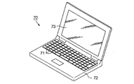
図7は、モバイル型パーソナルコンピュータの構成を示す斜視図を示す。図7において、パーソナルコンピュータ70は、キーボード71を備えた本体部72と、有機ELディスプレイ10を用いた表示ユニット73とを備えている。
この場合においても、有機ELディスプレイ10を用いた表示ユニット73は実施形態と同様な効果を発揮する。この結果、有機EL素子21の輝度階調を精度良く制御することができるとともに歩留まりや開口率を向上させることができる有機ELディスプレイ10を備えたモバイル型パーソナルコンピュータ70を提供することができる。
【0071】
図8は、携帯電話の構成を示す斜視図を示す。図8において、携帯電話80は、複数の操作ボタン81、受話口82、送話口83、有機ELディスプレイ10を用いた表示ユニット84を備えている。この場合においても、有機ELディスプレイ10を用いた表示ユニット84は上述の実施形態と同様な効果を発揮する。この結果、有機EL素子21の輝度階調を精度良く制御することができるとともに歩留まりや開口率を向上させることができる有機ELディスプレイ10を備えた携帯電話80を提供することができる。
【0072】
尚、発明の実施形態は、上記実施形態に限定されるものではなく、以下のように実施してもよい。
上述の実施形態では、画素回路20,30の駆動トランジスタQ1の導電型をp型(pチャネル)、トランジスタQ2及びスイッチングトランジスタQ3のそれぞれの導電型をn型(nチャネル)になるように設定した。そして、駆動トランジスタQ1のドレインを有機EL素子21の陽極に接続した。又、有機EL素子21の陰極を接地した。
【0073】
これを、駆動トランジスタQ1の導電型をn型(nチャネル)、スイッチングトランジスタQ3及びトランジスタQ2のそれぞれの導電型をp型(pチャネル)になるように設定してもよい。
上述の実施形態では、陽極を画素電極、陰極を複数の画素電極に対して共通の共通電極としたが、陰極を画素電極、共通電極を陽極としてもよい。
【0074】
上述の第1実施形態及び第2実施形態では、画素回路に含まれるスイッチングトランジスタQ3のゲートを第1の副走査線Yn1に接続した。又、トランジスタQ2のゲートを第2の副走査線Yn2に接続した。そして、第1の副走査線Yn1と第2の副走査線Yn2とで走査線Ynを構成した。
これに対して、図9や図10に示すように、トランジスタQ2及びスイッチングトランジスタQ3を共通の走査信号SC1で制御することもできる。
これにより、一つの画素回路に対して設けられる走査線の数は1本となり、一つの画素回路当たりの配線数を減ずることができ、開口率を向上させることができる。
【0075】
上記の実施形態では、駆動電圧Vddの画素回路に対する供給を制御する制御回路として、駆動電圧供給用トランジスタQvを使用した。
これを、駆動電圧供給用トランジスタQvの変わりに低電位と高電位との間で切換え可能なスイッチを設けてもよい。又、前記制御回路として駆動能力を向上させるためにバッファ回路あるいはソースフォロワ回路を含むボルテージフォロワ回路を使用してもよい。このようにすることによって、画素回路に対して速やかに駆動電圧Vddを供給することができる。
【0076】
上記の実施形態では、電圧供給線Loをアクティブマトリクス部12の右端側に設けたが、これに限定されることはなく、例えば、アクティブマトリクス部12の左端側に設けてもよい。
電圧供給線Loをアクティブマトリクス部12に対して走査線駆動回路13と同じ側に設けてもよい。
電源線制御回路15を、アクティブマトリクス部12に対して走査線駆動回路13と同じ側に設けることもできる。
【0077】
上記の実施形態では、本発明を有機EL素子に適用した例について述べたが、もちろん、有機EL素子以外の例えばLED、FED、液晶素子、無機EL素子、電気泳動素子、電子放出素子等の種々の電気光学素子を駆動する単位回路に具体化してもよい。RAM等(特にMRAM)の記憶素子に具体化してもよい。
【図面の簡単な説明】
【図1】第1実施形態の有機ELディスプレイの回路構成を示すブロック回路図である。
【図2】第1実施形態の表示パネル部及びデータ線駆動回路の回路構成を示すブロック回路図である。
【図3】第1実施形態の画素回路の回路図である。
【図4】第1実施形態の画素回路の駆動方法を説明するためのタイミングチャートである。
【図5】第2実施形態の表示パネル部及びデータ線駆動回路の回路構成を示すブロック回路図である。
【図6】第2実施形態の画素回路の回路図である。
【図7】第3実施形態を説明するためのモバイル型パーソナルコンピュータの構成を示す斜視図である。
【図8】第3実施形態を説明するための携帯電話の構成を示す斜視図である。
【図9】別例の画素回路を説明するための回路図である。
【図10】別例の画素回路を説明するための回路図である。
【符号の説明】
Co 容量素子としての保持用キャパシタ
Q1 第1のトランジスタとしての駆動トランジスタ
Q2 第2のトランジスタとしてのトランジスタ
Q3 第3のトランジスタとしてのスイッチングトランジスタ
Qv 制御回路又は第4のトランジスタとしての駆動電圧供給用トランジスタ
Vdd 駆動電圧
VL1 第1の電源線
VL2 第2の電源線
Xm データ線
Yn 走査線
10 電気光学装置としての有機ELディスプレイ
20,30 単位回路としての画素回路
21 電子素子、電気光学素子又は電流駆動素子としての有機EL素子
70 電子機器としてのパーソナルコンピュータ
80 電子機器としての携帯電話[0001]
TECHNICAL FIELD OF THE INVENTION
The present invention relates to an electronic circuit, a method for driving an electronic circuit, an electro-optical device, a method for driving an electro-optical device, and an electronic apparatus.
[0002]
[Prior art]
In recent years, an electro-optical device including a plurality of electro-optical elements widely used as a display device is required to have high definition or a large screen, and in response to this, each of the plurality of electro-optical elements is driven. Of the active matrix drive type electro-optical device provided with the pixel circuit for the passive drive type electro-optical device is increasing. However, in order to achieve higher definition or a larger screen, it is necessary to precisely control each of the electro-optical elements. For that purpose, it is necessary to compensate for the characteristic variation of the active elements constituting the pixel circuit.
[0003]
As a method of compensating for variations in characteristics of active elements, for example, a display device including a pixel circuit including a diode-connected transistor for compensating for variations in characteristics has been proposed (for example, see Patent Document 1).
[0004]
[Patent Document 1] JP-A-11-272233
[Problems to be solved by the invention]
By the way, a pixel circuit for compensating for variations in characteristics of active elements is generally constituted by four or more transistors, which leads to a reduction in yield and aperture ratio.
[0006]
One object of the present invention is to solve the above problems, and it is possible to reduce the number of transistors constituting a pixel circuit or a unit circuit, an electronic circuit, a driving method of an electronic circuit, an electro-optical device, An object of the present invention is to provide a driving method of an electro-optical device and an electronic apparatus.
[0007]
[Means for Solving the Problems]
The first electronic circuit of the present invention is an electronic circuit including a plurality of unit circuits, includes a first power supply line, and each of the plurality of unit circuits is connected in series to an electronic element, and A first transistor connected to one power supply line, a second transistor for controlling conduction between a drain of the first transistor and a gate of the first transistor, and a conduction state of the first transistor. A current source that outputs a data current for setting, and a third transistor that controls conduction between the first transistor and at least a part of a period during which the third transistor is in an on state Wherein the first power supply line is electrically disconnected from a driving voltage, and the first power supply line is electrically disconnected from the first power supply line during at least a part of a period in which the third transistor is off. Between the serial electronic device, wherein the current corresponding to the conductive state of the first transistor which is set by the data current to the first transistor.
In the above electronic circuit, “controlling conduction between the drain of the first transistor and the gate of the first transistor” means that the drain of the first transistor and the gate of the first transistor are connected to each other. Is not only directly connected electrically, but also includes a case where the third transistor and the like are electrically connected via an element such as another transistor or a wiring.
[0008]
A second electronic circuit according to the present invention is an electronic circuit including a plurality of unit circuits, wherein a first power supply line and a potential of the first power supply line are set to a plurality of potentials, or And a control circuit that controls supply and cutoff of a drive voltage to a power supply line, wherein each of the plurality of unit circuits is connected in series to the electronic element and the first power supply line. A first transistor connected to the first transistor, a second transistor for controlling conduction between a drain of the first transistor and a gate of the first transistor, and setting a conduction state of the first transistor. And a third transistor for controlling conduction between the first transistor and the first transistor, wherein at least a part of the period in which the third transistor is in the off state is the same as the previous one. Between the first power supply line and the electronic device, wherein the current corresponding to the conductive state of the first transistor which is set by the data current to the first transistor.
[0009]
In the above electronic circuit, the “drain” is a relative relationship between the potentials of two terminals sandwiching a channel of the first transistor when a data current flows through the first transistor and a conductivity type of the first transistor. Is determined by For example, when the first transistor is a p-type, a terminal having a lower potential among the two terminals of the first transistor is referred to as a “drain”, and when the first transistor is an n-type, A terminal having a higher potential among the two terminals of the first transistor is referred to as a “drain”.
In the above electronic circuit, the “electronic element” is, for example, an electro-optical element, a resistance element, a diode, or the like.
[0010]
A third electronic circuit according to the present invention is an electronic circuit including a plurality of unit circuits, each of the plurality of unit circuits having a first terminal, a second terminal, and a first control terminal. A first transistor, a third terminal, and a fourth terminal, wherein the third terminal is connected to the first control terminal, and an electric connection between the second terminal and the third terminal; A third transistor having a second transistor for controlling electrical connection, a fifth terminal and a sixth terminal, the third terminal having the fifth terminal connected to the first terminal, and a seventh terminal And an eighth terminal, wherein the seventh terminal includes a capacitor connected to the first control terminal and the third terminal, and wherein the first terminal includes the plurality of units. Connected to a first power supply line together with the first terminal of another unit circuit of the circuit, and the potential of the first power supply line is changed to a plurality of potentials. Set, or includes a control circuit for controlling the supply and cutoff of the drive voltage to the first power supply line.
[0011]
The first transistor, the first terminal, the second terminal, and the first control terminal are, for example, a driving transistor Q1, a source of the driving transistor Q1, It corresponds to the drain of the driving transistor Q1 and the gate of the driving transistor Q1.
[0012]
The second transistor, the third terminal, the fourth terminal, and the second control terminal correspond to the transistor Q2, the source of the transistor Q2, the drain of the transistor Q2, and the gate of the transistor Q2, respectively.
Further, the third transistor, the fifth terminal, the sixth terminal, and the third control terminal correspond to the switching transistor Q3, the source of the switching transistor Q3, the drain of the switching transistor Q3, and the gate of the switching transistor Q3, respectively. are doing.
The capacitive element, the seventh terminal, and the eighth terminal correspond to the holding capacitor Co, the first electrode La of the holding capacitor Co, and the second electrode Lb of the holding capacitor Co, respectively.
According to this, it is possible to configure a unit circuit in which the number of transistors used is reduced as compared with the conventional one.
[0013]
A fourth electronic circuit according to the present invention is an electronic circuit including a plurality of unit circuits, each of the plurality of unit circuits having a first terminal, a second terminal, and a first control terminal. A first transistor, a third terminal, and a fourth terminal, wherein the third terminal is connected to the first control terminal, and an electric connection between the second terminal and the fourth terminal; A third transistor having a second transistor for controlling electrical connection, a fifth terminal and a sixth terminal, the third terminal having the fifth terminal connected to the first terminal, and a seventh terminal And an eighth terminal, wherein the seventh terminal includes a capacitor connected to the first control terminal and the third terminal, and wherein the first terminal includes the plurality of units. A first power supply line connected to the first terminal of another unit circuit of the circuit, and the eighth terminal is connected to the plurality of unit circuits. Connected to a second power supply line held at a predetermined potential together with the eighth terminal of another unit circuit, to set the potential of the first power supply line to a plurality of potentials, or And a control circuit for controlling supply and cutoff of the drive voltage to the power supply.
According to this, a unit circuit can be configured by reducing the number of transistors to be used as compared with the conventional one, and further, the voltage can be stably held in the capacitor.
[0014]
In the above electronic circuit, the transistors included in each of the unit circuits are only the first transistor, the second transistor, and the third transistor.
According to this, the number of transistors to be used can be reduced by one as compared with the conventional one to form a unit circuit.
In the above electronic circuit, an electronic element is connected to the second terminal.
According to this, the electronic element can be controlled by a circuit using one less transistor than the conventional one.
In the above electronic circuit, the electronic element may be a current driving element.
According to this, the current driving element can be controlled by a circuit using one less transistor than the conventional one.
In the above electronic circuit, the control circuit is a fourth transistor including a ninth terminal and a tenth terminal, the ninth terminal is connected to the drive voltage, and the tenth terminal is It may be connected to the first power supply line.
According to this, the control circuit can be easily configured.
[0015]
A first method for driving an electronic circuit according to the present invention is a method for driving an electronic circuit including a plurality of unit circuits, wherein the electronic circuit includes a first power supply line, and each of the plurality of unit circuits includes: A first transistor connected in series to the electronic element and connected to the first power supply line; and a second transistor for controlling conduction between a drain of the first transistor and a gate of the first transistor. A transistor, a current source that outputs a data current for setting a conduction state of the first transistor, and a third transistor that controls conduction between the first transistor and the third transistor. A first step of supplying the data current to the first transistor as an on state, setting a conduction state of the first transistor, and turning off the third transistor; Flowing a current between the first power supply line and the electronic element in accordance with the conduction state of the first transistor, wherein the data current of the first step is transmitted to the first element. The first power supply line is electrically disconnected from a driving voltage during at least a part of a period of supplying to the one transistor, and the at least one part of a period during which the second step is performed is performed during the second step. The driving voltage is applied to one of the drain and the source of the one transistor via the first power supply line.
[0016]
A second method for driving an electronic circuit according to the present invention includes a first transistor having a first terminal, a second terminal, and a first control terminal, and a third terminal and a fourth terminal. A second transistor having the third terminal connected to the first control terminal and the fourth terminal connected to the second terminal; a fifth transistor and a sixth terminal; And a third transistor having the first terminal connected to the fifth terminal, a seventh terminal and an eighth terminal, wherein the seventh terminal is connected to the first control terminal. A plurality of unit circuits each including a terminal and a capacitor connected to the third terminal, wherein the first terminal is a first unit together with the first terminal of a series of unit circuits of the plurality of unit circuits. A method for driving an electronic circuit connected to a power supply line, wherein the first power supply line is electrically disconnected from a drive voltage. By electrically disconnecting the first terminal of the series of unit circuits from the drive voltage and turning on the third transistor of the series of unit circuits, the first transistor An amount of charge corresponding to a current level of a current flowing through the capacitor is held in the capacitive element, a voltage corresponding to the amount of charge is applied to the first control terminal, and the first terminal and the second terminal are connected to each other. Setting a conduction state between the first terminal of the series of unit circuits and electrically connecting the first terminal of the series of unit circuits to the drive voltage. ,including.
[0017]
A method for driving a third electronic circuit according to the present invention includes a first transistor having a first terminal, a second terminal, and a first control terminal, and a third terminal and a fourth terminal. A second transistor having the third terminal connected to the first control terminal and the fourth terminal connected to the second terminal, a fifth terminal and a sixth terminal, A third transistor having the first terminal connected to the fifth terminal, a seventh terminal and an eighth terminal, wherein the seventh terminal is the first control terminal. And a plurality of unit circuits each including a capacitor connected to the third terminal, wherein the first terminal is a first unit together with the first terminal of a series of unit circuits of the plurality of unit circuits. The eighth terminal is connected to a power supply line, and the eighth terminal is an eighth terminal of a series of unit circuits of the plurality of unit circuits. A method for driving an electronic circuit both connected to a second power supply line, wherein the first terminal of the series of unit circuits is electrically disconnected from the drive voltage by electrically disconnecting the first power supply line from a drive voltage. By electrically disconnecting from the driving voltage, and by turning on the third transistor of the series of unit circuits, the amount of charge according to the current level of the current flowing through the first transistor is reduced. Holding a capacitor, applying a voltage corresponding to the amount of charge to the first control terminal, and setting a conduction state between the first terminal and the second terminal; Turning off a third transistor and electrically connecting the first terminal of the series of unit circuits to the drive voltage.
According to the above electronic circuit driving method, the number of transistors in the unit circuit can be reduced as much as possible.
[0018]
A first electro-optical device of the present invention includes a plurality of scanning lines, a plurality of data lines, a plurality of first power lines, and a plurality of unit circuits, each of the plurality of unit circuits being: A first transistor connected in series to the electro-optical element and connected to a corresponding first power supply line among the first power supply lines; and a drain of the first transistor and the first transistor. A second transistor for controlling conduction with a gate, and controlling conduction between the first transistor and a corresponding data line among the plurality of data lines, via a corresponding one of the plurality of scanning lines. A third transistor controlled by a scan signal supplied to the first power supply line during a period in which at least a part of the third transistor is on. From While the data transistor supplied from the corresponding data line flows through the first transistor to set the conduction state of the first transistor and the third transistor to be in the off state In at least a part of the period, the drive voltage is applied to one of the drain and the source of the first transistor, and between the corresponding first power supply line and the electro-optical element, A current according to the conduction state of the first transistor set by the data current flows.
[0019]
In the above electro-optical device, “controlling conduction between the drain of the first transistor and the gate of the first transistor” means “the drain of the first transistor and the gate of the first transistor”. Is directly connected electrically, and also includes a case where the third transistor and the like are electrically connected via an element such as another transistor or the corresponding data line or the like.
[0020]
A second electro-optical device according to the present invention is an electro-optical device including a plurality of scanning lines, a plurality of data lines, and a plurality of unit circuits, wherein each of the plurality of unit circuits is a first unit. A first transistor having a first terminal, a second terminal, and a first control terminal; and a third transistor having a third terminal, a fourth terminal, and a second control terminal. A second transistor having a terminal connected to the third terminal, a fifth terminal, a sixth terminal, and a third control terminal, wherein the fifth terminal is connected to the first terminal; A third terminal in which the sixth terminal is connected to one of the plurality of data lines, and the third control terminal is connected to one of the plurality of scan lines. , A seventh terminal and an eighth terminal, wherein the seventh terminal is the first control terminal and the third terminal Connected to a first power supply line together with the first terminals of the other unit circuits of the plurality of unit circuits, and a potential of the first power supply line. Is set to a plurality of potentials, or a control circuit is provided for controlling the supply and cutoff of the drive voltage to the power supply line.
[0021]
A third electro-optical device according to the present invention is an electro-optical device including a plurality of scanning lines, a plurality of data lines, and a plurality of unit circuits, wherein each of the plurality of unit circuits is a first unit. A first transistor having a first terminal, a second terminal, and a first control terminal; and a third transistor having a third terminal, a fourth terminal, and a second control terminal. A third transistor connected to the terminal, a second transistor controlling an electrical connection between the second terminal and the fourth terminal, a fifth terminal, a sixth terminal, and a third control terminal; A fifth terminal connected to the first terminal, a sixth terminal connected to one of the plurality of data lines, and a third control terminal. Has a third transistor connected to one of the plurality of scanning lines, a seventh terminal and an eighth terminal, A seventh terminal includes a capacitor connected to the first control terminal and the third terminal, and the first terminal is connected to the first unit of the other unit circuits of the plurality of unit circuits. A second power supply line connected to a first power supply line held at a predetermined potential together with the eighth terminal of another unit circuit of the plurality of unit circuits; A control circuit is provided for setting the potential of the first power supply line to a plurality of potentials, or controlling supply and cutoff of a drive voltage to the first power supply line.
In the above electro-optical device, the number of transistors in the unit circuit can be reduced as much as possible.
[0022]
In the electro-optical device described above, it is preferable that the transistors included in each of the unit circuits are only the first transistor, the second transistor, and the third transistor.
[0023]
In the above electro-optical device, the control circuit is a fourth transistor including a ninth terminal and a tenth terminal, the ninth terminal is connected to the drive voltage, and the tenth terminal is Preferably, it is connected to the first power supply line.
[0024]
According to this, the control circuit can be easily configured.
In the above electro-optical device, the electro-optical element may be, for example, an EL element. Among them, a current driving element such as an organic EL element is preferable.
[0025]
A first method for driving an electro-optical device according to the present invention is a method for driving an electro-optical device, wherein the electro-optical device includes a plurality of scanning lines, a plurality of data lines, and a plurality of first power lines. , A plurality of unit circuits, each of the plurality of unit circuits being connected in series to an electro-optical element and being connected to a corresponding first power supply line among the first power supply lines. , A second transistor for controlling conduction between the drain of the first transistor and a gate of the first transistor, and a corresponding data line among the first transistor and the plurality of data lines A third transistor controlled by a scanning signal supplied through a corresponding scanning line among the plurality of scanning lines, wherein the third transistor is turned on and the corresponding First A first transistor for setting a conduction state of the first transistor by flowing a data current supplied from the corresponding data line to the first transistor in a state where the power supply line is electrically disconnected from the drive voltage; And in a state where the third transistor is off and the drive voltage is applied to one of the drain and source of the first transistor via the corresponding first power supply line, A second step of flowing a current between the corresponding first power supply line and the electro-optical element according to the conduction state of the first transistor set by the data current. And
[0026]
According to a second method for driving an electro-optical device of the present invention, a first transistor having a first terminal, a second terminal, and a first control terminal; a third terminal; a fourth terminal; A second transistor having a second control terminal, a third terminal connected to the first control terminal, and a fourth terminal connected to the second terminal; A third transistor having a first terminal, a sixth terminal, and a third control terminal, wherein the first terminal is connected to the fifth terminal, a seventh terminal and an eighth terminal. A plurality of unit circuits, each of which includes a capacitive element whose seventh terminal is connected to the first control terminal and the third terminal, and an electro-optical element connected to the second terminal. , The sixth terminal is connected to one of the plurality of data lines, and the third control terminal is connected to one of the plurality of scanning lines. A driving method for an electro-optical device, wherein the first terminal is connected to a first power supply line together with the first terminals of the other unit circuits of the plurality of unit circuits, By electrically disconnecting the first power supply line from the driving voltage, the first terminal of the series of unit circuits is electrically disconnected from the driving voltage, and the third terminal of the series of unit circuits is electrically disconnected. Is turned on, the amount of charge corresponding to the current level of the current flowing through the first transistor is held in the capacitive element, and the voltage corresponding to the amount of charge is controlled by the first control. Setting a conduction state between the first terminal and the second terminal by applying a voltage to the first terminal and turning off the third transistor; 1 terminal is connected to the first terminal. Through the power line and a step of electrically connecting to the driving voltage.
[0027]
According to a third method for driving an electro-optical device of the present invention, a first transistor having a first terminal, a second terminal, and a first control terminal; a third terminal; a fourth terminal; A second transistor having a second control terminal, a third terminal connected to the first control terminal, and a fourth terminal connected to the second terminal; A third transistor having a first terminal, a sixth terminal, and a third control terminal, wherein the first terminal is connected to the fifth terminal, a seventh terminal and an eighth terminal. A plurality of unit circuits, each including a capacitor whose seventh terminal is connected to the first control terminal and the third terminal, and an electro-optical element connected to the second terminal. Wherein the sixth terminal is connected to one of a plurality of data lines, and the third control terminal is connected to a plurality of scanning lines. One scanning line, the first terminal is connected to a first power supply line together with the first terminal of another unit circuit of the plurality of unit circuits, and the eighth terminal is connected to the plurality of unit circuits. A driving method of an electro-optical device connected to a second power supply line together with the eighth terminal of another unit circuit of the unit circuit, wherein the first power supply line is electrically disconnected from a driving voltage. By electrically disconnecting the first terminal of the series of unit circuits from the drive voltage and turning on the third transistor of the series of unit circuits, The amount of charge corresponding to the current level of the flowing current is held in the capacitor, and a voltage corresponding to the amount of charge is applied to the first control terminal, so that the first terminal and the second terminal Set the conduction state with the terminal And step, as well as to the third transistor in the OFF state of, and a step of electrically connecting said first terminal of said series of unit circuits to the driving voltage through the first power line.
[0028]
According to the above-described method of driving an electro-optical device, it is possible to compensate for variations in characteristics of a transistor that determines a current or a voltage to be supplied to an electro-optical element, and to reduce the number of transistors included in a pixel circuit as much as possible.
[0029]
A first electronic device according to the present invention is characterized by mounting the above electronic circuit.
The above electronic circuit can be used for an active drive unit having an active function, such as a display unit or a memory unit of the electronic device.
[0030]
According to a second aspect of the invention, there is provided a second electronic apparatus including the above-described electro-optical device.
Since the above-described electro-optical device can control the state of the electro-optical element with high precision and has a high aperture ratio, it is possible to provide an electronic apparatus having a display unit with excellent display quality.
Further, in the above-described electro-optical device, the number of transistors constituting the pixel circuit is reduced as much as possible, so that the manufacturing cost can be suppressed.
[0031]
BEST MODE FOR CARRYING OUT THE INVENTION
(1st Embodiment)
Hereinafter, a first embodiment of the present invention will be described with reference to FIGS. FIG. 1 is a block circuit diagram showing a circuit configuration of an organic EL display as an electro-optical device. FIG. 2 is a block circuit diagram showing a circuit configuration of the display panel unit and the data line driving circuit. FIG. 3 is a circuit diagram of the pixel circuit. FIG. 4 is a timing chart for explaining a driving method of the pixel circuit.
[0032]
The
[0033]
The
[0034]
As shown in FIG. 2, the
[0035]
That is, the
[0036]
As shown in FIG. 2, the
[0037]
The scanning
[0038]
The data line driving
[0039]
The power supply
Then, when the drive voltage supply transistor Qv is turned on, the drive voltage Vdd is supplied to the first power supply line VL1, and the drive voltage Vdd is supplied to the
[0040]
Next, the
As shown in FIG. 3, the
[0041]
The conductivity type of drive transistor Q1 is p-type (p-channel). The conductivity types of the transistor Q2 and the switching transistor Q3 are n-type (n-channel).
[0042]
The drive transistor Q1 has its drain connected to the anode of the
[0043]
The gate of the driving transistor Q1 is connected to the first electrode La of the holding capacitor Co, and the second electrode Lb of the holding capacitor Co is connected to the source of the driving transistor Q1.
[0044]
The source of the driving transistor Q1 is connected to the source of the switching transistor Q3. The drain of the switching transistor Q3 is connected to the data line Xm. The gate of the switching transistor Q3 is connected to the first sub-scanning line Yn1. Note that the first sub-scanning line Yn1 and the second sub-scanning line Yn2 constitute a scanning line Yn.
[0045]
The source of the driving transistor Q1 is connected to the first power supply line VL1 together with the source of the driving transistor Q1 of another
[0046]
The conductivity type of the driving voltage supply transistor Qv is p-type (p-channel). The drive voltage supply transistor Qv responds to a power supply line control signal SFC supplied from the power supply
[0047]
Next, a driving method of the
[0048]
First, as shown in FIG. 4, a data current Idata is supplied from the data
[0049]
As a result, the switching transistor Q3 and the transistor Q2 are turned on. Then, the data current Idata flows via the driving transistor Q1. As a result, the charge amount corresponding to the data current Idata is held in the holding capacitor Co, and the conduction state between the source and the drain of the drive transistor Q1 is set according to the gate voltage Vo corresponding to the charge amount.
[0050]
Thereafter, a first scanning signal SC1 for turning off the switching transistor Q3 is supplied from the scanning
[0051]
As a result, the switching transistor Q3 and the transistor Q2 are turned off, and the data line Xm and the driving transistor Q1 are electrically disconnected.
Note that at least during the period when the data current Idata is being supplied to the drive transistor Q1, the drive voltage supply transistor Qv turns off the drive voltage supply transistor Qv supplied from the power supply
[0052]
Subsequently, a power supply line control signal Sv for turning on the drive voltage supply transistor Qv is supplied from the power supply
[0053]
Thereby, the drive current Iel according to the conduction state set by the data current is supplied to the
By using the data current Idata as the data signal as described above, variations in various parameters of the electrical characteristics of the driving transistor Q1, such as the threshold voltage and the gain coefficient, can be compensated for each driving transistor Q1.
Until the driving voltage supply transistor Qv is turned off, the
As described above, the
[0054]
According to the electronic circuit and the electro-optical device of the above embodiment, the following features can be obtained.
[0055]
(1) In the present embodiment, the
[0056]
With this configuration, the number of transistors used in the
[0057]
(2nd Embodiment)
Next, a second embodiment of the present invention will be described with reference to FIG. In the present embodiment, the same components as those in the above-described first embodiment have the same reference numerals, and a detailed description thereof will be omitted.
[0058]
FIG. 5 is a block circuit diagram illustrating a circuit configuration of the active matrix unit 12a and the data line driving
[0059]
In the
[0060]
As shown in FIG. 6, the
[0061]
The drive transistor Q1 has its drain connected to the anode of the
[0062]
The second electrode Lb of the holding capacitor Co is connected to the second power supply line VL2. As a result, the drive voltage Vdd, which is a constant voltage, is constantly and independently supplied to the holding capacitor Co independently of the on / off state of the drive voltage supply transistor Qv.
By connecting the second electrode Lb of the holding capacitor Co to the second power supply line VL2 in this manner, when the data current Idata is supplied to the drive transistor Q1, and when a drive voltage is applied to the source of the drive transistor Q1. At times, it is possible to suppress the fluctuation of the voltage generated in the holding capacitor Co.
As a result, the
[0063]
The source of the driving transistor Q1 is connected to the first power supply line VL and to the source of the switching transistor Q3. The drain of the switching transistor Q3 is connected to the data line Xm. The gate of the switching transistor Q3 is connected to the first sub-scanning line Yn1.
[0064]
Next, a method of driving the
First, the data current Idata is supplied from the data
[0065]
Then, the switching transistor Q3 and the transistor Q2 are turned on. Then, the data current Idata passes through the driving transistor Q1 and the transistor Q2, and the charge corresponding to the data current Idata is held in the holding capacitor Co.
[0066]
As a result, the conduction state between the source and the drain of the driving transistor Q1 is set.
[0067]
Thereafter, a first scanning signal SC1 for turning off the switching transistor Q3 is supplied from the scanning
Note that at least during the period when the data current Idata is being supplied to the drive transistor Q1, the drive voltage supply transistor Qv turns off the drive voltage supply transistor Qv supplied from the power supply
[0068]
Subsequently, a power supply line control signal Sv for turning on the drive voltage supply transistor Qv is supplied from the power supply
[0069]
(Third embodiment)
Next, application of the electronic apparatus of the
[0070]
FIG. 7 is a perspective view showing the configuration of a mobile personal computer. 7, a
Also in this case, the
[0071]
FIG. 8 is a perspective view illustrating a configuration of a mobile phone. In FIG. 8, a
[0072]
The embodiments of the present invention are not limited to the above embodiments, but may be implemented as follows.
In the above-described embodiment, the conductivity type of the drive transistor Q1 of the
[0073]
This may be set so that the conductivity type of the driving transistor Q1 is n-type (n-channel) and the conductivity types of the switching transistor Q3 and the transistor Q2 are p-type (p-channel).
In the above embodiment, the anode is a pixel electrode and the cathode is a common electrode common to a plurality of pixel electrodes. However, the cathode may be a pixel electrode and the common electrode may be an anode.
[0074]
In the above-described first and second embodiments, the gate of the switching transistor Q3 included in the pixel circuit is connected to the first sub-scanning line Yn1. Further, the gate of the transistor Q2 was connected to the second sub-scanning line Yn2. The first sub-scanning line Yn1 and the second sub-scanning line Yn2 constituted the scanning line Yn.
On the other hand, as shown in FIGS. 9 and 10, the transistor Q2 and the switching transistor Q3 can be controlled by the common scanning signal SC1.
Thus, the number of scanning lines provided for one pixel circuit is one, the number of wirings per pixel circuit can be reduced, and the aperture ratio can be improved.
[0075]
In the above embodiment, the drive voltage supply transistor Qv is used as a control circuit for controlling the supply of the drive voltage Vdd to the pixel circuit.
A switch capable of switching between a low potential and a high potential may be provided instead of the drive voltage supply transistor Qv. Further, a voltage follower circuit including a buffer circuit or a source follower circuit may be used as the control circuit in order to improve the driving capability. By doing so, the drive voltage Vdd can be quickly supplied to the pixel circuit.
[0076]
In the above embodiment, the voltage supply line Lo is provided on the right end side of the
The voltage supply line Lo may be provided on the same side as the scanning
The power supply
[0077]
In the above-described embodiment, an example in which the present invention is applied to an organic EL element has been described. May be embodied as a unit circuit for driving the electro-optical element. The present invention may be embodied in a storage element such as a RAM (in particular, an MRAM).
[Brief description of the drawings]
FIG. 1 is a block circuit diagram illustrating a circuit configuration of an organic EL display according to a first embodiment.
FIG. 2 is a block circuit diagram illustrating a circuit configuration of a display panel unit and a data line driving circuit according to the first embodiment.
FIG. 3 is a circuit diagram of a pixel circuit according to the first embodiment.
FIG. 4 is a timing chart for explaining a driving method of the pixel circuit according to the first embodiment.
FIG. 5 is a block circuit diagram illustrating a circuit configuration of a display panel unit and a data line driving circuit according to a second embodiment.
FIG. 6 is a circuit diagram of a pixel circuit according to a second embodiment.
FIG. 7 is a perspective view showing a configuration of a mobile personal computer for explaining a third embodiment.
FIG. 8 is a perspective view showing a configuration of a mobile phone for explaining a third embodiment.
FIG. 9 is a circuit diagram for explaining another example of a pixel circuit.
FIG. 10 is a circuit diagram illustrating another example of a pixel circuit.
[Explanation of symbols]
Co Holding capacitor Q1 as capacitance element Driving transistor Q2 as first transistor Transistor Q3 as second transistor Switching transistor Qv as third transistor Control circuit or driving voltage supply transistor Vdd as fourth transistor Drive voltage VL1 First power supply line VL2 Second power supply line Xm Data line
Claims (23)
第1の電源線を含み、
前記複数の単位回路の各々は、電子素子に直列に接続されるともに前記第1の電源線に接続された第1のトランジスタと、
前記第1のトランジスタのドレインと前記第1のトランジスタのゲートとの導通を制御する第2のトランジスタと、
前記第1のトランジスタの導通状態を設定するためのデータ電流を出力する電流源と前記第1のトランジスタとの導通を制御する第3のトランジスタと、を備え、
前記第3のトランジスタがオン状態にある期間のうち少なくとも1部の期間において、前記第1の電源線は駆動電圧から電気的に切断され、
前記第3のトランジスタがオフ状態にある期間のうち少なくとも1部の期間において、前記第1の電源線と前記電子素子との間に、前記第1のトランジスタに前記データ電流により設定された前記第1のトランジスタの導通状態に応じた電流が流れることを特徴とする電子回路。An electronic circuit including a plurality of unit circuits,
Including a first power line,
Each of the plurality of unit circuits is connected in series to an electronic element and connected to the first power supply line;
A second transistor for controlling conduction between a drain of the first transistor and a gate of the first transistor;
A current source that outputs a data current for setting a conduction state of the first transistor, and a third transistor that controls conduction between the first transistor and
The first power supply line is electrically disconnected from a driving voltage during at least a part of a period in which the third transistor is in an on state,
In at least a part of a period in which the third transistor is in an off state, the third transistor set between the first power supply line and the electronic element by the data current in the first transistor is provided. An electronic circuit, wherein a current flows according to a conduction state of one transistor.
第1の電源線と、
前記第1の電源線の電位を制御する制御回路と、を含み、
前記複数の単位回路の各々は、電子素子に直列に接続されるともに前記第1の電源線に接続された第1のトランジスタと、
前記第1のトランジスタのドレインと前記第1のトランジスタとのゲートとの導通を制御する第2のトランジスタと、
前記第1のトランジスタの導通状態を設定するためのデータ電流を出力する電流源と前記第1のトランジスタとの導通を制御する第3のトランジスタと、を備え、
前記第3のトランジスタがオフ状態にある期間のうち少なくとも1部の期間において、前記第1の電源線と前記電子素子との間に、前記第1のトランジスタに前記データ電流により設定された前記第1のトランジスタの導通状態に応じた電流が流れることを特徴とする電子回路。An electronic circuit including a plurality of unit circuits,
A first power line;
A control circuit for controlling the potential of the first power supply line,
Each of the plurality of unit circuits is connected in series to an electronic element and connected to the first power supply line;
A second transistor for controlling conduction between a drain of the first transistor and a gate of the first transistor;
A current source that outputs a data current for setting a conduction state of the first transistor, and a third transistor that controls conduction between the first transistor and
In at least a part of a period in which the third transistor is in an off state, the third transistor set between the first power supply line and the electronic element by the data current in the first transistor is provided. An electronic circuit, wherein a current flows according to a conduction state of one transistor.
前記複数の単位回路の各々は、
第1の端子と第2の端子と第1の制御用端子とを有する第1のトランジスタと、
第3の端子と第4の端子とを有し、前記第1の制御用端子に前記第3の端子が接続され、前記2の端子と前記第3の端子との電気的接続を制御する第2のトランジスタと、
第5の端子と第6の端子とを有し、前記第1の端子に前記第5の端子が接続された第3のトランジスタと、を含み、
前記第1の端子は前記複数の単位回路の他の単位回路の前記第1の端子と共に第1の電源線に接続され、
前記第1の電源線の電位を複数の電位に設定する、あるいは、前記第1の電源線への駆動電圧の供給及び遮断を制御する制御回路を備えていることを特徴とする電子回路。An electronic circuit including a plurality of unit circuits,
Each of the plurality of unit circuits,
A first transistor having a first terminal, a second terminal, and a first control terminal;
A third terminal having a third terminal and a fourth terminal, wherein the third terminal is connected to the first control terminal, and controls an electrical connection between the second terminal and the third terminal; Two transistors,
A third transistor having a fifth terminal and a sixth terminal, the third transistor having the first terminal connected to the fifth terminal;
The first terminal is connected to a first power supply line together with the first terminals of other unit circuits of the plurality of unit circuits,
An electronic circuit, comprising: a control circuit that sets the potential of the first power supply line to a plurality of potentials, or controls supply and cutoff of a drive voltage to the first power supply line.
前記複数の単位回路の各々は、
第1の端子と第2の端子と第1の制御用端子とを有する第1のトランジスタと、
第3の端子と第4の端子とを有し、前記第1の制御用端子に前記第3の端子が接続され、前記2の端子と前記第3の端子との電気的接続を制御する第2のトランジスタと、
第5の端子と第6の端子とを有し、前記第1の端子に前記第5の端子が接続された第3のトランジスタと、
第7の端子と第8の端子とを有し、前記第7の端子が前記第1の制御用端子及び前記第3の端子に接続された容量素子と、を含み、
前記第1の端子は前記複数の単位回路の他の単位回路の前記第1の端子と共に第1の電源線に接続され、
前記第1の電源線の電位を複数の電位に設定する、あるいは、前記第1の電源線への駆動電圧の供給及び遮断を制御する制御回路を備えていることを特徴とする電子回路。An electronic circuit including a plurality of unit circuits,
Each of the plurality of unit circuits,
A first transistor having a first terminal, a second terminal, and a first control terminal;
A third terminal having a third terminal and a fourth terminal, wherein the third terminal is connected to the first control terminal, and controls an electrical connection between the second terminal and the third terminal; Two transistors,
A third transistor, having a fifth terminal and a sixth terminal, wherein the first terminal is connected to the fifth terminal;
A capacitor having a seventh terminal and an eighth terminal, wherein the seventh terminal includes a capacitor connected to the first control terminal and the third terminal;
The first terminal is connected to a first power supply line together with the first terminals of other unit circuits of the plurality of unit circuits,
An electronic circuit, comprising: a control circuit that sets the potential of the first power supply line to a plurality of potentials, or controls supply and cutoff of a drive voltage to the first power supply line.
前記複数の単位回路の各々は、
第1の端子と第2の端子と第1の制御用端子とを有する第1のトランジスタと、
第3の端子と第4の端子とを有し、前記第1の制御用端子に前記第3の端子が接続され、前記2の端子と前記第3の端子との電気的接続を制御する第2のトランジスタと、
第5の端子と第6の端子とを有し、前記第1の端子に前記第5の端子が接続された第3のトランジスタと、
第7の端子と第8の端子とを有し、前記第7の端子が前記第1の制御用端子及び前記第3の端子に接続された容量素子と、を含み、
前記第1の端子は前記複数の単位回路の他の単位回路の前記第1の端子と共に第1の電源線に接続され、
前記第8の端子は前記複数の単位回路の他の単位回路の前記第8の端子と共に所定電位に保持された第2の電源線に接続され、
前記第1の電源線の電位を複数の電位に設定する、あるいは、前記第1の電源線への駆動電圧の供給及び遮断を制御する制御回路を備えていることを特徴とする電子回路。An electronic circuit including a plurality of unit circuits,
Each of the plurality of unit circuits,
A first transistor having a first terminal, a second terminal, and a first control terminal;
A third terminal having a third terminal and a fourth terminal, wherein the third terminal is connected to the first control terminal, and controls an electrical connection between the second terminal and the third terminal; Two transistors,
A third transistor, having a fifth terminal and a sixth terminal, wherein the first terminal is connected to the fifth terminal;
A capacitor having a seventh terminal and an eighth terminal, wherein the seventh terminal includes a capacitor connected to the first control terminal and the third terminal;
The first terminal is connected to a first power supply line together with the first terminals of other unit circuits of the plurality of unit circuits,
The eighth terminal is connected to a second power supply line held at a predetermined potential together with the eighth terminals of the other unit circuits of the plurality of unit circuits,
An electronic circuit, comprising: a control circuit that sets the potential of the first power supply line to a plurality of potentials, or controls supply and cutoff of a drive voltage to the first power supply line.
前記単位回路の各々に含まれるトランジスタは、前記第1のトランジスタ、前記第2のトランジスタ及び前記第3のトランジスタのみであることを特徴とする電子回路。The electronic circuit according to any one of claims 1 to 5,
The electronic circuit according to claim 1, wherein the transistors included in each of the unit circuits are only the first transistor, the second transistor, and the third transistor.
前記第2の端子には電子素子が接続されていることを特徴とする電子回路。The electronic circuit according to any one of claims 3 to 6,
An electronic circuit, wherein an electronic element is connected to the second terminal.
前記電子素子が電流駆動素子であることを特徴とする電子回路。The electronic circuit according to any one of claims 1 to 7,
An electronic circuit, wherein the electronic element is a current driving element.
前記制御回路は第9の端子と第10の端子とを備えた第4のトランジスタであり、
前記第9の端子は前記駆動電圧に接続され、前記第10の端子は前記第1の電源線に接続されていることを特徴とする電子回路。The electronic circuit according to any one of claims 2 to 5,
The control circuit is a fourth transistor having a ninth terminal and a tenth terminal,
An electronic circuit, wherein the ninth terminal is connected to the drive voltage, and the tenth terminal is connected to the first power supply line.
前記電子回路は、
第1の電源線を含み、
前記複数の単位回路の各々は、電子素子に直列に接続されるともに前記第1の電源線に接続された第1のトランジスタと、
前記第1のトランジスタのドレインと前記第1のトランジスタとのゲートとの導通を制御する第2のトランジスタと、
前記第1のトランジスタの導通状態を設定するためのデータ電流を出力する電流源と前記第1のトランジスタとの導通を制御する第3のトランジスタと、を備え、
前記第3のトランジスタをオン状態として前記データ電流を前記第1のトランジスタに供給し、前記第1のトランジスタの導通状態を設定する第1のステップと、
前記第3のトランジスタをオフ状態とし、前記第1の電源線と前記電子素子との間に前記第1のトランジスタの前記導通状態に応じた電流を流す第2のステップと、を含み、
前記第1のステップの前記データ電流を前記第1のトランジスタに供給する期間の少なくとも1部の期間において、前記第1の電源線を駆動電圧から電気的に切り離し、
前記第2のステップを行っている期間の少なくとも1部の期間において、前記第1のトランジスタの前記ドレイン及びソースのいずれか一方に前記第1の電源線を介して前記駆動電圧を印加すること、
を特徴とする電子回路の駆動方法。A method for driving an electronic circuit including a plurality of unit circuits,
The electronic circuit includes:
Including a first power line,
Each of the plurality of unit circuits is connected in series to an electronic element and connected to the first power supply line;
A second transistor for controlling conduction between a drain of the first transistor and a gate of the first transistor;
A current source that outputs a data current for setting a conduction state of the first transistor, and a third transistor that controls conduction between the first transistor and
A first step of turning on the third transistor, supplying the data current to the first transistor, and setting a conductive state of the first transistor;
Turning off the third transistor, and flowing a current between the first power supply line and the electronic element according to the conduction state of the first transistor,
Electrically disconnecting the first power supply line from a driving voltage during at least a part of a period of supplying the data current to the first transistor in the first step;
Applying the driving voltage to one of the drain and the source of the first transistor via the first power supply line during at least a part of the period in which the second step is being performed;
A method for driving an electronic circuit, comprising:
第3の端子と第4の端子とを有し、前記第1の制御用端子に前記第3の端子が接続され、前記第2の端子に前記第4の端子が接続された第2のトランジスタと、
第5の端子と第6の端子とを有し、前記第1の端子に前記第5の端子が接続された第3のトランジスタと、
第7の端子及び第8の端子を有し、前記第7の端子が前記第1の制御用端子及び前記第3の端子に接続された容量素子と、を含む単位回路を複数備え、
前記第1の端子は前記複数の単位回路のうちの一連の単位回路の前記第1の端子と共に第1の電源線に接続されている電子回路の駆動方法であって、
前記第1の電源線を駆動電圧から電気的に切り離すことにより、前記一連の単位回路の前記第1の端子を前記駆動電圧から電気的に切り離し、かつ、前記一連の単位回路の前記第3のトランジスタをオン状態とすることにより、前記第1のトランジスタを経由して流れる電流の電流レベルに応じた電荷量を前記容量素子に保持し、前記電荷量に応じた電圧を前記第1の制御用端子に印加して、前記第1の端子と前記第2の端子との間の導通状態を設定するステップと、
前記第3のトランジスタをオフ状態にするとともに、前記一連の単位回路の前記第1の端子を前記駆動電圧に電気的に接続にするステップと、
を含むことを特徴とする電子回路の駆動方法。A first transistor having a first terminal, a second terminal, and a first control terminal;
A second transistor having a third terminal and a fourth terminal, the third terminal being connected to the first control terminal, and the fourth terminal being connected to the second terminal; When,
A third transistor, having a fifth terminal and a sixth terminal, wherein the first terminal is connected to the fifth terminal;
A plurality of unit circuits each including a seventh terminal and an eighth terminal, wherein the seventh terminal includes a capacitor connected to the first control terminal and the third terminal;
A method for driving an electronic circuit, wherein the first terminal is connected to a first power supply line together with the first terminal of a series of unit circuits of the plurality of unit circuits,
By electrically disconnecting the first power supply line from the driving voltage, the first terminal of the series of unit circuits is electrically disconnected from the driving voltage, and the third terminal of the series of unit circuits is electrically disconnected. By turning on the transistor, a charge amount corresponding to a current level of a current flowing through the first transistor is held in the capacitor, and a voltage corresponding to the charge amount is stored in the first control transistor. Applying a voltage to a terminal to set a conduction state between the first terminal and the second terminal;
Turning off the third transistor and electrically connecting the first terminal of the series of unit circuits to the drive voltage;
A method for driving an electronic circuit, comprising:
第3の端子と第4の端子とを有し、前記第1の制御用端子に前記第3の端子が接続され、前記第2の端子に前記第4の端子が接続された第2のトランジスタと、
第5の端子と第6の端子とを有し、前記第1の端子に前記第5の端子が接続された第3のトランジスタと、
第7の端子及び第8の端子を有し、前記第7の端子が前記第1の制御用端子及び前記第3の端子に接続された容量素子と、を含む単位回路を複数備え、
前記第1の端子は前記複数の単位回路のうちの一連の単位回路の前記第1の端子と共に第1の電源線に接続されるとともに、
前記第8の端子は前記複数の単位回路のうちの一連の単位回路の前記第8の端子と共に第2の電源線に接続されている電子回路の駆動方法であって、
前記第1の電源線を駆動電圧から電気的に切り離すことにより、前記一連の単位回路の前記第1の端子を前記駆動電圧から電気的に切り離し、かつ、前記一連の単位回路の前記第3のトランジスタがオン状態とすることにより、前記第1のトランジスタを経由して流れる電流の電流レベルに応じた電荷量を前記容量素子に保持し、前記電荷量に応じた電圧を前記第1の制御用端子に印加して、前記第1の端子と前記第2の端子との間の導通状態を設定するステップと、
前記第3のトランジスタをオフ状態にするとともに、前記一連の単位回路の前記第1の端子を前記駆動電圧に電気的に接続するステップと
を含むことを特徴とする電子回路の駆動方法。A first transistor having a first terminal, a second terminal, and a first control terminal;
A second transistor having a third terminal and a fourth terminal, the third terminal being connected to the first control terminal, and the fourth terminal being connected to the second terminal; When,
A third transistor, having a fifth terminal and a sixth terminal, wherein the first terminal is connected to the fifth terminal;
A plurality of unit circuits each including a seventh terminal and an eighth terminal, wherein the seventh terminal includes a capacitor connected to the first control terminal and the third terminal;
The first terminal is connected to a first power supply line together with the first terminals of a series of unit circuits of the plurality of unit circuits,
A method for driving an electronic circuit, wherein the eighth terminal is connected to a second power supply line together with the eighth terminal of a series of unit circuits of the plurality of unit circuits,
By electrically disconnecting the first power supply line from the driving voltage, the first terminal of the series of unit circuits is electrically disconnected from the driving voltage, and the third terminal of the series of unit circuits is electrically disconnected. When the transistor is turned on, a charge corresponding to a current level of a current flowing through the first transistor is held in the capacitor, and a voltage corresponding to the charge is used for the first control. Applying a voltage to a terminal to set a conduction state between the first terminal and the second terminal;
Turning off the third transistor and electrically connecting the first terminals of the series of unit circuits to the drive voltage.
複数のデータ線と、
複数の第1の電源線と、
複数の単位回路と、を含み、
前記複数の単位回路の各々は、
電気光学素子に直列に接続されるともに前記第1の電源線のうち対応する第1の電源線に接続された第1のトランジスタと、
前記第1のトランジスタの前記ドレインと前記第1のトランジスタとのゲートとの導通を制御する第2のトランジスタと、
前記第1のトランジスタと前記複数のデータ線のうち対応するデータ線との導通を制御し、前記複数の走査線のうち対応する走査線を介して供給される走査信号により制御される第3のトランジスタと、を備え、
前記第3のトランジスタがオン状態にある期間のうち少なくとも1部の期間において、
前記対応する第1の電源線は駆動電圧から電気的に切り離されるとともに、前記対応するデータ線から供給されるデータ電流が前記第1のトランジスタに流れることにより前記第1のトランジスタの導通状態が設定され、
前記第3のトランジスタがオフ状態にある期間のうち少なくとも1部の期間において、
前記第1のトランジスタの前記ドレイン及びソースのうちいずれか一方に前記駆動電圧が印加され、前記対応する第1の電源線と前記電気光学素子との間に、前記データ電流により設定された前記第1のトランジスタの前記導通状態に応じた電流が流れること、
を特徴とする電気光学装置。Multiple scan lines;
Multiple data lines,
A plurality of first power lines;
And a plurality of unit circuits,
Each of the plurality of unit circuits,
A first transistor connected in series to the electro-optical element and connected to a corresponding first power supply line among the first power supply lines;
A second transistor for controlling conduction between the drain of the first transistor and a gate of the first transistor;
A third transistor that controls conduction between the first transistor and a corresponding data line among the plurality of data lines, and is controlled by a scan signal supplied through a corresponding scan line among the plurality of scan lines; And a transistor,
In at least a part of the period in which the third transistor is on,
The corresponding first power supply line is electrically disconnected from the drive voltage, and the data current supplied from the corresponding data line flows through the first transistor, thereby setting the conduction state of the first transistor. And
In at least a part of the period in which the third transistor is off,
The drive voltage is applied to one of the drain and the source of the first transistor, and the first voltage set by the data current between the corresponding first power supply line and the electro-optical element. A current corresponding to the conduction state of one transistor flows;
An electro-optical device comprising:
前記複数の単位回路の各々は、
第1の端子と第2の端子と第1の制御用端子とを有する第1のトランジスタと、
第3の端子と第4の端子と第2の制御用端子とを有し、前記第1の制御用端子に前記第3の端子が接続された第2のトランジスタと、
第5の端子と第6の端子と第3の制御用端子とを有し、前記第5の端子が前記第1の端子に接続され、前記第6の端子が前記複数のデータ線のうちの一つのデータ線に接続され、前記第3の制御用端子が複数の走査線のうちの一つの走査線に接続された第3のトランジスタと、
第7の端子と第8の端子とを有し、前記第7の端子が前記第1の制御用端子及び前記第3の端子に接続された容量素子と、
前記第2の端子に接続された電気光学素子と、を含み、
前記第1の端子は前記複数の単位回路の他の単位回路の前記第1の端子と共に第1の電源線に接続され、
前記第1の電源線の電位を複数の電位に設定する、あるいは、前記電源線への駆動電圧の供給及び遮断を制御する制御回路を備えていることを特徴とする電気光学装置。An electro-optical device including a plurality of scanning lines, a plurality of data lines, and a plurality of unit circuits,
Each of the plurality of unit circuits,
A first transistor having a first terminal, a second terminal, and a first control terminal;
A second transistor having a third terminal, a fourth terminal, and a second control terminal, wherein the third terminal is connected to the first control terminal;
A fifth terminal, a sixth terminal, and a third control terminal, wherein the fifth terminal is connected to the first terminal, and wherein the sixth terminal is one of the plurality of data lines. A third transistor connected to one data line, wherein the third control terminal is connected to one of a plurality of scanning lines;
A capacitor having a seventh terminal and an eighth terminal, wherein the seventh terminal is connected to the first control terminal and the third terminal;
An electro-optical element connected to the second terminal;
The first terminal is connected to a first power supply line together with the first terminals of other unit circuits of the plurality of unit circuits,
An electro-optical device, comprising: a control circuit that sets a potential of the first power supply line to a plurality of potentials, or controls supply and cutoff of a drive voltage to the power supply line.
前記複数の単位回路の各々は、
第1の端子と第2の端子と第1の制御用端子とを有する第1のトランジスタと、
第3の端子と第4の端子と第2の制御用端子とを有し、前記第1の制御用端子に前記第3の端子が接続され、前記2の端子と前記第4の端子との電気的接続を制御する第2のトランジスタと、
第5の端子と第6の端子と第3の制御用端子とを有し、前記第1の端子に前記第5の端子が接続され、前記第6の端子が前記複数のデータ線のうちの一つのデータ線に接続され、前記第3の制御用端子が複数の走査線のうちの一つの走査線に接続された第3のトランジスタと、
第7の端子と第8の端子とを有し、前記第7の端子が前記第1の制御用端子及び前記第3の端子に接続された容量素子と、を含み、
前記第1の端子は前記複数の単位回路の他の単位回路の前記第1の端子と共に第1の電源線に接続され、
前記第8の端子は前記複数の単位回路の他の単位回路の前記第8の端子と共に所定電位に保持された第2の電源線に接続され、
前記第1の電源線の電位を複数の電位に設定する、あるいは、前記第1の電源線への駆動電圧の供給及び遮断を制御する制御回路を備えていることを特徴とする電気光学装置。An electro-optical device including a plurality of scanning lines, a plurality of data lines, and a plurality of unit circuits,
Each of the plurality of unit circuits,
A first transistor having a first terminal, a second terminal, and a first control terminal;
A third terminal, a fourth terminal, and a second control terminal, wherein the third terminal is connected to the first control terminal, and the second terminal and the fourth terminal are connected to each other; A second transistor for controlling an electrical connection;
A fifth terminal, a sixth terminal, and a third control terminal, wherein the first terminal is connected to the fifth terminal, and the sixth terminal is one of the plurality of data lines. A third transistor connected to one data line, wherein the third control terminal is connected to one of a plurality of scanning lines;
A capacitor having a seventh terminal and an eighth terminal, wherein the seventh terminal includes a capacitor connected to the first control terminal and the third terminal;
The first terminal is connected to a first power supply line together with the first terminals of other unit circuits of the plurality of unit circuits,
The eighth terminal is connected to a second power supply line held at a predetermined potential together with the eighth terminals of the other unit circuits of the plurality of unit circuits,
An electro-optical device, comprising: a control circuit that sets a potential of the first power supply line to a plurality of potentials, or controls supply and cutoff of a drive voltage to the first power supply line.
前記単位回路の各々に含まれるトランジスタは、前記第1のトランジスタ、前記第2のトランジスタ及び前記第3のトランジスタのみであることを特徴とする電気光学装置。The electro-optical device according to any one of claims 13 to 15,
The electro-optical device according to claim 1, wherein transistors included in each of the unit circuits are only the first transistor, the second transistor, and the third transistor.
前記制御回路は第9の端子と第10の端子とを備えた第4のトランジスタであり、
前記第9の端子は前記駆動電圧に接続され、前記第10の端子は前記第1の電源線に接続されていることを特徴とする電気光学装置。The electro-optical device according to claim 14 or 15,
The control circuit is a fourth transistor having a ninth terminal and a tenth terminal,
An electro-optical device, wherein the ninth terminal is connected to the drive voltage, and the tenth terminal is connected to the first power supply line.
前記電気光学素子はEL素子であることを特徴とする電気光学装置。The electro-optical device according to any one of claims 13 to 17,
An electro-optical device, wherein the electro-optical element is an EL element.
前記電気光学装置は、
複数の走査線と、
複数のデータ線と、
複数の第1の電源線と、
複数の単位回路と、を含み、
前記複数の単位回路の各々は、
電気光学素子に直列に接続されるともに前記第1の電源線のうち対応する第1の電源線に接続された第1のトランジスタと、
前記第1のトランジスタの前記ドレインと前記第1のトランジスタとのゲートとの導通を制御する第2のトランジスタと、
前記第1のトランジスタと前記複数のデータ線のうち対応するデータ線との導通を制御し、前記複数の走査線のうち対応する走査線を介して供給される走査信号により制御される第3のトランジスタと、を備え、
前記第3のトランジスタがオン状態及び前記対応する第1の電源線が駆動電圧から電気的に切り離された状態で、前記対応するデータ線から供給されるデータ電流を前記第1のトランジスタに流すことにより、前記第1のトランジスタの導通状態を設定する第1のステップと、
前記第3のトランジスタがオフ状態及び前記第1のトランジスタの前記ドレイン及びソースのうちいずれか一方に前記対応する第1の電源線を介して前記駆動電圧が印加された状態で、前記対応する第1の電源線と前記電気光学素子との間に、前記データ電流により設定された前記第1のトランジスタの前記導通状態に応じた電流を流す第2のステップを含むこと、
を特徴とする電気光学装置の駆動方法。A method for driving an electro-optical device, comprising:
The electro-optical device,
Multiple scan lines;
Multiple data lines,
A plurality of first power lines;
And a plurality of unit circuits,
Each of the plurality of unit circuits,
A first transistor connected in series to the electro-optical element and connected to a corresponding first power supply line among the first power supply lines;
A second transistor for controlling conduction between the drain of the first transistor and a gate of the first transistor;
A third transistor that controls conduction between the first transistor and a corresponding data line among the plurality of data lines, and is controlled by a scan signal supplied through a corresponding scan line among the plurality of scan lines; And a transistor,
Flowing a data current supplied from the corresponding data line to the first transistor in a state where the third transistor is on and the corresponding first power supply line is electrically disconnected from a driving voltage; A first step of setting a conduction state of the first transistor,
In a state where the third transistor is off and the drive voltage is applied to one of the drain and source of the first transistor through the corresponding first power supply line, the third transistor is turned off. A second step of flowing a current between the first power supply line and the electro-optical element in accordance with the conduction state of the first transistor set by the data current;
A method for driving an electro-optical device, comprising:
第3の端子と第4の端子と第2の制御用端子とを有し、前記第1の制御用端子に前記第3の端子が接続され、前記第2の端子に前記第4の端子が接続された第2のトランジスタと、
第5の端子と第6の端子と第3の制御用端子とを有し、前記第1の端子に前記第5の端子が接続された第3のトランジスタと、
第7の端子と第8の端子を有し、前記第7の端子が前記第1の制御用端子及び前記第3の端子に接続された容量素子と、
前記第2の端子に接続された電気光学素子と、
を含む単位回路を複数備え、
前記第6の端子が複数のデータ線のうち1つのデータ線と接続され、
前記第3の制御用端子が複数の走査線のうち1つの走査線と接続され、
前記第1の端子は前記複数の単位回路の他の単位回路の前記第1の端子と共に第1の電源線に接続されている電気光学装置の駆動方法であって、
前記第1の電源線を駆動電圧から電気的に切り離すことにより、前記一連の単位回路の前記第1の端子を、前記駆動電圧から電気的に切り離し、かつ、前記一連の単位回路の前記第3のトランジスタがオン状態とすることにより、前記第1のトランジスタを経由して流れる電流の電流レベルに応じた電荷量を前記容量素子に保持し、前記電荷量に応じた電圧を前記第1の制御用端子に印加して、前記第1の端子と前記第2の端子との間の導通状態を設定するステップと、
前記第3のトランジスタをオフ状態にするとともに、前記一連の単位回路の前記第1の端子を前記第1の電源線を介して前記駆動電圧に電気的に接続するステップと
を含むことを特徴とする電気光学装置の駆動方法。A first transistor having a first terminal, a second terminal, and a first control terminal;
A third terminal, a fourth terminal, and a second control terminal, wherein the third terminal is connected to the first control terminal, and the fourth terminal is connected to the second terminal. A second transistor connected;
A third transistor having a fifth terminal, a sixth terminal, and a third control terminal, wherein the first terminal is connected to the fifth terminal;
A capacitor having a seventh terminal and an eighth terminal, wherein the seventh terminal is connected to the first control terminal and the third terminal;
An electro-optical element connected to the second terminal;
A plurality of unit circuits including
The sixth terminal is connected to one of a plurality of data lines;
The third control terminal is connected to one of the plurality of scanning lines;
A method for driving an electro-optical device, wherein the first terminal is connected to a first power supply line together with the first terminals of other unit circuits of the plurality of unit circuits,
By electrically disconnecting the first power supply line from the driving voltage, the first terminal of the series of unit circuits is electrically disconnected from the driving voltage, and the third terminal of the series of unit circuits is electrically disconnected. Is turned on, the amount of charge corresponding to the current level of the current flowing through the first transistor is held in the capacitive element, and the voltage corresponding to the amount of charge is controlled by the first control. Setting a conduction state between the first terminal and the second terminal by applying a voltage to the first terminal;
Turning off the third transistor and electrically connecting the first terminal of the series of unit circuits to the drive voltage via the first power supply line. For driving an electro-optical device.
第3の端子と第4の端子と第2の制御用端子とを有し、前記第1の制御用端子に前記第3の端子が接続され、前記第2の端子に前記第4の端子が接続された第2のトランジスタと、
第5の端子と第6の端子と第3の制御用端子とを有し、前記第1の端子に前記第5の端子が接続された第3のトランジスタと、
第7の端子と第8の端子を有し、前記第7の端子が前記第1の制御用端子及び前記第3の端子に接続された容量素子と、
前記第2の端子に接続された電気光学素子と、
を含む単位回路を複数備え、
前記第6の端子が複数のデータ線のうち1つのデータ線と接続され、
前記第3の制御用端子が複数の走査線のうち1つの走査線と接続され、
前記第1の端子は前記複数の単位回路の他の単位回路の前記第1の端子と共に第1の電源線に接続されるとともに、
前記第8の端子は前記複数の単位回路の他の単位回路の前記第8の端子と共に第2の電源線に接続されている電気光学装置の駆動方法であって、
前記第1の電源線を駆動電圧から電気的に切り離すことにより、前記一連の単位回路の前記第1の端子を前記駆動電圧から電気的に切り離し、かつ、前記一連の単位回路の前記第3のトランジスタがオン状態とすることにより、前記第1のトランジスタを経由して流れる電流の電流レベルに応じた電荷量を前記容量素子に保持し、前記電荷量に応じた電圧を前記第1の制御用端子に印加して、前記第1の端子と前記第2の端子との間の導通状態を設定するステップと、
前記第3のトランジスタをオフ状態にするとともに、前記一連の単位回路の前記第1の端子を前記第1の電源線を介して前記駆動電圧に電気的に接続するステップと
を含むことを特徴とする電気光学装置の駆動方法。A first transistor having a first terminal, a second terminal, and a first control terminal;
A third terminal, a fourth terminal, and a second control terminal, wherein the third terminal is connected to the first control terminal, and the fourth terminal is connected to the second terminal. A second transistor connected;
A third transistor having a fifth terminal, a sixth terminal, and a third control terminal, wherein the first terminal is connected to the fifth terminal;
A capacitor having a seventh terminal and an eighth terminal, wherein the seventh terminal is connected to the first control terminal and the third terminal;
An electro-optical element connected to the second terminal;
A plurality of unit circuits including
The sixth terminal is connected to one of a plurality of data lines;
The third control terminal is connected to one of the plurality of scanning lines;
The first terminal is connected to a first power supply line together with the first terminals of the other unit circuits of the plurality of unit circuits,
A method of driving an electro-optical device, wherein the eighth terminal is connected to a second power supply line together with the eighth terminal of another unit circuit of the plurality of unit circuits,
By electrically disconnecting the first power supply line from the driving voltage, the first terminal of the series of unit circuits is electrically disconnected from the driving voltage, and the third terminal of the series of unit circuits is electrically disconnected. When the transistor is turned on, a charge corresponding to a current level of a current flowing through the first transistor is held in the capacitor, and a voltage corresponding to the charge is used for the first control. Applying a voltage to a terminal to set a conduction state between the first terminal and the second terminal;
Turning off the third transistor and electrically connecting the first terminal of the series of unit circuits to the drive voltage via the first power supply line. For driving an electro-optical device.
Priority Applications (1)
| Application Number | Priority Date | Filing Date | Title |
|---|---|---|---|
| JP2003207374A JP2004145279A (en) | 2002-08-30 | 2003-08-12 | Electronic circuit, method for driving electronic circuit, electrooptical device, method for driving electrooptical device, and electronic apparatus |
Applications Claiming Priority (2)
| Application Number | Priority Date | Filing Date | Title |
|---|---|---|---|
| JP2002255255 | 2002-08-30 | ||
| JP2003207374A JP2004145279A (en) | 2002-08-30 | 2003-08-12 | Electronic circuit, method for driving electronic circuit, electrooptical device, method for driving electrooptical device, and electronic apparatus |
Related Child Applications (1)
| Application Number | Title | Priority Date | Filing Date |
|---|---|---|---|
| JP2009278288A Division JP2010055116A (en) | 2002-08-30 | 2009-12-08 | Electro-optical device, and electronic equipment |
Publications (2)
| Publication Number | Publication Date |
|---|---|
| JP2004145279A true JP2004145279A (en) | 2004-05-20 |
| JP2004145279A5 JP2004145279A5 (en) | 2006-09-14 |
Family
ID=32472886
Family Applications (1)
| Application Number | Title | Priority Date | Filing Date |
|---|---|---|---|
| JP2003207374A Withdrawn JP2004145279A (en) | 2002-08-30 | 2003-08-12 | Electronic circuit, method for driving electronic circuit, electrooptical device, method for driving electrooptical device, and electronic apparatus |
Country Status (1)
| Country | Link |
|---|---|
| JP (1) | JP2004145279A (en) |
Cited By (6)
| Publication number | Priority date | Publication date | Assignee | Title |
|---|---|---|---|---|
| JP2007156420A (en) * | 2005-12-02 | 2007-06-21 | Samsung Electronics Co Ltd | Display device and its driving method |
| CN100435191C (en) * | 2004-12-28 | 2008-11-19 | 精工爱普生株式会社 | Unit circuit, method of controlling unit circuit, electronic device, and electronic apparatus |
| JP2010134471A (en) * | 2010-01-12 | 2010-06-17 | Hitachi Displays Ltd | Image display apparatus |
| US8289247B2 (en) | 2008-09-24 | 2012-10-16 | Samsung Display Co., Ltd. | Display device and method of driving the same |
| CN107134789B (en) * | 2017-06-30 | 2020-04-28 | 华南理工大学 | Optical storage optimal power flow control method based on expansion QV node |
| US11315493B2 (en) | 2008-09-24 | 2022-04-26 | IUCF-HYU Industry-University Cooperation Foundation Hanyai | Display device and method of driving the same |
-
2003
- 2003-08-12 JP JP2003207374A patent/JP2004145279A/en not_active Withdrawn
Cited By (13)
| Publication number | Priority date | Publication date | Assignee | Title |
|---|---|---|---|---|
| CN100435191C (en) * | 2004-12-28 | 2008-11-19 | 精工爱普生株式会社 | Unit circuit, method of controlling unit circuit, electronic device, and electronic apparatus |
| JP2007156420A (en) * | 2005-12-02 | 2007-06-21 | Samsung Electronics Co Ltd | Display device and its driving method |
| US9852694B2 (en) | 2008-09-24 | 2017-12-26 | Samsung Display Co., Ltd. | Display device and method of driving the same |
| US8289247B2 (en) | 2008-09-24 | 2012-10-16 | Samsung Display Co., Ltd. | Display device and method of driving the same |
| US9111487B2 (en) | 2008-09-24 | 2015-08-18 | Samsung Display Co., Ltd. | Display device and method of driving the same |
| US9390656B2 (en) | 2008-09-24 | 2016-07-12 | Samsung Display Co., Ltd. | Display device and method of driving the same |
| US10176762B2 (en) | 2008-09-24 | 2019-01-08 | Samsung Display Co., Ltd. | Display device and method of driving the same |
| US10446084B2 (en) | 2008-09-24 | 2019-10-15 | Samsung Display Co., Ltd. | Display device and method of driving the same |
| US10902784B2 (en) | 2008-09-24 | 2021-01-26 | Samsung Display Co., Ltd. | Display device and method of driving the same |
| US11315493B2 (en) | 2008-09-24 | 2022-04-26 | IUCF-HYU Industry-University Cooperation Foundation Hanyai | Display device and method of driving the same |
| US11640792B2 (en) | 2008-09-24 | 2023-05-02 | Samsung Display Co., Ltd. | Display device and method of driving the same |
| JP2010134471A (en) * | 2010-01-12 | 2010-06-17 | Hitachi Displays Ltd | Image display apparatus |
| CN107134789B (en) * | 2017-06-30 | 2020-04-28 | 华南理工大学 | Optical storage optimal power flow control method based on expansion QV node |
Similar Documents
| Publication | Publication Date | Title |
|---|---|---|
| KR100668270B1 (en) | Electronic device and electronic equipment | |
| JP4144462B2 (en) | Electro-optical device and electronic apparatus | |
| JP4123084B2 (en) | Electronic circuit, electro-optical device, and electronic apparatus | |
| US6933756B2 (en) | Electronic circuit, method of driving electronic circuit, electronic device, electro-optical device, method of driving electro-optical device, and electronic apparatus | |
| JP4270322B2 (en) | Supplying programming current to the pixel | |
| EP1577870B1 (en) | Semiconductor device and display device using the same | |
| JP2004126526A (en) | Electronic circuit and its driving method, electro-optical device and its driving method, and electronic apparatus | |
| JP2004117820A (en) | Electronic circuit, electronic device and electronic appliance | |
| JP2003233347A (en) | Supply of programming current to pixels | |
| JP2004145281A (en) | Electronic circuit, method for driving electronic circuit, electrooptical device, method for driving electrooptical device, and electronic apparatus | |
| JP2004145279A (en) | Electronic circuit, method for driving electronic circuit, electrooptical device, method for driving electrooptical device, and electronic apparatus | |
| JP2004355030A (en) | Electrooptical device, method for driving electrooptical device, and electronic equipment | |
| JP2010055116A (en) | Electro-optical device, and electronic equipment | |
| JP3965583B2 (en) | Display pixel and display device | |
| JP4458084B2 (en) | Electro-optical device and electronic apparatus | |
| JP2006072385A (en) | Electronic device and electronic equipment | |
| JP2004145301A (en) | Electronic circuit, method for driving electronic circuit, electronic equipment, electrooptical device, method for driving electrooptical device, and electronic apparatus | |
| JP2004062159A (en) | Electronic circuit, electronic device, electro-optical device, and electronic equipment |
Legal Events
| Date | Code | Title | Description |
|---|---|---|---|
| A521 | Request for written amendment filed |
Free format text: JAPANESE INTERMEDIATE CODE: A523 Effective date: 20060802 |
|
| A621 | Written request for application examination |
Free format text: JAPANESE INTERMEDIATE CODE: A621 Effective date: 20060802 |
|
| A131 | Notification of reasons for refusal |
Free format text: JAPANESE INTERMEDIATE CODE: A131 Effective date: 20080408 |
|
| A521 | Request for written amendment filed |
Free format text: JAPANESE INTERMEDIATE CODE: A523 Effective date: 20080606 |
|
| A131 | Notification of reasons for refusal |
Free format text: JAPANESE INTERMEDIATE CODE: A131 Effective date: 20091013 |
|
| A761 | Written withdrawal of application |
Free format text: JAPANESE INTERMEDIATE CODE: A761 Effective date: 20091210 |