JP2004126446A - Seamless photosensitive belt and method for manufacturing the same, process cartridge using the same, and image forming apparatus - Google Patents
Seamless photosensitive belt and method for manufacturing the same, process cartridge using the same, and image forming apparatus Download PDFInfo
- Publication number
- JP2004126446A JP2004126446A JP2002293766A JP2002293766A JP2004126446A JP 2004126446 A JP2004126446 A JP 2004126446A JP 2002293766 A JP2002293766 A JP 2002293766A JP 2002293766 A JP2002293766 A JP 2002293766A JP 2004126446 A JP2004126446 A JP 2004126446A
- Authority
- JP
- Japan
- Prior art keywords
- seamless
- belt
- photosensitive belt
- layer
- photosensitive
- Prior art date
- Legal status (The legal status is an assumption and is not a legal conclusion. Google has not performed a legal analysis and makes no representation as to the accuracy of the status listed.)
- Withdrawn
Links
Images


Landscapes
- Photoreceptors In Electrophotography (AREA)
- Exposure Or Original Feeding In Electrophotography (AREA)
- Discharging, Photosensitive Material Shape In Electrophotography (AREA)
Abstract
Description
【0001】
【発明の属する技術分野】
本発明は、シームレス感光ベルトに関するものであり、より詳細には、シームレス感光ベルトの製造方法及び該シームレス感光ベルトを有するプロセスカートリッジ、電子写真装置に関するものである。
【0002】
【従来の技術】
電子写真感光体は、電子写真装置の中核をなすものであり、電子写真方式を用いた画像形成装置にとって必要不可欠なものである。電子写真感光体は、基本的には帯電及び光を用いた露光により潜像を形成する感光層と、その感光層が設けられる基体とからなっている。
【0003】
この電子写真感光体は現在、一般的にはアルミシリンダー等のドラム形状で供されるものが多く、市場でもドラム形状の感光体を搭載した複写機やプリンターが数多く存在する。
【0004】
その一方で、フレキシビリティーのあるベルト形状の感光体を用いた電子写真装置も存在する。ベルト形状の感光体の利点は、そのフレキシビリティーに優れている特徴を活かすことによって、帯電、露光、現像、転写、クリーニングといった感光体回りのプロセスを比較的任意に、作像に適した配置とすることが可能となる点である。この利点のため、電子写真装置の小型化が図れる。装置が小型化することにより、結果的に装置本体のコストダウンにもつながるというメリットもある。
【0005】
感光ベルトは、柔軟性があり、任意の形状をとることができるので、転写及び現像領域でのニップの調整幅も大きいなど、プロセス設計上でも大きなメリットがある。
【0006】
また、感光ベルトは、ループ長を大きくとれることにより、長寿命化が図れるというメリットもある。また、ループ長を大きくとることにより、比較的大きな平面部を形成できるため、フラッシュ全面露光を可能とし、電子写真装置の高速化にも充分に対応できる可能性がある。
【0007】
また、感光ベルトの場合、感光ドラムと比較して、基体を透明あるいは半透明(光透過性)とすることが容易であり、この場合には、露光手段を感光ベルト内周面側に配置し、感光ベルト背面から露光するシステムをとることが可能となり、電子写真装置の大幅なコンパクト化が可能である。
【0008】
更に、感光ベルトを半透明とすることで、裏面(内周面)側から光照射することにより、電荷を消失させることが可能といったメリットが生ずる。
【0009】
また、フルカラー複写機やフルカラープリンターの場合には、現像器が4つ必要となるが、感光ベルトの場合には、その柔軟性に優れた性質から、これらの現像器を任意の位置に配置することができるため、フルカラー複写機やフルカラープリンターに適している。
【0010】
このような利点のため、すでに市場においては感光体として感光ベルトを用いたカラー複写機、カラープリンター等が稼動し始めている。
【0011】
従来の電子写真装置において使用される感光ベルトとしては、以下の2通りのものが実用化されている。
【0012】
その一つには、例えば、特開平10−186701号公報のように、アルミニウムが蒸着された樹脂フィルム(例えば、ポリエステルフィルム)の上に感光層を塗布形成した後、所定の寸法に裁断し、これを超音波溶着等にて環状に接合してベルト形状としたものである。この方法では、一般的に安価に製造できるといった利点がある。しかしながら、このような製法では、接合部分に継目が残ってしまうのは避けられない。この継目部分に画像を書き込むと、継目がそのまま画像に出てしまい、画像欠陥となってしまう。このようなことを避けるために、継目部分を避けて潜像するようにする必要があるが、そのために継目部分を感知し、避けるような機構が必要であった。このような機構を設けることにより、マシーンコストが嵩んでしまうため、好ましくなかった。また、そのつなぎ目の存在によりロール通過時のショックが生じたり、ブレードクリーニングする際の繋ぎ目がブレードを通過する際のショックが生じたりして、色ずれ等を生じさせ、好ましくなかった。さらに、感光ベルトは、その感光ベルトを有する電子写真装置の最大紙サイズ以上の周長が必要であるという制約を受け、結果的に装置が大型化してしまうという問題があった。
【0013】
これらの継目の問題を解決するために、例えば、特開平08−030001号公報や特開平08−146635号公報のような提案がなされているが、これらの2次的な加工が必要となり、結果的にコストアップにつながる上に、これらの方法により繋ぎ目段差の低減は図れても、継目が存在するという本質的な問題は解決されないままであった。
【0014】
また、もう一つは、例えば、特開昭63−127249号公報のように、ニッケルを電気鋳造して得たシームレス導電性基体(感光体基体)上に感光層を塗布して感光体ベルトとしたものである。この方法では、繋ぎ目の問題は回避できるが、電機鋳造による量産設備が大掛かりであり、所望の厚さのものを精度良く得ようとすると非常に時間がかかり、また、コストが高いという難点がある。また、ベルトとして使用可能な機械強度を持たせようとすると、必然的に厚膜となり、フレキシブル性に乏しく実用性に問題があった。また、透明性は全くなくなるため、ベルト内面からの露光が不可能となるというデメリットもあった。
【0015】
そこで、樹脂製であり、しかも継目のない、所謂シームレスベルトを感光体基体とするシームレス感光ベルトの開発が強く望まれており、これまでに以下のような成形方法によって樹脂製の感光ベルトを得る手段が提案されている。
【0016】
ポリイミド溶液を回転ドラム上にキャスト成形(遠心成形)し、イミド化反応させて硬化したシームレスベルトを感光体基体として作製し、その後、このシームレスベルトに導電層、感光層等を塗布して構成するもの。
【0017】
他方、熱可塑性樹脂(例えば、ポリエステル樹脂)を環状ダイより押し出してシームレスベルトを感光体基体として作製し、その上に導電層、感光層等を塗布して構成するもの。
【0018】
しかし、上述の感光体ベルトについては、シームレスベルトに導電層を塗布する工程が必要となり、工程が複雑で生産性が劣るといった問題や塗布するコーティング剤の抵抗値を感光体として必要な抵抗値にまで下げることが困難であり、また、下げることができたとしても、抵抗値自体のばらつきが発生するといった問題があった。
【0019】
このように、導電層を塗布によって設けるタイプでは、コーティング材の抵抗及び抵抗ムラ、塗工コストが嵩んで好ましくなかった。また、導電層塗料として溶媒系のものを使用した場合には、残留溶媒が感光層を侵し、画像異常を発生させることもあった。
【0020】
その他の方法として、例えば導電性カーボンブラックなどの導電性フィラー等を予め混入、分散したポリイミド分散液をキャスト成形(遠心成形)したシームレス導電性ベルト(感光体基体)に感光層等を塗布して構成するものが挙げられる。
【0021】
上記に記載された感光体ベルトについては、溶媒中に導電性フィラーを分散させているために、溶媒中で導電性フィラーが容易に移動し、導電性フィラーの分散を均一にコントロールすることが困難で、電気抵抗値にばらつきが発生する。
【0022】
そのため、このシームレス導電性ベルトに感光層を塗布して感光体ベルトとして使用すると、画像ムラが発生するといった問題があった。更には、シームレスベルトが溶媒を使用して作成されたものであるために、残留溶媒が感光層を侵し、画像異常を発生させることもあった。
【0023】
そのほか、例えば、特開平02−233765号公報のように、ポリエステルやポリカーボネート等の熱可塑性樹脂にカーボンブラック等の導電性フィラーを含有した熱可塑性樹脂を環状ダイより押し出したシームレス導電性ベルト(感光体基体)に導電層や感光層等を塗布して構成するものが提案されている。
【0024】
上記の方法では、連続成形によるため生産性には優れるが、感光体として必要な導電領域にするためにカーボンブラック等の導電性フィラーを絶縁性の樹脂に多量に混合させなければならず、導電性フィラーの分散が均一になりにくく、電気抵抗値にばらつきが生じやすく、そのためか、原因不明の画像ムラが発生する。そればかりか、カーボンブラック等の導電性フィラーを大量に入れて導電性を発現させなくてはならないため、樹脂自体の強度を低下させてしまい、ベルトが割れやすく感光ベルトとして使用されるには至っていなかった。
【0025】
また、例えば特公平04−078990号公報では、導電層を蒸着によって設けることが記載されている。この方法は、基体への密着性も強く、好ましい方法である。
【0026】
また、一方で、電子写真感光ベルトは、複写機やプリンターといった電子写真装置の中で、通常、複数のローラー間に張架され、回転駆動して使用されている。これら電子写真装置が繰り返し使用される間に、感光ベルトは、ローラー周囲を通過する際に繰り返し発生する屈曲及びローラー間に存在する張力のために、感光層にクラックが発生し、感光ベルトとしての耐屈曲性が充分ではないという問題があった。感光層の中でも特に電荷輸送層に最もクラックが発生しやすく、この電荷輸送層の構成が、感光ベルトの耐久性を左右する非常に大きなファクターとなっていた。
【0027】
上述の特公平04−078990号公報では、継目もなく、安定した電気抵抗値が得られるという利点はある。しかし、感光層の、特に電荷輸送層の電荷輸送物質とバインダー樹脂との比率を1:1としており、電荷輸送物質を多量に含有しているため、電荷移動度の点では優れているが、反面、これら電荷輸送物質が多くなると、成膜性が劣るばかりか、感光ベルトとして使用したときに、クラックが発生しやすく、実用に耐えないものであった。
【0028】
感光ベルトは、ベルト基体、導電層及び感光層から成り立っており、これらが各々の機能を満たしたときにはじめて感光ベルトとして実用化に耐えるものであり、このような感光ベルトの出現が望まれていた。
【0029】
【発明が解決しようとする課題】
本発明の目的は、上述のような様々な問題を解決し、感光体として必要な導電性を安定して得ることができ、画像欠陥がなく、耐久性に優れ、しかも安価に製造可能な感光ベルトを得ることにある。
【0030】
【課題を解決するための手段】
すなわち、シームレスベルト上に少なくとも導電層、電荷輸送層を有するシームレス感光ベルトであって、該導電層は蒸着により形成され、該電荷輸送層は、少なくとも電荷輸送物質を含有し、該電荷輸送層を構成する物質全体に占める該電荷輸送物質の割合が50質量%未満であるシームレス感光ベルトによって、本発明の目的は達成される。
【0031】
【発明の実施の形態】
次に、本発明についてより詳細に述べる。
【0032】
本発明において、感光ベルトの基体であるベルトは、継目、所謂シームがないことが前提であり、シームがなければ、任意のベルトを感光ベルトの基体として用いることができる。また、本発明においてシームレスベルトとは、可撓性を有する円筒状部材のことを指し、ベルト形状のものであれば特に何ら限定されるものではない。
【0033】
本発明におけるシームレスベルトの材質としては、任意のものを挙げることができる。例えば、有機化合物、無機化合物、あるいはこれらの複合体、熱硬化性樹脂、熱可塑性樹脂等ゴム等、種々の材料からなるものを挙げることができるが、これらに限定されるものではない。成形のし易さ等の理由から、好ましくは、熱硬化性樹脂、熱可塑性樹脂を用いる。
【0034】
より具体的には、ポリエチレン(高密度、中密度、低密度、直鎖状低密度等)、ポリプロピレン、ポリスチレン、エチレン−ビニルアルコール共重合体(EVOH)、ポリカーボネート、ポリアミド、ポリアセタール、ポリアリレート、ポリフェニレンエーテル、変性ポリフェニレンエーテル、ポリイミド、液晶性ポリマー、ポリサルホン、ポリエーテルサルフォン、ポリフェニレンサルファイト、ポリビスアミドトリアゾール、ポリエーテルイミド、ポリアミドイミド、ポリエーテルエーテルケトン、脂肪族ポリケトン、ポリメチルペンテン、ポリブチレンテレフタレート、ポリエチレンテレフタレート、ポリエチレンナフタレート、ポリフッ化ビニル、ポリフッ化ビニリデン、クロロトリフルオロエチレン、ヘキサフルオロプロピレン、パーフルオロアルキルビニルエーテル共重合体、メタクリル樹脂、その他各種共重合体などから選ばれる1種類あるいは2種類以上を使用することができる。
【0035】
また、これらの樹脂に任意の添加剤を添加しても何ら差し支えない。具体的には、タルク、マイカ、炭酸カルシウム等の充填剤、水酸化マグネシウム、三酸化アンチモン等の難燃剤、酸化防止剤(フェノール系、硫黄系等)等を挙げることができる。もちろん、添加剤は上記物質に限定されるものではなく、その他任意の添加剤を使用することができる。
【0036】
上記樹脂に、所望により上記添加剤を添加する方法として、予備混合を行った後、一軸押出機、二軸押出機、バンバリーミキサー、ロール、ニーダー等の公知の混練機を用いて混練する方法が挙げられる。通常は、押出機等で各成分を各々に混練してペレット状のコンパウンドにした後成型加工するが、特殊な場合は各成分を直接成形機に供給し、成形機で本組成物を混練しながら成形することもできる。
【0037】
特に、本発明において、光透過性の感光ベルトを得る場合には、光透過性の材料を用いる必要があり、上記に挙げた材質及びそれ以外の中でも、特に光透過性に優れている材質、例えば、メタクリル酸メチルエステルモノマーを用い重合したものが、透光性、強度、精度、表面性等において最も良いが、その他ポリメタクリル酸エチル、ポリメタクリル酸ブチル、ポリアクリル酸エチル、ポリアクリル酸ブチル、ポリスチレン、ポリイミド、ポリエステルあるいはポリ塩化ビニル等、又はこれらの共重合体などが使用され得る。更に、ポリブチレンテレフタレート(PBT),ポリエチレンテレフタレート(PET),ポリフェニレンスルフィド(PPS),ナイロン等も十分に使用できる。
【0038】
特に、ポリエチレンテレフタレート(PET)等を用いるのが好ましい。
【0039】
本発明において、光透過性の感光ベルトを得る場合、シームレスベルトの光透過性は50%以上であることが望ましい。50%以下では、光透過性に乏しく、背面露光に必要な光エネルギーが大きくなり、露光系が大きくなったり、大きなエネルギーが必要となったりして、装置の大型化、高コスト化を招いてしまい、好ましくない。
【0040】
本発明におけるシームレスベルトの製造方法としては、シームができない任意の製法を選択することができる。例えば、遠心成形法、射出成形法、ブロー成形法、連続溶融押出成形法、インフレーション成形法等公知の方法を採用することができる。中でも、環状ダイからの押出は、連続成形が可能であり、より低コストに製造ができるという点で好ましい。
【0041】
また、得られたシームレスベルトをアニール等の処理を行ったり、延伸等の操作を行ったりしても良い。また、寸法安定化のために熱処理等を行ったりしても良い。特に好ましい熱処理の方法としては、内型と外型とを用い、その間にシームレスベルトを設置し、加熱する方法である。この処理によって、インフレーション成形法とによって生じた折り目を消去すると同時に、寸法安定化、表面の平滑化ができ、好ましい。
【0042】
本発明において、感光ベルトの基体としてシームレスベルトを用いるが、筒状になっていないシート状のものを丸めて接合し、実質的に画像に欠陥案内手段が生じない程度まで繋ぎ目をなくしたものも含むものとする(フィルムをつなぎ合わせたベルトでも、実質的に繋ぎ目が存在しなければ、本発明におけるベルトとして使用できる)。
【0043】
シームレスベルトの厚みは、50以上1000μm以下が好ましく、100μm以上700μm以下が更に好ましい。50μm未満になるとベルトが伸び易くなり、また、1000μmを越えると柔軟な変形が困難になるため、小径ロールによる均一な速度の駆動ができず、装置の大型化の問題が生ずる。
【0044】
なお、本発明のシームレスベルトは単層からなるものでもよいし、複数の層により構成されるものでもよい。複数の層からなるシームレスベルトを得る場合、予め複数の層で形成した熱可塑性樹脂部材を多層ダイスからの押出しによって得てもよいし、単層の熱可塑性樹脂部材から単層のシームレスベルトを得て、その後、該単層シームレスベルトの表面あるいは裏面に新たな層を設ける(例えば塗料等のスプレー、ディッピング等)ことによって複数の層からなるシームレスベルトとしてもよい。
【0045】
レーザー光線のような可干渉光を露光光源として使用した電子写真装置の場合には、干渉縞が生じる恐れがある。感光体の基体を透明とした場合には光源から発せられる光線は透過してしまうために、このような問題は生じないが、例えば、金属蒸着膜等を蒸着した場合には、金属光沢により反射が生じ、干渉縞を生ずる恐れがある。このような場合は、支持体の表面を予め適度な表面粗さに粗しておいてもよい。
【0046】
シームレスベルトを感光ベルトとして使用する場合には、導電層が必要となるが、本発明において、シームレス感光ベルトの導電層は蒸着によって設ける。本発明における蒸着とは、金属、金属酸化物、セラミック、その他の物質を高真空状態で加熱蒸発させ、その発生した蒸気を対象物質(本発明の場合は、シームレスベルト)の表面に付着させることをいい、ディッピングやスプレー塗布などとは本質的に異なるものであることは言うまでもない。
【0047】
蒸着する方法としては、PVD法(Physical Vapor Deposition、物理蒸着法)、CVD法(Chemical Vapor Deposition、化学蒸着法)のどちらも採用できる。
【0048】
具体的には、真空蒸着法、スパッタリング法(直流スパッタ法、高周波スパッタ法、反応性高周波スパッタ法等)、イオンプレーディング法、高周波イオンプレーディング法、イオンビームスパッタリング法、イオンビームアシスト法、グロー放電法、金属溶射法、分子線エピタキシー法(MBE法)、プラズマCVD法、イオンクラスタービーム法等若しくはメッキ等、従来公知の方法のいずれでも採用できるが、これらに限定されるものではない。また、ここに挙げた方法を組み合わせて用いても良い。
【0049】
上述の蒸着方法は、非常に薄い膜を均一に得るには非常に適している方法である。
【0050】
上述の蒸着方法でも、スパッタリング法、イオンプレーディング法、高周波イオンプレーディング法等が、基体への密着性が高いため、好ましい。
【0051】
加熱蒸発させ蒸着させる材料、すなわち本発明において導電層を形成する材料としては、公知の金属、金属酸化物等が適用できる。
【0052】
具体的に、導電層に用いる材質としては、例えばアルミニウム(Al)、金(Au)、銀(Ag)、銅(Cu)、ニッケル(Ni)、チタン(Ti)、亜鉛(Zn)、クロム(Cr)、インジウム(In)、スズ(Sn)、鉛(Pb)、鉄(Fe)、ジルコニウム(Zr)、ビスマス(Bi)、カドミウム(Cd)、アンチモン(Sb)、タンタル(Ta)、セリウム(Ce)、ネオジウム(Nd)、ランタン(La)、トリウム(Th)、マグネシウム(Mg)、ガリウム(Ga)、タングステン(W)、モリブデン(Mo)、珪素(K)、白金(Pt)、パラジウム(Pd)、コバルト(Co)等から選ばれる1種以上の金属若しくはこれらの混合物や、合金、酸化物、窒化物、硫化物及びこれらの複合化合物より選ばれる少なくとも1種を挙げることができる。もちろんここに挙げた金属以外のものでも良いことは言うまでもない。中でも、アルミニウムが安価で、比較的低温で気化するため好ましい。
【0053】
また、上述の金属を単層で用いてもよいし、さらのその上に1層以上の層を設け、多層膜としてもよい。
【0054】
本発明において、特に光透過性の感光ベルトを得る場合には、光透過性の導電層が必要となるが、光透過性の導電層の材質としては、公知の金属酸化物等が適用できる。
【0055】
具体的には例えばSnO2 、CdO、ZnO、CTO系(CdSnO3 、Cd2 SnO4 、CdSnO4 )、In2 O3 、CdIn2 O4 等が挙げられる。好ましくは上記の金属酸化物に、Sn、Sb、FおよびAlから選ばれる1種または2種以上を添加した複合(ドープ)相である。その中でも好ましいものは、Snを添加したIn2 O3 (Indium−Tin−Oxide、ITO)、Sbを添加したSnO2 、Fを添加したSnO2 、Alを添加したZnO等である。これらの層を単層または多層で使用することができる。
【0056】
なかでも、ITOは、透明性、屈折率に加えて、成膜速度が速く基体との密着性等が良好であることから好適に使用できる。
【0057】
また、光透過性の導電層を得る場合、上述のような透明性のある金属酸化物を用いなくても、先に述べたAl、Au、Cu等の金属を半透明になる程度に薄く形成した導電層でも良い。
【0058】
本発明において、光透過性の感光ベルトを得る場合、導電層の光透過性は50%以上であることが望ましい。50%以下では、光透過性に乏しく、背面露光に必要な光エネルギーが大きくなり、露光系が大きくなったり、大きなエネルギーが必要となったりして、装置の大型化、高コスト化を招いてしまい、好ましくない。
【0059】
また、本発明の導電層は、通常、表面抵抗値は、106Ω/□以下、特に104Ω/□以下とされるのが好ましい。表面抵抗が106Ω/□を越えると感光ベルトへの帯電時の帯電電流が不十分で帯電不良となり、かつ光照射時の光電流が不十分で感度不良となる。また、しばしば感光体の残留電位増加の原因となり、繰り返し特性を劣化させる。
【0060】
導電層の膜厚としては、通常100〜50000Å程度がよい。より好ましくは、500〜10000Å程度がよい。
【0061】
100Å未満では、光透過性は高いが、蒸着膜が不連続な膜となり易く導電性が不十分となる。一方、50000Åを超えると、導電性は高いが、基体であるシームレスベルトの屈曲に対し、追随しづらくなり、耐屈曲性が悪くなる。また、感光ベルト内面から露光を行う場合には、膜厚が厚すぎると、光透過性が低下してしまうため、好ましくない。
【0062】
蒸着しようとするシームレスベルトの表面に予めコロナ放電処理、グロー放電処理、火炎処理、紫外線照射、電子線照射などのエッチング処理や、プライマー処理を施してこの上に形成される導電層のシームレスベルトに対する密着性を向上させる処理を施してもよい。なかでも、取扱いが簡単であることや処理強度が比較的安定していることから、コロナ放電処理がもっとも好適に用いられる。また、導電層を形成する前に、必要に応じて溶剤洗浄や超音波洗浄などの防塵処理を施してもよい。
【0063】
本発明において、蒸着を行う装置としては、蒸着しようとするシームレスベルトを十分に収容可能なチャンバーを有していれば、公知のものを使用できる。
【0064】
真空蒸着を行う際、蒸着源に近いところは蒸着膜が厚く、逆に蒸着源から離れたところでは、蒸着膜が薄くなる傾向があり、膜厚ムラが生じやすくなる。この問題を解消するために蒸着しようとする支持体を回転させるのがよい。回転にあたっては、蒸着源の周りを自転させつつ公転させるのが最も膜厚ムラを少なくでき、より均一な薄膜形成が可能となるため好ましい。
【0065】
本発明において、光透過性の感光ベルトを得る場合、導電層が設けられたシームレスベルトの光透過性は50%以上であることが望ましい。50%以下では、光透過性に乏しく、背面露光に必要な光エネルギーが大きくなり、露光系が大きくなったり、大きなエネルギーが必要となったりして、装置の大型化、高コスト化を招いてしまい、好ましくない。
【0066】
次に、本発明に用いる電子写真感光ベルトの感光層について説明する。
【0067】
通常、感光層の構成としては、電荷発生物質と電荷輸送物質の両方を同一の層に含有する単層型、及び電荷発生物質を含有する電荷発生層と電荷輸送物質を含有する電荷輸送層を有する積層型(機能分離型)に大別される。本発明の感光層の構成は、後者の積層型に分類される。
【0068】
本発明の感光層の構成としては、導電層が設けられたシームレスベルト基体上に電荷発生層及び電荷輸送層をこの順に積層したものと、逆に電荷輸送層及び電荷発生層の順に積層したものがある。
【0069】
電荷発生層について説明する。電荷発生物質として、スーダンレッド、ダイアンブルー、ジエナスグリーンBなどのアゾ顔料、アルゴールイエロー、ピレン、キノン、アントアントロン、インダンスレンブリリアントバイオレットRRPなどのキノン顔料、キノシアニン顔料、ぺリレン顔料、インディゴ、チオインディゴ等のインディゴ顔料、インドファーストオレンジトナーなどのビスベンゾイミダゾール顔料、銅フタロシアニン、チタニルフタロシアニン、ガリウムフタロシアニン、アルミクロル−フタロシアニンなどのフタロシアニン顔料、キナクリドン顔料や特願昭57−165263号に記載のアズレン化合物等が挙げられ、これらの少なくとも1種以上の物質を、ポリエステル、ポリスチレン、ポリビニルブチラール、ポリビニルピロリドン、メチルセルロース、ポリアクリル酸エステル類、セルロースエステル、ポリ酢酸ビニル及びアクリル樹脂等から選ばれる少なくとも1種以上の結着剤樹脂に分散して、分散液を得る。得られた分散液を導電層が設けられたシームレスベルト又は、バリヤー層及び導電層が設けられたシームレスベルトに塗布し、乾燥させて、電荷発生層を得る。また、上述の電荷発生物質を蒸着することによって形成する。蒸着方法は、前述の導電層を蒸着する際の方法がそのまま適用できる。
【0070】
電荷発生層の膜厚は、5μm以下、好ましくは0.01〜3μm、より好ましくは0.01〜1μm、さらにより好ましくは0.05〜0.5μmである。
【0071】
次に、電荷輸送層について説明する。電荷輸送層は主鎖又は側鎖にビフェニレン、アントラセン、ピレン、フェナントレン、コロネン等の構造を有する多環芳香族化合物、インドール、カルバゾール、オキサゾール、イソオキサゾール、チアゾール、イミダゾール、ピラゾール、オキサジアゾール、ピラゾリン、チアジアゾール、トリアゾール等の含窒素環式化合物を有する化合物、ヒドラゾン化合物及びスチリル化合物等から選ばれる少なくとも1種以上の電荷輸送物質(正孔輸送性物質)を成膜性のある樹脂に溶解した溶液を塗布し、乾燥することによって形成する。これは電荷輸送性物質が一般的に低分子量で、それ自身では成膜性に乏しいためである。そのような樹脂としては、ポリカーボネート、ポリメタクリル酸エステル類、ポリアリレート、ポリスチレン、ポリエステル、ポリサルホン、スチレン−アクリロニトリルコポリマー、スチレン−メタクリル酸メチルコポリマー等から選ばれる少なくとも1種以上の樹脂が挙げられる。
【0072】
本発明においては、電荷輸送層を構成する物質全体に占める、上述の電荷輸送物質(正孔輸送性物質)の割合が50質量%未満である必要がある。電荷輸送層を構成する物質全体に占める電荷輸送物質の割合が50質量%以上であると、成膜性に乏しくなるとともに、感光ベルトとして使用したときにクラックが発生しやすくなり、好ましくない。50質量%未満であれば、特に制限はないが、好ましくは49.5質量%以下、より好ましくは49質量%以下である。本発明では、50質量%未満であれば、下限は特に設けないが、極度に少なくなると感光特性が劣ってしまうため、強いて下限を設けるとするならば10質量%以上である。
【0073】
電荷輸送層の膜厚は、好ましくは5〜40μm、より好ましくは10〜30μmである。
【0074】
更に、本発明においては、シームレスベルトに設けられた導電層と感光層(電荷発生層、電荷輸送層)の中間に、バリヤー機能と接着機能をもつバリヤー層を必要に応じて設けてもよい。バリヤー層は、カゼイン、ポリビニルアルコール、ニトロセルロース、エチレン−アクリル酸コポリマー、ポリアミド(ナイロン6、ナイロン66、ナイロン610、共重合ナイロン、アルコキシメチル化ナイロンなど)、ポリウレタン、ゼラチン、などによって形成できる。
【0075】
バリヤー層の膜厚は、好ましくは0.05〜5μm、より好ましくは0.3〜1μmが適当である
また、本発明においては、感光層上に更に保護層を設けても良い。
【0076】
保護層を構成する材料としては、ポリエステル、ポリアクリレート、ポリエチレン、ポリスチレン、ポリブタジエン、ポリカーボネート、ポリアミド、ポリプロピレン、ポリイミド、ポリアミドイミド、ポリサルホン、ポリアクリルエーテル、ポリアセタール、フェノール、アクリル、シリコーン、エポキシ、ユリア、アリル、アルキッド、ブチラール、フェノキシ、ホスファゼン、アクリル変性エポキシ、アクリル変性ウレタン及びアクリル変性ポリエステル樹脂等が挙げられる。
【0077】
保護層の膜厚は、0.2〜10μmであることが好ましい。
【0078】
レーザービームプリンター(LBP)など、画像入力がレーザー光等の単一波長を持った光の場合は散乱による干渉縞防止、または基体の傷を被覆することを目的とした第2の導電層を設けてもよい。これはカーボンブラック、金属粒子、金属酸化物粒子などの導電性粉体をバインダー樹脂に分散させて形成することができる。第2の導電層の膜厚は好ましくは5〜40μm、より好ましくは10〜30μmが適当である。
【0079】
第2の導電層は、既に蒸着によって導電層が設けられたシームレスベルトの更に上に設ける導電層のことをいう。
【0080】
以上の各層には、クリーニング性や耐摩耗性等の改善のために、ポリ四フッ化エチレン、ポリフッ化ビニリデン、フッ素系グラフトポリマー、シリコーン系グラフトポリマー、フッ素系ブロックポリマー、シリコーン系ブロックポリマー及びシリコーン系オイル等の潤滑剤を含有させても良い。
【0081】
更に、耐候性を向上させる目的で、酸化防止剤等の添加物を加えても良い。
【0082】
また、保護層には、抵抗制御の目的で、導電性酸化スズ及び導電性酸化チタニウム等の導電性粉体を分散しても良い。
【0083】
本発明において適用されるこれらの各層の塗布方法としては、公知の方法が挙げられ、浸漬コ−ティング法、スプレ−コ−ティング法、ビ−ムコ−ティング法、スピンナ−コ−ティング法、ロ−ラ−コ−ティング法、マイヤ−バ−コ−ティング法及びブレ−ドコ−ティング法、グラビアコ−ティング法等が挙げられる。
【0084】
特に、本発明においては、支持体の形状から、浸漬コ−ティング法が適している。
【0085】
本発明において、光透過性の感光ベルトを得る場合、導電層及び感光層が設けられたシームレスベルトの光透過性は50%以上であることが望ましい。50%以下では、光透過性に乏しく、背面露光に必要な光エネルギーが大きくなり、露光系が大きくなったり、大きなエネルギーが必要となったりして、装置の大型化、高コスト化を招いてしまい、好ましくない。
【0086】
感光ベルトにおいて、ベルトの内径精度は、非常に重要であり、これが、悪いと感光ベルトが蛇行してしまい、好ましくない。好ましい範囲は、内径の平均値に対して±0.5%以内の変化量の範囲である。
【0087】
また、感光ベルトの厚さにムラがあると、画像ムラとなってしまって好ましくない。好ましい範囲は、厚みばらつきが±5%以内の範囲である。
【0088】
これまで、説明してきたシームレス感光ベルトに対し、端部の割れ、カケ、削れ等を防止して、耐久性を向上させるために、感光ベルト端部にポリエステル等からなるテープ状の補強部材等を設けてもよい。
【0089】
また、感光ベルトの蛇行を防止する目的で感光ベルトの裏面端部に例えばポリウレタン等からなる蛇行防止部材を設けてもよい。
【0090】
また、導電層との通電の目的で、感光ベルトの端部に導電テープ等を設けても良い。
【0091】
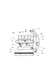
図1に本発明の電子写真感光ベルトを有する電子写真プロセスを利用したカラー画像形成装置(複写機あるいはレーザービームプリンター)の概略構成図を示す。
【0092】
図1において、1は第1の画像担持体として繰り返し使用される本発明のベルト状感光体であり、ローラー7、8によって張架され、矢印A方向に所定の速度(プロセススピード)で回転駆動される。感光ベルト1は、回転過程において、一次帯電手段2によりその周面に正または負の所定電位の均一帯電を受け、次いで、露光手段3(カラー原稿画像の色分解・結像露光光学系、画像情報の時系列電気デジタル画素信号に対応して変調されたレーザービームを出力するレーザースキャナによる走査露光系等)からの露光光4を受けることにより目的とするカラー画像の第1の色成分像(例えばイエロー色成分像)に対応した静電潜像が形成される。次いで、その静電潜像が第1の現像器(イエロー色現像器5Y)により第1色であるイエロートナーにより現像される。この時、第2〜第4の現像器(マゼンタ色現像器5M、シアン色現像器5C、ブラック色現像器5K)の各現像器は作動−オフになっていて感光ベルト1には作用せず、上記第1色のイエロートナー画像は上記第2〜第4の現像器により影響を受けない。
【0093】
10は中間転写ベルトであり、ローラー13、14によって張架され、矢印B方向に感光ベルト1と同じ速度をもって回転駆動されている。
【0094】
感光ベルト1上に形成担持された上記第1色のイエロートナー画像が、感光ベルト1と中間転写ベルト10とのニップ部を通過する過程で、1次転写ローラー9から中間転写ベルト10に印加される1次転写バイアスにより形成される電界により、中間転写ベルト10の外周面に順次中間転写(1次転写)されていく。
【0095】
中間転写ベルト10に対応する第1色のイエロートナー画像の転写を終えた感光ベルト1の表面は、クリーニング装置6により清掃される。
【0096】
以下、同様に第2色のマゼンタトナー画像、第3色のシアントナー画像、第4色のブラックトナー画像が順次中間転写ベルト10上に重ね合わせて転写され、目的のカラー画像に対応した合成カラートナー画像が形成される。
【0097】
11は2次転写ローラーで、中間転写ベルト10に対し離間可能な状態に配設してある。感光ベルト1から中間転写ベルト10への第1〜第4色のトナー画像の順次重畳転写のための1次転写バイアスは、トナーとは逆極性で、バイアス電源から印加される。その印加電圧は、例えば100V〜2kVの範囲である。
【0098】
感光ベルト1から中間転写ベルト10への第1〜第3色のトナー画像の1次転写工程において、2次転写ローラー11は中間転写ベルト10から離間することも可能である。
【0099】
中間転写ベルト10上に転写された合成カラートナー画像の最終画像担持体である転写材Pへの転写は、2次転写ローラー11が中間転写ベルト10に当接されると共に、記録媒体として複数枚の記録紙Pを積層収容してなる給紙カセット20から中間転写ベルト10と2次転写ローラー11との当接ニップに所定のタイミングで転写材Pが給送され、2次転写バイアスが電源28から2次転写ローラー11に印加される。この2次転写バイアスにより中間転写ベルト10から第2の画像担持体である転写材Pへ合成カラートナー画像が転写(2次転写)される。トナー画像の転写を受けた転写材Pは定着器15へ導入され加熱定着される。
【0100】
転写材Pへの画像転写終了後、中間転写ベルト10にはクリーニング用部材12が当接され、中間転写ベルト10の表面は、クリーニング装置12により清掃される。
【0101】
本発明においては、上述の電子写真感光体ベルト1、一次帯電手段2、現像手段5Y、5M、5C、5K及びクリーニング手段6等の構成要素のうち、複数のものをプロセスカートリッジとして一体に結合して構成し、このプロセスカートリッジを複写機やレーザービームプリンター等の電子写真装置本体に対して着脱自在に構成しても良い。
【0102】
図2は、本発明の電子写真感光ベルトを有する別の電子写真プロセスを利用したカラー画像形成装置(LEDプリンター)の概略構成図である。この方式は、中間転写体が不必要であり、また、光透過性(透明又は半透明)感光ベルトとLEDとを用いて、LED露光系を感光ベルト内面に設置することにより、小型化、低コスト化を実現できる方式である。この方式では、4組の帯電、露光、現像ユニットを具備することを特徴としており、感光ベルト上に、帯電、露光、現像を繰り返して、直接各色のトナー像を重ね合わせる画像形成方法である。このような、感光ベルト内部から露光する方法では、トナー層による光吸収と光散乱の影響がないため、潜像が忠実に再現できるという特徴をもつ。
【0103】
31は、本発明の透明感光体ベルトであり、ローラー39、40によって張架され、矢印C方向に所定の速度(プロセススピード)で回転駆動される。
【0104】
この方式では、感光体ベルト31の外周面側に一次帯電手段32Y、32M、32C、32K、現像器34Y、34M、34C、34BKが、感光体ベルト31の内周面側に露光手段33Y、33M、33C、33Kが、各々並設して構成されている。
【0105】
一次帯電器は、感光体ベルトと非接触であるコロナ帯電器を用いる。
【0106】
尚、現像器34Y、34M、34C、34BKにはそれぞれイエロー(Y)、マゼンタ(M)、シアン(C)、ブラック(BK)のトナーが収容されている。
【0107】
感光ベルト31は、回転過程において、カラー画像の第1の色成分像(図2においては、イエロー色成分像)のための一次帯電手段32Yによりその周面に正または負の所定電位の均一帯電を受け、次いで、LEDの露光手段33Y(カラー原稿画像の色分解・結像露光光学系、画像情報の時系列電気デジタル画素信号に対応して変調されたLED光を出力するLED)からの露光光(不図示)を受けることにより目的とするカラー画像の第1の色成分像(図2においては、イエロー色成分像)に対応した静電潜像が形成される。
【0108】
次いで、その静電潜像が第1の現像器(イエロー色現像器34Y)により第1色であるイエロートナーにより現像される。以下、同様に第2色のマゼンタトナー画像、第3色のシアントナー画像、第4色のブラックトナー画像が順次感光体ベルト31上に重ね合わせて現像され、目的のカラー画像に対応した合成カラートナー画像が形成される。
【0109】
感光ベルト1上に形成担持された上記合成カラートナー画像の、画像担持体である転写材Pへの転写は、転写ローラー35が感光体ベルト31に当接されると共に、給紙トレイ41から感光体ベルト31と転写ローラー35との当接ニップに所定のタイミングで転写材Pが給送され、転写バイアスが電源28から転写ローラー35に印加される。この2次転写バイアスにより感光体ベルト31から画像担持体である転写材Pへ合成カラートナー画像が転写される。トナー画像の転写を受けた転写材Pは定着器36へ導入され加熱定着される。
【0110】
転写材Pへの画像転写終了後、感光体ベルト31にはクリーニング用部材38が当接され、感光体ベルト31の表面は、クリーニング装置38により清掃される。
【0111】
前記方式の感光ベルトによるカラー画像形成装置は、感光ベルトを1回転させる間に各色画像が形成されるので、画像出力時間が非常に速いという利点がある。
【0112】
もちろん、本発明の感光ベルトは、ここに挙げたフルカラー電子写真装置以外にも、複数の感光ベルトを有するフルカラー電子写真装置や、モノクロの電子写真装置の感光ベルトとしても有効に活用できる。
【0113】
また、本発明の感光ベルトは、電子写真複写機、レーザービームプリンター、LEDプリンターに利用するのみならず、レーザー製版等電子写真応用分野にも広く用いることができる。
【0114】
本発明において、導電層を蒸着によって設けたシームレスベルト基体は、更にその上に感光層を設けることによって感光ベルトとして好適に用いられるが、導電層の電気抵抗値を適宜調整することにより、例えば、電子写真装置等の部品である中間転写ベルト、転写ベルト、紙搬送ベルト、定着ベルト等としても使用することもできる。
【0115】
【実施例】
以下、実施例をもって本発明を詳細に説明する。
【0116】
(実施例1)
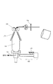
ポリエチレンテレフタレート樹脂(PET)のペレットを、図3に示される1軸押出し機100のホッパー120へ投入し、240〜280℃に加熱することにより溶融体とした。該溶融体は直径100mm、ダイギャップ800μmの環状ダイスに導かれ、該環状ダイスからチューブ状に押出されると同時に、空気導入路150より供給される圧縮空気によってチューブ160を膨張させた。膨張したチューブは、安定板170を通過した後、狭持部材としてのピンチロール180(ロールのニップ幅=600mm)を経て、折り径220mmで引き取られながら、長さ300mm毎にカッター190で、チューブ160の軸方向とほぼ直角方向に断続的に切断することで、ピンチロールに起因する折り目を有する円筒体を得た。得られた円筒体は、非常に平滑な表面を有するものであった。
【0117】
次に、この円筒体を加熱処理することにより、折り目の消去を行った。その後、幅を270mmに切り揃えて、ベルトを得た。なお、このベルトの周長は440mm、肉厚は100μmであった。
【0118】
図4のように、得られたシームレスベルト201を円筒治具202に装着し、これを更に、図5に示すような自転治具203に装着したものを、図6に示す真空蒸着装置のチャンバー内に入れ、チャンバー内をほぼ真空状態(気圧:10−4〜10−5Torr)とし、予め蒸発源205としてのタングステンからなるるつぼ型発熱体を発熱させ、該発熱体に仕込んでおいたアルミニウム(純度:99%以上)を蒸発させつつ、上記自転治具203を矢印D方向(逆方向でもかまわない)に自転させつつ、矢印E方向(逆方向でもかまわない)に公転させ、シームレスベルト201の外表面にアルミを蒸着させた。得られたアルミ蒸着膜の厚さは、500Å〜1500Åであった。
【0119】
得られたシームレスベルト基体上に、アルコール可溶性共重合ナイロン(商品名:アミランCM−8000、東レ(株)製)5部(質量部、以下同様)をメタノール95部に溶解した溶液を浸漬コーティング法により塗布し、80℃で10分間乾燥することによって、厚さが約1μmの下引層を形成した。
【0120】
次に、オキシチタニウムフタロシアニン顔料4質量部、ポリビニルブチラ−ル(商品名BX−1、積水化学工業(株)製)2質量部、シクロヘキサノン34質量部からなる混合溶液をサンドミルで10時間分散した後、テトラヒドロフラン60質量部を加えて電荷発生層用塗工液を調製した。この塗工液を前記中間層上に浸漬塗布し、100℃で10分間加熱乾燥し、膜厚0.2μmの電荷発生層を形成した。
【0121】
次に、電荷輸送物質として下記構造式で示されるトリアリ−ルアミン化合物47.5質量部
【0122】
【化1】

とポリカ−ボネ−ト樹脂(商品名ユ−ピロンZ200、三菱瓦斯化学(株)製)50質量部をクロルベンゼン400質量部に溶解して調製した溶液を前記電荷発生層上に浸漬塗布し、120℃で1時間加熱乾燥し、膜厚15μmの電荷輸送層を形成した。このときの電荷輸送物質の電荷輸送層を構成する物質全体に占める割合は、約48.7質量%である。
【0124】
上記のようにして、電子写真感光ベルトを作製した。
【0125】
感光層の未塗布部、すなわちアルミ蒸着面が剥き出しの部分に導電性テープを得られた感光ベルトの全周にわたって貼り付け、接地電極とした。
【0126】
作製した電子写真感光ベルトを図1に示される電子写真装置のうち、反転現像方式の電子写真装置に装着して、評価した。評価環境は、高温高湿(30℃、80%RH)、低温低湿(15℃、15%RH)下で行った。
【0127】
その結果、本実施例の電子写真感光ベルトは表1に示すように高温高湿及び低温低湿の何れの環境においても、暗部電位と明部電位との間に大きなコントラスト電位を得ることができた。さらに、連続して5000枚の通紙耐久による結果でも、電位変動はほとんどなく安定した特性を示している。また、高温高湿及び低温低湿の何れの環境においても、不要な黒点やカブリのないきれいな画像が得られた。
【0128】
(実施例2)
蒸着する金属をニッケルとした以外は、実施例1と同様にしてベルト感光体を得た。なお、蒸着されたニッケル膜の厚さは、1000〜1500Åであった。
【0129】
この感光体ベルトを実施例1と同様にして、電子写真装置に装着して評価した。
【0130】
その結果を表1に示す。
【0131】
(実施例3)
ニッケルを蒸着した後、更に銅を蒸着した以外は、実施例1と同様にしてベルト感光体を得た。なお、蒸着されたニッケル膜と銅膜の厚さは、合わせて1000〜1500Åであった。
【0132】
この感光体ベルトを実施例1と同様に同様にして、電子写真装置に装着して評価した。
【0133】
その結果を表1に示す。
【0134】
(実施例4)
実施例1と同様にしてシームレスベルトを得た。このシームレスベルト上に導電層として、厚さ約1μmのITO蒸着層を設けた。これに、実施例1と同様にして感光層を設け、シームレス感光ベルトを得た。この感光ベルトのLED光に対する光透過率は85%であった。この感光体ベルトを図2に示す電子写真装置に装着して評価した。
【0135】
その結果、本実施例の電子写真感光ベルトは表1に示すように高温高湿及び低温低湿の何れの環境においても、暗部電位と明部電位との間に大きなコントラスト電位を得ることができた。さらに、連続して5000枚の通紙耐久による結果でも、電位変動はほとんどなく安定した特性を示している。また、高温高湿及び低温低湿の何れの環境においても、不要な黒点やカブリのないきれいな画像が得られた。
【0136】
(比較例1)
感光ベルト基体として、カーボンブラックを分散したポリイミドを遠心成形したもの(体積抵抗率7×10³Ω・cm、厚さ70μm)を使用し、この上に実施例1と同様にして感光層を設け、電子写真感光体ベルトを作製した。得られた感光ベルトを実施例1と同様にして、電子写真装置に装着して評価した。
【0137】
その結果、高温高湿及び低温低湿の何れの環境においても、暗部電位は低く、明部電位は高めであり、画像形成に必要な十分なコントラスト電位を得ることができなかった。
【0138】
また、高温高湿及び低温低湿の何れの環境においても、カブリの多い、質の悪い画像しか得られなかった。よって本比較例では、連続通紙を行わなかった。
【0139】
(比較例2)
感光ベルト基体として、実施例1で得られたPET製のシームレスベルトに、カーボンブラック30部をポリウレタン70部に分散したコーティング剤を塗布したものを使用し、感光層は実施例1と同様にして電子写真感光体ベルトを作製した。得られた感光ベルトを実施例1と同様にして、電子写真装置に装着して評価した。
【0140】
その結果、高温高湿及び低温低湿の何れの環境においても、暗部電位は低く、明部電位は高めであり、画像形成に必要な十分なコントラスト電位を得ることができなかった。
【0141】
また、高温高湿及び低温低湿の何れの環境においても、カブリの多い、質の悪い画像しか得られなかった。よって本比較例では、連続通紙を行わなかった。
【0142】
(比較例3)
感光ベルト基体として、ポリエチレンテレフタレート75部にカーボンブラック25部を分散混練したものをシームレスベルト状に押出し成形したものを用い、感光層は実施例1と同様にして電子写真感光体ベルトを作製した。得られたシームレスベルトの体積抵抗値は2×10⁷Ω・cmであった。
【0143】
得られた感光ベルトを実施例1と同様にして、電子写真装置に装着して評価した。
【0144】
その結果、高温高湿及び低温低湿の何れの環境においても、暗部電位は低く、明部電位は高めであり、画像形成に必要な十分なコントラスト電位を得ることができなかった。
【0145】
また、高温高湿及び低温低湿の何れの環境においても、カブリの多い、質の悪い画像しか得られなかった。よって本比較例では、連続通紙を行わなかった。
【0146】
(比較例4)
実施例1で用いた、導電層が設けられたシームレスベルト基体に、電荷輸送物質を55質量部にした以外は実施例1と同様にしてシームレス感光ベルトを得た。
【0147】
得られた感光ベルトを実施例1と同様にして、電子写真装置に装着して評価した。
【0148】
その結果、感光層にクラックが発生し、実用に耐えないものであった。
【0149】
【表1】
【発明の効果】
以上に説明したように本発明の電子写真感光ベルトは、感光体として必要な導電性を安定して得ることができ、画像欠陥がなく、耐久性に優れ、しかも安価に製造可能なものである。
【図面の簡単な説明】
【図1】本発明のシームレス感光ベルトを用いた電子写真装置の概略図である。
【図2】本発明のシームレス感光ベルトを用いた、また別の電子写真装置の概略図である。
【図3】本発明のシームレス感光ベルトの基体であるシームレスベルトの成形機を示す概略図である。
【図4】シームレスベルトを円筒治具に取り付けた図である。
【図5】シームレスベルトが取り付けられた円筒治具を、自転治具に取り付けた図である。
【図6】本発明における蒸着装置の概略図である。
【符号の説明】
1 感光ベルト
2 一次帯電手段
3 露光手段
4 露光光
5Y イエロー色現像器
5M マゼンタ色現像器
5C シアン色現像器
5K ブラック色現像器
6 クリーニング装置
7、8 ローラー
9 1次転写ローラー
10 中間転写ベルト
11 2次転写ローラー
12 クリーニング用部材
13、14 ローラー
15 定着器
20 給紙カセット
31 感光ベルト
32Y イエロー一次帯電手段
32M マゼンタ一次帯電手段
32C シアン一次帯電手段
32K ブラック一次帯電手段
33Y イエローLED露光手段
33M マゼンタLED露光手段
33C シアンLED露光手段
33K ブラックLED露光手段
34Y イエロー色現像器
34M マゼンタ色現像器
34C シアン色現像器
34K ブラック色現像器
35 転写ローラー
36 定着器
38 クリーニング装置
39、40 ローラー
41 給紙カセット
100 1軸押出し機
120 ホッパー
150 空気導入路
160 チューブ
170 安定板
180 ピンチロール
190 カッター
201 シームレスベルト
202 円筒治具
203 自転治具
204 真空蒸着装置
205 蒸着源
P 転写材[0001]
TECHNICAL FIELD OF THE INVENTION
The present invention relates to a seamless photosensitive belt, and more particularly, to a method for manufacturing a seamless photosensitive belt, a process cartridge having the seamless photosensitive belt, and an electrophotographic apparatus.
[0002]
[Prior art]
The electrophotographic photosensitive member is a core of an electrophotographic apparatus and is indispensable for an image forming apparatus using an electrophotographic method. An electrophotographic photosensitive member basically includes a photosensitive layer for forming a latent image by charging and exposure using light, and a base on which the photosensitive layer is provided.
[0003]
At present, many electrophotographic photoconductors are generally provided in the form of a drum such as an aluminum cylinder, and there are many copying machines and printers equipped with a drum-shaped photoconductor in the market.
[0004]
On the other hand, there is an electrophotographic apparatus using a flexible belt-shaped photoconductor. The advantage of the belt-shaped photoreceptor is that by taking advantage of its excellent flexibility, the process around the photoreceptor, such as charging, exposure, development, transfer, and cleaning, is relatively arbitrarily arranged for image formation. It is a point that it becomes possible. Due to this advantage, the size of the electrophotographic apparatus can be reduced. The downsizing of the device also has the advantage of reducing the cost of the device itself.
[0005]
Since the photosensitive belt is flexible and can take any shape, there is a great merit in the process design, such as a large nip adjustment range in the transfer and development areas.
[0006]
In addition, the photosensitive belt has an advantage that the life can be extended by increasing the loop length. Further, since a relatively large plane portion can be formed by increasing the loop length, the entire surface of the flash can be exposed, and there is a possibility that the speed of the electrophotographic apparatus can be sufficiently satisfied.
[0007]
Further, in the case of the photosensitive belt, it is easy to make the substrate transparent or translucent (light transmitting) as compared with the photosensitive drum. In this case, the exposing means is arranged on the inner peripheral surface side of the photosensitive belt. In addition, a system for exposing from the back of the photosensitive belt can be used, and the size of the electrophotographic apparatus can be significantly reduced.
[0008]
Further, by making the photosensitive belt translucent, there is an advantage that charges can be eliminated by irradiating light from the back surface (inner peripheral surface) side.
[0009]
In the case of a full-color copying machine or a full-color printer, four developing units are required. However, in the case of a photosensitive belt, these developing units are arranged at arbitrary positions because of their excellent flexibility. It is suitable for full-color copying machines and full-color printers.
[0010]
Due to such advantages, color copiers and color printers using a photosensitive belt as a photoreceptor have already started operating in the market.
[0011]
As a photosensitive belt used in a conventional electrophotographic apparatus, the following two types are in practical use.
[0012]
For example, as described in Japanese Patent Application Laid-Open No. 10-186701, a photosensitive layer is applied and formed on a resin film (for example, a polyester film) on which aluminum is deposited, and then cut into predetermined dimensions. This is annularly joined by ultrasonic welding or the like to form a belt shape. This method has an advantage that it can be generally manufactured at low cost. However, in such a manufacturing method, it is inevitable that a joint is left at a joint portion. If an image is written in this joint, the joint will appear in the image as it is, resulting in an image defect. In order to avoid such a situation, it is necessary to form a latent image while avoiding the seam portion. For this purpose, a mechanism for sensing and avoiding the seam portion is required. Providing such a mechanism is not preferable because the machine cost increases. In addition, the presence of the joint causes a shock when the roll passes, or a shock when the joint at the time of blade cleaning passes the blade causes color shift and the like, which is not preferable. Further, the photosensitive belt has a limitation that the circumference of the electrophotographic apparatus having the photosensitive belt must be equal to or larger than the maximum paper size. As a result, there is a problem that the apparatus becomes large.
[0013]
In order to solve these seam problems, for example, Japanese Patent Application Laid-Open No. 08-030001 and Japanese Patent Application Laid-Open No. 08-146635 have been proposed. In addition to the cost increase, the joint step can be reduced by these methods, but the essential problem of the existence of the joint has not been solved.
[0014]
The other is to apply a photosensitive layer on a seamless conductive substrate (photoreceptor substrate) obtained by electroforming nickel to form a photoreceptor belt, as disclosed in JP-A-63-127249. It was done. With this method, the problem of the joint can be avoided, but the mass production equipment by electric casting is large-scale, and it takes a very long time to obtain a desired thickness with high accuracy, and the cost is high. is there. In addition, when trying to have mechanical strength that can be used as a belt, a thick film is inevitably formed, resulting in poor flexibility and a problem in practicality. In addition, there is also a demerit that exposure from the inner surface of the belt becomes impossible because transparency is completely lost.
[0015]
Therefore, there is a strong demand for the development of a seamless photosensitive belt that uses a so-called seamless belt as a photosensitive member substrate, which is made of a resin and has no seams. A photosensitive belt made of a resin has been obtained by the following molding method. Means have been proposed.
[0016]
A polyimide solution is cast-formed (centrifugally formed) on a rotating drum, imidized and cured to produce a seamless belt as a photoreceptor substrate, and then a conductive layer, a photosensitive layer, and the like are applied to the seamless belt. thing.
[0017]
On the other hand, a thermoplastic resin (for example, a polyester resin) is extruded from an annular die to produce a seamless belt as a photoreceptor substrate, and a conductive layer, a photosensitive layer and the like are coated thereon.
[0018]
However, the above-described photoreceptor belt requires a step of applying a conductive layer to the seamless belt, which is a problem in that the process is complicated and lowers productivity, and the resistance of the coating agent to be applied is reduced to a resistance required for the photoreceptor. It is difficult to lower the resistance, and even if the reduction is possible, there is a problem that the resistance value itself varies.
[0019]
As described above, the type in which the conductive layer is provided by coating is not preferable because the resistance of the coating material, the resistance unevenness, and the coating cost increase. Further, when a solvent-based paint is used as the conductive layer paint, the residual solvent may attack the photosensitive layer and cause image abnormalities.
[0020]
As another method, for example, a photosensitive layer or the like is applied to a seamless conductive belt (photoreceptor substrate) obtained by casting (centrifugally forming) a polyimide dispersion liquid in which a conductive filler such as conductive carbon black is previously mixed and dispersed. What constitutes it.
[0021]
For the photoreceptor belt described above, since the conductive filler is dispersed in the solvent, the conductive filler easily moves in the solvent, and it is difficult to uniformly control the dispersion of the conductive filler. Thus, the electric resistance value varies.
[0022]
Therefore, when a photosensitive layer is applied to the seamless conductive belt and used as a photosensitive belt, there is a problem that image unevenness occurs. Furthermore, since the seamless belt is made using a solvent, the residual solvent may attack the photosensitive layer and cause image abnormalities.
[0023]
In addition, for example, as disclosed in Japanese Patent Application Laid-Open No. 02-233765, a seamless conductive belt (photoconductor) in which a thermoplastic resin containing a conductive filler such as carbon black is extruded from a circular die into a thermoplastic resin such as polyester or polycarbonate A structure in which a conductive layer, a photosensitive layer, or the like is applied to a substrate is proposed.
[0024]
In the above method, the productivity is excellent because of continuous molding, but a large amount of conductive filler such as carbon black must be mixed with an insulating resin in order to make the conductive region necessary for the photoreceptor. It is difficult for the dispersion of the conductive filler to be uniform, and the electric resistance value is likely to vary, possibly resulting in image irregularities of unknown cause. In addition, since a large amount of conductive filler such as carbon black must be added to develop conductivity, the strength of the resin itself is reduced, and the belt is easily broken and used as a photosensitive belt. I didn't.
[0025]
In addition, for example, Japanese Patent Publication No. 04-078990 describes that a conductive layer is provided by vapor deposition. This method has a strong adhesion to a substrate and is a preferred method.
[0026]
On the other hand, the electrophotographic photosensitive belt is usually stretched between a plurality of rollers and used in an electrophotographic apparatus such as a copying machine or a printer by rotating and driving the belt. While these electrophotographic devices are used repeatedly, the photosensitive belt cracks in the photosensitive layer due to the bending that occurs repeatedly when passing around the roller and the tension that exists between the rollers, and the photosensitive belt as a photosensitive belt There is a problem that the bending resistance is not sufficient. Cracks are most likely to occur in the charge transport layer among the photosensitive layers, and the configuration of the charge transport layer is a very large factor that affects the durability of the photosensitive belt.
[0027]
The above-mentioned Japanese Patent Publication No. 04-078990 has an advantage that a stable electric resistance value can be obtained without a seam. However, the ratio of the charge transport material to the binder resin in the photosensitive layer, particularly the charge transport layer, is set to 1: 1. Since the charge transport material is contained in a large amount, it is excellent in charge mobility. On the other hand, when the amount of these charge transporting substances is increased, not only is the film-forming property inferior, but also cracks are liable to occur when used as a photosensitive belt, which is not practical.
[0028]
A photosensitive belt is composed of a belt base, a conductive layer, and a photosensitive layer, and can only be put to practical use as a photosensitive belt when it satisfies each function. The appearance of such a photosensitive belt is desired. Was.
[0029]
[Problems to be solved by the invention]
SUMMARY OF THE INVENTION An object of the present invention is to solve the above-described various problems, to stably obtain the conductivity required for a photoconductor, to eliminate image defects, to have excellent durability, and to be able to manufacture a photoconductor at a low cost. To get the belt.
[0030]
[Means for Solving the Problems]
That is, a seamless photosensitive belt having at least a conductive layer and a charge transport layer on a seamless belt, wherein the conductive layer is formed by vapor deposition, the charge transport layer contains at least a charge transport material, and the charge transport layer The object of the present invention is attained by a seamless photosensitive belt in which the ratio of the charge transporting substance to the whole constituting substance is less than 50% by mass.
[0031]
BEST MODE FOR CARRYING OUT THE INVENTION
Next, the present invention will be described in more detail.
[0032]
In the present invention, it is premised that the belt serving as the base of the photosensitive belt has no seam, that is, a so-called seam. If there is no seam, any belt can be used as the base of the photosensitive belt. In the present invention, the seamless belt refers to a cylindrical member having flexibility, and is not particularly limited as long as it has a belt shape.
[0033]
The material of the seamless belt in the present invention may be any material. Examples include, but are not limited to, organic materials, inorganic compounds, composites thereof, rubbers such as thermosetting resins, thermoplastic resins, and other various materials. For reasons such as ease of molding, a thermosetting resin or a thermoplastic resin is preferably used.
[0034]
More specifically, polyethylene (high density, medium density, low density, linear low density, etc.), polypropylene, polystyrene, ethylene-vinyl alcohol copolymer (EVOH), polycarbonate, polyamide, polyacetal, polyarylate, polyphenylene Ether, modified polyphenylene ether, polyimide, liquid crystal polymer, polysulfone, polyether sulfone, polyphenylene sulfite, polybisamide triazole, polyetherimide, polyamideimide, polyetheretherketone, aliphatic polyketone, polymethylpentene, polybutyleneterephthalate , Polyethylene terephthalate, polyethylene naphthalate, polyvinyl fluoride, polyvinylidene fluoride, chlorotrifluoroethylene, hexafluoropropylene, Perfluoroalkyl vinyl ether copolymer, it is possible to use one kind or two or more kinds of methacrylic resins, selected from such various other copolymers.
[0035]
Also, any additives may be added to these resins. Specific examples include fillers such as talc, mica, and calcium carbonate; flame retardants such as magnesium hydroxide and antimony trioxide; and antioxidants (phenol-based, sulfur-based, and the like). Of course, the additives are not limited to the above substances, and any other additives can be used.
[0036]
As a method of adding the above-mentioned additives to the above-mentioned resin if desired, a method of performing pre-mixing, followed by kneading using a known kneading machine such as a single-screw extruder, a twin-screw extruder, a Banbury mixer, a roll, and a kneader. No. Normally, each component is kneaded with an extruder or the like to form a pellet-shaped compound and then molded.However, in special cases, each component is directly supplied to the molding machine and the composition is kneaded with the molding machine. It can also be formed while molding.
[0037]
In particular, in the present invention, when obtaining a light-transmissive photosensitive belt, it is necessary to use a light-transmissive material, among the above-listed materials and other materials, particularly excellent in light-transmittance, For example, those polymerized using methacrylic acid methyl ester monomer are the best in light transmission, strength, precision, surface properties, etc., but other polyethyl methacrylate, polybutyl methacrylate, polyethyl acrylate, polybutyl acrylate , Polystyrene, polyimide, polyester, polyvinyl chloride, or the like, or a copolymer thereof, or the like. Further, polybutylene terephthalate (PBT), polyethylene terephthalate (PET), polyphenylene sulfide (PPS), nylon and the like can also be used sufficiently.
[0038]
In particular, it is preferable to use polyethylene terephthalate (PET) or the like.
[0039]
In the present invention, when a light-transmitting photosensitive belt is obtained, the light transmittance of the seamless belt is desirably 50% or more. If it is less than 50%, the light transmittance is poor, the light energy required for backside exposure becomes large, the exposure system becomes large, and a large amount of energy is required, resulting in an increase in size and cost of the apparatus. It is not preferable.
[0040]
As a manufacturing method of the seamless belt in the present invention, any manufacturing method that does not allow seam can be selected. For example, known methods such as a centrifugal molding method, an injection molding method, a blow molding method, a continuous melt extrusion molding method, and an inflation molding method can be employed. Above all, extrusion from an annular die is preferable since continuous molding is possible and production can be performed at lower cost.
[0041]
Further, the obtained seamless belt may be subjected to a treatment such as annealing or an operation such as stretching. Further, heat treatment or the like may be performed to stabilize the dimensions. A particularly preferable heat treatment method is a method in which an inner mold and an outer mold are used, a seamless belt is provided therebetween, and heating is performed. This treatment is preferable because folds generated by the inflation molding method can be eliminated, and at the same time, dimensional stability and surface smoothness can be achieved.
[0042]
In the present invention, a seamless belt is used as a substrate of the photosensitive belt, but a sheet-like material that is not cylindrical is rolled and joined, and a seam is eliminated to the extent that defect guiding means does not substantially occur in an image. (Even if the belt is formed by connecting films, if there is no substantial seam, it can be used as the belt in the present invention).
[0043]
The thickness of the seamless belt is preferably from 50 to 1000 μm, more preferably from 100 to 700 μm. When the thickness is less than 50 μm, the belt is easily stretched, and when the thickness exceeds 1000 μm, it becomes difficult to flexibly deform the belt.
[0044]
The seamless belt of the present invention may be composed of a single layer, or may be composed of a plurality of layers. When obtaining a seamless belt composed of a plurality of layers, a thermoplastic resin member previously formed of a plurality of layers may be obtained by extrusion from a multilayer die, or a single-layer seamless belt may be obtained from a single-layer thermoplastic resin member. Thereafter, a new layer may be provided on the front surface or the back surface of the single-layer seamless belt (for example, spraying or dipping of paint or the like) to obtain a seamless belt having a plurality of layers.
[0045]
In the case of an electrophotographic apparatus using coherent light such as a laser beam as an exposure light source, interference fringes may occur. When the substrate of the photoreceptor is transparent, such a problem does not occur because light rays emitted from a light source are transmitted. And interference fringes may occur. In such a case, the surface of the support may be roughened to an appropriate surface roughness in advance.
[0046]
When a seamless belt is used as a photosensitive belt, a conductive layer is required. In the present invention, the conductive layer of the seamless photosensitive belt is provided by vapor deposition. The vapor deposition in the present invention is to heat and evaporate metals, metal oxides, ceramics, and other substances in a high vacuum state, and adhere the generated vapor to the surface of a target substance (in the case of the present invention, a seamless belt). Needless to say, it is essentially different from dipping or spray coating.
[0047]
As a method for vapor deposition, any of a PVD method (Physical Vapor Deposition, physical vapor deposition method) and a CVD method (Chemical Vapor Deposition, chemical vapor deposition method) can be adopted.
[0048]
Specifically, a vacuum evaporation method, a sputtering method (DC sputtering method, high frequency sputtering method, reactive high frequency sputtering method, etc.), an ion plating method, a high frequency ion plating method, an ion beam sputtering method, an ion beam assist method, a glow Any of conventionally known methods such as a discharge method, a metal spraying method, a molecular beam epitaxy method (MBE method), a plasma CVD method, an ion cluster beam method, and plating can be employed, but the method is not limited thereto. Moreover, you may use combining the method mentioned here.
[0049]
The above-described deposition method is a very suitable method for obtaining a very thin film uniformly.
[0050]
Among the above-described vapor deposition methods, a sputtering method, an ion plating method, a high-frequency ion plating method, and the like are preferable because of high adhesion to a substrate.
[0051]
As a material to be evaporated by heating and evaporating, that is, a material for forming a conductive layer in the present invention, a known metal, metal oxide, or the like can be used.
[0052]
Specifically, as a material used for the conductive layer, for example, aluminum (Al), gold (Au), silver (Ag), copper (Cu), nickel (Ni), titanium (Ti), zinc (Zn), chromium ( Cr), indium (In), tin (Sn), lead (Pb), iron (Fe), zirconium (Zr), bismuth (Bi), cadmium (Cd), antimony (Sb), tantalum (Ta), cerium ( Ce), neodymium (Nd), lanthanum (La), thorium (Th), magnesium (Mg), gallium (Ga), tungsten (W), molybdenum (Mo), silicon (K), platinum (Pt), palladium ( Pd), one or more metals selected from cobalt (Co), or a mixture thereof, and at least one selected from alloys, oxides, nitrides, sulfides, and composite compounds thereof. It can be mentioned. Of course, it is needless to say that materials other than the metals listed here may be used. Among them, aluminum is preferable because it is inexpensive and vaporizes at a relatively low temperature.
[0053]
Further, the above-described metal may be used as a single layer, or one or more layers may be further provided thereon to form a multilayer film.
[0054]
In the present invention, particularly when a light-transmitting photosensitive belt is to be obtained, a light-transmitting conductive layer is necessary. As a material of the light-transmitting conductive layer, a known metal oxide or the like can be applied.
[0055]
Specifically, for example, SnO 2 , CdO, ZnO, CTO (CdSnO 3 , Cd 2 SnO 4 , CdSnO 4 ), In 2 O 3 , CdIn 2 O 4 And the like. Preferably, it is a composite (doped) phase in which one or more selected from Sn, Sb, F and Al are added to the above metal oxide. Among them, preferred is In to which Sn is added. 2 O 3 (Indium-Tin-Oxide, ITO), SnO with Sb added 2 , F-added SnO 2 , And ZnO to which Al is added. These layers can be used in a single layer or in multiple layers.
[0056]
Among them, ITO can be suitably used because, in addition to transparency and refractive index, ITO has a high film forming speed and good adhesion to a substrate.
[0057]
When a light-transmitting conductive layer is obtained, the above-described metal such as Al, Au, or Cu is formed thin enough to be translucent, without using a transparent metal oxide as described above. A conductive layer may be used.
[0058]
In the present invention, when a light-transmitting photosensitive belt is obtained, the light-transmitting property of the conductive layer is desirably 50% or more. If it is less than 50%, the light transmittance is poor, the light energy required for backside exposure becomes large, the exposure system becomes large, and a large amount of energy is required, resulting in an increase in size and cost of the apparatus. It is not preferable.
[0059]
The conductive layer of the present invention usually has a surface resistance of 10 6 Ω / □ or less, especially 10 4 Ω / □ or less is preferable. Surface resistance is 10 6 If it exceeds Ω / □, the charging current at the time of charging the photosensitive belt is insufficient, resulting in poor charging, and the photocurrent at the time of light irradiation being insufficient, resulting in poor sensitivity. In addition, it often causes an increase in the residual potential of the photoconductor, which deteriorates the repetition characteristics.
[0060]
The thickness of the conductive layer is usually preferably about 100 to 50,000 °. More preferably, it is about 500 to 10000 °.
[0061]
If the angle is less than 100 °, the light transmittance is high, but the deposited film tends to be a discontinuous film and the conductivity is insufficient. On the other hand, if it exceeds 50,000 °, the conductivity is high, but it is difficult to follow the bending of the seamless belt as the base material, and the bending resistance deteriorates. Further, when the exposure is performed from the inner surface of the photosensitive belt, if the film thickness is too large, the light transmittance is reduced, which is not preferable.
[0062]
The surface of the seamless belt to be vapor-deposited is subjected to etching treatment such as corona discharge treatment, glow discharge treatment, flame treatment, ultraviolet irradiation, electron beam irradiation, or primer treatment, or a conductive layer formed on the surface of the seamless belt. A treatment for improving the adhesion may be performed. Among them, corona discharge treatment is most preferably used because of its easy handling and relatively stable treatment strength. Before forming the conductive layer, dust-proofing such as solvent cleaning or ultrasonic cleaning may be performed as necessary.
[0063]
In the present invention, as a device for performing vapor deposition, a known device can be used as long as it has a chamber that can sufficiently accommodate a seamless belt to be vapor-deposited.
[0064]
When performing vacuum vapor deposition, the vapor deposition film tends to be thicker near the vapor deposition source, and thinner at a position farther from the vapor deposition source, which tends to cause unevenness in film thickness. In order to solve this problem, it is preferable to rotate the support to be deposited. In the rotation, it is preferable to revolve around the evaporation source while rotating around the evaporation source, since the film thickness unevenness can be minimized and a more uniform thin film can be formed.
[0065]
In the present invention, when a light-transmitting photosensitive belt is obtained, the light transmittance of the seamless belt provided with the conductive layer is desirably 50% or more. If it is less than 50%, the light transmittance is poor, the light energy required for backside exposure becomes large, the exposure system becomes large, and a large amount of energy is required, resulting in an increase in size and cost of the apparatus. It is not preferable.
[0066]
Next, the photosensitive layer of the electrophotographic photosensitive belt used in the present invention will be described.
[0067]
Normally, the photosensitive layer is composed of a single layer containing both a charge generating substance and a charge transporting substance in the same layer, and a charge generating layer containing a charge generating substance and a charge transporting layer containing a charge transporting substance. It is broadly classified into a stacked type (separated type). The constitution of the photosensitive layer of the present invention is classified into the latter type.
[0068]
The structure of the photosensitive layer of the present invention includes a charge-generating layer and a charge-transporting layer laminated in this order on a seamless belt substrate provided with a conductive layer, and a charge-transporting layer and a charge-generating layer laminated in this order. There is.
[0069]
The charge generation layer will be described. As the charge generating substance, azo pigments such as Sudan Red, Diane Blue, and Genus Green B, quinone pigments such as Argol yellow, pyrene, quinone, anthantrone, indanthrene brilliant violet RRP, quinocyanine pigments, perylene pigments, indigo, Indigo pigments such as thioindigo, bisbenzimidazole pigments such as India First Orange Toner, phthalocyanine pigments such as copper phthalocyanine, titanyl phthalocyanine, gallium phthalocyanine and aluminum chloro-phthalocyanine, quinacridone pigments and azulene described in Japanese Patent Application No. 57-165263. Compounds and the like, and at least one of these substances may be used as polyester, polystyrene, polyvinyl butyral, polyvinyl pyrrolidone, methyl cellulose, , Polyacrylic acid esters, cellulose esters, and dispersed in at least one or more binder resin selected from polyvinyl acetate and acrylic resin or the like to obtain a dispersion. The obtained dispersion is applied to a seamless belt provided with a conductive layer or a seamless belt provided with a barrier layer and a conductive layer, and dried to obtain a charge generation layer. The charge generation material is formed by vapor deposition. As the vapor deposition method, the method for vapor deposition of the conductive layer described above can be applied as it is.
[0070]
The thickness of the charge generation layer is 5 μm or less, preferably 0.01 to 3 μm, more preferably 0.01 to 1 μm, and still more preferably 0.05 to 0.5 μm.
[0071]
Next, the charge transport layer will be described. The charge transport layer is a polycyclic aromatic compound having a structure such as biphenylene, anthracene, pyrene, phenanthrene, or coronene in the main chain or side chain, indole, carbazole, oxazole, isoxazole, thiazole, imidazole, pyrazole, oxadiazole, and pyrazoline. A solution in which at least one or more charge transporting substances (hole transporting substances) selected from compounds having a nitrogen-containing cyclic compound such as thiadiazole and triazole, hydrazone compounds and styryl compounds are dissolved in a resin having a film-forming property. Is formed by coating and drying. This is because the charge-transporting substance generally has a low molecular weight, and itself has poor film-forming properties. Examples of such resin include at least one resin selected from polycarbonate, polymethacrylates, polyarylate, polystyrene, polyester, polysulfone, styrene-acrylonitrile copolymer, styrene-methyl methacrylate copolymer, and the like.
[0072]
In the present invention, the ratio of the above-described charge transporting substance (hole transporting substance) to the whole substance constituting the charge transporting layer needs to be less than 50% by mass. If the proportion of the charge transporting substance in the whole substance constituting the charge transporting layer is 50% by mass or more, film formability is poor and cracks are easily generated when used as a photosensitive belt, which is not preferable. There is no particular limitation as long as it is less than 50% by mass, but preferably 49.5% by mass or less, more preferably 49% by mass or less. In the present invention, if the amount is less than 50% by mass, the lower limit is not particularly set. However, if the amount is extremely small, the photosensitive characteristics deteriorate.
[0073]
The thickness of the charge transport layer is preferably 5 to 40 μm, more preferably 10 to 30 μm.
[0074]
Further, in the present invention, a barrier layer having a barrier function and an adhesive function may be provided between the conductive layer and the photosensitive layer (charge generation layer, charge transport layer) provided on the seamless belt, if necessary. The barrier layer can be formed of casein, polyvinyl alcohol, nitrocellulose, ethylene-acrylic acid copolymer, polyamide (nylon 6, nylon 66, nylon 610, copolymer nylon, alkoxymethylated nylon, etc.), polyurethane, gelatin, and the like.
[0075]
The thickness of the barrier layer is preferably 0.05 to 5 μm, and more preferably 0.3 to 1 μm.
In the invention, a protective layer may be further provided on the photosensitive layer.
[0076]
Examples of the material constituting the protective layer include polyester, polyacrylate, polyethylene, polystyrene, polybutadiene, polycarbonate, polyamide, polypropylene, polyimide, polyamideimide, polysulfone, polyacrylether, polyacetal, phenol, acrylic, silicone, epoxy, urea, and allyl. Alkyd, butyral, phenoxy, phosphazene, acrylic-modified epoxy, acrylic-modified urethane, and acrylic-modified polyester resin.
[0077]
The thickness of the protective layer is preferably from 0.2 to 10 μm.
[0078]
When the image input is light having a single wavelength, such as laser light, such as a laser beam printer (LBP), a second conductive layer is provided for the purpose of preventing interference fringes due to scattering or covering a scratch on the substrate. You may. This can be formed by dispersing conductive powder such as carbon black, metal particles, and metal oxide particles in a binder resin. The thickness of the second conductive layer is preferably 5 to 40 μm, and more preferably 10 to 30 μm.
[0079]
The second conductive layer refers to a conductive layer provided further on a seamless belt on which a conductive layer has already been provided by vapor deposition.
[0080]
In each of the above layers, polytetrafluoroethylene, polyvinylidene fluoride, a fluorine-based graft polymer, a silicone-based graft polymer, a fluorine-based block polymer, a silicone-based block polymer, and a silicone-based block copolymer are used to improve cleaning properties and abrasion resistance. A lubricant such as a system oil may be contained.
[0081]
Further, additives such as an antioxidant may be added for the purpose of improving the weather resistance.
[0082]
In addition, a conductive powder such as conductive tin oxide and conductive titanium oxide may be dispersed in the protective layer for the purpose of controlling resistance.
[0083]
Known methods can be used as a method for applying each of these layers applied in the present invention, such as a dip coating method, a spray coating method, a beam coating method, a spinner coating method, and a spin coating method. -A coating method, a myrbar coating method, a blade coating method, a gravure coating method and the like.
[0084]
In particular, in the present invention, the immersion coating method is suitable in view of the shape of the support.
[0085]
In the present invention, when a light-transmissive photosensitive belt is obtained, the light transmittance of the seamless belt provided with the conductive layer and the photosensitive layer is desirably 50% or more. If it is less than 50%, the light transmittance is poor, the light energy required for backside exposure becomes large, the exposure system becomes large, and a large amount of energy is required, resulting in an increase in size and cost of the apparatus. It is not preferable.
[0086]
In the photosensitive belt, the inner diameter accuracy of the belt is very important, and if it is bad, the photosensitive belt meanders, which is not preferable. A preferred range is a range of the variation within ± 0.5% with respect to the average value of the inner diameter.
[0087]
Further, if the thickness of the photosensitive belt is uneven, the image becomes uneven, which is not preferable. A preferred range is a range where the thickness variation is within ± 5%.
[0088]
For the seamless photosensitive belt described so far, a tape-like reinforcing member made of polyester or the like is attached to the end of the photosensitive belt in order to prevent end cracking, chipping, scraping, etc., and improve durability. It may be provided.
[0089]
Further, for the purpose of preventing the photosensitive belt from meandering, a meandering preventing member made of, for example, polyurethane or the like may be provided at the rear end of the photosensitive belt.
[0090]
In addition, a conductive tape or the like may be provided at an end of the photosensitive belt for the purpose of energizing the conductive layer.
[0091]
FIG. 1 is a schematic configuration diagram of a color image forming apparatus (copier or laser beam printer) using an electrophotographic process having the electrophotographic photosensitive belt of the present invention.
[0092]
In FIG. 1, reference numeral 1 denotes a belt-shaped photoconductor of the present invention which is repeatedly used as a first image carrier, is stretched by
[0093]
[0094]
The first color yellow toner image formed and carried on the photosensitive belt 1 is applied from the
[0095]
After the transfer of the first color yellow toner image corresponding to the
[0096]
Hereinafter, similarly, the magenta toner image of the second color, the cyan toner image of the third color, and the black toner image of the fourth color are sequentially superimposed on the
[0097]
[0098]
In the primary transfer process of the toner images of the first to third colors from the photosensitive belt 1 to the
[0099]
The transfer of the composite color toner image transferred on the
[0100]
After the image transfer to the transfer material P is completed, the cleaning
[0101]
In the present invention, among the above-described components such as the electrophotographic photoreceptor belt 1, the
[0102]
FIG. 2 is a schematic configuration diagram of a color image forming apparatus (LED printer) using another electrophotographic process having the electrophotographic photosensitive belt of the present invention. This method does not require an intermediate transfer member, and uses a light-transmissive (transparent or translucent) photosensitive belt and an LED to install an LED exposure system on the inner surface of the photosensitive belt, thereby reducing the size and cost. This is a method that can realize cost reduction. This method is characterized by having four sets of charging, exposing, and developing units, and is an image forming method in which charging, exposing, and developing are repeated on a photosensitive belt to directly superimpose toner images of respective colors. Such a method of exposing from the inside of the photosensitive belt has a feature that a latent image can be faithfully reproduced because there is no influence of light absorption and light scattering by the toner layer.
[0103]
[0104]
In this method,
[0105]
The primary charger uses a corona charger that is not in contact with the photoreceptor belt.
[0106]
The developing
[0107]
In the course of rotation, the
[0108]
Next, the electrostatic latent image is developed by the first developing device (yellow
[0109]
The transfer of the composite color toner image formed and carried on the photosensitive belt 1 onto a transfer material P, which is an image bearing member, is performed while the
[0110]
After the image transfer to the transfer material P is completed, a cleaning
[0111]
The color image forming apparatus using the photosensitive belt of the above-described method has an advantage that the image output time is very fast because each color image is formed during one rotation of the photosensitive belt.
[0112]
Of course, the photosensitive belt of the present invention can be effectively used as a full-color electrophotographic apparatus having a plurality of photosensitive belts and a photosensitive belt of a monochrome electrophotographic apparatus in addition to the full-color electrophotographic apparatus described here.
[0113]
Further, the photosensitive belt of the present invention can be widely used not only for electrophotographic copying machines, laser beam printers, and LED printers but also for electrophotographic applications such as laser plate making.
[0114]
In the present invention, the seamless belt substrate provided with the conductive layer by vapor deposition is preferably used as a photosensitive belt by further providing a photosensitive layer thereon, by appropriately adjusting the electric resistance value of the conductive layer, for example, It can also be used as an intermediate transfer belt, a transfer belt, a paper transport belt, a fixing belt, etc., which are components of an electrophotographic apparatus or the like.
[0115]
【Example】
Hereinafter, the present invention will be described in detail with reference to examples.
[0116]
(Example 1)
Pellets of polyethylene terephthalate resin (PET) were put into a
[0117]
Next, the folds were erased by heating this cylindrical body. Thereafter, the width was trimmed to 270 mm to obtain a belt. The belt had a circumference of 440 mm and a thickness of 100 μm.
[0118]
As shown in FIG. 4, the obtained
[0119]
A solution obtained by dissolving 5 parts (parts by mass, the same applies hereinafter) of alcohol-soluble copolymerized nylon (trade name: Amilan CM-8000, manufactured by Toray Industries, Ltd.) in 95 parts of methanol is applied onto the obtained seamless belt substrate by a dip coating method. And dried at 80 ° C. for 10 minutes to form an undercoat layer having a thickness of about 1 μm.
[0120]
Next, a mixed solution comprising 4 parts by mass of an oxytitanium phthalocyanine pigment, 2 parts by mass of polyvinyl butyral (trade name BX-1, manufactured by Sekisui Chemical Co., Ltd.), and 34 parts by mass of cyclohexanone was dispersed in a sand mill for 10 hours. Thereafter, 60 parts by mass of tetrahydrofuran was added to prepare a coating liquid for a charge generation layer. This coating solution was applied onto the intermediate layer by dip coating and dried by heating at 100 ° C. for 10 minutes to form a 0.2 μm-thick charge generating layer.
[0121]
Next, 47.5 parts by mass of a triarylamine compound represented by the following structural formula as a charge transport material
[0122]
Embedded image
And a solution prepared by dissolving 50 parts by mass of a polycarbonate resin (trade name Iupilon Z200, manufactured by Mitsubishi Gas Chemical Co., Ltd.) in 400 parts by mass of chlorobenzene is dip-coated on the charge generation layer. The resultant was dried by heating at 120 ° C. for 1 hour to form a charge transport layer having a thickness of 15 μm. At this time, the ratio of the charge transporting substance to the whole of the substances constituting the charge transporting layer is about 48.7% by mass.
[0124]
An electrophotographic photosensitive belt was produced as described above.
[0125]
A conductive tape was adhered to the uncoated portion of the photosensitive layer, that is, the portion where the aluminum-deposited surface was exposed, over the entire circumference of the photosensitive belt from which the conductive tape was obtained, thereby forming a ground electrode.
[0126]
The produced electrophotographic photosensitive belt was mounted on a reversal developing type electrophotographic apparatus among the electrophotographic apparatuses shown in FIG. 1 and evaluated. The evaluation was performed under high temperature and high humidity (30 ° C., 80% RH) and low temperature and low humidity (15 ° C., 15% RH).
[0127]
As a result, as shown in Table 1, the electrophotographic photosensitive belt of this example was able to obtain a large contrast potential between the dark portion potential and the bright portion potential in both high-temperature high-humidity and low-temperature low-humidity environments. . Further, even in the result of continuous running of 5000 sheets, there is almost no change in potential and stable characteristics are exhibited. Further, a clear image free of unnecessary black spots and fog was obtained in both high-temperature high-humidity and low-temperature low-humidity environments.
[0128]
(Example 2)
A belt photoreceptor was obtained in the same manner as in Example 1, except that nickel was used as the metal to be deposited. Note that the thickness of the deposited nickel film was 1000 to 1500 °.
[0129]
This photoreceptor belt was attached to an electrophotographic apparatus and evaluated in the same manner as in Example 1.
[0130]
Table 1 shows the results.
[0131]
(Example 3)
A belt photoreceptor was obtained in the same manner as in Example 1 except that after vapor deposition of nickel, copper was further vapor-deposited. The total thickness of the deposited nickel film and copper film was 1000 to 1500 °.
[0132]
This photoreceptor belt was attached to an electrophotographic apparatus and evaluated in the same manner as in Example 1.
[0133]
Table 1 shows the results.
[0134]
(Example 4)
A seamless belt was obtained in the same manner as in Example 1. An ITO deposited layer having a thickness of about 1 μm was provided as a conductive layer on the seamless belt. A photosensitive layer was provided thereon in the same manner as in Example 1 to obtain a seamless photosensitive belt. The light transmittance of this photosensitive belt with respect to LED light was 85%. The photoreceptor belt was mounted on the electrophotographic apparatus shown in FIG. 2 and evaluated.
[0135]
As a result, as shown in Table 1, the electrophotographic photosensitive belt of this example was able to obtain a large contrast potential between the dark portion potential and the bright portion potential in both high-temperature high-humidity and low-temperature low-humidity environments. . Further, even in the result of continuous running of 5000 sheets, there is almost no change in potential and stable characteristics are exhibited. Further, a clear image free of unnecessary black spots and fog was obtained in both high-temperature high-humidity and low-temperature low-humidity environments.
[0136]
(Comparative Example 1)
A photosensitive belt substrate obtained by centrifugally molding a polyimide in which carbon black is dispersed (volume resistivity: 7 × 10 3 Ω · cm, thickness 70 μm), a photosensitive layer was provided thereon in the same manner as in Example 1, and an electrophotographic photosensitive member belt was produced. The obtained photosensitive belt was attached to an electrophotographic apparatus and evaluated in the same manner as in Example 1.
[0137]
As a result, in both high-temperature, high-humidity and low-temperature, low-humidity environments, the dark part potential was low and the light part potential was high, and a sufficient contrast potential required for image formation could not be obtained.
[0138]
Further, in both the high-temperature, high-humidity and low-temperature, low-humidity environments, only poor-quality images with much fog were obtained. Therefore, in this comparative example, continuous paper passing was not performed.
[0139]
(Comparative Example 2)
As the photosensitive belt base, a PET seamless belt obtained in Example 1 coated with a coating agent in which 30 parts of carbon black was dispersed in 70 parts of polyurethane was used, and the photosensitive layer was the same as in Example 1. An electrophotographic photoreceptor belt was produced. The obtained photosensitive belt was attached to an electrophotographic apparatus and evaluated in the same manner as in Example 1.
[0140]
As a result, in both high-temperature, high-humidity and low-temperature, low-humidity environments, the dark part potential was low and the light part potential was high, and a sufficient contrast potential required for image formation could not be obtained.
[0141]
Further, in both the high-temperature, high-humidity and low-temperature, low-humidity environments, only poor-quality images with much fog were obtained. Therefore, in this comparative example, continuous paper passing was not performed.
[0142]
(Comparative Example 3)
As the photosensitive belt substrate, a mixture of 75 parts of polyethylene terephthalate and 25 parts of carbon black dispersedly kneaded and extruded into a seamless belt shape was used, and a photosensitive layer was produced in the same manner as in Example 1 to prepare an electrophotographic photosensitive member belt. The volume resistance value of the obtained seamless belt is 2 × 10 7 Ω · cm.
[0143]
The obtained photosensitive belt was attached to an electrophotographic apparatus and evaluated in the same manner as in Example 1.
[0144]
As a result, in both high-temperature, high-humidity and low-temperature, low-humidity environments, the dark part potential was low and the light part potential was high, and a sufficient contrast potential required for image formation could not be obtained.
[0145]
Further, in both the high-temperature, high-humidity and low-temperature, low-humidity environments, only poor-quality images with much fog were obtained. Therefore, in this comparative example, continuous paper passing was not performed.
[0146]
(Comparative Example 4)
A seamless photosensitive belt was obtained in the same manner as in Example 1 except that the amount of the charge transporting substance was changed to 55 parts by mass on the seamless belt substrate provided with the conductive layer used in Example 1.
[0147]
The obtained photosensitive belt was attached to an electrophotographic apparatus and evaluated in the same manner as in Example 1.
[0148]
As a result, cracks occurred in the photosensitive layer, making it unsuitable for practical use.
[0149]
[Table 1]
【The invention's effect】
As described above, the electrophotographic photosensitive belt of the present invention can stably obtain the conductivity required as a photosensitive member, has no image defects, has excellent durability, and can be manufactured at low cost. .
[Brief description of the drawings]
FIG. 1 is a schematic view of an electrophotographic apparatus using a seamless photosensitive belt of the present invention.
FIG. 2 is a schematic view of another electrophotographic apparatus using the seamless photosensitive belt of the present invention.
FIG. 3 is a schematic view showing a molding machine for a seamless belt which is a base of the seamless photosensitive belt of the present invention.
FIG. 4 is a diagram in which a seamless belt is attached to a cylindrical jig.
FIG. 5 is a diagram in which a cylindrical jig to which a seamless belt is attached is attached to a rotation jig.
FIG. 6 is a schematic view of a vapor deposition apparatus according to the present invention.
[Explanation of symbols]
1 Photosensitive belt
2 Primary charging means
3 Exposure means
4 Exposure light
5Y yellow developing unit
5M magenta color developer
5C cyan developer
5K black color developer
6 Cleaning device
7, 8 roller
9 Primary transfer roller
10 Intermediate transfer belt
11 Secondary transfer roller
12 Cleaning members
13, 14 rollers
15 Fixing device
20 Paper cassette
31 Photosensitive belt
32Y yellow primary charging means
32M magenta primary charging means
32C cyan primary charging means
32K black primary charging means
33Y yellow LED exposure means
33M Magenta LED exposure means
33C cyan LED exposure means
33K black LED exposure means
34Y yellow developer
34M magenta color developing unit
34C cyan developer
34K black color developer
35 Transfer Roller
36 Fixing unit
38 Cleaning device
39, 40 rollers
41 Paper cassette
100 single screw extruder
120 hopper
150 Air introduction path
160 tubes
170 Stabilizer
180 pinch roll
190 cutter
201 Seamless belt
202 cylindrical jig
203 Rotating jig
204 vacuum deposition equipment
205 evaporation source
P transfer material
Claims (16)
該導電層は蒸着により形成され、
該電荷輸送層は、少なくとも電荷輸送物質を含有し、該電荷輸送層を構成する物質全体に占める該電荷輸送物質の割合が50質量%未満である
ことを特徴とするシームレス感光ベルト。At least a conductive layer on a seamless belt, a seamless photosensitive belt having a charge transport layer,
The conductive layer is formed by vapor deposition,
The seamless photosensitive belt according to claim 1, wherein the charge transport layer contains at least a charge transport material, and a ratio of the charge transport material to the entire material constituting the charge transport layer is less than 50% by mass.
ことを特徴とする請求項1に記載のシームレス感光ベルト。2. The seamless photosensitive belt according to claim 1, wherein the light transmittance of the seamless belt is 50% or more.
ことを特徴とする請求項1〜3に記載のシームレス感光ベルト。4. The seamless photosensitive belt according to claim 1, wherein the seamless belt is formed by extruding a thermoplastic resin from an annular die.
Priority Applications (1)
| Application Number | Priority Date | Filing Date | Title |
|---|---|---|---|
| JP2002293766A JP2004126446A (en) | 2002-10-07 | 2002-10-07 | Seamless photosensitive belt and method for manufacturing the same, process cartridge using the same, and image forming apparatus |
Applications Claiming Priority (1)
| Application Number | Priority Date | Filing Date | Title |
|---|---|---|---|
| JP2002293766A JP2004126446A (en) | 2002-10-07 | 2002-10-07 | Seamless photosensitive belt and method for manufacturing the same, process cartridge using the same, and image forming apparatus |
Publications (2)
| Publication Number | Publication Date |
|---|---|
| JP2004126446A true JP2004126446A (en) | 2004-04-22 |
| JP2004126446A5 JP2004126446A5 (en) | 2005-08-11 |
Family
ID=32284576
Family Applications (1)
| Application Number | Title | Priority Date | Filing Date |
|---|---|---|---|
| JP2002293766A Withdrawn JP2004126446A (en) | 2002-10-07 | 2002-10-07 | Seamless photosensitive belt and method for manufacturing the same, process cartridge using the same, and image forming apparatus |
Country Status (1)
| Country | Link |
|---|---|
| JP (1) | JP2004126446A (en) |
Cited By (3)
| Publication number | Priority date | Publication date | Assignee | Title |
|---|---|---|---|---|
| JP2006150951A (en) * | 2004-11-04 | 2006-06-15 | Ist:Kk | Transparent polyimide composite tubular body and its production method |
| JP2007033826A (en) * | 2005-07-26 | 2007-02-08 | Fuji Xerox Co Ltd | Belt base material for electrophotographic photoreceptor, belt-type electrophotographic photoreceptor, and image forming apparatus |
| JP2014182198A (en) * | 2013-03-18 | 2014-09-29 | Mitsubishi Chemicals Corp | Electrophotographic photoreceptor, manufacturing method of electrophotographic photoreceptor, and image forming apparatus |
-
2002
- 2002-10-07 JP JP2002293766A patent/JP2004126446A/en not_active Withdrawn
Cited By (4)
| Publication number | Priority date | Publication date | Assignee | Title |
|---|---|---|---|---|
| JP2006150951A (en) * | 2004-11-04 | 2006-06-15 | Ist:Kk | Transparent polyimide composite tubular body and its production method |
| JP2007033826A (en) * | 2005-07-26 | 2007-02-08 | Fuji Xerox Co Ltd | Belt base material for electrophotographic photoreceptor, belt-type electrophotographic photoreceptor, and image forming apparatus |
| JP4539478B2 (en) * | 2005-07-26 | 2010-09-08 | 富士ゼロックス株式会社 | Belt base material for electrophotographic photosensitive member, belt-shaped electrophotographic photosensitive member, and image forming apparatus |
| JP2014182198A (en) * | 2013-03-18 | 2014-09-29 | Mitsubishi Chemicals Corp | Electrophotographic photoreceptor, manufacturing method of electrophotographic photoreceptor, and image forming apparatus |
Similar Documents
| Publication | Publication Date | Title |
|---|---|---|
| CN103713480A (en) | Electrophotographic photoreceptor, method of manufacturing electrophotographic photoreceptor, and image forming apparatus | |
| EP2028549A2 (en) | Imaging member | |
| US20100086866A1 (en) | Undercoat layers comprising silica microspheres | |
| JP2001175007A (en) | Photosensitive body, image forming method and image forming device | |
| JP2004126446A (en) | Seamless photosensitive belt and method for manufacturing the same, process cartridge using the same, and image forming apparatus | |
| JP2003280233A (en) | Electrophotographic photoreceptor and image forming device | |
| US7704658B2 (en) | Imaging member having nano polymeric gel particles in various layers | |
| JP2006163394A (en) | Multi-layer photoreceptor | |
| US20120288788A1 (en) | Intermediate transfer member | |
| US6071661A (en) | Imaging member containing branched polycarbonate | |
| US8097387B2 (en) | Photoreceptors comprising aligned nano-sized domains of charge transport components that have significant intermolecular pi-pi orbital overlap | |
| US5223361A (en) | Multilayer electrophotographic imaging member comprising a charge generation layer with a copolyester adhesive dopant | |
| CN113534629A (en) | Image forming apparatus with a toner supply device | |
| US7923187B2 (en) | Imaging member | |
| US8043774B2 (en) | Undercoat layers and methods for making the same | |
| JP3382458B2 (en) | Image forming device | |
| JP3891759B2 (en) | Electrophotographic photoreceptor | |
| JP4351362B2 (en) | Electrophotographic equipment | |
| US5943541A (en) | Image forming apparatus with extended length charge transporting layer | |
| JP2000284611A (en) | Transfer member, its production and image forming device | |
| JP2004004461A (en) | Electrophotographic photoreceptor, processing cartridge using the same, and apparatus and method for image formation | |
| JP2004037490A (en) | Endless belt, its manufacture method and image forming apparatus using the endless belt | |
| JP2002328481A (en) | Electrophotographic photoreceptor member and image forming device | |
| JP2001106723A (en) | Binder resin having reduced hydroxyl content | |
| JP3907454B2 (en) | Photoconductor and image forming apparatus, and method for producing the photoconductor |
Legal Events
| Date | Code | Title | Description |
|---|---|---|---|
| A521 | Written amendment |
Free format text: JAPANESE INTERMEDIATE CODE: A523 Effective date: 20050120 |
|
| A621 | Written request for application examination |
Free format text: JAPANESE INTERMEDIATE CODE: A621 Effective date: 20050120 |
|
| A761 | Written withdrawal of application |
Free format text: JAPANESE INTERMEDIATE CODE: A761 Effective date: 20050811 |