JP2004111802A - Semiconductor device and method of manufacturing solid-state imaging device - Google Patents
Semiconductor device and method of manufacturing solid-state imaging device Download PDFInfo
- Publication number
- JP2004111802A JP2004111802A JP2002275019A JP2002275019A JP2004111802A JP 2004111802 A JP2004111802 A JP 2004111802A JP 2002275019 A JP2002275019 A JP 2002275019A JP 2002275019 A JP2002275019 A JP 2002275019A JP 2004111802 A JP2004111802 A JP 2004111802A
- Authority
- JP
- Japan
- Prior art keywords
- wiring layer
- wiring
- pattern
- manufacturing
- semiconductor device
- Prior art date
- Legal status (The legal status is an assumption and is not a legal conclusion. Google has not performed a legal analysis and makes no representation as to the accuracy of the status listed.)
- Granted
Links
- 239000004065 semiconductor Substances 0.000 title claims abstract description 48
- 238000004519 manufacturing process Methods 0.000 title claims abstract description 33
- 238000003384 imaging method Methods 0.000 title claims description 39
- 238000000034 method Methods 0.000 claims abstract description 22
- 238000006243 chemical reaction Methods 0.000 claims description 6
- 230000000295 complement effect Effects 0.000 claims description 2
- 229910044991 metal oxide Inorganic materials 0.000 claims description 2
- 150000004706 metal oxides Chemical class 0.000 claims description 2
- 239000007787 solid Substances 0.000 claims 1
- 238000010586 diagram Methods 0.000 abstract description 16
- 230000008901 benefit Effects 0.000 abstract description 3
- 230000035945 sensitivity Effects 0.000 description 17
- 230000009467 reduction Effects 0.000 description 12
- 238000012546 transfer Methods 0.000 description 12
- 230000002093 peripheral effect Effects 0.000 description 8
- 238000012545 processing Methods 0.000 description 7
- 230000003287 optical effect Effects 0.000 description 6
- 239000000758 substrate Substances 0.000 description 5
- 238000007687 exposure technique Methods 0.000 description 4
- 238000007796 conventional method Methods 0.000 description 3
- 230000007423 decrease Effects 0.000 description 3
- 230000000694 effects Effects 0.000 description 3
- 238000005229 chemical vapour deposition Methods 0.000 description 2
- 230000000875 corresponding effect Effects 0.000 description 2
- 230000007547 defect Effects 0.000 description 2
- 230000000873 masking effect Effects 0.000 description 2
- 239000002184 metal Substances 0.000 description 2
- 230000003321 amplification Effects 0.000 description 1
- 230000002596 correlated effect Effects 0.000 description 1
- 238000000151 deposition Methods 0.000 description 1
- 230000008021 deposition Effects 0.000 description 1
- 238000009792 diffusion process Methods 0.000 description 1
- 238000005516 engineering process Methods 0.000 description 1
- 238000005530 etching Methods 0.000 description 1
- 230000006870 function Effects 0.000 description 1
- 239000012535 impurity Substances 0.000 description 1
- 239000011159 matrix material Substances 0.000 description 1
- 238000003199 nucleic acid amplification method Methods 0.000 description 1
- 230000008569 process Effects 0.000 description 1
- 230000004044 response Effects 0.000 description 1
- 230000001052 transient effect Effects 0.000 description 1
Images


Classifications
-
- G—PHYSICS
- G03—PHOTOGRAPHY; CINEMATOGRAPHY; ANALOGOUS TECHNIQUES USING WAVES OTHER THAN OPTICAL WAVES; ELECTROGRAPHY; HOLOGRAPHY
- G03F—PHOTOMECHANICAL PRODUCTION OF TEXTURED OR PATTERNED SURFACES, e.g. FOR PRINTING, FOR PROCESSING OF SEMICONDUCTOR DEVICES; MATERIALS THEREFOR; ORIGINALS THEREFOR; APPARATUS SPECIALLY ADAPTED THEREFOR
- G03F7/00—Photomechanical, e.g. photolithographic, production of textured or patterned surfaces, e.g. printing surfaces; Materials therefor, e.g. comprising photoresists; Apparatus specially adapted therefor
- G03F7/70—Microphotolithographic exposure; Apparatus therefor
- G03F7/70425—Imaging strategies, e.g. for increasing throughput or resolution, printing product fields larger than the image field or compensating lithography- or non-lithography errors, e.g. proximity correction, mix-and-match, stitching or double patterning
-
- H—ELECTRICITY
- H10—SEMICONDUCTOR DEVICES; ELECTRIC SOLID-STATE DEVICES NOT OTHERWISE PROVIDED FOR
- H10F—INORGANIC SEMICONDUCTOR DEVICES SENSITIVE TO INFRARED RADIATION, LIGHT, ELECTROMAGNETIC RADIATION OF SHORTER WAVELENGTH OR CORPUSCULAR RADIATION
- H10F99/00—Subject matter not provided for in other groups of this subclass
-
- G—PHYSICS
- G03—PHOTOGRAPHY; CINEMATOGRAPHY; ANALOGOUS TECHNIQUES USING WAVES OTHER THAN OPTICAL WAVES; ELECTROGRAPHY; HOLOGRAPHY
- G03F—PHOTOMECHANICAL PRODUCTION OF TEXTURED OR PATTERNED SURFACES, e.g. FOR PRINTING, FOR PROCESSING OF SEMICONDUCTOR DEVICES; MATERIALS THEREFOR; ORIGINALS THEREFOR; APPARATUS SPECIALLY ADAPTED THEREFOR
- G03F7/00—Photomechanical, e.g. photolithographic, production of textured or patterned surfaces, e.g. printing surfaces; Materials therefor, e.g. comprising photoresists; Apparatus specially adapted therefor
- G03F7/70—Microphotolithographic exposure; Apparatus therefor
- G03F7/70425—Imaging strategies, e.g. for increasing throughput or resolution, printing product fields larger than the image field or compensating lithography- or non-lithography errors, e.g. proximity correction, mix-and-match, stitching or double patterning
- G03F7/70466—Multiple exposures, e.g. combination of fine and coarse exposures, double patterning or multiple exposures for printing a single feature
-
- H—ELECTRICITY
- H10—SEMICONDUCTOR DEVICES; ELECTRIC SOLID-STATE DEVICES NOT OTHERWISE PROVIDED FOR
- H10F—INORGANIC SEMICONDUCTOR DEVICES SENSITIVE TO INFRARED RADIATION, LIGHT, ELECTROMAGNETIC RADIATION OF SHORTER WAVELENGTH OR CORPUSCULAR RADIATION
- H10F39/00—Integrated devices, or assemblies of multiple devices, comprising at least one element covered by group H10F30/00, e.g. radiation detectors comprising photodiode arrays
- H10F39/10—Integrated devices
- H10F39/12—Image sensors
Landscapes
- Physics & Mathematics (AREA)
- General Physics & Mathematics (AREA)
- Solid State Image Pick-Up Elements (AREA)
- Exposure And Positioning Against Photoresist Photosensitive Materials (AREA)
- Exposure Of Semiconductors, Excluding Electron Or Ion Beam Exposure (AREA)
- Internal Circuitry In Semiconductor Integrated Circuit Devices (AREA)
Abstract
【課題】つなぎ位置を跨ぐ領域及び跨がない領域を有する配線層が存在する半導体装置において、つなぐ位置を跨ぐ領域を有する配線層をつなぎ露光で形成すると、アライメントマージンを考慮してパターン形成されるので、一括露光で形成する場合よりも、配線幅、配線間スペースで有利にならなかった。
【解決手段】複数の配線層を有する半導体装置の製造方法において、
第一の配線層は所望パターンを複数に分割し、前記分割されたパターンをつなぎ合わせて露光することでパターン形成され、
第二の配線層は一括露光によりパターン形成されることを特徴とする半導体装置の製造方法。
【選択図】 図1In a semiconductor device having a wiring layer having a region straddling a connecting position and a region not straddling, when a wiring layer having a region straddling a connecting position is formed by connecting exposure, a pattern is formed in consideration of an alignment margin. Therefore, there is no advantage in the wiring width and the space between wirings as compared with the case of forming by one-shot exposure.
In a method for manufacturing a semiconductor device having a plurality of wiring layers,
The first wiring layer is formed by dividing a desired pattern into a plurality of patterns, and connecting and exposing the divided patterns to form a pattern.
A method for manufacturing a semiconductor device, wherein a pattern of a second wiring layer is formed by batch exposure.
[Selection diagram] Fig. 1
Description
【0001】
【発明の属する技術分野】
本発明は半導体装置及び固体撮像装置の製造方法に関し、特に所望パターンを複数に分割し、分割されたパターンをつなぎ合わせて露光するつなぎ露光を用いた半導体装置及び固体撮像装置の製造方法である。
【0002】
【従来の技術】
半導体基板上にチップサイズの大きな半導体装置を形成する場合、例えば特開平5−6849号公報に記載された半導体装置の製造方法等が知られている。
【0003】
【特許文献1】
特開平5−6849号公報
【0004】
図13(A)〜(C)は、特開平5−6849号公報に記載された半導体装置の製造方法である。
【0005】
図13(A)は、従来技術の半導体装置の製造方法を説明するための半導体基板上のファーストレイヤーの模式的パターン図、図13(B)は図13(A)のファーストレイヤーを形成するために用いられる第1のレチクルの模式的パターン図、図13(C)はセカンドレイヤーを形成するための第2のレチクルの模式的パターン図である。
【0006】
第1のレチクル105内には、パターンA,B,Cが3分割されて設けられており、それぞれのパターン中にはICパターンが形成されている。パターンA,B,Cをたてに並べ、つなぎ合わせ、つなぎ合わせたパターンA,B,Cで1チップを構成している。
【0007】
第1のレチクル105を、縮小投影型露光装置にセットし、その装置に付随するシステムにより、半導体基板101(以降ウェハー101と記す)に、図13(A)に示されているつなぎ合わされたパターンが焼き付けられるように、ウェハー101上のファーストレイヤーのレイアウトをプログラムする。図13(B)に示されるアライメントマーク103は、ダイバイダイ方式のアライメントマークであり、図13(A)に示されるように、露光された後、半導体基板上では、つなぎ合わされた各パターンA,B,Cの両側に形成され、セカンドレイヤーに対するアライメントマーク(親マーク)102となる。
【0008】
また、ファーストレイヤーを焼き付ける際、第1のレチクル105は、縮小投影型露光装置のマスキングブレードの位置を、各ショット(パターンA,B,C)ごとにかえることにより、パターンAの部分を焼き付けるときにはパターンB,Cの部分は、このブレードによりかくし、光が透過しないようにしている。パターンB,Cをそれぞれ焼き付けるときも同様である。
【0009】
パターンA,B,Cが形成された後、そのパターンによってエッチング、不純物拡散、CVD(Chemical Vapor Depostion)膜等の堆積等の通常の半導体製造プロセスを施した後、セカンドレイヤーにおけるパターンを形成する。
【0010】
次にセカンドレイヤーでは、図13(C)に示される第2のレチクル106を使用し、ファーストレイヤーで形成された親マークであるアライメントマーク102を子マークであるアライメントマーク104に合わせるようにアライメントされる。つまり、パターンA’は、パターンAに重なり、パターンB’はパターンBに重なるようにアライメントされる。パターンA’,B’,C’が露光されるときは、ファーストレイヤーと同様、マスキングブレードの位置を変えることにより行なわれる。
【0011】
また、従来技術においては、つなぎ位置を跨ぐ配線が微細加工対応の縮小投影装置を用いて所望パターンを複数に分割し、分割されたパターンをつなぎ合わせて露光するつなぎ露光技術を用いて形成される場合、つなぎ位置を跨ぐ配線は図14に示すように、つなぎ位置に関して左右のショットのアライメント精度を考慮したマージンをもった配線としていた。
【0012】
【発明が解決しようとする課題】
しかしながら、つなぎ位置を跨ぐ領域を有する配線層及び跨がない配線層が存在するような複数層の配線層を有する半導体装置及び固体撮像装置において、つなぐ位置を跨ぐ領域を有する配線層を分割されたパターンをつなぎ合わせて形成すると、前述した通りアライメントマージンを考慮してパターン形成されるので、工程数を増やして微細加工対応の縮小投影装置を用いているのにもかかわらず露光面積の大きい縮小投影装置を用いて一括露光で形成する場合よりも、配線幅、配線間スペースで有利にならなかった。
【0013】
【課題を解決するための手段】
本発明は、上記課題に鑑みなされたものであり、その目的は、つなぎ露光を用いた半導体装置の製造方法において、工程数を削減し、効率的に感度の高い半導体装置の製造方法を提供することにある。
【0014】
上記課題を解決するために本発明の半導体装置の製造方法は、複数の配線層を有する半導体装置の製造方法において、第一の配線層は所望パターンを複数に分割し、前記分割されたパターンをつなぎ合わせて露光することでパターン形成され、第二の配線層は一括露光によりパターン形成されることを特徴とする。
【0015】
又、本発明の別の目的は、つなぎ露光を用いた固体撮像装置の製造方法において、工程数を削減し、効率的に感度の高い半導体装置の製造方法を提供することにある。
【0016】
上記課題を解決するために本発明の固体撮像装置は、光を信号電荷に変換する光電変換領域を有する画素と、第一の配線層と第二の配線層とからなる複数の配線層と、を有する固体撮像装置の製造方法において、第一の配線層は所望パターンを複数に分割し、前記分割されたパターンをつなぎ合わせて露光することでパターン形成され、第二の配線層は一括露光によりパターン形成されることを特徴とする。
【0017】
【発明の実施の形態】
(実施形態1)
図1は、本発明の半導体装置の製造方法を用いて形成された半導体装置の上面図である。尚、本実施形態においては半導体装置の一例として、光を信号電荷に変換する光電変換領域を有する固体撮像装置を例にあげて説明するが、本発明は固体撮像装置に限定されず、複数の配線層を有する半導体装置であれば良い。
【0018】
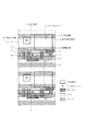
尚、図1において、1は光電変換領域としてのフォトダイオード、2は増幅トランジスタとしてのソースフォロア入力MOSトランジスタ、3は転送スイッチとしての転送MOSトランジスタ、4はリセットスイッチとしてのリセットMOSトランジスタ、5は選択スイッチとしての選択MOSトランジスタ、6は第一の配線層としての垂直信号線(垂直方向配線)、11は単位画素領域を表している。尚、本実施形態の単位画素領域11はフォトダイオード1、ソースフォロア入力MOSトランジスタ2、転送MOSトランジスタ及び選択MOSトランジスタを含んだ相補性金属酸化膜半導体(CMOS)を一例として用いているが、本発明は本画素構造に限定されない。12は第二の配線層としての駆動配線(水平方向配線)、13は第二の配線層としてのGND配線(水平方向配線)、14はトランジスタのソース・ドレイン領域、X−X’はつなぎ露光技術を用いて複数のパターンをつないだ際のつなぎ位置である。
【0019】
尚、第一の配線層及び第二の配線層は、それぞれが複数の配線層であっても良い。
【0020】
例えば、本実施形態においては第一配線層として駆動配線12及び
GND配線13が同一の配線層で形成されているが、別々の配線層で形成されていても良い。
【0021】
又、本図においてGNDとGND配線およびゲートと駆動配線の接続は省略されている。
【0022】
又、図1は2画素のみを示しているが、実際の固体撮像装置は、このような構造の画素が2次元状に多数隣接して配置されている。
【0023】
本実施形態においては、つなぎ位置を跨がない垂直信号線6は、例えば微細加工対応の縮小投影装置でつなぎ露光により形成し、つなぎ位置を跨ぐ領域を有する駆動配線12及びGND配線13は露光面積の大きい縮小投影装置を用いて一括露光により形成していることを特徴とする。
【0024】
すなわち、つなぎ位置を跨ぐ領域を有する第二の配線層は露光面積の大きい縮小投影装置を用いて一括露光することを特徴とする。
【0025】
又、つなぎ位置を跨がない第一の配線層は、つなぎ位置を跨ぐことがないため、微細加工対応の縮小投影装置で微細配線を形成することが可能である。すなわち、所望パターンを複数に分割し、分割されたパターンをつなぎ合わせて露光することでパターン形成を得る。
【0026】
従って、本実施形態の半導体装置の製造方法は、つなぎ位置を跨がない配線層を微細加工対応の縮小投影装置を用いてつなぎ露光で形成し、つなぎ位置を跨ぐ領域を有する配線層は露光面積の大きい縮小投影装置を用いて一括露光する。すなわち、つなぎ位置を跨ぐ領域を有する配線層はマージンを考慮に入れて微細加工対応の縮小投影露光装置を用いてつなぎ露光で配線層を形成する場合に比べて、工程数を各段に減らすことが可能となり、効率的に、感度の高い固体撮像装置を得ることが可能となる。
【0027】
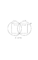
尚、例えば半導体装置としての固体撮像装置が、図1に示すような画素を複数有し、長辺を横方向、短辺を縦方向とした長方形を有する場合、縮小投影装置でのパターン形成におけるショット内の有効な領域のアスペクト比はおよそ縦:横=1:1であるために、効率の良いつなぎ露光としては、図2に示す水平方向に2分割あるいは図3に示す3分割する方法が考えられる。
【0028】
図2はチップ200をつなぎ位置201により、パターンL、パターンRに2分割し、それぞれをショットL、ショットRで露光するものである。
【0029】
図3はチップ300をつなぎ位置301、つなぎ位置302により、パターンL、パターンM、パターンRに3分割し、それぞれをショットL、ショットM、ショットRで露光するものである。
【0030】
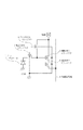
図4(A)は垂直方向配線であるmetal1をつなぎ露光によってパターン形成する様子を説明する図であり、1チップを図中分割位置によって2分割し、ショットL、ショットRによってつなぎ露光することにより所望パターンを形成する。図1の単位画素においてつなぎ位置401は、metal1を跨がないような位置に選ぶ。図4(B)はmetal2を一括露光によってパターン形成する様子を説明している。
【0031】
以上説明したように本発明の半導体装置及び固体撮像装置の製造方法によって、高開口率の確保、従って感度向上、或いは、適切な開口形状を得ることにより周辺画素の感度向上を図ることが可能となる。
【0032】
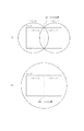
また、縮小投影装置のショット内では像高が大きくなるに従って解像度が低下する。例えば像高が大きくなると図4(A)のつなぎ位置401付近で解像度が低下する。すなわちつなぎ位置401付近においてパターンが存在する場合、解像度の低下によるパターン不良の発生が起こり得る。このようなパターン不良を避ける為に、図5(B)に示すように1チップをつなぎ位置501及び502によって3分割し、ショットL、ショットM、ショットRによってつなぎ露光することにより所望パターンを形成する方法も考えられる。これにより像高の低い、従って解像度の高いレンズ中央に近い部分での良好なパターン形成により半導体装置或いは固体撮像装置を形成することが可能である。
【0033】
尚、つなぎ位置の位置及びつなぎ回数は、チップの大きさ或いは露光装置の性能によって適宜決まり得るものであり、本実施形態の回数に限定されない。
【0034】
次に、図6は本発明の半導体装置及び固体撮像装置の製造方法で形成された固体撮像装置に搭載可能なCMOSセンサの単位画素の一例を示した回路図である。
【0035】
尚、既に前述した部分と同様の部分には同一符号を付している。
【0036】
具体的に説明するに、フォトダイオード1は転送MOSトランジスタ3を介してソースフォロア入力MOSトランジスタ2のゲートに接続され、ソースフォロア入力MOSトランジスタのソースは選択MOSトランジスタ5を介して垂直信号線6へと接続されている。また、ソースフォロア入力MOSトランジスタ2のゲートを所定電位にリセットするリセットMOSトランジスタ4が設けられている。また、駆動時の過渡的なGND電位の変動を抑制するために画素毎にGNDに接続されるGND配線が設けられている(本図では省略)。
【0037】
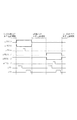
次に、本画素の動作を図7の等価回路図および図8のタイミングチャートを用いて説明する。図7において、単位画素は図6の等価回路図で示されるものである。また、図7において単位画素とGNDの接続は省略されている。垂直走査回路7によってある行(n行とする)が選択されたとき、まずリセット信号φRES(n)がローとなり、リセットスイッチがオフする。次に選択信号φSEL(n)がハイとなり、選択スイッチがオンとなりことで増幅MOSトランジスタのソースは垂直出力線と導通し、選択された画素と定電流負荷8によって、ソースフォロア回路が形成される。つづいてφTNがハイとなり、転送ゲートを介して画素のリセット状態に対応するN出力がラインメモリ9に読み出される。その後、転送パルスφTX(n)によって転送スイッチが一定期間オンとなり、光電変換素子で発生した光信号が増幅MOSトランジスタのゲートに転送される。ひきつづきφTSがハイとなり、光信号に対応したS出力がラインメモリに読み出される。次に、逐次、水平走査回路によって選択された列のN信号、S信号が読み出され、これら相関のあるN信号とS信号の差分を実行することにより、光応答出力が得られる。
【0038】
このように、選択された行の画素の信号を同時にラインメモリに転送した後に逐次読み出すため、画素の駆動を行う選択MOSトランジスタ、転送MOSトランジスタ、リセットMOSトランジスタの制御線はつなぎ位置を跨ぐ水平方向の配線により構成され、つなぎ位置を跨がない信号線は垂直方向の配線で構成される。尚、本実施形態においては、GND線はつなぎ位置を跨ぐ領域を有する水平方向で形成されている。
【0039】
(実施形態2)
図9は本発明の半導体装置の製造方法を用いて形成された半導体装置の上面図である。尚、本実施形態においては第一実施形態と同様に半導体装置の一例として、光を信号電荷に変換する光電変換領域を有する固体撮像装置を例にあげて説明するが、本発明は固体撮像装置に限定されず、複数の配線層を有する半導体装置であれば良い。
【0040】
20は第一の配線層としてつなぎ位置を跨がない配線層としてのGND配線である。
【0041】
尚、既に前述した部分と同様の部分には同一符号を付している。
【0042】
図9で示される単位画素は高開口率を確保するため、つなぎ位置を跨ぐ領域を有する第二の配線層として駆動配線12、つなぎ位置を跨がない第一の配線層線としてGND配線20及び垂直出力線6を垂直方向配線としている。本例では、第二の配線層としての水平方向配線はmetal2で構成され、第一の配線層はmetal1で構成されている。
【0043】
本実施形態は図6で示される単位画素のGND線を垂直方向配線で構成した場合のレイアウト図の一例であり、本図においてゲートと駆動配線の接続は省略されている。
【0044】
また、図9は2画素のみを示しているが、実際の固体撮像装置は、このような構造の画素が2次元状に多数隣接して配置されている。
【0045】
本実施形態が第一実施形態と異なる点は、第一実施形態ではGND配線13はつなぎ位置を跨ぐ領域を有する様に一括露光で配置していたのに対し、本実施形態ではGND配線20はつなぎ位置を跨がない様につなぎ露光技術を用いて形成されている点である。
【0046】
具体的に説明するに、前述したようにつなぎ位置を跨ぐ領域を有する配線層は、つなぎ露光技術を用いてもマージンを考慮する必要があるので一括露光に比べて配線幅、配線間スペースで有利になり得ない。すなわち、つなぎ位置を跨ぐ領域を有する第二の配線層は一括露光、つなぎ露光いずれの方法を用いた場合でも配線幅、配線間スペースに関して微細加工を行うことができず、開口率の低下、感度の低下、或いは開口形状の偏り、周辺画素の感度低下、また更には、分割位置の左右のショットのアライメントズレに起因する感度ズレがあった。従って、つなぎ位置を跨ぐ領域を有する第二の配線層は少ない程良い。
【0047】
さらに具体的に説明するに、図10(A)は実施形態1の図1に示す固体撮像装置が例えば画素数300万画素の固体撮像装置の中央付近に配置された中央画素の際の線10−10’における模式的断面図、図10(B)は実施形態1の図1に示す固体撮像装置が例えば画素数300万画素の端部付近に配置された周辺画素の際の線10−10’における模式的断面図、図11(A)は本実施形態の図9に示す固体撮像装置が例えば画素数300万画素の固体撮像装置の中央付近に配置された中央画素の際の線11−11における模式的断面、図10(B)は本実施形態の図9に示す固体撮像装置が例えば画素数300万画素の端部付近に配置された周辺画素の際の線11−11’における模式的断面図である。
【0048】
図10(A)及び図10(B)においてmetal2の配線層は、選択MOSトランジスタ5、転送MOSトランジスタ3、リセットMOSトランジスタ4の駆動配線12及びGND配線層13を有する配線層である。また、metal2は遮光層兼電源を兼ねている。図10(A)で示される中央画素は、metal2の配線層であるGND配線層13と転送MOSトランジスタ3の駆動配線12とによって光路が決定されている。しかしながら図10(B)に示すように、周辺画素では中央画素に比べて斜め方向から入射する光が多いため中央画素(図10(A))と比較して光路が遮られる量が多く、従って周辺画素では中央画素よりも感度が低くなる。さらに、metal2の配線層によって開口部が規定されているため、つなぎ位置の左右のショットのアライメントズレの違いによってつなぎ位置の左右で感度が異なるという問題も起こり得る。
【0049】
一方、図11(A)及び図11(B)ではGND配線13が無いため、光路は転送MOSトランジスタ3と選択MOSトランジスタ5の駆動配線で開口部が規定される。従って、周辺画素(図11(B))において光が斜めから入射しても開口部が広いため光路が遮られ難い。従って、中央画素と周辺画素との感度のバラツキが低減された固体撮像装置が提供できる。さらには、つなぎ露光技術を用いて半導体装置及び固体撮像装置を製造した場合、つなぎ位置の左右のショットにおけるアライメントズレに起因する感度ズレが防げる。
【0050】
尚、実施形態1及び本実施形態において、第二の配線層をmetal1で構成し、第一の配線層をmetal2で構成しても良い。この場合、metal2をつなぎ露光によりパターン形成し、metal1を一括露光によりパターン形成することにより、本発明の効果が得られる。
【0051】
また、本発明は、単位画素の等価回路図が図4に示される例に限らず、つなぎ露光、一括露光の両者を用いてパターン形成を行う半導体装置及び固体撮像装置について適用可能なものである。例えば、図12の等価回路図で示される単位画素を行列状に配置して成る固体撮像装置においても同様の効果が得られる。図12と図4は、図4においては選択MOSトランジスタ5がソースフォロア入力MOSトランジスタ2に対して垂直出力線6側に接続されるのに対して、図12においては選択MOSトランジスタ5がソースフォロア入力MOSトランジスタ2に対して電源側に接続される点で異なる。尚、動作タイミングは両者同様である。
【0052】
【発明の効果】
以上述べたように、複数の配線層を有する半導体装置或いは固体撮像装置の製造方法において、つなぎ位置を跨ぐ領域を有する配線層を一括露光によりパターン形成し、つなぎ位置を跨がない配線層をつなぎ露光パターン形成することで工程数を各段に減らすことが可能となり、効率的に、感度の高い半導体装置或いは固体撮像装置を得ることが可能となった。
【0053】
又、画素部の構成に関して、画素の駆動線を水平方向配線とし、駆動線以外の配線を垂直方向配線とすることにより、有効な微細化による高開口率の確保、従って感度向上、或いは、適切な開口形状を得ることによる周辺画素の感度向上、及び、つなぎ位置での感度ズレのない良好な画質を実現することが可能となる。
【図面の簡単な説明】
【図1】本発明の固体撮像装置の製造方法を用いて形成された固体撮像装置の実施形態1の単位画素の上面図である。
【図2】実施形態1におけるつなぎ露光を説明するための上面図である。
【図3】実施形態1におけるつなぎ露光を説明するための上面図である。
【図4】本発明の半導体装置の製造方法を説明した図である。
【図5】本発明の半導体装置の製造方法を説明した図である。
【図6】実施形態1のCMOSセンサの単位画素の等価回路図である。
【図7】実施形態1のCMOSセンサの動作を説明する等価回路図である。
【図8】実施形態1のCMOSセンサの動作を説明するタイミング図である。
【図9】本発明の固体撮像装置の製造方法を用いて形成された固体撮像装置の実施形態2の単位画素の上面図である。
【図10】図1における線8−8’における模式的断面図である。
【図11】図9における線9−9’における模式的断面図である。
【図12】本発明の固体撮像装置の製造方法で形成された固体撮像装置の等価回路図である。
【図13】従来技術の半導体装置の製造方法を説明するための模式的パターン図である。
【図14】従来技術において、つなぎ露光を用いた際のつなぎ位置での配線形状を説明する図である。
【符号の説明】
1 フォトダイオード
2 ソースフォロア入力MOSトランジスタ
3 転送MOSトランジスタ
4 リセットMOSトランジスタ
5 選択MOSトランジスタ
6 垂直信号線
7 垂直走査回路
8 定電流源
9 ラインメモリ
10 水平走査回路
11 単位画素領域
12 駆動配線
13 GND配線[0001]
TECHNICAL FIELD OF THE INVENTION
The present invention relates to a method for manufacturing a semiconductor device and a solid-state imaging device, and more particularly to a method for manufacturing a semiconductor device and a solid-state imaging device using a bridge exposure in which a desired pattern is divided into a plurality of patterns and the divided patterns are connected and exposed.
[0002]
[Prior art]
When a semiconductor device having a large chip size is formed on a semiconductor substrate, for example, a method of manufacturing a semiconductor device described in Japanese Patent Application Laid-Open No. 5-6849 is known.
[0003]
[Patent Document 1]
JP-A-5-6849
FIGS. 13A to 13C show a method of manufacturing a semiconductor device described in JP-A-5-6849.
[0005]
FIG. 13A is a schematic pattern diagram of a first layer on a semiconductor substrate for explaining a conventional method of manufacturing a semiconductor device, and FIG. 13B is for forming the first layer of FIG. FIG. 13C is a schematic pattern diagram of a second reticle for forming a second layer.
[0006]
In the first reticle 105, patterns A, B, and C are provided divided into three, and an IC pattern is formed in each of the patterns. Patterns A, B, and C are arranged vertically, connected, and the connected patterns A, B, and C constitute one chip.
[0007]
The first reticle 105 is set in a reduction projection type exposure apparatus, and a pattern attached to a semiconductor substrate 101 (hereinafter, referred to as a wafer 101) is connected to a semiconductor substrate 101 (hereinafter, referred to as a wafer 101) by a system attached to the apparatus. The layout of the first layer on the wafer 101 is programmed so that is printed. The
[0008]
When printing the first layer, the first reticle 105 changes the position of the masking blade of the reduction projection type exposure apparatus for each shot (patterns A, B, and C) to print the pattern A portion. The portions of the patterns B and C are hidden by this blade so that light does not pass therethrough. The same applies when printing patterns B and C, respectively.
[0009]
After the patterns A, B, and C are formed, a normal semiconductor manufacturing process such as etching, impurity diffusion, or deposition of a CVD (Chemical Vapor Deposition) film or the like is performed by the patterns, and then a pattern in the second layer is formed.
[0010]
Next, in the second layer, alignment is performed using the
[0011]
Further, in the related art, a wiring that straddles a connecting position is formed by using a connecting exposure technique that divides a desired pattern into a plurality of parts by using a reduction processing device compatible with microfabrication, and connects and exposes the divided patterns. In this case, as shown in FIG. 14, the wiring straddling the connection position has a margin in consideration of the alignment accuracy of the left and right shots with respect to the connection position.
[0012]
[Problems to be solved by the invention]
However, in a semiconductor device and a solid-state imaging device having a plurality of wiring layers in which a wiring layer having a region that straddles a connecting position and a wiring layer having no straddling position, a wiring layer having a region that straddles a connecting position is divided. As described above, when the patterns are connected, the patterns are formed in consideration of the alignment margin. Therefore, the number of processes is increased, and the reduced projection area having a large exposure area is used despite the use of the reduced projection apparatus capable of fine processing. There is no advantage in the wiring width and the space between the wirings as compared with the case of forming by batch exposure using an apparatus.
[0013]
[Means for Solving the Problems]
The present invention has been made in view of the above problems, and an object of the present invention is to provide a method of manufacturing a semiconductor device using bridge exposure, which reduces the number of steps and efficiently manufactures a semiconductor device with high sensitivity. It is in.
[0014]
In order to solve the above problem, a method of manufacturing a semiconductor device according to the present invention is a method of manufacturing a semiconductor device having a plurality of wiring layers, wherein the first wiring layer divides a desired pattern into a plurality of patterns, and A pattern is formed by connecting and exposing, and the second wiring layer is pattern-formed by batch exposure.
[0015]
It is another object of the present invention to provide a method of manufacturing a solid-state imaging device using bridge exposure, in which the number of steps is reduced and a semiconductor device with high sensitivity is efficiently manufactured.
[0016]
In order to solve the above-described problems, the solid-state imaging device of the present invention includes a pixel having a photoelectric conversion region that converts light into a signal charge, a plurality of wiring layers including a first wiring layer and a second wiring layer, In the method for manufacturing a solid-state imaging device having, the first wiring layer is formed by dividing a desired pattern into a plurality of patterns, connecting the divided patterns and exposing the patterns, and forming the second wiring layer by batch exposure. It is characterized by being patterned.
[0017]
BEST MODE FOR CARRYING OUT THE INVENTION
(Embodiment 1)
FIG. 1 is a top view of a semiconductor device formed by using the semiconductor device manufacturing method of the present invention. In the present embodiment, a solid-state imaging device having a photoelectric conversion region that converts light into signal charges will be described as an example of a semiconductor device. However, the present invention is not limited to a solid-state imaging device. Any semiconductor device having a wiring layer may be used.
[0018]
In FIG. 1, 1 is a photodiode as a photoelectric conversion region, 2 is a source follower input MOS transistor as an amplifying transistor, 3 is a transfer MOS transistor as a transfer switch, 4 is a reset MOS transistor as a reset switch, and 5 is a reset MOS transistor. A selection MOS transistor as a selection switch, 6 is a vertical signal line (vertical wiring) as a first wiring layer, and 11 is a unit pixel region. The
[0019]
Note that each of the first wiring layer and the second wiring layer may be a plurality of wiring layers.
[0020]
For example, in the present embodiment, the
[0021]
In this figure, connection between GND and GND wiring and connection between gate and driving wiring are omitted.
[0022]
Although FIG. 1 shows only two pixels, in an actual solid-state imaging device, many pixels having such a structure are arranged adjacent to each other in a two-dimensional manner.
[0023]
In the present embodiment, the vertical signal line 6 that does not extend over the connection position is formed by, for example, connection exposure using a reduction projection device compatible with fine processing, and the
[0024]
That is, the second wiring layer having a region straddling the connection position is collectively exposed using a reduction projection device having a large exposure area.
[0025]
Further, since the first wiring layer which does not straddle the connecting position does not straddle the connecting position, it is possible to form a fine wiring by a reduction projection apparatus compatible with fine processing. In other words, the desired pattern is divided into a plurality of patterns, and the divided patterns are joined together and exposed to obtain a pattern.
[0026]
Therefore, in the method of manufacturing a semiconductor device according to the present embodiment, a wiring layer that does not straddle a joint position is formed by joint exposure using a reduction projection device compatible with fine processing, and a wiring layer having a region that straddles the joint position has an exposure area Exposure is performed using a reduction projection apparatus having a large size. In other words, the number of steps is reduced to each step as compared with the case where a wiring layer having a region straddling a connecting position is formed by connecting and exposing the wiring layer using a reduced projection exposure apparatus compatible with fine processing in consideration of a margin. This makes it possible to efficiently obtain a solid-state imaging device with high sensitivity.
[0027]
Note that, for example, when a solid-state imaging device as a semiconductor device has a plurality of pixels as shown in FIG. 1 and has a rectangular shape having a long side in a horizontal direction and a short side in a vertical direction, when a pattern is formed by a reduction projection device. Since the effective area in the shot has an aspect ratio of about vertical: horizontal = 1: 1, efficient split exposure is performed by dividing horizontally into two as shown in FIG. 2 or into three as shown in FIG. Conceivable.
[0028]
FIG. 2 shows that a
[0029]
FIG. 3 shows that the
[0030]
FIG. 4A is a view for explaining how a pattern is formed by connecting and exposing
[0031]
As described above, the method for manufacturing a semiconductor device and a solid-state imaging device according to the present invention makes it possible to secure a high aperture ratio and thus improve the sensitivity, or to improve the sensitivity of peripheral pixels by obtaining an appropriate aperture shape. Become.
[0032]
Also, within a shot of the reduction projection device, the resolution decreases as the image height increases. For example, when the image height increases, the resolution decreases near the connection position 401 in FIG. That is, when a pattern exists near the connection position 401, a pattern defect may occur due to a reduction in resolution. In order to avoid such a pattern defect, as shown in FIG. 5B, one chip is divided into three parts by connecting positions 501 and 502, and a desired pattern is formed by connecting and exposing shots L, M and R. There is also a way to do this. This makes it possible to form a semiconductor device or a solid-state imaging device by forming a good pattern in a portion near the center of the lens where the image height is low and thus the resolution is high.
[0033]
The position of the connection position and the number of connections can be appropriately determined depending on the size of the chip or the performance of the exposure apparatus, and are not limited to the number of times in the present embodiment.
[0034]
Next, FIG. 6 is a circuit diagram showing an example of a unit pixel of a CMOS sensor that can be mounted on a solid-state imaging device formed by the method of manufacturing a semiconductor device and a solid-state imaging device of the present invention.
[0035]
The same parts as those already described are denoted by the same reference numerals.
[0036]
More specifically, the
[0037]
Next, the operation of the present pixel will be described with reference to an equivalent circuit diagram of FIG. 7 and a timing chart of FIG. In FIG. 7, the unit pixel is shown in the equivalent circuit diagram of FIG. In FIG. 7, the connection between the unit pixel and GND is omitted. When a certain row (n-th row) is selected by the vertical scanning circuit 7, first, the reset signal φRES (n) becomes low, and the reset switch is turned off. Next, the selection signal φSEL (n) becomes high and the selection switch is turned on, so that the source of the amplifying MOS transistor conducts with the vertical output line, and a source follower circuit is formed by the selected pixel and the constant
[0038]
As described above, since the signals of the pixels in the selected row are simultaneously transferred to the line memory and sequentially read out, the control lines of the selection MOS transistor, the transfer MOS transistor, and the reset MOS transistor for driving the pixels are connected in the horizontal direction across the connection position. The signal line which does not straddle the connecting position is formed by a vertical wiring. In the present embodiment, the GND lines are formed in a horizontal direction having a region extending over the connection position.
[0039]
(Embodiment 2)
FIG. 9 is a top view of a semiconductor device formed by using the semiconductor device manufacturing method of the present invention. In the present embodiment, as in the first embodiment, a solid-state imaging device having a photoelectric conversion region that converts light into signal charges will be described as an example of a semiconductor device. The present invention is not limited to this, and may be any semiconductor device having a plurality of wiring layers.
[0040]
[0041]
The same parts as those already described are denoted by the same reference numerals.
[0042]
In order to secure a high aperture ratio, the unit pixel shown in FIG. 9 has a
[0043]
This embodiment is an example of a layout diagram in the case where the GND line of the unit pixel shown in FIG. 6 is formed by vertical wiring, and the connection between the gate and the driving wiring is omitted in this drawing.
[0044]
FIG. 9 shows only two pixels, but in an actual solid-state imaging device, many pixels having such a structure are arranged adjacent to each other in a two-dimensional shape.
[0045]
The difference of the present embodiment from the first embodiment is that, in the first embodiment, the
[0046]
More specifically, as described above, a wiring layer having a region that straddles a connecting position requires a margin even when using a connecting exposure technique, and thus has an advantage in wiring width and space between wirings compared to batch exposure. Can not be. That is, the second wiring layer having a region straddling the connection position cannot perform fine processing with respect to the wiring width and the space between the wirings using either the batch exposure method or the connection exposure method, resulting in a decrease in aperture ratio and sensitivity. Or the deviation of the aperture shape, the sensitivity of the peripheral pixels is reduced, and further, the sensitivity shift due to the alignment shift between the left and right shots at the division position. Therefore, it is better that the number of the second wiring layers having a region extending over the connecting position is smaller.
[0047]
More specifically, FIG. 10A illustrates a
[0048]
10A and 10B, the wiring layer of metal2 is a wiring layer having the driving
[0049]
On the other hand, in FIGS. 11A and 11B, since there is no
[0050]
In the first embodiment and the present embodiment, the second wiring layer may be formed of metal1, and the first wiring layer may be formed of metal2. In this case, the effect of the present invention can be obtained by forming a pattern on metal2 by connecting exposure and forming a pattern on metal1 by batch exposure.
[0051]
Further, the present invention is applicable not only to the example in which the equivalent circuit diagram of the unit pixel is shown in FIG. 4, but also to a semiconductor device and a solid-state imaging device which form a pattern using both the link exposure and the batch exposure. . For example, the same effect can be obtained in a solid-state imaging device in which the unit pixels shown in the equivalent circuit diagram of FIG. 12 are arranged in a matrix. 12 and FIG. 4 show that the
[0052]
【The invention's effect】
As described above, in a method of manufacturing a semiconductor device or a solid-state imaging device having a plurality of wiring layers, a wiring layer having a region that straddles a connecting position is pattern-formed by batch exposure, and a wiring layer that does not straddle a connecting position is connected. By forming an exposure pattern, the number of steps can be reduced to each step, and a semiconductor device or a solid-state imaging device with high sensitivity can be efficiently obtained.
[0053]
Further, regarding the configuration of the pixel portion, by setting the driving lines of the pixels to horizontal wirings and the wirings other than the driving lines to vertical wirings, it is possible to secure a high aperture ratio by effective miniaturization, and thus to improve the sensitivity or improve the sensitivity. It is possible to improve the sensitivity of the peripheral pixels by obtaining a proper aperture shape, and to realize a good image quality without a sensitivity shift at the joint position.
[Brief description of the drawings]
FIG. 1 is a top view of a unit pixel according to a first embodiment of a solid-state imaging device formed using a method for manufacturing a solid-state imaging device of the present invention.
FIG. 2 is a top view for explaining connection exposure in the first embodiment.
FIG. 3 is a top view for explaining connection exposure in the first embodiment.
FIG. 4 is a diagram illustrating a method for manufacturing a semiconductor device according to the present invention.
FIG. 5 is a diagram illustrating a method for manufacturing a semiconductor device according to the present invention.
FIG. 6 is an equivalent circuit diagram of a unit pixel of the CMOS sensor according to the first embodiment.
FIG. 7 is an equivalent circuit diagram for explaining the operation of the CMOS sensor according to the first embodiment.
FIG. 8 is a timing chart for explaining the operation of the CMOS sensor according to the first embodiment;
FIG. 9 is a top view of a unit pixel according to a second embodiment of the solid-state imaging device formed by using the method for manufacturing a solid-state imaging device of the present invention.
FIG. 10 is a schematic sectional view taken along line 8-8 ′ in FIG. 1;
11 is a schematic sectional view taken along line 9-9 'in FIG.
FIG. 12 is an equivalent circuit diagram of a solid-state imaging device formed by the method for manufacturing a solid-state imaging device of the present invention.
FIG. 13 is a schematic pattern diagram for explaining a conventional method of manufacturing a semiconductor device.
FIG. 14 is a diagram illustrating a wiring shape at a connection position when connection exposure is used in the conventional technique.
[Explanation of symbols]
REFERENCE SIGNS
Claims (8)
第一の配線層は所望パターンを複数に分割し、前記分割されたパターンをつなぎ合わせて露光することでパターン形成され、
第二の配線層は一括露光によりパターン形成されることを特徴とする半導体装置の製造方法。In a method for manufacturing a semiconductor device having a plurality of wiring layers,
The first wiring layer is formed by dividing a desired pattern into a plurality of patterns, and connecting and exposing the divided patterns to form a pattern.
A method for manufacturing a semiconductor device, wherein a pattern of a second wiring layer is formed by batch exposure.
第一の配線層は所望パターンを複数に分割し、前記分割されたパターンをつなぎ合わせて露光することでパターン形成され、
第二の配線層は一括露光によりパターン形成されることを特徴とする固体撮像装置の製造方法。A pixel having a photoelectric conversion region for converting light into signal charges, and a plurality of wiring layers including a first wiring layer and a second wiring layer, in a method for manufacturing a solid-state imaging device having:
The first wiring layer is formed by dividing a desired pattern into a plurality of patterns, and connecting and exposing the divided patterns to form a pattern.
A method for manufacturing a solid-state imaging device, wherein a pattern of a second wiring layer is formed by batch exposure.
Priority Applications (9)
| Application Number | Priority Date | Filing Date | Title |
|---|---|---|---|
| JP2002275019A JP4109944B2 (en) | 2002-09-20 | 2002-09-20 | Method for manufacturing solid-state imaging device |
| TW092125506A TWI228824B (en) | 2002-09-20 | 2003-09-16 | Manufacturing methods of semiconductor device and solid state image pickup device |
| KR10-2003-0064885A KR100533400B1 (en) | 2002-09-20 | 2003-09-18 | Manufacturing methods of semiconductor device and solid state image pickup device |
| EP03021244A EP1401023B1 (en) | 2002-09-20 | 2003-09-18 | Manufacturing methods of semiconductor device and solid state image pickup device |
| DE60322808T DE60322808D1 (en) | 2002-09-20 | 2003-09-18 | A method of manufacturing a semiconductor device and a solid state image pickup device |
| CNB03158585XA CN1252800C (en) | 2002-09-20 | 2003-09-19 | Method for mfg. semiconductor and solid photographic device |
| US10/665,593 US7087983B2 (en) | 2002-09-20 | 2003-09-22 | Manufacturing methods of semiconductor devices and a solid state image pickup device |
| US11/132,242 US7838957B2 (en) | 2002-09-20 | 2005-05-19 | Semiconductor device having a plurality of photoelectric conversion elements, a transfer transistor, an amplifying transistor, a reset transistor, and a plurality of wirings defining an aperture of the photoelectric conversion elements |
| US12/911,844 US8183084B2 (en) | 2002-09-20 | 2010-10-26 | Methods of manufacturing solid state image pickup devices |
Applications Claiming Priority (1)
| Application Number | Priority Date | Filing Date | Title |
|---|---|---|---|
| JP2002275019A JP4109944B2 (en) | 2002-09-20 | 2002-09-20 | Method for manufacturing solid-state imaging device |
Publications (2)
| Publication Number | Publication Date |
|---|---|
| JP2004111802A true JP2004111802A (en) | 2004-04-08 |
| JP4109944B2 JP4109944B2 (en) | 2008-07-02 |
Family
ID=31944600
Family Applications (1)
| Application Number | Title | Priority Date | Filing Date |
|---|---|---|---|
| JP2002275019A Expired - Fee Related JP4109944B2 (en) | 2002-09-20 | 2002-09-20 | Method for manufacturing solid-state imaging device |
Country Status (7)
| Country | Link |
|---|---|
| US (3) | US7087983B2 (en) |
| EP (1) | EP1401023B1 (en) |
| JP (1) | JP4109944B2 (en) |
| KR (1) | KR100533400B1 (en) |
| CN (1) | CN1252800C (en) |
| DE (1) | DE60322808D1 (en) |
| TW (1) | TWI228824B (en) |
Cited By (9)
| Publication number | Priority date | Publication date | Assignee | Title |
|---|---|---|---|---|
| JP2006073624A (en) * | 2004-08-31 | 2006-03-16 | Canon Inc | Method for manufacturing semiconductor device |
| JP2006203032A (en) * | 2005-01-21 | 2006-08-03 | Victor Co Of Japan Ltd | Method of manufacturing element |
| JP2006337857A (en) * | 2005-06-03 | 2006-12-14 | Toshiba Microelectronics Corp | Semiconductor device manufacturing method and semiconductor device chip pattern correction program |
| JP2013033870A (en) * | 2011-08-02 | 2013-02-14 | Canon Inc | Semiconductor device and manufacturing method thereof |
| JP2013145900A (en) * | 2013-02-27 | 2013-07-25 | Renesas Electronics Corp | Method of manufacturing solid-state imaging element, and solid-state imaging element |
| JP2013182943A (en) * | 2012-02-29 | 2013-09-12 | Canon Inc | Method of manufacturing solid state imaging device |
| JP2014112740A (en) * | 2014-03-24 | 2014-06-19 | Renesas Electronics Corp | Method of manufacturing solid-state imaging element, and solid-state imaging element |
| JP2017183658A (en) * | 2016-03-31 | 2017-10-05 | ソニー株式会社 | Solid-state imaging device, imaging device, and electronic device |
| US12138928B2 (en) | 2021-08-13 | 2024-11-12 | Canon Kabushiki Kaisha | Method for manufacturing liquid ejection head substrate and method for manufacturing liquid ejection head |
Families Citing this family (9)
| Publication number | Priority date | Publication date | Assignee | Title |
|---|---|---|---|---|
| US7851837B2 (en) * | 2003-12-18 | 2010-12-14 | Panasonic Corporation | Light-collecting device and solid-state imaging apparatus |
| JP3890333B2 (en) * | 2004-02-06 | 2007-03-07 | キヤノン株式会社 | Solid-state imaging device |
| JP4508891B2 (en) * | 2005-01-28 | 2010-07-21 | キヤノン株式会社 | PHOTOELECTRIC CONVERSION DEVICE, MULTI-CHIP IMAGE SENSOR, TOUCH TYPE IMAGE SENSOR AND IMAGE READING DEVICE |
| KR20070093335A (en) * | 2006-03-13 | 2007-09-18 | 마쯔시다덴기산교 가부시키가이샤 | Solid state imaging device and driving method thereof |
| KR100881200B1 (en) * | 2007-07-30 | 2009-02-05 | 삼성전자주식회사 | CMOS image sensor and its manufacturing method |
| US8035716B2 (en) * | 2008-06-13 | 2011-10-11 | Omnivision Technologies, Inc. | Wide aperture image sensor pixel |
| WO2012119098A2 (en) * | 2011-03-02 | 2012-09-07 | Texas Instruments Incorporated | Pattern-split decomposition strategy for double-patterned lithography process |
| KR102171022B1 (en) * | 2014-05-14 | 2020-10-28 | 삼성전자주식회사 | Image sensor for improving interference influence between pixels |
| US9741669B2 (en) | 2016-01-26 | 2017-08-22 | Taiwan Semiconductor Manufacturing Company, Ltd. | Forming large chips through stitching |
Family Cites Families (22)
| Publication number | Priority date | Publication date | Assignee | Title |
|---|---|---|---|---|
| JPS5710926A (en) * | 1980-06-25 | 1982-01-20 | Toshiba Corp | Manufacture of semiconductor device |
| EP0440470B1 (en) * | 1990-02-02 | 1996-12-18 | Canon Kabushiki Kaisha | Exposure method |
| US5561317A (en) * | 1990-08-24 | 1996-10-01 | Canon Kabushiki Kaisha | Method of manufacturing semiconductor devices |
| JP2902506B2 (en) * | 1990-08-24 | 1999-06-07 | キヤノン株式会社 | Semiconductor device manufacturing method and semiconductor device |
| JPH04326507A (en) | 1991-04-25 | 1992-11-16 | Canon Inc | Semiconductor alignment method |
| JPH05127186A (en) | 1991-11-01 | 1993-05-25 | Canon Inc | Formation of electrode pattern for liquid crystal-display element |
| JPH05136020A (en) * | 1991-11-11 | 1993-06-01 | Fujitsu Ltd | Exposure method of semiconductor device |
| JPH08262583A (en) * | 1995-03-28 | 1996-10-11 | Fuji Photo Film Co Ltd | Exposing method for divided image |
| JP3183390B2 (en) * | 1995-09-05 | 2001-07-09 | キヤノン株式会社 | Photoelectric conversion device and imaging device using the same |
| KR100468234B1 (en) * | 1996-05-08 | 2005-06-22 | 가부시키가이샤 니콘 | Exposure method, exposure apparatus and disc |
| JP3085259B2 (en) * | 1997-09-17 | 2000-09-04 | 日本電気株式会社 | Exposure pattern and method for generating the same |
| US6369853B1 (en) * | 1997-11-13 | 2002-04-09 | Foveon, Inc. | Intra-pixel frame storage element, array, and electronic shutter method suitable for electronic still camera applications |
| US6977684B1 (en) * | 1998-04-30 | 2005-12-20 | Canon Kabushiki Kaisha | Arrangement of circuits in pixels, each circuit shared by a plurality of pixels, in image sensing apparatus |
| US6192290B1 (en) * | 1998-05-21 | 2001-02-20 | Lucent Technologies Inc. | System and method of manufacturing semicustom integrated circuits using reticle primitives from a library and interconnect reticles |
| JP3819711B2 (en) * | 1998-10-23 | 2006-09-13 | 株式会社ルネサステクノロジ | Manufacturing method of semiconductor device |
| US6073343A (en) * | 1998-12-22 | 2000-06-13 | General Electric Company | Method of providing a variable guard ring width between detectors on a substrate |
| US6833234B1 (en) * | 2000-08-04 | 2004-12-21 | Massachusetts Institute Of Technology | Stereolithographic patterning with variable size exposure areas |
| JP4507392B2 (en) * | 2000-11-15 | 2010-07-21 | 株式会社ニコン | Electronic camera |
| US6580106B2 (en) * | 2001-01-12 | 2003-06-17 | Isetex. Inc | CMOS image sensor with complete pixel reset without kTC noise generation |
| JP5144863B2 (en) * | 2001-06-29 | 2013-02-13 | 株式会社オーク製作所 | Multiple exposure drawing method and multiple exposure drawing apparatus |
| JP3940310B2 (en) * | 2002-04-04 | 2007-07-04 | 株式会社日立ハイテクノロジーズ | Electron beam drawing method, drawing apparatus, and semiconductor manufacturing method using the same |
| JP4326507B2 (en) | 2005-07-11 | 2009-09-09 | 株式会社トプコン | Lens peripheral processing equipment |
-
2002
- 2002-09-20 JP JP2002275019A patent/JP4109944B2/en not_active Expired - Fee Related
-
2003
- 2003-09-16 TW TW092125506A patent/TWI228824B/en not_active IP Right Cessation
- 2003-09-18 EP EP03021244A patent/EP1401023B1/en not_active Expired - Lifetime
- 2003-09-18 KR KR10-2003-0064885A patent/KR100533400B1/en not_active IP Right Cessation
- 2003-09-18 DE DE60322808T patent/DE60322808D1/en not_active Expired - Lifetime
- 2003-09-19 CN CNB03158585XA patent/CN1252800C/en not_active Expired - Fee Related
- 2003-09-22 US US10/665,593 patent/US7087983B2/en not_active Expired - Fee Related
-
2005
- 2005-05-19 US US11/132,242 patent/US7838957B2/en not_active Expired - Fee Related
-
2010
- 2010-10-26 US US12/911,844 patent/US8183084B2/en not_active Expired - Fee Related
Cited By (13)
| Publication number | Priority date | Publication date | Assignee | Title |
|---|---|---|---|---|
| JP2006073624A (en) * | 2004-08-31 | 2006-03-16 | Canon Inc | Method for manufacturing semiconductor device |
| US7749691B2 (en) | 2004-08-31 | 2010-07-06 | Canon Kabushiki Kaisha | Method of manufacturing a photoelectric conversion device using a plurality of reticles |
| JP4646575B2 (en) * | 2004-08-31 | 2011-03-09 | キヤノン株式会社 | Manufacturing method of semiconductor device |
| US8105765B2 (en) | 2004-08-31 | 2012-01-31 | Canon Kabushiki Kaisha | Method of manufacturing a semiconductor device |
| JP2006203032A (en) * | 2005-01-21 | 2006-08-03 | Victor Co Of Japan Ltd | Method of manufacturing element |
| JP2006337857A (en) * | 2005-06-03 | 2006-12-14 | Toshiba Microelectronics Corp | Semiconductor device manufacturing method and semiconductor device chip pattern correction program |
| JP2013033870A (en) * | 2011-08-02 | 2013-02-14 | Canon Inc | Semiconductor device and manufacturing method thereof |
| JP2013182943A (en) * | 2012-02-29 | 2013-09-12 | Canon Inc | Method of manufacturing solid state imaging device |
| JP2013145900A (en) * | 2013-02-27 | 2013-07-25 | Renesas Electronics Corp | Method of manufacturing solid-state imaging element, and solid-state imaging element |
| JP2014112740A (en) * | 2014-03-24 | 2014-06-19 | Renesas Electronics Corp | Method of manufacturing solid-state imaging element, and solid-state imaging element |
| JP2017183658A (en) * | 2016-03-31 | 2017-10-05 | ソニー株式会社 | Solid-state imaging device, imaging device, and electronic device |
| US10798318B2 (en) | 2016-03-31 | 2020-10-06 | Sony Corporation | Solid-state imaging element, imaging device, and electronic device |
| US12138928B2 (en) | 2021-08-13 | 2024-11-12 | Canon Kabushiki Kaisha | Method for manufacturing liquid ejection head substrate and method for manufacturing liquid ejection head |
Also Published As
| Publication number | Publication date |
|---|---|
| CN1252800C (en) | 2006-04-19 |
| US20110045632A1 (en) | 2011-02-24 |
| KR100533400B1 (en) | 2005-12-02 |
| TW200414526A (en) | 2004-08-01 |
| KR20040025836A (en) | 2004-03-26 |
| US7838957B2 (en) | 2010-11-23 |
| US20050212096A1 (en) | 2005-09-29 |
| US20040126934A1 (en) | 2004-07-01 |
| EP1401023B1 (en) | 2008-08-13 |
| DE60322808D1 (en) | 2008-09-25 |
| EP1401023A3 (en) | 2006-03-15 |
| US8183084B2 (en) | 2012-05-22 |
| EP1401023A2 (en) | 2004-03-24 |
| US7087983B2 (en) | 2006-08-08 |
| CN1495855A (en) | 2004-05-12 |
| TWI228824B (en) | 2005-03-01 |
| JP4109944B2 (en) | 2008-07-02 |
Similar Documents
| Publication | Publication Date | Title |
|---|---|---|
| JP4109944B2 (en) | Method for manufacturing solid-state imaging device | |
| JP4832660B2 (en) | Image sensing element and manufacturing method thereof | |
| KR101683297B1 (en) | Solid-state imaging device, solid-state imaging device manufacturing method, elelctronic device, and lens array | |
| CN103839951B (en) | Double-side illumination image sensor chip and forming method thereof | |
| JP2007317870A (en) | Solid-state imaging device, manufacturing method thereof, and camera module | |
| JP2016192467A (en) | Semiconductor device | |
| US7052986B2 (en) | Method of manufacturing a semiconductor device | |
| JP6732043B2 (en) | TDI linear image sensor | |
| US20100164044A1 (en) | Image sensor and manufacturing method thereof | |
| CN111627945B (en) | Photoelectric conversion apparatus, image forming system, image reading apparatus, and method of manufacturing photoelectric conversion apparatus | |
| JP2013182943A (en) | Method of manufacturing solid state imaging device | |
| JP4976210B2 (en) | Exposure method and image sensor manufacturing method | |
| JP2010141093A (en) | Semiconductor apparatus and method of manufacturing the same | |
| KR101001093B1 (en) | CMOS image sensor with improved characteristics and manufacturing method | |
| JP2007184311A (en) | Solid state imaging device and its manufacturing method | |
| JP6079804B2 (en) | Solid-state imaging device, manufacturing method thereof, and electronic apparatus | |
| JPH09246138A (en) | Exposure method for semiconductor device and manufacture of solid-state image pick-up device | |
| KR100802303B1 (en) | Image sensor manufacturing method | |
| JP2004153115A (en) | Manufacturing method of semiconductor device | |
| JP2006093417A (en) | Pattern forming method, and manufacturing method for solid image-capturing element using the same | |
| KR20060077232A (en) | Micro lens manufacturing method of CMOS image sensor |
Legal Events
| Date | Code | Title | Description |
|---|---|---|---|
| A621 | Written request for application examination |
Free format text: JAPANESE INTERMEDIATE CODE: A621 Effective date: 20050920 |
|
| A977 | Report on retrieval |
Free format text: JAPANESE INTERMEDIATE CODE: A971007 Effective date: 20070216 |
|
| A131 | Notification of reasons for refusal |
Free format text: JAPANESE INTERMEDIATE CODE: A131 Effective date: 20071127 |
|
| A521 | Request for written amendment filed |
Free format text: JAPANESE INTERMEDIATE CODE: A523 Effective date: 20080128 |
|
| TRDD | Decision of grant or rejection written | ||
| A01 | Written decision to grant a patent or to grant a registration (utility model) |
Free format text: JAPANESE INTERMEDIATE CODE: A01 Effective date: 20080318 |
|
| A61 | First payment of annual fees (during grant procedure) |
Free format text: JAPANESE INTERMEDIATE CODE: A61 Effective date: 20080407 |
|
| FPAY | Renewal fee payment (event date is renewal date of database) |
Free format text: PAYMENT UNTIL: 20110411 Year of fee payment: 3 |
|
| R150 | Certificate of patent or registration of utility model |
Free format text: JAPANESE INTERMEDIATE CODE: R150 |
|
| FPAY | Renewal fee payment (event date is renewal date of database) |
Free format text: PAYMENT UNTIL: 20130411 Year of fee payment: 5 |
|
| FPAY | Renewal fee payment (event date is renewal date of database) |
Free format text: PAYMENT UNTIL: 20130411 Year of fee payment: 5 |
|
| FPAY | Renewal fee payment (event date is renewal date of database) |
Free format text: PAYMENT UNTIL: 20140411 Year of fee payment: 6 |
|
| LAPS | Cancellation because of no payment of annual fees |