JP2004103809A - Magnetoresistive effect element, thin film magnetic head, magnetic head equipment, magnetic recording and reproducing device and manufacturing method of the element or the head - Google Patents
Magnetoresistive effect element, thin film magnetic head, magnetic head equipment, magnetic recording and reproducing device and manufacturing method of the element or the head Download PDFInfo
- Publication number
- JP2004103809A JP2004103809A JP2002263259A JP2002263259A JP2004103809A JP 2004103809 A JP2004103809 A JP 2004103809A JP 2002263259 A JP2002263259 A JP 2002263259A JP 2002263259 A JP2002263259 A JP 2002263259A JP 2004103809 A JP2004103809 A JP 2004103809A
- Authority
- JP
- Japan
- Prior art keywords
- film
- magnetoresistive
- magnetic
- layer
- insulating layer
- Prior art date
- Legal status (The legal status is an assumption and is not a legal conclusion. Google has not performed a legal analysis and makes no representation as to the accuracy of the status listed.)
- Withdrawn
Links
Images


Abstract
Description
【0001】
【発明の属する技術分野】
本発明は、磁気抵抗効果素子、薄膜磁気ヘッド、磁気ヘッド装置、磁気記録再生装置及び磁気抵抗効果素子もしくは薄膜磁気ヘッドの製造方法に関する。
【0002】
【従来の技術】
時代とともに急速に進展するハ−ドディスク(HDD)の高密度記録化に伴い、薄膜磁気ヘッドの性能向上も、それに追従すべく、絶え間ない研究開発の努力がなされてきた。薄膜磁気ヘッドとしては、磁気抵抗効果素子(以下MR素子と称する)を用いた読み取り素子と、誘導型電磁変換素子を有する記録ヘッドとを内蔵する複合型薄膜磁気ヘッドが、一般に用いられる。
【0003】
読み取り素子として用いられるMR素子は、スピンバルブ膜(以下SV膜と称する)及び強磁性トンネル接合素子(以下TMR膜と称する)などの巨大磁気抵抗効果(以下GMRと称する)素子を用いたものが現在の主流である。SV膜を用いたものとしては、膜面に平行な方向にセンス電流を流す方式のほか、膜面に垂直な方向にセンス電流を流すCPP−GMR(Current Perpendicular to a Plane of a Giant Magnetoresistance)も知られている。
【0004】
この種のGMR素子は、磁化方向が固定されたピンド層と、非磁性層と、外部磁界に応答するフリ−層とを有し、フリー層の磁化方向が外部磁界に応答して回転したとき、ピンド層の固定された磁化方向に対するフリ−層の磁化方向の回転角度に応じて、非磁性層を通るセンス電流に対する抵抗値が、大きく変化する特性を利用している。
【0005】
このような動作特性を有するGMR素子では、フリ−層のバルクハウゼンノイズを抑制しなければならない。その手段として、磁区制御膜を備え、GMR素子のフリ−層にバイアス磁界を印加する方法が採られる。バイアス磁界を印加する磁区制御膜としては、永久磁石が一般に用いられる。
【0006】
さらに、CPPタイプのSV膜や、TMR膜では、センス電流を膜面と垂直に流す関係上、膜の上面及び下面にリ−ド電極を隣接させる必要がある。そのような構造の例は、例えば、特開2002−74626号公報に記載されている。この公知文献では、下部電極の一面上にフリ−層、バリア層、固定層及び反強磁性層を積層して能動領域を形成し、能動領域の下面及び上面に、下部電極及び上部電極をそれぞれ隣接させてある。能動領域の両側には磁区制御膜となる硬磁性層を隣接させてある。硬磁性層は、下部電極及び上部電極とは、絶縁層を介して隣接する。
【0007】
この構造の問題点の1つは、能動領域の両側に磁区制御膜となる硬磁性層が隣接しているため、本来、能動領域のみを通って流れるべきセンス電流が、硬磁性層に漏洩してしまい、このため、効率が低下してしまうことである。
【0008】
もう1つの問題点は、読み取りトラック幅が、能動領域の幅によって定まってしまうため、能動領域の全体の幅を狭くする以外に、狭トラック化の要求に応える手段をもたないことである。
【0009】
別の公知文献として、特開2002−117510号公報、米国特許第6、353、318号明細書を挙げることができる。この公知文献は、硬磁性層と、下部電極、上部電極及び能動領域との間に、絶縁層を設けた構造を開示している。この構造によれば、硬磁性層へのセンス電流の漏洩は防止できる。
【0010】
しかし、読み取りトラック幅が、能動領域の幅によって定まる構造であり、能動領域の全体の幅を狭くする以外に、狭トラック化の要求に応える手段をもたない点で、先に例示した公知技術と軌を一にする。
【0011】
【特許文献1】
特開2002−74626号公報(図1〜図6)
【特許文献2】
特開2001−6127号公報(6頁、9欄〜10欄、図1)
【特許文献3】
特開2002−117510号公報(4頁6欄、図3)
【特許文献4】
米国特許第6、353、318号明細書(FIGs.7,8)
【発明が解決しようとする課題】
本発明の課題は、センス電流漏洩を確実に防止できるとともに、狭トラック化にも容易に対応できる磁気抵抗効果素子、薄膜磁気ヘッド、磁気ヘッド装置及び磁気記録再生装置を提供することである。
【0012】
本発明のもう1つの課題は、上述した磁気抵抗効果素子もしくは薄膜磁気ヘッドを製造するのに適した製造方法を提供することである。
【0013】
【課題を解決するための手段】
上述した課題を解決するため、本発明は、2つの態様に係る磁気抵抗効果素子を開示する。
【0014】
第1の態様に係る磁気抵抗効果素子は、磁気抵抗効果膜と、一対の電極膜と、磁区制御膜と、絶縁層とを含む。
【0015】
前記磁気抵抗効果膜は、少なくとも1つのフリ−層を含み、膜厚方向の両面の少なくとも一面側に、幅方向の両端で落ち込むステップ部を有する。
【0016】
前記一対の電極膜のそれぞれは、前記磁気抵抗効果膜の前記膜厚方向の両面に隣接し、前記ステップ部を有する一面側では、前記ステップ部間の面で、前記磁気抵抗効果膜に隣接している。
【0017】
前記磁区制御膜は、前記磁気抵抗効果膜の幅方向の両側部に配置され、前記フリ−層の磁区を制御する。前記絶縁層は、前記磁区制御膜と、前記電極膜及び前記磁気抵抗効果膜との間を埋めている。
【0018】
上述したように、第1の態様に係る磁気抵抗効果素子は、磁気抵抗効果膜と、一対の電極膜とを含んでおり、一対の電極膜のそれぞれは、磁気抵抗効果膜の両面に隣接している。したがって、磁気抵抗効果膜の膜面に対して垂直方向にセンス電流を流す磁気抵抗効果素子を得ることができる。そのような磁気抵抗効果素子の例は、CPPタイプのSV膜またはTMR膜である。
【0019】
CPPタイプのSV膜またはTMR膜は、少なくとも1つのフリ−層を含んでおり、フリ−層に発生することのあるバルクハウゼンノイズを抑制しなければならない。第1の態様に係る磁気抵抗効果素子は、磁区制御膜を含んでおり、磁区制御膜は、磁気抵抗効果膜の幅方向の両側部に配置され、フリ−層の磁区を制御する。したがって、バルクハウゼンノイズを抑制することができる。
【0020】
絶縁層は、磁区制御膜と、電極膜及び磁気抵抗効果膜との間を埋めている。この構造によれば、電極膜及び磁気抵抗効果膜から磁区制御膜へのセンス電流の漏洩を、絶縁層によって確実に防止することができる。
【0021】
磁気抵抗効果膜は、膜厚方向の両面の少なくとも一面側に、幅方向の両端で落ち込むステップ部を有しており、電極膜は、ステップ部間の面で、磁気抵抗効果膜に隣接する。この構造によれば、センス電流が、主に、ステップ部間の縮小された幅に対応する中央領域を通って流れることになるので、読み取りトラック幅を狭小化できる。しかも、絶縁層が、ステップ部に入り、ステップ部に厚い絶縁層が形成されるので、磁区制御膜と電極膜との間の電気絶縁性が更に向上する。
【0022】
第2の態様に係る磁気抵抗効果素子は、磁気抵抗効果膜と、一対の電極膜と、磁区制御膜と、絶縁層とを含む。前記磁気抵抗効果膜は、少なくとも1つのフリ−層を含む。
【0023】
前記一対の電極膜のそれぞれは、前記磁気抵抗効果膜の前記膜厚方向の両面に隣接する。前記一対の電極膜の少なくとも一方は、前記磁気抵抗効果膜と隣接する部分に、幅方向の両端で落ち込むステップ部を有する。
【0024】
前記磁区制御膜は、前記磁気抵抗効果膜の幅方向の両側部に配置され、前記フリ−層の磁区を制御する。
【0025】
前記絶縁層は、前記磁区制御膜と、前記一対の電極膜の少なくとも一方及び前記磁気抵抗効果膜との間を埋めている。
【0026】
上述したように、第2の態様に係る磁気抵抗効果素子は、磁気抵抗効果膜と、一対の電極膜とを含んでおり、一対の電極膜のそれぞれは、磁気抵抗効果膜の両面に隣接している。したがって、磁気抵抗効果膜の膜面に対して垂直方向にセンス電流を流す磁気抵抗効果素子を得ることができる。そのような磁気抵抗効果素子の例は、CPPタイプのSV膜またはTMR膜である。
【0027】
CPPタイプのSV膜またはTMR膜は、少なくとも1つのフリ−層を含んでおり、フリ−層に発生することのあるバルクハウゼンノイズを抑制しなければならない。第2の態様に係る磁気抵抗効果素子は、磁区制御膜を含んでおり、磁区制御膜は、磁気抵抗効果膜の幅方向の両側部に配置され、フリ−層の磁区を制御する。したがって、バルクハウゼンノイズを抑制することができる。
【0028】
絶縁層は、磁区制御膜と、一対の電極膜の少なくとも一方及び磁気抵抗効果膜との間を埋めている。この構造によれば、一対の電極膜の少なくとも一方及び磁気抵抗効果膜から磁区制御膜へのセンス電流の漏洩を、絶縁層によって確実に防止することができる。
【0029】
一対の電極膜の少なくとも一方は、磁気抵抗効果膜と隣接する部分に、幅方向の両端で落ち込むステップ部を有する。このようなステップ部があると、絶縁層が、ステップ部に入り、ステップ部に厚い絶縁層が形成されるので、磁区制御膜と、一対の電極膜の少なくとも一方との間の電気絶縁性が更に向上する。
【0030】
更に、ステップ部の設計によって、一対の電極膜の一方と、磁気抵抗効果膜との間の接触面積を自由に調整することができる。例えば、ステップ部を、一対の電極膜の一方と、磁気抵抗効果膜との間に、磁気抵抗効果膜の最大幅よりも狭幅の接触幅を生じさせるように設計した場合には、センス電流が、主に、ステップ部間の縮小された幅に対応する中央領域を通って流れることになるので、読み取りトラック幅を狭小化できる。
【0031】
本発明は、更に、上記磁気抵抗効果素子を読み取り素子として用いた薄膜磁気ヘッド、この薄膜磁気ヘッドとヘッド支持装置とを組み合わせた磁気ヘッド装置、及び、磁気ヘッド装置と磁気ディスクとを組み合わせた磁気記録再生装置をも開示する。これらの場合も、上述した磁気抵抗効果素子の有する作用効果をそのまま発揮し得る。
【0032】
更に加えて、本発明は、磁気抵抗効果素子または薄膜磁気ヘッドの製造に適した製造方法も開示する。
【0033】
【発明の実施の形態】
1.磁気抵抗効果素子
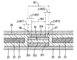
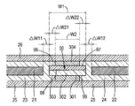
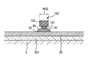
図1は第1の態様に係る磁気抵抗効果素子の一実施例を示す断面図である。図示実施例の磁気抵抗効果素子はGMR素子であり、GMR膜30と、電極膜25、26と、磁区制御膜21、22と、絶縁層23、24とを含む。
【0034】
GMR膜30は、フリ−層301を含み、膜厚方向の両面の少なくとも一面側に、幅方向の両端で落ち込むステップ部96、97を有する。図示実施例の磁気抵抗効果素子は、フリ−層301に隣接する非磁性層302を有し、非磁性層302の上に、ピンド層303が隣接している。ピンド層303の上には反強磁性層304が設けられている。ピンド層303は、反強磁性層304との交換結合により、磁化方向が固定される。
【0035】
反強磁性層304は、幅方向の両端で、ピンド層303の幅W1よりも、寸法差ΔW21、ΔW22だけ狭い幅W2を有しており、寸法差ΔW21、ΔW22によって、ステップ部96、97を生じさせてある。フリ−層301、非磁性層302、ピンド層303及び反強磁性層304の膜構造及び組成材料等については、既に知られている技術を、任意に適用できる。
【0036】
非磁性層302は、SV膜の場合はCu等を主成分とする導電性材料層で構成され、TMR膜の場合は、酸化アルミニウム層等の絶縁性材料層で構成される。
【0037】
電極膜25、26のそれぞれは、GMR膜30の両面に隣接する。実施例では、上部電極膜26が、ステップ部96−97間の面で反強磁性層304に隣接し、下部電極膜25がフリ−層301に隣接している。
【0038】
磁区制御膜21、22は、GMR膜30の幅方向の両側部に、間隔ΔW11、ΔW12を隔てて配置されている。磁区制御膜21、22は、フリ−層301の磁区を制御する。
【0039】
絶縁層23、24は、磁区制御膜21、22と、電極膜25、26及びGMR膜30との間を埋めている。具体的には、絶縁層23、24は、磁区制御膜21、22と電極膜25、26との間では、層状に配置され、磁区制御膜21、22とGMR膜30との間では、両者間に生じる間隔ΔW11、ΔW12を埋め、更に、ステップ部96、97を埋めるように形成されている。
【0040】
上述したように、本発明に係る磁気抵抗効果素子は、GMR膜30と、電極膜25、26とを含んでおり、電極膜25、26のそれぞれは、GMR膜30の両面に隣接している。したがって、GMR膜30の膜面に対して垂直方向にセンス電流を流す磁気抵抗効果素子を得ることができる。そのような磁気抵抗効果素子の例は、既に述べたように、CPPタイプのSV膜またはTMR膜である。
【0041】
CPPタイプのSV膜またはTMR膜は、少なくとも1つのフリ−層301を含んでおり、フリ−層301に発生することのあるバルクハウゼンノイズを抑制しなければならない。図示実施例の磁気抵抗効果素子は、磁区制御膜21、22を含んでおり、磁区制御膜21、22は、GMR膜30の幅方向の両側部に配置され、フリ−層301の磁区を制御する。したがって、バルクハウゼンノイズを抑制することができる。
【0042】
絶縁層23、24は、磁区制御膜21、22と、電極膜25、26との間に層状に介在し、GMR膜30との間では、両者間に生じる間隔ΔW11、ΔW12を埋めている。この構造によれば、電極膜25、26及びGMR膜30から磁区制御膜21、22へのセンス電流の漏洩を、絶縁層23、24によって、確実に防止することができる。
【0043】
GMR膜30は、膜厚方向の両面の少なくとも一面側に、幅方向の両端で落ち込むステップ部96、97を有しており、電極膜25、26はステップ部96−97間の面で、GMR膜30に隣接している。この構造によれば、センス電流が、主に、ステップ部96−97間の縮小された幅W2に対応する中央領域を通って流れることになるので、読み取りトラック幅を狭小化できる。しかも、絶縁層23、24が、ステップ部96、97に入るので、磁区制御膜21、22と上部電極膜26との間の電気絶縁性が更に向上する。
【0044】
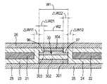
図2は第1の態様に係る磁気抵抗効果素子の別の実施例を示す断面図である。図において、図1に表れた構成部分と同一の構成部分については、同一の参照符号を付してある。この実施例では、ステップ部96、97は、反強磁性層304の幅方向の両端部に、反強磁性層304の表面からその膜厚内の段差をもって落ち込んでいる。この実施例の場合も図1に示したと同様の作用効果を奏する。
【0045】
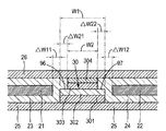
図3は第1の態様に係る磁気抵抗効果素子の更に別の実施例を示す断面図である。図において、図1に表れた構成部分と同一の構成部分については、同一の参照符号を付してある。この実施例では、ステップ部96、97は、反強磁性層304の表面から、ピンド層303に達し、その膜厚内で止まるような段差をもって落ち込む。この実施例の場合も図1に示したと同様の作用効果を奏する。
【0046】
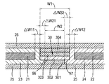
図4は第1の態様に係る磁気抵抗効果素子の更に別の実施例を示す断面図である。図において、図1に表れた構成部分と同一の構成部分については、同一の参照符号を付してある。この実施例では、ステップ部96、97は、反強磁性層304及びピンド層303の幅方向の両端を切り欠き、非磁性層302に達する段差をもって落ち込む。この実施例の場合も図1に示したと同様の作用効果を奏する。
【0047】
図5は第1の態様に係る磁気抵抗効果素子の更に別の実施例を示す断面図である。この実施例では、フリ−層301の両端にステップ部96、97を設けてある。電極膜25はステップ部96−97間の面で、フリ−層301に隣接している。この構造によれば、センス電流が、主に、ステップ部96−97間の縮小された幅W2に対応する中央領域を通って流れることになるので、読み取りトラック幅を狭小化できる。しかも、絶縁層23、24が、ステップ部96、97に入るので、磁区制御膜21、22と電極膜25との間の電気絶縁性が更に向上する。
【0048】
図6は第1の態様に係る磁気抵抗効果素子の更に別の実施例を示す断面図である。図において、図1に表れた構成部分と同一の構成部分については、同一の参照符号を付してある。この実施例では、反強磁性層304の両端にステップ部96、97を設けるとともに、フリ−層301の両端にもステップ部98、99を設けてある。上部電極膜26はステップ部96−97間の面で、反強磁性層304に隣接し、下部電極膜25はステップ部98−99間の面で、フリ−層301に隣接している。この構造によれば、センス電流が、主に、ステップ部96−97、及び、98−99間の縮小された幅W2に対応する中央領域を通って流れることになるので、読み取りトラック幅を狭小化できる。しかも、絶縁層23、24が、ステップ部96〜99に入るので、磁区制御膜21、22と電極膜25、26との間の電気絶縁性が更に向上する。
【0049】
図7は第1の態様に係る磁気抵抗効果素子の更に別の実施例を示す断面図である。この実施例では、フリ−層301の両端にステップ部96、97を設けてある。電極膜25はステップ部96−97間の面で、フリ−層301に隣接している。この構造は、図5の実施例と同じであリ、図5の実施例と同様に、センス電流が、主に、ステップ部96−97間の縮小された幅W2に対応する中央領域を通って流れることになるので、読み取りトラック幅を狭小化できる。しかも、絶縁層23、24が、ステップ部96、97に入るので、磁区制御膜21、22と電極膜25との間の電気絶縁性が更に向上する。図5の実施低例と異なる点は、磁区制御膜21,22が、電極膜26に隣接していることである。
【0050】
次に第2の態様に係る磁気抵抗効果素子について、図8〜図19を参照して説明する。図において、先に示した図面に現れた構成部分と同一の構成部分については同一の参照符号を付し、重複説明は、これを省略することがある。
【0051】
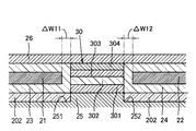
まず、図8は第2の態様に係る磁気抵抗効果素子の一実施例を示す断面図である。図示実施例の磁気抵抗効果素子は、GMR膜30と、一対の電極膜25,26と、磁区制御膜21,22と、絶縁層23,24、202とを含む。GMR膜30は、フリ−層301、非磁性層302、ピンド層303及び反強磁性層304を含む。非磁性層302はSV膜の場合、導電性非磁性層となり、TMR膜の場合、絶縁性非磁性層となることは前述したとおりである。
【0052】
電極膜25,26のそれぞれは、GMR膜30の膜厚方向の両面に隣接する。電極膜25,26のうち、電極膜25は、GMR膜30と隣接する部分に、幅方向の両端で落ち込むステップ部251,252を有する。ステップ部251,252は、この実施例では、電極25の幅方向両端が、GMR膜30の幅方向両端と同一位置となるよう形成されている。
【0053】
磁区制御膜21,22は、GMR膜30の幅方向の両側部に配置され、フリ−層301の磁区を制御する。
【0054】
絶縁層23,24,202は、磁区制御膜21,22と、電極膜25,26及びGMR膜30との間を埋めている。より詳しくは、絶縁膜202は、その表面が、電極膜25の表面位置とほぼ同じ高さ位置を保ち、同一の平面を構成するように、ステップ部251,252を埋めている。絶縁層23、24は、磁区制御膜21、22と、電極膜26及び絶縁膜202との間に層状に介在し、GMR膜30との間では、両者間に生じる間隔ΔW11、ΔW12を埋めている。
【0055】
上述したように、第2の態様に係る磁気抵抗効果素子は、GMR膜30と、電極膜25,26とを含んでおり、電極膜25,26のそれぞれは、GMR膜30の両面に隣接している。したがって、GMR膜30の膜面に対して垂直方向にセンス電流を流す磁気抵抗効果素子を得ることができる。そのような磁気抵抗効果素子の例は、CPPタイプのSV膜またはTMR膜であることは前述したとおりである。
【0056】
第2の態様に係る磁気抵抗効果素子も、磁区制御膜21,22を含んでおり、磁区制御膜21,22は、GMR膜30の幅方向の両側部に配置され、フリ−層301の磁区を制御する。したがって、バルクハウゼンノイズを抑制することができる。
【0057】
絶縁層23,24,202は、磁区制御膜21,22と、電極膜25,26及びGMR膜30との間を埋めている。この構造によれば、電極膜25,26及びGMR膜30から磁区制御膜21,22へのセンス電流の漏洩を、絶縁層23,24,202によって確実に防止することができる。
【0058】
電極膜25,26のうち、電極膜25は、GMR膜30と隣接する部分に、幅方向の両端で落ち込むステップ部251,252を有する。このようなステップ部251,252があると、絶縁層202が、ステップ部251,252に入り、ステップ部251,252に厚い絶縁層251,252が形成されるので、磁区制御膜21,22と、電極膜25との間の電気絶縁性が更に向上する。
【0059】
更に、ステップ部251,252の設計によって、電極膜25と、GMR膜30との間の接触面積を自由に調整することができる。例えば、後で説明するように、ステップ部251,252を、電極膜25と、GMR膜30との間に、GMR膜30の最大幅よりも狭幅の接触幅を生じさせるように設計した場合には、センス電流が、主に、ステップ部251−252間の縮小された幅に対応する中央領域を通って流れることになるので、読み取りトラック幅を狭小化できる。
【0060】
図8の実施例では、電極25,26のうち、電極25にのみ、ステップ部251,252を設けた例を示したが、電極25,26の何れか一方、または、両者にステップ部251,252を設けてもよい。
【0061】
図9は第2の態様に係る磁気抵抗効果素子の別の実施例を示す断面図である。図において、図8に表れた構成部分と同一の構成部分については、同一の参照符号を付し、重複説明は省略する。図示実施例では、電極膜25,26のうち、電極膜25が、GMR膜30と隣接する部分に、幅方向の両端で落ち込むステップ部251,252を有する他、反強磁性層304が、幅方向の両端で、ピンド層303の幅W1よりも、寸法差ΔW21、ΔW22だけ狭い幅W2を有しており、寸法差ΔW21、ΔW22によって、ステップ部96、97を生じさせてある。この実施例は、図1に示した第1の態様と、図8に示した第2の態様との組み合わせと観念することができる。従って、図1及び図8の実施例で説明した作用効果を、併せ得ることができる。
【0062】
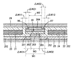
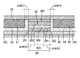
図10は第2の態様に係る磁気抵抗効果素子の更に別の実施例を示す断面図である。図示実施例では、電極膜25,26のうち、電極膜25が、GMR膜30と隣接する部分に、幅方向の両端で落ち込むステップ部251,252を有する。ステップ部251,252は、GMR膜30の最大幅W1よりも、寸法差ΔW31、ΔW32だけ狭い接触幅W3を生じさせるように付されている。このような構造であると、電極25の側では、センス電流が、主に、ステップ部251−252間の縮小された電極幅に対応する中央領域を通って流れることになるので、読み取りトラック幅を狭小化できる。
【0063】
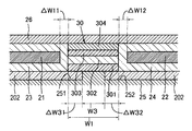
図11は第2の態様に係る磁気抵抗効果素子の更に別の実施例を示す断面図である。図示実施例では、電極膜25が、GMR膜30と隣接する部分に、幅方向の両端で落ち込むステップ部251,252を有する点では、図10の実施例と同様であるが、図10の実施例と異なって、反強磁性層304は、幅方向の両端で、GMR膜30の最大幅W1よりも、寸法差ΔW21、ΔW22だけ狭い幅W2を有しており、寸法差ΔW21、ΔW22によって、ステップ部96、97を生じさせてある。従って、電極膜26の側でも、センス電流が、主に、ステップ部96−97間の縮小された幅に対応する中央領域を通って流れることになるので、読み取りトラック幅を狭小化できる。
【0064】
図11の実施例は、図1に示した第1の態様と、図10に示した第2の態様との組み合わせと観念することができる。従って、図1および図10の実施例で説明した作用効果を、併せて得ることができる。
【0065】
図12は第2の態様に係る磁気抵抗効果素子の更に別の実施例を示す断面図である。図示実施例では、フリ−層301は、ステップ部251,252によって画定される電極膜25と同幅であり、幅方向の両端で、GMR膜30の最大幅W1よりも、寸法差ΔW31、ΔW32だけ狭い幅W3を有している。このような構造であると、センス電流が、更に、中央領域に集中するように流れることになるので、読み取りトラック幅を狭小化できる。
【0066】
図12の実施例は、図5に示した第1の態様と、図10に示した第2の態様との組み合わせと観念することもできる。従って、図5および図10の実施例で説明した作用効果を、併せて得ることができる。
【0067】
図13は第2の態様に係る磁気抵抗効果素子の更に別の実施例を示す断面図である。図示実施例では、フリ−層301は、ステップ部251,252によって画定される電極膜25と同幅であり、幅方向の両端で、GMR膜30の最大幅W1よりも、寸法差ΔW31、ΔW32だけ狭い幅W3を有しているのに加えて、反強磁性層304は、幅方向の両端で、GMR膜30の最大幅W1よりも、寸法差ΔW21、ΔW22だけ狭い幅W2を有しており、寸法差ΔW21、ΔW22によって、ステップ部96、97を生じさせてある。
【0068】
図13の実施例は、図1に示した第1の態様と、図12に示した第2の態様との組み合わせと観念することができる。従って、図1および図12の実施例で説明した作用効果を、併せて得ることができる。
【0069】
図14は第2の態様に係る磁気抵抗効果素子の更に別の実施例を示す断面図である。図示実施例では、磁区制御膜21,22が、電極膜26に隣接している。
【0070】
また、電極膜25,26のうち、電極膜25が、GMR膜30と隣接する部分に、幅方向の両端で落ち込むステップ部251,252を有する。ステップ部251,252は、GMR膜30の最大幅W1よりも、寸法差ΔW31、ΔW32だけ狭い接触幅W3を生じさせるように付されている。
【0071】
図14の実施例は、図7に示した第1の態様と、図10に示した第2の態様との組み合わせと観念することができる。従って、図7および図10の実施例で説明した作用効果を、併せて得ることができる。
【0072】
図15は第2の態様に係る磁気抵抗効果素子の更に別の実施例を示す断面図である。図示実施例では、磁区制御膜21,22が、電極膜26に隣接している。
【0073】
また、電極膜25,26のうち、電極膜25が、GMR膜30と隣接する部分に、幅方向の両端で落ち込むステップ部251,252を有する。ステップ部251,252は、電極25の幅方向両端が、GMR膜30の幅方向両端と同一位置となるよう形成されている。
【0074】
図15の実施例は、図7に示した第1の態様と、図8に示した第2の態様との組み合わせと観念することができる。従って、図7および図8の実施例で説明した作用効果を、併せて得ることができる。
【0075】
図16は第2の態様に係る磁気抵抗効果素子の更に別の実施例を示す断面図である。図示実施例では、磁区制御膜21,22が、電極膜26に隣接している。
【0076】
また、電極膜25,26のうち、電極膜25が、GMR膜30と隣接する部分に、幅方向の両端で落ち込むステップ部251,252を有する。フリ−層301は、ステップ部251,252によって画定される電極膜25と同幅であり、幅方向の両端で、GMR膜30の最大幅W1よりも、寸法差ΔW31、ΔW32だけ狭い幅W3を有している。
【0077】
絶縁膜202は、フリ−層301と非磁性層302との境界と、同一の平面を構成するように、ステップ部251,252を埋めている。
【0078】
図16の実施例は、図7に示した第1の態様と、図12に示した第2の態様との組み合わせと観念することができる。従って、図7および図12の実施例で説明した作用効果を、併せて得ることができる。
【0079】
2.薄膜磁気ヘッド
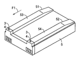
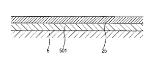
図17は本発明に係る薄膜磁気ヘッドの斜視図、図18は図17に示した薄膜磁気ヘッドの電磁変換素子部分の拡大断面図、図19は図18の19−19線に沿った断面図、図20は図19の拡大図である。何れの図面においても、寸法、プロポ−ション等は、図示の都合上、誇張されまたは省略されている。図示された薄膜磁気ヘッドは、スライダ基体5と、電磁変換素子3、4とを含む。スライダ基体5は、媒体対向面に浮上特性制御用の幾何学的形状を有している。そのような幾何学的形状の代表例として、実施例では、レ−ル51、52を示してある。レ−ル51、52の表面は、空気ベアリング面(以下ABSと称する)53、54となる。レ−ル51、52の形状は、図示の単純な直線状輪郭の他、複雑な輪郭や、負圧を発生される輪郭など多種、多様であり、本発明には何れも適用できる。スライダ基体5は、例えば、アルティック(Al2O3−TiC)等のセラミック材料からなる。
【0080】
図18〜図20を参照すると、スライダ基体1の端面には絶縁層501が設けられている。絶縁層501は、例えば、アルミナ(Al2O3)、SiO2等の絶縁材料からなり、1〜5μmの厚みである。
【0081】
電磁変換素子3、4は、再生素子を構成する磁気抵抗効果素子3と、記録素子4とを含む。再生素子を構成する磁気抵抗効果素子3は、SV膜またはTMR膜を含んでいる。SV膜の場合は、膜面に垂直に電流を流すCPP−GMRが用いられる。TMR膜は、本来、膜面に垂直にセンス電流を流すものである。
【0082】
記録素子4は、例えば、誘導型磁気変換素子あり、書き込み用磁極端がABS53、54に面している。記録素子4は、再生素子を構成する磁気抵抗効果素子3と近接して配置され、保護膜49によって覆われている。
【0083】
記録素子4は、下部磁極層41と、上部磁極層45と、記録ギャップ層42と、薄膜コイル43、47とを含む。下部磁極層41は上部シ−ルド層41として兼用されている。
【0084】
下部磁極層41は、上部シ−ルドギャップ層46の上に形成され、上部磁極層45と磁気的に連結されている。記録ギャップ層42は下部磁極層41の磁極部分と、上部磁極層45の磁極部分との間に設けられている。薄膜コイル43、47は下部磁極層41及び上部磁極層45の間のインナーギャップ間の絶縁層48内に、絶縁された状態で配設されている。
【0085】
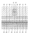
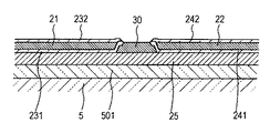
再生素子を構成する磁気抵抗効果素子3は、GMR膜30と、電極膜25、26と、下部シ−ルド層28と、下部シールドギャップ層201と、上部シ−ルドギャップ層46とを含む。図示実施例の磁気抵抗効果素子3は、更に、磁区制御膜21、22と、絶縁層(231、232)、(241、242)とを含む。
【0086】
下部シ−ルド層28は、パーマロイ(NiFe)等の磁性材料よりなり、絶縁層501の上に、スパッタリング法またはめっき法等によって、例えば約3μmの厚みとなるように形成されている。
【0087】
下部シールドギャップ層201は、下部シ−ルド層28の上に備えられている。下部シールドギャップ層201は、アルミナ等の絶縁材料よりなり、スパッタ等によって、例えば10〜200nmの厚みに形成されている。
【0088】
下部電極膜25は、例えば、数十nmの厚みをもって、下部シールドギャップ層201の上に形成されている。下部電極膜25は、GMR膜30と隣接すべき部分が、突出しており、その突出部分の両側に生じる凹部は絶縁層202によって埋められている。絶縁層202の表面は下部電極膜25の表面と同一平面を構成している。絶縁層202は、アルミナ(Al2O3)、SiO2等の絶縁材料からなる。
【0089】
図20を参照すると、GMR膜30は、フリ−層301を含み、膜厚方向の両面の少なくとも一面側に、幅方向の両端で落ち込むステップ部96、97を有する。図示実施例の磁気抵抗効果素子は、フリ−層301に隣接する非磁性層302を有し、非磁性層302の上に、ピンド層303が隣接している。ピンド層303の上には反強磁性層304が設けられている。ピンド層303は、反強磁性層304との交換結合により、磁化方向が固定される。
【0090】
反強磁性層304は、幅方向の両端で、ピンド層303の幅W1よりも狭い幅W2を有しており、寸法差によって、間隔ΔW21、ΔW22のステップ部96、97を生じさせてある。フリ−層301、非磁性層302、ピンド層303及び反強磁性層304の膜構造及び組成材料等については、既に知られている技術を、任意に適用できる。一例をあげると、フリ−層301及びピンド層303は、例えば、NiFe、NiFeCo、CoFe等で構成され、反強磁性層304はFeMn、MnIr、NiMn、CrMnPtなどによって構成される。
【0091】
非磁性層302は、SV膜の場合はCu等を主成分とする導電性材料層で構成され、TMR膜の場合は、酸化アルミニウム層などの絶縁性材料層で構成される。
【0092】
上部電極膜26は、ステップ部96−97間の面で反強磁性層304に隣接し、下部電極膜25がフリ−層301に隣接している。
【0093】
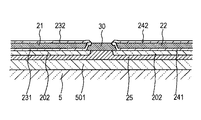
磁区制御膜21、22は、GMR膜30の幅方向の両側部に、絶縁層(231、232)、(241、242)による間隔を隔てて配置されている。磁区制御膜21、22は、フリ−層301の磁区を制御する。
【0094】
絶縁層(231、232)、(241、242)は、磁区制御膜21、22と、電極膜25、26及びGMR膜30との間を埋めている。具体的には、絶縁層(231、232)、(241、242)は、磁区制御膜21、22と電極膜25、26との間では、層状に配置され、磁区制御膜21、22とGMR膜30との間では、両者間に生じる間隔ΔW11、ΔW12を埋め、更に、ステップ部96、97を埋めるように形成されている。
【0095】
上部電極膜26は上部シ−ルドギャップ層46によって覆われている。上部シ−ルドギャップ層46は、アルミナ等の絶縁材料からなり、スパッタ等によって、例えば10〜200nmの厚み(最小厚み)に形成されている。
【0096】
上部シ−ルド層41は、パーマロイ(NiFe)等の磁性材料よりなり、上部シ−ルドギャップ層46の上に、スパッタリング法またはめっき法等によって、例えば約3μmの厚みとなるように形成されている。実施例では、上部シ−ルド層41は、記録素子4の下部磁性層として兼用されている。
【0097】
上述した薄膜磁気ヘッドにおいて、GMR膜30と、電極膜25、26とを含んでおり、電極膜25、26のそれぞれは、GMR膜30の両面に隣接している。したがって、GMR膜30の膜面に対して垂直方向にセンス電流を流す磁気抵抗効果素子3を得ることができる。そのような磁気抵抗効果素子3の例は、既に述べたように、CPPタイプのSV膜またはTMR膜である。
【0098】
CPPタイプのSV膜またはTMR膜は、少なくとも1つのフリ−層301を含んでおり、フリ−層301に発生することのあるバルクハウゼンノイズを抑制しなければならない。図示実施例の磁気抵抗効果素子は、磁区制御膜21、22を含んでおり、磁区制御膜21、22は、GMR膜30の幅方向の両側部に配置され、フリ−層301の磁区を制御する。したがって、バルクハウゼンノイズを抑制することができる。
【0099】
絶縁層(231、232)、(241、242)は、磁区制御膜21、22と、電極膜25、26との間に層状に介在し、GMR膜30との間では、両者間に生じる間隔ΔW11、ΔW12を埋めている。この構造によれば、電極膜25、26及びGMR膜30から磁区制御膜21、22へのセンス電流の漏洩を、絶縁層(231、232)、(241、242)によって、確実に防止することができる。
【0100】
GMR膜30は、膜厚方向の両面の少なくとも一面側に、幅方向の両端で落ち込むステップ部96、97を有しており、電極膜25、26はステップ部96−97間の面で、GMR膜30に隣接している。この構造によれば、センス電流が、主に、ステップ部96−97間の縮小された幅W2に対応する中央領域を通って流れることになるので、読み取りトラック幅を狭小化できる。しかも、絶縁層(231、232)、(241、242)が、ステップ部96、97に入るので、磁区制御膜21、22と上部電極膜26との間の電気絶縁性が更に向上する。
【0101】
上記実施例の薄膜磁気ヘッドは、図1〜図16に示した膜構造のうち、図11に示したものを適用したものであるが、図1〜図10、図12〜図16に示した膜構造も同様に適用できる。
【0102】
3.磁気ヘッド装置
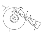
図21は本発明に係る磁気ヘッド装置の正面図、図22は図21に示した磁気ヘッド装置の底面図である。図示された磁気ヘッド装置は、図17〜図20に示した薄膜磁気ヘッド40と、ヘッド支持装置5とを含む。ヘッド支持装置5は、金属薄板でなる支持体51の長手方向の一端にある自由端に、同じく金属薄板でなる可撓体52を取付け、この可撓体52の下面に薄膜磁気ヘッド40を取付けた構造となっている。
【0103】
具体的には、可撓体52は、支持体51の長手方向軸線と略平行して伸びる2つの外側枠部521、522と、支持体51から離れた端において外側枠部521、522を連結する横枠523と、横枠523の略中央部から外側枠部521、522に略平行するように延びていて先端を自由端とした舌状片524とを有する。横枠523のある方向とは反対側の一端は、支持体51の自由端付近に溶接等の手段によって取付けられている。
【0104】
支持体51の下面には、例えば半球状の荷重用突起525が設けられている。この荷重用突起525により、支持体51の自由端から舌状片524へ荷重力が伝えられる。
【0105】
薄膜磁気ヘッド40は、舌状片524の下面に接着等の手段によって取付けられている。薄膜磁気ヘッド40は、ピッチ動作及びロール動作が許容されるように支持されている。
【0106】
本発明に適用可能なヘッド支持装置5は、上記実施例に限定するものではなく、これまで提案され、またはこれから提案されることのあるヘッド支持装置を、広く適用できる。例えば、支持体51と舌状片524とを、タブテープ(TAB)等のフレキシブルな高分子系配線板を用いて一体化したもの等を用いることもできる。また、従来より周知のジンバル構造を持つものを自由に用いることができる。
【0107】
4.磁気記録再生装置
図23は図21、図22に示した磁気ヘッド装置を用いた磁気記録再生装置の平面図である。図示された磁気記録再生装置は、図21、図22に示した磁気ヘッド装置6と、位置決め装置8と、磁気ディスク7とを含む。位置決め装置8は、ロータリ・アクチュエータ方式であり、ヘッド支持装置5の他端側を支持している。
【0108】
本実施例において、磁気ディスク7は磁気ヘッド装置6と協働して磁気記録再生を行う。磁気ディスク7は、図示しない回転駆動機構により、矢印F1の方向に高速で回転駆動される。
【0109】
薄膜磁気ヘッド40は、ヘッド支持装置5及び位置決め装置8により、矢印B1またはB2の方向に駆動され、所定のトラック上で、磁気ディスク7への書き込み及び読み出しを行う。
【0110】
5.薄膜磁気ヘッドの製造方法
次に、本発明に係る薄膜磁気ヘッドの製造方法の第1態様について、図24〜図36を参照して説明する。この製造方法は磁気抵抗効果素子の製造にも適用できる。
【0111】
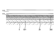
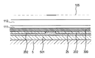
まず、図24に示すように、スライダ基体5の上に、絶縁層501を形成し、更に絶縁層501の上に下部電極膜25を形成する。下部電極層を構成する導電層25を、下部シールド層から独立して設ける場合は、図18、図19に例示したように、絶縁層501、下部シ−ルド層28及び下部シールドギャップ層201を形成し、更に下部シールドギャップ層201の上に下部電極膜となる導電層25を形成する。
【0112】
次に、図25に示すように、下部電極膜25上に、再生用のGMR素子となる被パタ−ンニング層300を形成する。図では、被パタ−ンニング層300は単層表示であるが、実際のSV膜またはTMR膜では、図1〜図16に示したように、多層膜構造となる。
【0113】
次に、図26に示すように、被パタ−ンニング層300の上に、下層レジスト層111を形成し、更に、下層レジスト層111の上に上層レジスト層112を形成する。下層レジスト層111は、スピンコート法等の手段によって塗布した後、必要に応じて、これを加熱することによって形成される。
【0114】
下層レジスト層111を構成するレジスト材料は、その上に形成される上層レジスト層112を構成するレジスト材料とインターミキシングを起こさない材料であることが必要である他、アンダーカットの入った積層(2層)レジストパターンを形成する場合は、採用されるアンダーカット形成方法に適した材料が選択される。アンダーカット形成方法としては、現像剤のみによる方法、アッシングのみによる方法、及び、現像剤とアッシングとを併用する方法がある。
【0115】
この内、現像のみでアンダーカットの入った2層レジストパターンを形成する場合は、下層レジスト層111を構成するレジスト材料は、現像剤として通常用いられるアルカリ性水溶液に溶解し、かつ、上層レジスト層(後述)よりもアルカリ性水溶液による溶解速度の速い材料によって構成する。この場合の具体例としては、ポリメチルグルタールイミド(以下PMGIと称する)を挙げることができる。
【0116】
アッシングのみでアンダーカットの入った2層レジストを得る場合は、アッシング反応速度が、上層レジスト層(後述)を構成するレジスト材料よりも速いこと等の条件を満たす材料を用いる。
【0117】
現像剤とアッシングとを併用してアンダーカットを入れる場合は、アルカリ性水溶液に溶解し、かつ、アッシング反応速度が上層レジスト層(後述)を構成するレジスト材料よりも速いこと等の条件を満たす材料を用いる。
【0118】
上層レジスト層112は、フェノール性水酸基を含むレジストを主成分とするものが好ましい。上層レジスト層112に適したフェノール性水酸基を含むレジストの例としては、特公昭37−18015号公報に開示されたNQD−ノボラックレジスト(ナフトキノンジアジド−ノボラックレジスト)、特開平6−242602号公報に開示された一体型NQD−ノボラックレジスト、特開2000−63466号公報に開示された疎水性一体型NQD−ノボラックレジスト、及び、特開平6−273934号公報に開示されたポリヒドロキシスチレン系樹脂を主成分とした化学増幅型レジスト等を挙げることができる。
【0119】
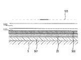
次に、図27に示すように、マスク105を介して、上層レジスト層112を露光して、上層レジスト層112にマスク105のパターンに従った潜像を形成する。露光用の光は、紫外線、エキシマレーザー光、電子ビーム等、どのような光でもよい。露光用の光が電子線である場合には、マスク105を介することなく、直接、上層レジスト層112に電子線を照射することにより、所定のパターンの潜像を形成してもよい。また、必要に応じて、露光後に上層レジスト層112を加熱する。
【0120】
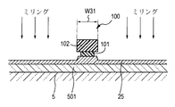
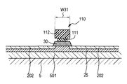
次に、図28に示すように、現像液によって、露光後の上層レジスト層112を現像すると共に、下層レジスト層111の一部を溶解させる。現像後、下層レジスト層111および上層レジスト層112の水洗と乾燥を行う。これにより、アンダーカットの入ったレジストマスク110が得られる。アンダーカットの入ったレジストマスク110では、上層レジスト層112は、下層の下層レジスト層111の平面積よりも大きい幅W31を有する。このようなレジストマスク110は、パターンの微細化に有効である。現像液としては、テトラメチルアンモニウムハイドロオキサイド(TMAH)の水溶液等のアルカリ性水溶液を用いることが好ましい。
【0121】
次に、図29に示すように、例えばイオンミリング等のドライエッチングによって、被パタ−ンニング層300を選択的にエッチングし、GMR膜30を形成する。
【0122】
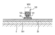
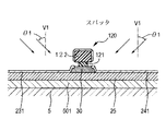
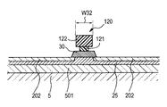
次に、図30に示すように、レジストマスク110の幅W31よりも狭い幅W32のレジストマスク120を形成する。このレジストマスク120も、レジストマスク110と同様に、アンダーカットの入ったレジストパターン121、122である。レジストパタ−ン120は、レジストパターン110をアッシングなどの手段によってスリム化して得ることもできるし、レジストパタ−ン110を形成するときのプロセスを、再度、実行することによっても、得ることができる。
【0123】
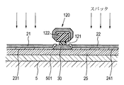
次に、図31に示すように、例えばイオンミリング等のドライエッチングによって、GMR膜30の表面を選択的にエッチングし、ステップ部96、97を形成する。
【0124】
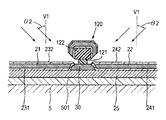
次に、図32に示すように、レジストマスク120を残したままで、例えば、スッパタ等の薄膜形成プロセスを実行することにより、絶縁層231、241を成膜する。絶縁層231、241はAl2O3などの絶縁材料でなる。この薄膜形成プロセスにおいては、指向性を持つイオン.ビーム.ディポジッション(以下IBDと称する)方法を適用する。具体的には、膜面に垂直な垂線V1に対して、角度θ1をもつ指向性スパッタを実行し、絶縁層231、241を、レジストパターン122の下側に形成されているアンダーカット部分に侵入させる。これにより、絶縁層231、241はステップ部96、97を埋めるように付着される。
【0125】
次に、図33に示すように、レジストマスク120を残したままで、絶縁層231、241の上に磁区制御膜21、22を、スパッタなどの手段によって成膜する。このときのスパッタは、膜面に対してほぼ直交する方向に行う。このため、磁区制御膜21、22は、レジストパターン122の下側のアンダーカット部分には入らず、絶縁層231、241のうち、アンダーカット部分において、ステップ部を埋めている部分は、磁区制御膜21、22が成膜されず、絶縁層231、241が露出している。
【0126】
次に、図34に示すように、レジストマスク120を残したままで、例えば、スッパタ等の薄膜形成プロセスを実行することにより、絶縁層232、242を成膜する。絶縁層232、242はAl2O3などの絶縁材料でなる。この薄膜形成プロセスにおいても、指向性を持つIBDを適用する。具体的には、膜面に垂直な垂線V1に対して、角度θ2をもつ指向性スパッタを実行し、絶縁層232、242を、レジストパターン122の下側に形成されているアンダーカット部分に侵入させる。これにより、絶縁層232、242は、先に成膜されている絶縁層231、241と、アンダーカットの部分で連続することになる。
【0127】
次に、図35に示すように、レジストマスク120を剥離し、除去する。レジストマスク120の剥離に当たってはアセトン等の有機溶剤を用いることができる。
【0128】
次に、図36に示すように、上部電極膜26を成膜し、更に、記録ヘッドのための製造プロセスを実行する。記録ヘッドの製造プロセスは周知である。
【0129】
次に、本発明に係る薄膜磁気ヘッドの製造方法の第2態様について、図37〜図53を参照して説明する。図において、第1態様において表れた構成部分と同一の構成部分については、同一の参照符号を付し、重複説明は省略する。この製造方法は磁気抵抗効果素子の製造にも適用できる。
【0130】
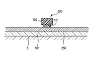
まず、図37に示すように、スライダ基体5の上に、絶縁層501を形成し、更に絶縁層501の上に下部電極膜となる導電層250を形成する。
【0131】
図示の場合、下部電極膜を構成する導電層250は、下部シールド層として兼用される。導電層250を、下部シールド層として兼用する場合は、例えば、NiFe、CoFeNi、CoFeなどの軟磁性材料を用いる。これとは異なって、図18、図19に例示したように、下部電極層を構成する導電層250を、下部シールド層から独立して設ける場合は、絶縁層501、下部シ−ルド層28及び下部シールドギャップ層201を形成し、更に下部シールドギャップ層201の上に下部電極膜となる導電層250を形成する。
【0132】
次に、図38に示すように、導電層250の上に、所定パターンをもつレジストマスク100を形成する。レジストマスク100は、下層レジスト層101の上に、その平面積よりも大きい幅を有する上層レジスト層102を積層したアンダーカット構造を有する。アンダーカットの入ったレジストマスク100は、パターンの微細化に有効である。レジストマスク100は、後で述べるパターニング方法の適用によって形成できる。
【0133】
次に、図39に示すように、例えばイオンミリング、リアクティブ.イオン.エッチング(RIE)等のドライエッチングによって、導電層250を選択的にエッチングし、下部電極膜25を形成する。
【0134】
次に、図40に示すように、レジストマスク100を残したままで、例えば、スッパタ等の薄膜形成プロセスを実行することにより、絶縁層202を成膜する。絶縁層202はAl2O3などの絶縁材料でなる。
【0135】
次に、図41に示すように、レジストマスク100を有機溶剤を用いて剥離し、下部電極膜25の中央に設けられた凸部の表面と、絶縁層202の表面が同一の平面を構成するように平坦化処理を行う。平坦化処理は、例えばCMP法の適用によって実行できる。
【0136】
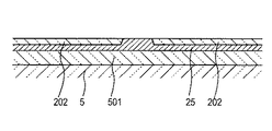
次に、図42に示すように、下部電極膜25及び絶縁層202の作る平面上に、再生用のGMR素子となる被パタ−ンニング層300を形成する。
【0137】
次に、図43に示すように、被パタ−ンニング層300の上に、下層レジスト層111を形成し、更に、下層レジスト層111の上に上層レジスト層112を形成する。
【0138】
次に、図44に示すように、マスク105を介して、上層レジスト層112を露光して、上層レジスト層112にマスク105のパターンに従った潜像を形成する。
【0139】
次に、図45に示すように、現像液によって、露光後の上層レジスト層112を現像すると共に、下層レジスト層111の一部を溶解させる。現像後、下層レジスト層111および上層レジスト層112の水洗と乾燥を行う。これにより、アンダーカットの入ったレジストマスク110が得られる。アンダーカットの入ったレジストマスク110では、上層レジスト層112は、下層の下層レジスト層111の平面積よりも大きい幅W31を有する。
【0140】
次に、図46に示すように、例えばイオンミリング等のドライエッチングによって、被パタ−ンニング層300を選択的にエッチングし、GMR膜30を形成する。
【0141】
次に、図47に示すように、レジストマスク110の幅W31よりも狭い幅W32のレジストマスク120を形成する。このレジストマスク120も、レジストマスク110と同様に、アンダーカットの入ったレジストパターン121、122である。
【0142】
次に、図48に示すように、例えばイオンミリング等のドライエッチングによって、GMR膜30の表面を選択的にエッチングし、ステップ部96、97を形成する。
【0143】
次に、図49に示すように、レジストマスク120を残したままで、例えば、スッパタ等の薄膜形成プロセスを実行することにより、絶縁層231、241を成膜する。
【0144】
次に、図50に示すように、レジストマスク120を残したままで、絶縁層231、241の上に磁区制御膜21、22を、スパッタなどの手段によって成膜する。このときのスパッタは、膜面に対してほぼ直交する方向に行う。このため、磁区制御膜21、22は、レジストパターン122の下側のアンダーカット部分には入らず、絶縁層231、241のうち、アンダーカット部分において、ステップ部を埋めている部分は、磁区制御膜21、22が成膜されず、絶縁層231、241が露出している。
【0145】
次に、図51に示すように、レジストマスク120を残したままで、例えば、スッパタ等の薄膜形成プロセスを実行することにより、絶縁層232、242を成膜する。
【0146】
次に、図52に示すように、レジストマスク120を剥離し、除去する。レジストマスク110の剥離に当たってはアセトン等の有機溶剤を用いることができる。
【0147】
次に、図53に示すように、上部電極膜26を成膜し、更に、記録ヘッドのための製造プロセスを実行する。記録ヘッドの製造プロセスは周知である。
【0148】
次に、実施例を挙げて、図37〜図53のプロセスを更に具体的に説明する。
(1)図37のプロセス
図37に示すプロセスにおいて、スライダ基体5として、直径3インチ、厚み2mmのAlTiC(アルティック)を用いた。このスライダ基体5の上に、Al2O3でなる絶縁層501を、厚さ3μmとなるようにスパッタした。その後、公知のフレームめっき法により、厚さ3μmのNiFeのめっき膜でなる導電膜250を成膜した。このNiFeめっき膜は、下部シールド層28(図18〜図20参照)として兼用される。絶縁層501のスパッタプロセス条件は次の通りである。
スパッタ装置:アルカテル社製 HEDA2480(RFバイアススパッタ)
スパッタ条件
スパッタ膜 Al2O3
ターゲット Al2O3
Power 15(kW)(13.56MHz)
バイアスVdc −150(V)
Arガス圧力 1(mTorr)
Arガス流量 100sccm
なお、流量単位sccmとは、standard cubic cmの略語であり、圧力を1気圧(1.01325×10⁵Pa)に変換した時の1分間当たりのcm3単位の流量を表す。
【0149】
(2)図38のプロセス
図38のプロセスにおいて、レジストマスク100は、PMGIを用いたアンダーカット入りの2層構造とした。その成膜プロセス条件は、次の通りである。
(a)PMGI塗布条件
PMGIとしては、シプレイファーイースト社製のLOL−500を用い、スピンコートにて、50nmの厚さに塗布し、次にプリベークした。プリベーク条件は180℃、300秒とした。
(b)レジストプリント条件
レジストとして、クラリアンジャパン社製のAZ510Pを用い、スピンコ−トにより0.25μmの厚さに塗布し、次にプリベークした。プリベーク条件は120℃、60秒とした。
(c)露光条件
露光装置として、ニコン社製NSR−TFHEX14Cを用いた。露光条件は次のとおりである。
NA;0.6
σ;0.75
Dose;30mJ/cm2
焦点;0μm
マスクサイズ;0.2μm
(d)現像条件
120℃の温度で60秒間加熱した。次に、現像液として、2.38%テトラメチルアンモニウムハイドロオキサイド(TMAH)の水溶液を用い、30秒、1パドルで、現像処理を行った。
【0150】
上述したプロセスを経ることにより、図38において、クリティカルパターン部分のレジスト幅0.12μm、長さ3μmで、両側に3μmだけ飛び出るアンダーカット入りのレジストマスク100を得た。レジストマスク100は、スライダ基体5をウエハーとしてその面上に多数整列して形成される。
【0151】
(3)図39のプロセス
下部電極膜25を得るに当たり、その導電層250をミリングした。ミリング装置は、Veeco 社製 IBE−IBDである。ミリング条件は次のとおりである。
ガス;Ar
ガス流量;10sccm
圧力:2×10⁻⁴Torr
ミリング角度:5°(膜面垂線に対する角度)
ビーム電流:300mA
ビーム電圧:DC300V
加速電圧:−500V
これにより、図39に示す下部電極膜25が得られた。ミリング深さは0.1μmである。
【0152】
(4)図40のプロセス
図40の絶縁膜202のスパッタ成膜は、次の条件で行った。
スパッタ装置:アルカテル社製 HEDA2480(RFバイアススパッタ)
スパッタ膜:Al2O3
ターゲット:Al2O3
Power:15(kW)(13.56MHz)
バイアスVdc:−150(V)
Arガス圧力:1(mTorr)
Arガス流量:100sccm
【0153】
(5)図41のプロセス
50℃のNMP(N−メチルピロリドン)中に、1時間、揺動を与えながら浸漬し、レジストマスク100を溶解除去した。日立製作所製 CD−SEM S7800により、目的のクリティカルパターン部分に形成された金属パターンを観察したところ、0.1μm幅のNiFe孤立ラインパターンの外側に、その境界にバリのないアルミナパターンが存在するNiFe−Al2O3連続パターンが得られた。
【0154】
(6)図42のプロセス
図42のプロセスでは、公知の手段にしたがって、TMR膜を得るための膜構造を有する被パターンニング膜300を成膜した。
【0155】
(7)図43〜図45のプロセス
図43、図44のプロセスにおいて、下層レジスト層111として、PMGIを用い、その上に上層レジスト層112となるレジストをプリントした。そのプロセス条件は、次の通りである。
(a)PMGI塗布条件
PMGIとしては、シプレイファーイースト社製のLOL−500を用い、スピンコートにて、50nmの厚さに塗布し、次にプリベークした。プリベーク条件は180℃、300秒とした。
(b)レジストプリント条件
レジストとして、クラリアンジャパン社製のAZ510Pを用い、スピンコ−トにより0.25μmの厚さに塗布し、次にプリベークした。プリベーク条件は120℃、60秒とした。
(c)露光条件
露光装置として、ニコン社製NSR−TFHEX14Cを用いた。露光条件は次のとおりである。
NA;0.6
σ;0.75
Dose;27mJ/cm2
焦点;0μm
マスクサイズ;0.2μm
(d)現像条件
120℃の温度で60秒間加熱した。次に、現像液として、2.38%テトラメチルアンモニウムハイドロオキサイド(TMAH)の水溶液を用い、30秒、1パドルで、現像処理を行った。
【0156】
上述したプロセスを経ることにより、図45において、クリティカルパターン部分のレジスト幅0.14μm、長さ3μmで、両側に3μmだけ飛び出るアンダーカット入りのレジストマスク110を得た。レジストマスク110は、スライダ基体5をウエハーとしてその面上に多数整列して形成される。
【0157】
(8)図46のプロセス
TMR膜を得るための膜構造と有する被パターンニング膜300を、レジストマスク110をマスクとしてミリングした。ミリング装置は、Veeco 社製
IBE−IBDである。ミリング条件は次のとおりである。
ガス;Ar
ガス流量;10sccm
圧力:2×10⁻⁴Torr
ミリング角度:5°(膜面垂線に対する角度)
ビーム電流:300mA
ビーム電圧:DC300V
加速電圧:−500V
これにより、図46のTMR膜でなるGMR膜30が得られた。GMR膜30の幅W31は0.12μmである。
【0158】
(9)図47のプロセス
図46のミリングプロセスを経て、幅W31が0.12μmとなっていたレジストマスク120を下記の条件でスリンミングし、その幅W32を0.1μmとした。
アッシング装置:Matrix inc. 社製 System 104
圧力:1.0Torr(約133Pa)
ガス:O2
ガス流量:30sccm
RF出力:200W
基板温度:70℃
【0159】
(10)図48のプロセス
図47のプロセスの後、ミリングによって、GMR膜30の表面を選択的にエッチングし、ステップ部96、97を形成した。ステップ部96、97の深さは、表面層から次の層に達するようにした。ミリング装置は、Veeco 社製 IBE−IBDである。ミリング条件は次のとおりである。
ガス;Ar
ガス流量;10sccm
圧力:2×10⁻⁴Torr
ミリング角度:5°(膜面垂線に対する角度)
ビーム電流:300mA
ビーム電圧:DC300V
加速電圧:−500V
【0160】
(11)図49のプロセス
アルミナ(Al2O3)を0.01μmの厚さにスパッタし、絶縁層231、241を成膜した。スパッタ装置は、Veeco 社製 IBE−IBDである。スパッタ条件は次のとおりである。
ガス;Ar
ガス流量;10sccm
圧力:2×10⁻⁴Torr
スパッタ角度θ1:45°(膜面垂線V1に対する角度)
ビーム電流:300mA
ビーム電圧:DC1500V
加速電圧:−200V
ターゲット:Al2O3
【0161】
(12)図50のプロセス
PtMnを0.02μmの厚さにスパッタし、磁区制御膜21、22を成膜した。スパッタ装置は、Veeco 社製 IBE−IBDである。スパッタ条件は次のとおりである。
ガス;Ar
ガス流量;10sccm
圧力:2×10⁻⁴Torr
スパッタ角度:10°(膜面垂線に対する角度)
ビーム電流:300mA
ビーム電圧:DC1500V
加速電圧:−200V
ターゲット:PtMn
【0162】
(13)図51のプロセス
アルミナ(Al2O3)を0.01μmの厚さにスパッタし、絶縁層232、242を成膜した。スパッタ装置は、Veeco 社製 IBE−IBDである。スパッタ条件は次のとおりである。
ガス;Ar
ガス流量;10sccm
圧力:2×10⁻⁴Torr
スパッタ角度θ2:45°(膜面垂線V1に対する角度)
ビーム電流:300mA
ビーム電圧:DC1500V
加速電圧:−200V
ターゲット:Al2O3
【0163】
(14)図52のプロセス
次に、50℃のNMP(N−メチルピロリドン)中に、1時間、揺動を与えながら浸漬し、レジストマスク120を溶解除去した。これにより、図52に示す所望パターンを有するGMR膜30が得られた。
【0164】
図52のGMR膜30を、日立製作所製 CD−SEM S7800により観察したところ、0.1μm幅のTMR膜の孤立ラインパターンの外側に、バリのないアルミナによる絶縁層232、242が連続する連続パターンが得られていることが確認された。
【0165】
(15)図53のプロセス
公知のフレームめっき法により、厚さ3μmのNiFe膜を形成し、上部電極膜26とした。
【0166】
上述したプロセスによって得られるGMR膜30の幅は0.12μmであり、上電極膜26がGMR膜30に接している幅は0.1μmであり、実効読み取り幅は0.1μmであった。
【0167】
図示及び説明は省略するが、本発明は、SV膜に対して、膜面に垂直に電流を流すCPP−GMR素子を有する薄膜磁気ヘッドの製造にも、若干のプロセス修正を加えることにより、適用できることは明らかである。
【0168】
本発明は、上記実施の形態に限定されず種々の変更が可能である。例えば、本発明は、半導体デバイスや、薄膜を用いたセンサやアクチュエータ等、薄膜磁気ヘッド以外のマイクロデバイスの製造方法にも適用することができる。
【0169】
【発明の効果】
以上述べたように、本発明によれば、次のような効果を得ることができる。
(a)センス電流漏洩を確実に防止できるとともに、狭トラック化にも容易に対応できる磁気抵抗効果素子、薄膜磁気ヘッド、磁気ヘッド装置及び磁気記録再生装置を提供することができる。
(b)上述した磁気抵抗効果素子もしくは薄膜磁気ヘッドを製造するのに適した製造方法を提供することができる。
【図面の簡単な説明】
【図1】図1は発明に係る磁気抵抗効果素子の一実施例を示す断面図である。
【図2】本発明に係る磁気抵抗効果素子の別の実施例を示す断面図である。
【図3】本発明に係る磁気抵抗効果素子の更に別の実施例を示す断面図である。
【図4】本発明に係る磁気抵抗効果素子の更に別の実施例を示す断面図である。
【図5】本発明に係る磁気抵抗効果素子の更に別の実施例を示す断面図である。
【図6】本発明に係る磁気抵抗効果素子の更に別の実施例を示す断面図である。
【図7】本発明に係る磁気抵抗効果素子の更に別の実施例を示す断面図である。
【図8】本発明に係る磁気抵抗効果素子の更に別の実施例を示す断面図である。
【図9】本発明に係る磁気抵抗効果素子の更に別の実施例を示す断面図である。
【図10】本発明に係る磁気抵抗効果素子の更に別の実施例を示す断面図である。
【図11】本発明に係る磁気抵抗効果素子の更に別の実施例を示す断面図である。
【図12】本発明に係る磁気抵抗効果素子の更に別の実施例を示す断面図である。
【図13】本発明に係る磁気抵抗効果素子の更に別の実施例を示す断面図である。
【図14】本発明に係る磁気抵抗効果素子の更に別の実施例を示す断面図である。
【図15】本発明に係る磁気抵抗効果素子の更に別の実施例を示す断面図である。
【図16】本発明に係る磁気抵抗効果素子の更に別の実施例を示す断面図である。
【図17】本発明に係る薄膜磁気ヘッドの斜視図である。
【図18】図17に示した薄膜磁気ヘッドの電磁変換素子部分の拡大断面図である。
【図19】図18の19−19線に沿った断面図である。
【図20】図19の拡大図である。
【図21】本発明に係る磁気ヘッド装置の正面図である。
【図22】図21に示した磁気ヘッド装置の底面図である。
【図23】図21、図22に示した磁気ヘッド装置を用いた磁気記録再生装置の平面図である。
【図24】本発明に係る製造方法における一工程を示す図である。
【図25】図24の工程の後の工程を説明する断面図である。
【図26】図25の工程の後の工程を説明する断面図である。
【図27】図26の工程の後の工程を説明する断面図である。
【図28】図27の工程の後の工程を説明する断面図である。
【図29】図28の工程の後の工程を説明する断面図である。
【図30】図29の工程の後の工程を説明する断面図である。
【図31】図30の工程の後の工程を説明する断面図である。
【図32】図31の工程の後の工程を説明する断面図である。
【図33】図32の工程の後の工程を説明する断面図である。
【図34】図33の工程の後の工程を説明する断面図である。
【図35】図34の工程の後の工程を説明する断面図である。
【図36】図35の工程の後の工程を説明する断面図である。
【図37】本発明に係る製造方法における別の工程を示す図である。
【図38】図37の工程の後の工程を説明する断面図である。
【図39】図38の工程の後の工程を説明する断面図である。
【図40】図39の工程の後の工程を説明する断面図である。
【図41】図40の工程の後の工程を説明する断面図である。
【図42】図41の工程の後の工程を説明する断面図である。
【図43】図42の工程の後の工程を説明する断面図である。
【図44】図43の工程の後の工程を説明する断面図である。
【図45】図44の工程の後の工程を説明する断面図である。
【図46】図45の工程の後の工程を説明する断面図である。
【図47】図46の工程の後の工程を説明する断面図である。
【図48】図47の工程の後の工程を説明する断面図である。
【図49】図48の工程の後の工程を説明する断面図である。
【図50】図49の工程の後の工程を説明する断面図である。
【図51】図50の工程の後の工程を説明する断面図である。
【図52】図51の工程の後の工程を説明する断面図である。
【図53】図52の工程の後の工程を説明する断面図である。
【符号の説明】
21、22 磁区制御膜
25、26 電極膜
30 GMR膜30(GMR膜)
96〜99 ステップ部[0001]
TECHNICAL FIELD OF THE INVENTION
The present invention relates to a magnetoresistive element, a thin-film magnetic head, a magnetic head device, a magnetic recording / reproducing apparatus, and a method for manufacturing a magnetoresistive element or a thin-film magnetic head.
[0002]
[Prior art]
With the rapid increase in recording density of hard disks (HDDs) with the times, continuous research and development efforts have been made to improve the performance of thin-film magnetic heads. As the thin-film magnetic head, a composite thin-film magnetic head incorporating a read element using a magnetoresistive element (hereinafter referred to as an MR element) and a recording head having an inductive electromagnetic transducer is generally used.
[0003]
An MR element used as a reading element uses a giant magnetoresistive (hereinafter referred to as GMR) element such as a spin valve film (hereinafter referred to as an SV film) and a ferromagnetic tunnel junction element (hereinafter referred to as a TMR film). The current mainstream. As a method using an SV film, in addition to a method in which a sense current flows in a direction parallel to the film surface, a CPP-GMR (Current \ Perpendicular \ to \ a \ Plane of a \ Giant \ Magnetoresistance) in which a sense current flows in a direction perpendicular to the film surface is also used. Are known.
[0004]
This type of GMR element has a pinned layer having a fixed magnetization direction, a non-magnetic layer, and a free layer that responds to an external magnetic field. When the magnetization direction of the free layer rotates in response to the external magnetic field, The resistance characteristic of a sense current passing through a non-magnetic layer changes greatly according to the rotation angle of the magnetization direction of the free layer with respect to the fixed magnetization direction of the pinned layer.
[0005]
In a GMR element having such operating characteristics, Barkhausen noise in the free layer must be suppressed. As a means therefor, a method of providing a magnetic domain control film and applying a bias magnetic field to the free layer of the GMR element is adopted. A permanent magnet is generally used as a magnetic domain control film for applying a bias magnetic field.
[0006]
Further, in the case of a CPP type SV film or TMR film, a lead electrode needs to be adjacent to the upper and lower surfaces of the film because a sense current flows perpendicular to the film surface. An example of such a structure is described in, for example, JP-A-2002-74626. In this known document, an active region is formed by laminating a free layer, a barrier layer, a fixed layer, and an antiferromagnetic layer on one surface of a lower electrode, and a lower electrode and an upper electrode are respectively formed on the lower surface and the upper surface of the active region. Adjacent. A hard magnetic layer serving as a magnetic domain control film is adjacent to both sides of the active region. The hard magnetic layer is adjacent to the lower electrode and the upper electrode via an insulating layer.
[0007]
One of the problems with this structure is that since a hard magnetic layer serving as a magnetic domain control film is adjacent to both sides of the active region, a sense current that should originally flow only through the active region leaks to the hard magnetic layer. As a result, the efficiency is reduced.
[0008]
Another problem is that since the width of the read track is determined by the width of the active area, there is no means other than narrowing the entire width of the active area to meet the demand for narrower tracks.
[0009]
As other known documents, JP-A-2002-117510 and US Pat. No. 6,353,318 can be mentioned. This known document discloses a structure in which an insulating layer is provided between a hard magnetic layer and a lower electrode, an upper electrode, and an active region. According to this structure, the leakage of the sense current to the hard magnetic layer can be prevented.
[0010]
However, since the read track width is determined by the width of the active area, and there is no means for responding to the demand for narrower tracks other than narrowing the entire width of the active area, the known technique described above is used. And the gauge.
[0011]
[Patent Document 1]
JP-A-2002-74626 (FIGS. 1 to 6)
[Patent Document 2]
JP 2001-6127 A (page 6,
[Patent Document 3]
JP 2002-117510 A (page 4, column 6, FIG. 3)
[Patent Document 4]
U.S. Patent No. 6,353,318 (FIGs. 7, 8)
[Problems to be solved by the invention]
An object of the present invention is to provide a magnetoresistive element, a thin-film magnetic head, a magnetic head device, and a magnetic recording / reproducing device that can surely prevent leakage of a sense current and can easily cope with a narrow track.
[0012]
Another object of the present invention is to provide a manufacturing method suitable for manufacturing the above-described magnetoresistive element or thin-film magnetic head.
[0013]
[Means for Solving the Problems]
In order to solve the above-described problem, the present invention discloses a magnetoresistance effect element according to two aspects.
[0014]
A magnetoresistive element according to a first aspect includes a magnetoresistive film, a pair of electrode films, a magnetic domain control film, and an insulating layer.
[0015]
The magnetoresistive effect film includes at least one free layer, and has a stepped portion at both ends in the width direction on at least one side of both surfaces in the film thickness direction.
[0016]
Each of the pair of electrode films is adjacent to both surfaces in the thickness direction of the magnetoresistive film, and on one surface having the step portion, adjacent to the magnetoresistive film at a surface between the step portions. ing.
[0017]
The magnetic domain control films are disposed on both sides in the width direction of the magnetoresistive film, and control magnetic domains of the free layer. The insulating layer fills the space between the magnetic domain control film, the electrode film, and the magnetoresistive film.
[0018]
As described above, the magnetoresistive element according to the first embodiment includes the magnetoresistive film and the pair of electrode films, and each of the pair of electrode films is adjacent to both surfaces of the magnetoresistive film. ing. Therefore, it is possible to obtain a magnetoresistive element in which a sense current flows in a direction perpendicular to the surface of the magnetoresistive film. An example of such a magnetoresistive element is a CPP type SV film or TMR film.
[0019]
The CPP type SV film or TMR film includes at least one free layer, and it is necessary to suppress Barkhausen noise that may be generated in the free layer. The magnetoresistive element according to the first aspect includes a magnetic domain control film, and the magnetic domain control films are disposed on both sides in the width direction of the magnetoresistive film, and control the magnetic domains of the free layer. Therefore, Barkhausen noise can be suppressed.
[0020]
The insulating layer fills the space between the magnetic domain control film and the electrode film and the magnetoresistive film. According to this structure, leakage of the sense current from the electrode film and the magnetoresistive film to the magnetic domain control film can be reliably prevented by the insulating layer.
[0021]
The magnetoresistive film has a step portion which falls at both ends in the width direction on at least one side of both surfaces in the film thickness direction, and the electrode film is adjacent to the magnetoresistive film on a surface between the step portions. According to this structure, since the sense current mainly flows through the central region corresponding to the reduced width between the step portions, the read track width can be reduced. In addition, since the insulating layer enters the step portion and the thick insulating layer is formed in the step portion, the electrical insulation between the magnetic domain control film and the electrode film is further improved.
[0022]
A magnetoresistive element according to a second aspect includes a magnetoresistive film, a pair of electrode films, a magnetic domain control film, and an insulating layer. The magnetoresistive film includes at least one free layer.
[0023]
Each of the pair of electrode films is adjacent to both surfaces in the thickness direction of the magnetoresistive film. At least one of the pair of electrode films has a stepped portion at both ends in the width direction in a portion adjacent to the magnetoresistive film.
[0024]
The magnetic domain control films are disposed on both sides in the width direction of the magnetoresistive film, and control magnetic domains of the free layer.
[0025]
The insulating layer fills a space between the magnetic domain control film, at least one of the pair of electrode films, and the magnetoresistive film.
[0026]
As described above, the magnetoresistive element according to the second aspect includes the magnetoresistive film and the pair of electrode films, and each of the pair of electrode films is adjacent to both surfaces of the magnetoresistive film. ing. Therefore, it is possible to obtain a magnetoresistive element in which a sense current flows in a direction perpendicular to the surface of the magnetoresistive film. An example of such a magnetoresistive element is a CPP type SV film or TMR film.
[0027]
The CPP type SV film or TMR film includes at least one free layer, and it is necessary to suppress Barkhausen noise that may be generated in the free layer. The magnetoresistive element according to the second aspect includes a magnetic domain control film, and the magnetic domain control films are arranged on both sides in the width direction of the magnetoresistive film, and control the magnetic domains of the free layer. Therefore, Barkhausen noise can be suppressed.
[0028]
The insulating layer fills the space between the magnetic domain control film, at least one of the pair of electrode films, and the magnetoresistive film. According to this structure, leakage of the sense current from at least one of the pair of electrode films and the magnetoresistive film to the magnetic domain control film can be reliably prevented by the insulating layer.
[0029]
At least one of the pair of electrode films has a stepped portion at both ends in the width direction at a portion adjacent to the magnetoresistive film. With such a step portion, the insulating layer enters the step portion, and a thick insulating layer is formed in the step portion, so that electrical insulation between the magnetic domain control film and at least one of the pair of electrode films is improved. Further improve.
[0030]
Further, the contact area between one of the pair of electrode films and the magnetoresistive film can be freely adjusted by designing the step portion. For example, when the step portion is designed to generate a contact width smaller than the maximum width of the magnetoresistive film between one of the pair of electrode films and the magnetoresistive film, the sense current may be reduced. Flows mainly through the central region corresponding to the reduced width between the step portions, so that the read track width can be reduced.
[0031]
The present invention further provides a thin-film magnetic head using the above-described magnetoresistive element as a reading element, a magnetic head device combining this thin-film magnetic head and a head support device, and a magnetic device combining a magnetic head device and a magnetic disk. A recording / reproducing device is also disclosed. Also in these cases, the function and effect of the above-described magnetoresistive element can be exhibited as it is.
[0032]
In addition, the present invention also discloses a manufacturing method suitable for manufacturing a magneto-resistance effect element or a thin-film magnetic head.
[0033]
BEST MODE FOR CARRYING OUT THE INVENTION
1. Magnetoresistance effect element
FIG. 1 is a sectional view showing one embodiment of the magnetoresistive element according to the first aspect. The magnetoresistive element of the illustrated embodiment is a GMR element, and includes a
[0034]
The
[0035]
The
[0036]
The
[0037]
Each of the
[0038]
The magnetic
[0039]
The insulating layers 23 and 24 fill the space between the magnetic
[0040]
As described above, the magnetoresistance effect element according to the present invention includes the
[0041]
The CPP type SV film or TMR film includes at least one
[0042]
The insulating layers 23 and 24 are interposed in layers between the magnetic
[0043]
The
[0044]
FIG. 2 is a sectional view showing another example of the magnetoresistive element according to the first embodiment. In the figure, the same components as those shown in FIG. 1 are denoted by the same reference numerals. In this embodiment, the
[0045]
FIG. 3 is a sectional view showing still another example of the magnetoresistive element according to the first embodiment. In the figure, the same components as those shown in FIG. 1 are denoted by the same reference numerals. In this embodiment, the
[0046]
FIG. 4 is a sectional view showing still another example of the magnetoresistive element according to the first embodiment. In the figure, the same components as those shown in FIG. 1 are denoted by the same reference numerals. In this embodiment, the
[0047]
FIG. 5 is a sectional view showing still another example of the magnetoresistive element according to the first embodiment. In this embodiment,
[0048]
FIG. 6 is a sectional view showing still another example of the magnetoresistive element according to the first embodiment. In the figure, the same components as those shown in FIG. 1 are denoted by the same reference numerals. In this embodiment,
[0049]
FIG. 7 is a sectional view showing still another example of the magnetoresistive element according to the first embodiment. In this embodiment,
[0050]
Next, a magnetoresistive element according to a second embodiment will be described with reference to FIGS. In the figure, the same components as those shown in the above-described drawings are denoted by the same reference numerals, and overlapping description may be omitted.
[0051]
First, FIG. 8 is a cross-sectional view showing one embodiment of the magnetoresistance effect element according to the second aspect. The magnetoresistive element of the illustrated embodiment includes a
[0052]
Each of the
[0053]
The magnetic
[0054]
The insulating layers 23, 24, and 202 fill the gap between the magnetic
[0055]
As described above, the magnetoresistive element according to the second embodiment includes the
[0056]
The magnetoresistive effect element according to the second embodiment also includes magnetic
[0057]
The insulating layers 23, 24, and 202 fill the gap between the magnetic
[0058]
Of the
[0059]
Further, the contact area between the
[0060]
In the embodiment of FIG. 8, the example in which the
[0061]
FIG. 9 is a sectional view showing another example of the magnetoresistive element according to the second embodiment. In the figure, the same components as those shown in FIG. 8 are denoted by the same reference numerals, and redundant description will be omitted. In the illustrated embodiment, of the
[0062]
FIG. 10 is a sectional view showing still another example of the magnetoresistive element according to the second embodiment. In the illustrated embodiment, of the
[0063]
FIG. 11 is a sectional view showing still another example of the magnetoresistive element according to the second embodiment. The illustrated embodiment is the same as the embodiment of FIG. 10 in that the
[0064]
The embodiment of FIG. 11 can be thought of as a combination of the first embodiment shown in FIG. 1 and the second embodiment shown in FIG. Therefore, the functions and effects described in the embodiments of FIGS. 1 and 10 can be obtained together.
[0065]
FIG. 12 is a sectional view showing still another example of the magnetoresistive element according to the second embodiment. In the illustrated embodiment, the
[0066]
The embodiment of FIG. 12 can be thought of as a combination of the first embodiment shown in FIG. 5 and the second embodiment shown in FIG. Therefore, the functions and effects described in the embodiments of FIGS. 5 and 10 can be obtained together.
[0067]
FIG. 13 is a sectional view showing still another example of the magnetoresistive element according to the second embodiment. In the illustrated embodiment, the
[0068]
The embodiment of FIG. 13 can be thought of as a combination of the first embodiment shown in FIG. 1 and the second embodiment shown in FIG. Therefore, the functions and effects described in the embodiment of FIGS. 1 and 12 can be obtained together.
[0069]
FIG. 14 is a sectional view showing still another example of the magnetoresistive element according to the second embodiment. In the illustrated embodiment, the magnetic
[0070]
Further, of the
[0071]
The embodiment of FIG. 14 can be thought of as a combination of the first embodiment shown in FIG. 7 and the second embodiment shown in FIG. Therefore, the functions and effects described in the embodiments of FIGS. 7 and 10 can be obtained together.
[0072]
FIG. 15 is a sectional view showing still another example of the magnetoresistance effect element according to the second mode. In the illustrated embodiment, the magnetic
[0073]
Further, of the
[0074]
The embodiment of FIG. 15 can be thought of as a combination of the first embodiment shown in FIG. 7 and the second embodiment shown in FIG. Therefore, the functions and effects described in the embodiment of FIGS. 7 and 8 can be obtained together.
[0075]
FIG. 16 is a sectional view showing still another example of the magnetoresistive element according to the second embodiment. In the illustrated embodiment, the magnetic
[0076]
Further, of the
[0077]
The insulating
[0078]
The embodiment of FIG. 16 can be thought of as a combination of the first embodiment shown in FIG. 7 and the second embodiment shown in FIG. Therefore, the operation and effect described in the embodiment of FIGS. 7 and 12 can be obtained together.
[0079]
2. Thin film magnetic head
17 is a perspective view of the thin-film magnetic head according to the present invention, FIG. 18 is an enlarged cross-sectional view of the electromagnetic transducer element portion of the thin-film magnetic head shown in FIG. 17, and FIG. 19 is a cross-sectional view taken along line 19-19 in FIG. FIG. 20 is an enlarged view of FIG. In any of the drawings, dimensions, proportions, and the like are exaggerated or omitted for convenience of illustration. The illustrated thin-film magnetic head includes a
[0080]
Referring to FIGS. 18 to 20, an insulating
[0081]
The
[0082]
The recording element 4 is, for example, an inductive magnetic transducer, and the magnetic pole tip for writing faces the
[0083]
The recording element 4 includes a lower
[0084]
The
[0085]
The
[0086]
The
[0087]
The lower
[0088]
The
[0089]
Referring to FIG. 20, the
[0090]
The
[0091]
The
[0092]
The
[0093]
The magnetic
[0094]
The insulating layers (231, 232) and (241, 242) fill the space between the magnetic
[0095]
The
[0096]
The
[0097]
The above-described thin-film magnetic head includes the
[0098]
The CPP type SV film or TMR film includes at least one
[0099]
The insulating layers (231, 232) and (241, 242) are interposed in layers between the magnetic
[0100]
The
[0101]
The thin-film magnetic head according to the above-described embodiment uses the film structure shown in FIG. 11 among the film structures shown in FIGS. 1 to 16, but is shown in FIGS. 1 to 10 and FIGS. 12 to 16. A membrane structure can be applied as well.
[0102]
3. Magnetic head device
FIG. 21 is a front view of the magnetic head device according to the present invention, and FIG. 22 is a bottom view of the magnetic head device shown in FIG. The illustrated magnetic head device includes the thin-film
[0103]
Specifically, the
[0104]
On the lower surface of the
[0105]
The thin-film
[0106]
The
[0107]
4. Magnetic recording / reproducing device
FIG. 23 is a plan view of a magnetic recording / reproducing apparatus using the magnetic head device shown in FIGS. 21 and 22. The illustrated magnetic recording / reproducing apparatus includes the magnetic head device 6, the positioning device 8, and the magnetic disk 7 shown in FIGS. The positioning device 8 is of a rotary actuator type, and supports the other end of the
[0108]
In this embodiment, the magnetic disk 7 performs magnetic recording and reproduction in cooperation with the magnetic head device 6. The magnetic disk 7 is rotationally driven at a high speed in the direction of arrow F1 by a rotational drive mechanism (not shown).
[0109]
The thin-film
[0110]
5. Method for manufacturing thin-film magnetic head
Next, a first embodiment of the method for manufacturing a thin-film magnetic head according to the present invention will be described with reference to FIGS. This manufacturing method can be applied to the manufacture of a magnetoresistive element.
[0111]
First, as shown in FIG. 24, an insulating
[0112]
Next, as shown in FIG. 25, a
[0113]
Next, as shown in FIG. 26, a lower resist
[0114]
The resist material constituting the lower resist
[0115]
When a two-layer resist pattern with an undercut is formed only by development, the resist material constituting the lower resist
[0116]
When a two-layer resist with an undercut is obtained only by ashing, a material that satisfies conditions such as ashing reaction speed being higher than a resist material constituting an upper resist layer (described later) is used.
[0117]
When undercutting is performed using a developer and ashing together, a material that satisfies conditions such as dissolving in an alkaline aqueous solution and having a faster ashing reaction rate than the resist material constituting the upper resist layer (described later) is used. Used.
[0118]
The upper resist
[0119]
Next, as shown in FIG. 27, the upper resist
[0120]
Next, as shown in FIG. 28, the exposed upper resist
[0121]
Next, as shown in FIG. 29, the layer to be patterned 300 is selectively etched by dry etching such as ion milling to form a
[0122]
Next, as shown in FIG. 30, a resist
[0123]
Next, as shown in FIG. 31, the surface of the
[0124]
Next, as shown in FIG. 32, the insulating
[0125]
Next, as shown in FIG. 33, while the resist
[0126]
Next, as shown in FIG. 34, while the resist
[0127]
Next, as shown in FIG. 35, the resist
[0128]
Next, as shown in FIG. 36, the
[0129]
Next, a second embodiment of the method for manufacturing a thin-film magnetic head according to the present invention will be described with reference to FIGS. In the figure, the same components as those shown in the first embodiment are denoted by the same reference numerals, and redundant description will be omitted. This manufacturing method can be applied to the manufacture of a magnetoresistive element.
[0130]
First, as shown in FIG. 37, an insulating
[0131]
In the case shown, the
[0132]
Next, as shown in FIG. 38, a resist
[0133]
Next, as shown in FIG. 39, for example, ion milling, reactive. ion. The
[0134]
Next, as shown in FIG. 40, while the resist
[0135]
Next, as shown in FIG. 41, the resist
[0136]
Next, as shown in FIG. 42, a
[0137]
Next, as shown in FIG. 43, a lower resist
[0138]
Next, as shown in FIG. 44, the upper resist
[0139]
Next, as shown in FIG. 45, the exposed upper resist
[0140]
Next, as shown in FIG. 46, the layer to be patterned 300 is selectively etched by dry etching such as ion milling to form the
[0141]
Next, as shown in FIG. 47, a resist
[0142]
Next, as shown in FIG. 48, the surface of the
[0143]
Next, as shown in FIG. 49, the insulating
[0144]
Next, as shown in FIG. 50, the magnetic
[0145]
Next, as shown in FIG. 51, the insulating
[0146]
Next, as shown in FIG. 52, the resist
[0147]
Next, as shown in FIG. 53, the
[0148]
Next, the processes of FIGS. 37 to 53 will be described more specifically with reference to examples.
(1) Process of FIG.
In the process shown in FIG. 37, AlTiC (AlTiC) having a diameter of 3 inches and a thickness of 2 mm was used as the
Sputtering equipment: HEDA2480 from Alcatel (RF bias sputter)
Sputtering conditions
Sputtered film @ Al2O3
Target @ Al2O3
Power @ 15 (kW) (13.56MHz)
Bias Vdc -150 (V)
Ar gas pressure 1 (mTorr)
Ar gas flow rate @ 100sccm
The flow rate unit sccm is an abbreviation for standard {cubic} cm, and is expressed in cm per minute when the pressure is converted to one atmosphere (1.01325 × 10⁵ Pa).3Represents the flow rate in units.
[0149]
(2) Process of FIG.
In the process of FIG. 38, the resist
(A) PMGI application conditions
As PMGI, LOL-500 manufactured by Shipley Far East Co., Ltd. was applied by spin coating to a thickness of 50 nm, and then prebaked. The pre-bake conditions were 180 ° C. and 300 seconds.
(B) Resist printing conditions
As a resist, AZ510P manufactured by Clarian Japan Co., Ltd. was applied to a thickness of 0.25 μm by spin coating, and then prebaked. Prebaking conditions were 120 ° C. and 60 seconds.
(C) Exposure conditions
As an exposure apparatus, NSR-TFHEX14C manufactured by Nikon Corporation was used. The exposure conditions are as follows.
NA; 0.6
σ; 0.75
Dose; 30mJ / cm2
Focus; 0 μm
Mask size: 0.2 μm
(D) Development conditions
Heated at a temperature of 120 ° C. for 60 seconds. Next, using a 2.38% aqueous solution of tetramethylammonium hydroxide (TMAH) as a developing solution, development processing was performed for 30 seconds at 1 paddle.
[0150]
Through the above-described process, an undercut resist
[0151]
(3) Process of FIG.
To obtain the
Gas; Ar
Gas flow rate; 10 sccm
Pressure: 2 × 10⁻⁴Torr
Milling angle: 5 ° (angle to the perpendicular to the film surface)
Beam current: 300 mA
Beam voltage: DC300V
Acceleration voltage: -500V
Thus, the
[0152]
(4) Process of FIG.
The insulating
Sputtering equipment: HEDA2480 from Alcatel (RF bias sputter)
Sputtered film: Al2O3
Target: Al2O3
Power: 15 (kW) (13.56 MHz)
Bias Vdc: -150 (V)
Ar gas pressure: 1 (mTorr)
Ar gas flow rate: 100 sccm
[0153]
(5) Process of FIG.
The resist
[0154]
(6) Process of FIG.
In the process of FIG. 42, a
[0155]
(7) Process of FIGS. 43 to 45
In the processes of FIGS. 43 and 44, PMGI was used as the lower resist
(A) PMGI application conditions
As PMGI, LOL-500 manufactured by Shipley Far East Co., Ltd. was applied by spin coating to a thickness of 50 nm, and then prebaked. The pre-bake conditions were 180 ° C. and 300 seconds.
(B) Resist printing conditions
As a resist, AZ510P manufactured by Clarian Japan Co., Ltd. was applied to a thickness of 0.25 μm by spin coating, and then prebaked. Prebaking conditions were 120 ° C. and 60 seconds.
(C) Exposure conditions
As an exposure apparatus, NSR-TFHEX14C manufactured by Nikon Corporation was used. The exposure conditions are as follows.
NA; 0.6
σ; 0.75
Dose; 27mJ / cm2
Focus; 0 μm
Mask size: 0.2 μm
(D) Development conditions
Heated at a temperature of 120 ° C. for 60 seconds. Next, using a 2.38% aqueous solution of tetramethylammonium hydroxide (TMAH) as a developing solution, development processing was performed for 30 seconds at 1 paddle.
[0156]
Through the above-described process, a resist
[0157]
(8) Process of FIG.
The film to be patterned 300 having a film structure for obtaining a TMR film was milled using the resist
IBE-IBD. The milling conditions are as follows.
Gas; Ar
Gas flow rate; 10 sccm
Pressure: 2 × 10⁻⁴Torr
Milling angle: 5 ° (angle to the perpendicular to the film surface)
Beam current: 300 mA
Beam voltage: DC300V
Acceleration voltage: -500V
Thus, the
[0158]
(9) Process of FIG.
Through the milling process of FIG. 46, the resist
Ashing device: Matrix @ inc. Company System 104
Pressure: 1.0 Torr (about 133 Pa)
Gas: O2
Gas flow rate: 30sccm
RF output: 200W
Substrate temperature: 70 ° C
[0159]
(10) Process of FIG.
After the process of FIG. 47, the surface of the
Gas; Ar
Gas flow rate; 10 sccm
Pressure: 2 × 10⁻⁴Torr
Milling angle: 5 ° (angle to the perpendicular to the film surface)
Beam current: 300 mA
Beam voltage: DC300V
Acceleration voltage: -500V
[0160]
(11) Process of FIG.
Alumina (Al2O3) Was sputtered to a thickness of 0.01 μm to form insulating
Gas; Ar
Gas flow rate; 10 sccm
Pressure: 2 × 10⁻⁴Torr
Sputter angle θ1: 45 ° (angle with respect to film surface perpendicular line V1)
Beam current: 300 mA
Beam voltage: DC 1500V
Accelerating voltage: -200V
Target: Al2O3
[0161]
(12) Process of FIG.
PtMn was sputtered to a thickness of 0.02 μm to form magnetic
Gas; Ar
Gas flow rate; 10 sccm
Pressure: 2 × 10⁻⁴Torr
Sputter angle: 10 ° (angle with respect to the normal to the film surface)
Beam current: 300 mA
Beam voltage: DC 1500V
Accelerating voltage: -200V
Target: PtMn
[0162]
(13) Process of FIG.
Alumina (Al2O3) Was sputtered to a thickness of 0.01 μm to form insulating
Gas; Ar
Gas flow rate; 10 sccm
Pressure: 2 × 10⁻⁴Torr
Sputter angle θ2: 45 ° (angle with respect to film surface perpendicular V1)
Beam current: 300 mA
Beam voltage: DC 1500V
Accelerating voltage: -200V
Target: Al2O3
[0163]
(14) Process of FIG.
Next, the resist
[0164]
When the
[0165]
(15) Process of FIG.
An
[0166]
The width of the
[0167]
Although illustration and explanation are omitted, the present invention can be applied to the manufacture of a thin-film magnetic head having a CPP-GMR element in which an electric current flows perpendicularly to the surface of an SV film by making some process modifications. Clearly what you can do.
[0168]
The present invention is not limited to the above embodiment, and various modifications are possible. For example, the present invention can be applied to a method of manufacturing a microdevice other than a thin-film magnetic head, such as a semiconductor device, a sensor or an actuator using a thin film, and the like.
[0169]
【The invention's effect】
As described above, according to the present invention, the following effects can be obtained.
(A) It is possible to provide a magnetoresistive element, a thin-film magnetic head, a magnetic head device, and a magnetic recording / reproducing device which can surely prevent a leakage of a sense current and can easily cope with a narrow track.
(B) It is possible to provide a manufacturing method suitable for manufacturing the above-described magnetoresistance effect element or thin-film magnetic head.
[Brief description of the drawings]
FIG. 1 is a sectional view showing one embodiment of a magnetoresistive element according to the present invention.
FIG. 2 is a sectional view showing another embodiment of the magnetoresistance effect element according to the present invention.
FIG. 3 is a sectional view showing still another embodiment of the magnetoresistance effect element according to the present invention.
FIG. 4 is a sectional view showing still another embodiment of the magnetoresistive element according to the present invention.
FIG. 5 is a sectional view showing still another embodiment of the magnetoresistive element according to the present invention.
FIG. 6 is a sectional view showing still another embodiment of the magnetoresistive element according to the present invention.
FIG. 7 is a sectional view showing still another embodiment of the magnetoresistive element according to the present invention.
FIG. 8 is a sectional view showing still another embodiment of the magnetoresistive element according to the present invention.
FIG. 9 is a sectional view showing still another embodiment of the magnetoresistive element according to the present invention.
FIG. 10 is a sectional view showing still another embodiment of the magnetoresistive element according to the present invention.
FIG. 11 is a sectional view showing still another embodiment of the magnetoresistive element according to the present invention.
FIG. 12 is a sectional view showing still another embodiment of the magnetoresistance effect element according to the present invention.
FIG. 13 is a sectional view showing still another embodiment of the magnetoresistive element according to the present invention.
FIG. 14 is a sectional view showing still another embodiment of the magnetoresistive element according to the present invention.
FIG. 15 is a sectional view showing still another embodiment of the magnetoresistive element according to the present invention.
FIG. 16 is a sectional view showing still another embodiment of the magnetoresistance effect element according to the present invention.
FIG. 17 is a perspective view of a thin-film magnetic head according to the present invention.
FIG. 18 is an enlarged sectional view of an electromagnetic transducer part of the thin-film magnetic head shown in FIG.
FIG. 19 is a sectional view taken along the line 19-19 in FIG. 18;
FIG. 20 is an enlarged view of FIG. 19;
FIG. 21 is a front view of a magnetic head device according to the present invention.
FIG. 22 is a bottom view of the magnetic head device shown in FIG. 21;
FIG. 23 is a plan view of a magnetic recording / reproducing apparatus using the magnetic head device shown in FIGS. 21 and 22;
FIG. 24 is a view showing one step in the manufacturing method according to the present invention.
FIG. 25 is a cross-sectional view for explaining a step performed after the step in FIG. 24.
FIG. 26 is a cross-sectional view for explaining a step performed after the step in FIG. 25.
FIG. 27 is a cross-sectional view for explaining a step performed after the step in FIG. 26.
FIG. 28 is a cross-sectional view for explaining a step performed after the step in FIG. 27.
FIG. 29 is a cross-sectional view for explaining a step performed after the step in FIG. 28.
FIG. 30 is a cross-sectional view for explaining a step performed after the step in FIG. 29.
FIG. 31 is a cross-sectional view for explaining a step performed after the step in FIG. 30.
FIG. 32 is a cross-sectional view for explaining a step performed after the step in FIG. 31.
FIG. 33 is a cross-sectional view for explaining a step performed after the step in FIG. 32.
FIG. 34 is a cross-sectional view for explaining a step performed after the step in FIG. 33.
FIG. 35 is a cross-sectional view for explaining a step performed after the step in FIG. 34.
FIG. 36 is a cross-sectional view for explaining a step performed after the step in FIG. 35.
FIG. 37 is a diagram showing another step in the manufacturing method according to the present invention.
FIG. 38 is a cross-sectional view for explaining a step performed after the step in FIG. 37.
FIG. 39 is a cross-sectional view for explaining a step performed after the step in FIG. 38.
FIG. 40 is a cross-sectional view for explaining a step performed after the step in FIG. 39.
FIG. 41 is a cross-sectional view for explaining a step performed after the step in FIG. 40.
FIG. 42 is a cross-sectional view for explaining a step performed after the step in FIG. 41.
FIG. 43 is a cross-sectional view for explaining a step performed after the step shown in FIG. 42.
FIG. 44 is a cross-sectional view for explaining a step performed after the step in FIG. 43.
FIG. 45 is a cross-sectional view for explaining a step after the step in FIG. 44;
FIG. 46 is a cross-sectional view for explaining a step performed after the step in FIG. 45.
FIG. 47 is a cross-sectional view for explaining a step after the step in FIG. 46;
FIG. 48 is a cross-sectional view for explaining a step performed after the step in FIG. 47.
FIG. 49 is a cross-sectional view for explaining a step performed after the step in FIG. 48.
FIG. 50 is a cross-sectional view for explaining a step performed after the step in FIG. 49.
FIG. 51 is a cross-sectional view for explaining a step performed after the step in FIG. 50;
FIG. 52 is a cross-sectional view for explaining a step performed after the step shown in FIG. 51.
FIG. 53 is a cross-sectional view for explaining a step after the step in FIG. 52;
[Explanation of symbols]
21,22 domain control film
25, 26 electrode film
30 ° GMR film 30 (GMR film)
96 ~ 99 step section
Claims (13)
前記磁気抵抗効果膜は、少なくとも1つのフリ−層を含み、膜厚方向の両面の少なくとも一面側に、幅方向の両端で落ち込むステップ部を有しており、
前記一対の電極膜のそれぞれは、前記磁気抵抗効果膜の前記膜厚方向の両面に隣接し、前記ステップ部を有する一面側では、前記ステップ部間の面で、前記磁気抵抗効果膜に隣接しており、
前記磁区制御膜は、前記磁気抵抗効果膜の幅方向の両側部に配置され、前記フリ−層の磁区を制御するものであり、
前記絶縁層は、前記磁区制御膜と、前記電極膜及び前記磁気抵抗効果膜との間を埋めている
磁気抵抗効果素子。A magnetoresistive element including a magnetoresistive film, a pair of electrode films, a magnetic domain control film, and an insulating layer, wherein the magnetoresistive film includes at least one free layer, and has both surfaces in a film thickness direction. On at least one side of the has a step portion that falls at both ends in the width direction,
Each of the pair of electrode films is adjacent to both surfaces in the thickness direction of the magnetoresistive film, and on one surface having the step portion, adjacent to the magnetoresistive film at a surface between the step portions. And
The magnetic domain control film is disposed on both sides in the width direction of the magnetoresistive film, and controls a magnetic domain of the free layer.
The magnetoresistive element, wherein the insulating layer fills the space between the magnetic domain control film, the electrode film, and the magnetoresistive film.
前記磁気抵抗効果膜は、少なくとも1つのフリ−層を含んでおり、
前記一対の電極膜のそれぞれは、前記磁気抵抗効果膜の前記膜厚方向の両面に隣接しており、
前記一対の電極膜の少なくとも一方は、前記磁気抵抗効果膜と隣接する部分に、幅方向の両端で落ち込むステップ部を有しており、
前記磁区制御膜は、前記磁気抵抗効果膜の幅方向の両側部に配置され、前記フリ−層の磁区を制御するものであり、
前記絶縁層は、前記磁区制御膜と、前記一対の電極膜の少なくとも一方及び前記磁気抵抗効果膜との間を埋めている
磁気抵抗効果素子。A magnetoresistive element including a magnetoresistive film, a pair of electrode films, a magnetic domain control film, and an insulating layer, wherein the magnetoresistive film includes at least one free layer;
Each of the pair of electrode films is adjacent to both surfaces in the film thickness direction of the magnetoresistive effect film,
At least one of the pair of electrode films has a step portion that falls at both ends in the width direction in a portion adjacent to the magnetoresistive effect film,
The magnetic domain control film is disposed on both sides in the width direction of the magnetoresistive film, and controls a magnetic domain of the free layer.
A magnetoresistive element in which the insulating layer fills the space between the magnetic domain control film, at least one of the pair of electrode films, and the magnetoresistive film.
前記ステップ部は、前記一対の電極膜の一方と、前記磁気抵抗効果膜との間に、前記磁気抵抗効果膜の最大幅よりも狭幅の接触幅を生じさせる
磁気抵抗効果素子。The magnetoresistance effect element according to claim 3, wherein
The step portion is a magnetoresistive element that causes a contact width smaller than a maximum width of the magnetoresistive film between one of the pair of electrode films and the magnetoresistive film.
前記磁気抵抗効果素子は、請求項1乃至6の何れかに記載されたものでなり、
前記スライダは、前記磁気抵抗効果素子を支持する
薄膜磁気ヘッド。A thin-film magnetic head including a magnetoresistive element and a slider,
The magneto-resistance effect element is as described in any one of claims 1 to 6,
The slider is a thin-film magnetic head that supports the magnetoresistive element.
前記薄膜磁気ヘッドは、請求項7に記載されたものでなり、
前記ヘッド支持装置は、前記薄膜磁気ヘッドを支持する
磁気ヘッド装置。A thin-film magnetic head, a magnetic head device including a head support device,
The thin-film magnetic head is as described in claim 7,
The head support device is a magnetic head device that supports the thin-film magnetic head.
前記磁気ヘッド装置は、請求項8に記載されたものでなり、
前記磁気ディスクは、前記磁気ヘッド装置との協働により、磁気記録の書き込み及び読み出しを行う
磁気記録再生装置。A magnetic recording and reproducing apparatus including a magnetic head device and a magnetic disk,
The magnetic head device is as described in claim 8,
A magnetic recording / reproducing apparatus for performing writing and reading of magnetic recording on the magnetic disk in cooperation with the magnetic head device.
断面形状がT形状をしたレジストマスクを用い、膜厚方向の両面の少なくとも一面側に幅方向の両端で落ち込むステップ部を有する磁気抵抗効果膜を形成し、
次に、指向性成膜プロセスにより、前記レジストマスクの基部近傍まで回り込むように、第1の絶縁層を形成し、前記指向性成膜プロセスにおける指向角度は、前記磁気抵抗効果膜の膜面に垂直な垂線に対して、零ではない、ある角度を有しており、
次に、前記第1の絶縁層の上に、前記レジストマスクの基部には回り込まないように磁区制御膜を成膜し、
次に、前記磁区制御膜の上に、指向性成膜プロセスにより、前記レジストマスクの基部近傍まで回り込み、前記第1の絶縁層に連なるように、第2の絶縁層を形成し、前記指向性成膜プロセスにおける指向角度は、前記磁気抵抗効果膜の膜面に垂直な垂線に対して、零ではない、ある角度を有する
工程を含む磁気抵抗効果素子の製造方法。A method for manufacturing a magnetoresistance effect element,
Using a resist mask having a T-shaped cross section, forming a magnetoresistive film having a step portion which falls on both ends in the width direction on at least one side of both surfaces in the film thickness direction,
Next, a first insulating layer is formed by a directional film forming process so as to wrap around the base of the resist mask, and a directional angle in the directional film forming process is set to a film surface of the magnetoresistive film. Has a certain non-zero angle with respect to the vertical,
Next, a magnetic domain control film is formed on the first insulating layer so as not to go around the base of the resist mask,
Next, a second insulating layer is formed on the magnetic domain control film by a directional film forming process so as to reach the vicinity of the base of the resist mask and to be continuous with the first insulating layer. A method of manufacturing a magnetoresistive element, comprising: a step in which a directivity angle in a film forming process has a certain angle that is not zero with respect to a perpendicular to a film surface of the magnetoresistive film.
断面形状がT形状をしたレジストマスクを用い、膜厚方向の両面の少なくとも一面側に幅方向の両端で落ち込むステップ部を有する電極膜を形成し、
次に、成膜プロセスにより、前記ステップ部を絶縁膜によって埋め、
次に、断面形状がT形状をしたレジストマスクを用い、前記電極膜の上にパターン化された磁気抵抗効果膜を形成し、
次に、指向性成膜プロセスにより、前記レジストマスクの基部近傍まで回り込むように、第1の絶縁層を形成し、前記指向性成膜プロセスにおける指向角度は、前記磁気抵抗効果膜の膜面に垂直な垂線に対して、零ではない、ある角度を有しており、
次に、前記第1の絶縁層の上に、前記レジストマスクの基部には回り込まないように磁区制御膜を成膜し、
次に、前記磁区制御膜の上に、指向性成膜プロセスにより、前記レジストマスクの基部近傍まで回り込み、前記第1の絶縁層に連なるように、第2の絶縁層を形成し、前記指向性成膜プロセスにおける指向角度は、前記磁気抵抗効果膜の膜面に垂直な垂線に対して、零ではない、ある角度を有する
工程を含む磁気抵抗効果素子の製造方法。A method for manufacturing a magnetoresistance effect element,
Using a resist mask having a T-shaped cross section, forming an electrode film having a step portion that falls at both ends in the width direction on at least one surface side of both surfaces in the film thickness direction,
Next, the step portion is filled with an insulating film by a film forming process,
Next, using a resist mask having a T-shaped cross section, a patterned magnetoresistive film is formed on the electrode film,
Next, a first insulating layer is formed by a directional film forming process so as to wrap around the base of the resist mask, and a directional angle in the directional film forming process is set to a film surface of the magnetoresistive film. Has a certain non-zero angle with respect to the vertical,
Next, a magnetic domain control film is formed on the first insulating layer so as not to go around the base of the resist mask,
Next, a second insulating layer is formed on the magnetic domain control film by a directional film forming process so as to reach the vicinity of the base of the resist mask and to be continuous with the first insulating layer. A method of manufacturing a magnetoresistive element, comprising: a step in which a directivity angle in a film forming process has a certain angle that is not zero with respect to a perpendicular to a film surface of the magnetoresistive film.
断面形状がT形状をしたレジストマスクを用い、膜厚方向の両面の少なくとも一面側に幅方向の両端で落ち込むステップ部を有する磁気抵抗効果膜を形成し、
次に、指向性成膜プロセスにより、前記レジストマスクの基部近傍まで回り込むように、第1の絶縁層を形成し、前記指向性成膜プロセスにおける指向角度は、前記磁気抵抗効果膜の膜面に垂直な垂線に対して、零ではない、ある角度を有しており、
次に、前記第1の絶縁層の上に、前記レジストマスクの基部には回り込まないように磁区制御膜を成膜し、
次に、前記磁区制御膜の上に、指向性成膜プロセスにより、前記レジストマスクの基部近傍まで回り込み、前記第1の絶縁層に連なるように、第2の絶縁層を形成し、前記指向性成膜プロセスにおける指向角度は、前記磁気抵抗効果膜の膜面に垂直な垂線に対して、零ではない、ある角度を有する
工程を含む薄膜磁気ヘッドの製造方法。A method of manufacturing a thin-film magnetic head having a magnetoresistive element,
Using a resist mask having a T-shaped cross section, forming a magnetoresistive film having a step portion which falls on both ends in the width direction on at least one side of both surfaces in the film thickness direction,
Next, a first insulating layer is formed by a directional film forming process so as to wrap around the base of the resist mask, and a directional angle in the directional film forming process is set to a film surface of the magnetoresistive film. Has a certain non-zero angle with respect to the vertical,
Next, a magnetic domain control film is formed on the first insulating layer so as not to go around the base of the resist mask,
Next, a second insulating layer is formed on the magnetic domain control film by a directional film forming process so as to reach the vicinity of the base of the resist mask and to be continuous with the first insulating layer. A method for manufacturing a thin-film magnetic head, comprising a step in which a directivity angle in a film forming process has a certain angle that is not zero with respect to a perpendicular line perpendicular to the film surface of the magnetoresistive film.
断面形状がT形状をしたレジストマスクを用い、膜厚方向の両面の少なくとも一面側に幅方向の両端で落ち込むステップ部を有する電極膜を形成し、
次に、成膜プロセスにより、前記ステップ部を絶縁膜によって埋め、
次に、断面形状がT形状をしたレジストマスクを用い、前記電極膜の上にパターン化された磁気抵抗効果膜を形成し、
次に、指向性成膜プロセスにより、前記レジストマスクの基部近傍まで回り込むように、第1の絶縁層を形成し、前記指向性成膜プロセスにおける指向角度は、前記磁気抵抗効果膜の膜面に垂直な垂線に対して、零ではない、ある角度を有しており、
次に、前記第1の絶縁層の上に、前記レジストマスクの基部には回り込まないように磁区制御膜を成膜し、
次に、前記磁区制御膜の上に、指向性成膜プロセスにより、前記レジストマスクの基部近傍まで回り込み、前記第1の絶縁層に連なるように、第2の絶縁層を形成し、前記指向性成膜プロセスにおける指向角度は、前記磁気抵抗効果膜の膜面に垂直な垂線に対して、零ではない、ある角度を有する
工程を含む薄膜磁気ヘッドの製造方法。A method of manufacturing a thin-film magnetic head having a magnetoresistive element,
Using a resist mask having a T-shaped cross section, forming an electrode film having a step portion that falls at both ends in the width direction on at least one surface side of both surfaces in the film thickness direction,
Next, the step portion is filled with an insulating film by a film forming process,
Next, using a resist mask having a T-shaped cross section, a patterned magnetoresistive film is formed on the electrode film,
Next, a first insulating layer is formed by a directional film forming process so as to wrap around the base of the resist mask, and a directional angle in the directional film forming process is set to a film surface of the magnetoresistive film. Has a certain non-zero angle with respect to the vertical,
Next, a magnetic domain control film is formed on the first insulating layer so as not to go around the base of the resist mask,
Next, a second insulating layer is formed on the magnetic domain control film by a directional film forming process so as to reach the vicinity of the base of the resist mask and to be continuous with the first insulating layer. A method for manufacturing a thin-film magnetic head, comprising a step in which a directivity angle in a film forming process has a certain angle that is not zero with respect to a perpendicular line perpendicular to the film surface of the magnetoresistive film.
Priority Applications (1)
| Application Number | Priority Date | Filing Date | Title |
|---|---|---|---|
| JP2002263259A JP2004103809A (en) | 2002-09-09 | 2002-09-09 | Magnetoresistive effect element, thin film magnetic head, magnetic head equipment, magnetic recording and reproducing device and manufacturing method of the element or the head |
Applications Claiming Priority (1)
| Application Number | Priority Date | Filing Date | Title |
|---|---|---|---|
| JP2002263259A JP2004103809A (en) | 2002-09-09 | 2002-09-09 | Magnetoresistive effect element, thin film magnetic head, magnetic head equipment, magnetic recording and reproducing device and manufacturing method of the element or the head |
Publications (1)
| Publication Number | Publication Date |
|---|---|
| JP2004103809A true JP2004103809A (en) | 2004-04-02 |
Family
ID=32263062
Family Applications (1)
| Application Number | Title | Priority Date | Filing Date |
|---|---|---|---|
| JP2002263259A Withdrawn JP2004103809A (en) | 2002-09-09 | 2002-09-09 | Magnetoresistive effect element, thin film magnetic head, magnetic head equipment, magnetic recording and reproducing device and manufacturing method of the element or the head |
Country Status (1)
| Country | Link |
|---|---|
| JP (1) | JP2004103809A (en) |
Cited By (5)
| Publication number | Priority date | Publication date | Assignee | Title |
|---|---|---|---|---|
| JP2006310598A (en) * | 2005-04-28 | 2006-11-09 | Nippon Hoso Kyokai <Nhk> | Thin-film pattern forming method, thin-film laminate and tunnel magnetoresistive element |
| JP2006310597A (en) * | 2005-04-28 | 2006-11-09 | Nippon Hoso Kyokai <Nhk> | Thin-film pattern forming method, coating material, thin-film laminate and tunnel magnetoresistive element |
| GB2432450A (en) * | 2005-11-18 | 2007-05-23 | Alps Electric Co Ltd | CPP-type thin-film magnetic head |
| US7950135B2 (en) | 2006-06-16 | 2011-05-31 | Tdk Corporation | Manufacturing method of magnetoresistive effect element |
| US8066897B2 (en) | 2007-12-28 | 2011-11-29 | Hitachi Global Storage Technologies Netherlands B.V. | Dynamic hard magnet thickness adjustment for reduced variation in free layer stabilization field in a magnetoresistive sensor |
-
2002
- 2002-09-09 JP JP2002263259A patent/JP2004103809A/en not_active Withdrawn
Cited By (5)
| Publication number | Priority date | Publication date | Assignee | Title |
|---|---|---|---|---|
| JP2006310598A (en) * | 2005-04-28 | 2006-11-09 | Nippon Hoso Kyokai <Nhk> | Thin-film pattern forming method, thin-film laminate and tunnel magnetoresistive element |
| JP2006310597A (en) * | 2005-04-28 | 2006-11-09 | Nippon Hoso Kyokai <Nhk> | Thin-film pattern forming method, coating material, thin-film laminate and tunnel magnetoresistive element |
| GB2432450A (en) * | 2005-11-18 | 2007-05-23 | Alps Electric Co Ltd | CPP-type thin-film magnetic head |
| US7950135B2 (en) | 2006-06-16 | 2011-05-31 | Tdk Corporation | Manufacturing method of magnetoresistive effect element |
| US8066897B2 (en) | 2007-12-28 | 2011-11-29 | Hitachi Global Storage Technologies Netherlands B.V. | Dynamic hard magnet thickness adjustment for reduced variation in free layer stabilization field in a magnetoresistive sensor |
Similar Documents
| Publication | Publication Date | Title |
|---|---|---|
| JP5513540B2 (en) | Manufacturing method of magnetic head for perpendicular magnetic recording | |
| US7352539B2 (en) | Thin-film magnetic head having a covered insulating layer | |
| US20080002291A1 (en) | Plated perpendicular magnetic recording main pole process and enhancements | |
| JP3813914B2 (en) | Thin film magnetic head | |
| US10839829B1 (en) | Magnetic head with a main pole including first and second layers and manufacturing method for the same | |
| US8137571B2 (en) | Method for manufacturing perpendicular magnetic recording head | |
| US7389578B2 (en) | Manufacturing method of a perpendicular recording magnetic head | |
| JP2005018836A (en) | Magnetic head and method for manufacturing the same | |
| US8298430B2 (en) | Method of etching magnetoresistive film by using a plurality of metal hard masks | |
| JP2003317214A (en) | Thin-film magnetic head and method for forming lower shielding layer of thin-film magnetic head | |
| JP2004327565A (en) | Method of manufacturing magnetic detector | |
| JP2004103809A (en) | Magnetoresistive effect element, thin film magnetic head, magnetic head equipment, magnetic recording and reproducing device and manufacturing method of the element or the head | |
| US20020078552A1 (en) | Method of manufacturing thin-film magnetic head | |
| US5896251A (en) | Magnetoresistance effect head with conductor film pair and magnetic field proving film pair disposed between substrate and magnetoresistance effect film | |
| JP2002260204A (en) | Magnetic head | |
| US7085110B2 (en) | Thermally stable oxidized bias layer structure for magnetoresistive magnetic head for a hard disk drive | |
| JP2007294071A (en) | Method for fabricating magnetic head | |
| JP2004095006A (en) | Magnetic recording head, its manufacturing method, and magnetic recording device | |
| JP2007154244A (en) | Method for forming thin-film pattern, method for producing magneto-resistive effect element and method for manufacturing thin-film magnetic head | |
| US10803888B1 (en) | Magnetic head including spin torque oscillator and manufacturing method for the same | |
| JP2007095814A (en) | Device structure forming method, manufacturing method of magnetoresistive effect element, and manufacturing method of thin film magnetic head | |
| JP2004165224A (en) | Magnetoresistive element, thin film magnetic head, magnetic head device, and magnetic recording and reproducing device | |
| JP3164050B2 (en) | Manufacturing method of magnetoresistive composite head | |
| JP2004206822A (en) | Manufacturing method of thin film magnetic head having magnetoresistve effect element | |
| JP3837269B2 (en) | Magnetic head slider and manufacturing method thereof |
Legal Events
| Date | Code | Title | Description |
|---|---|---|---|
| A300 | Application deemed to be withdrawn because no request for examination was validly filed |
Free format text: JAPANESE INTERMEDIATE CODE: A300 Effective date: 20060110 |