JP2004096750A - Current mode logic circuit system having bias current compensation - Google Patents
Current mode logic circuit system having bias current compensation Download PDFInfo
- Publication number
- JP2004096750A JP2004096750A JP2003299973A JP2003299973A JP2004096750A JP 2004096750 A JP2004096750 A JP 2004096750A JP 2003299973 A JP2003299973 A JP 2003299973A JP 2003299973 A JP2003299973 A JP 2003299973A JP 2004096750 A JP2004096750 A JP 2004096750A
- Authority
- JP
- Japan
- Prior art keywords
- current
- circuit
- logic
- bias
- switching speed
- Prior art date
- Legal status (The legal status is an assumption and is not a legal conclusion. Google has not performed a legal analysis and makes no representation as to the accuracy of the status listed.)
- Withdrawn
Links
- 238000010586 diagram Methods 0.000 description 14
- 230000005669 field effect Effects 0.000 description 7
- 230000008901 benefit Effects 0.000 description 4
- 239000003990 capacitor Substances 0.000 description 3
- 230000008859 change Effects 0.000 description 3
- 230000000295 complement effect Effects 0.000 description 3
- 230000007423 decrease Effects 0.000 description 3
- 238000005516 engineering process Methods 0.000 description 3
- 238000004519 manufacturing process Methods 0.000 description 3
- 230000003247 decreasing effect Effects 0.000 description 2
- 238000000034 method Methods 0.000 description 2
- 230000010355 oscillation Effects 0.000 description 2
- 230000008569 process Effects 0.000 description 2
- 230000001052 transient effect Effects 0.000 description 2
- 101100460146 Arabidopsis thaliana NEET gene Proteins 0.000 description 1
- 230000003416 augmentation Effects 0.000 description 1
- 230000003503 early effect Effects 0.000 description 1
- 238000002955 isolation Methods 0.000 description 1
- 230000004044 response Effects 0.000 description 1
- 230000003068 static effect Effects 0.000 description 1
- 230000007704 transition Effects 0.000 description 1
Images


Classifications
-
- H—ELECTRICITY
- H03—ELECTRONIC CIRCUITRY
- H03K—PULSE TECHNIQUE
- H03K19/00—Logic circuits, i.e. having at least two inputs acting on one output; Inverting circuits
- H03K19/003—Modifications for increasing the reliability for protection
- H03K19/00369—Modifications for compensating variations of temperature, supply voltage or other physical parameters
- H03K19/00384—Modifications for compensating variations of temperature, supply voltage or other physical parameters in field effect transistor circuits
-
- H—ELECTRICITY
- H03—ELECTRONIC CIRCUITRY
- H03K—PULSE TECHNIQUE
- H03K19/00—Logic circuits, i.e. having at least two inputs acting on one output; Inverting circuits
- H03K19/02—Logic circuits, i.e. having at least two inputs acting on one output; Inverting circuits using specified components
- H03K19/08—Logic circuits, i.e. having at least two inputs acting on one output; Inverting circuits using specified components using semiconductor devices
- H03K19/094—Logic circuits, i.e. having at least two inputs acting on one output; Inverting circuits using specified components using semiconductor devices using field-effect transistors
- H03K19/0944—Logic circuits, i.e. having at least two inputs acting on one output; Inverting circuits using specified components using semiconductor devices using field-effect transistors using MOSFET or insulated gate field-effect transistors, i.e. IGFET
- H03K19/0948—Logic circuits, i.e. having at least two inputs acting on one output; Inverting circuits using specified components using semiconductor devices using field-effect transistors using MOSFET or insulated gate field-effect transistors, i.e. IGFET using CMOS or complementary insulated gate field-effect transistors
-
- H—ELECTRICITY
- H03—ELECTRONIC CIRCUITRY
- H03K—PULSE TECHNIQUE
- H03K3/00—Circuits for generating electric pulses; Monostable, bistable or multistable circuits
- H03K3/02—Generators characterised by the type of circuit or by the means used for producing pulses
- H03K3/353—Generators characterised by the type of circuit or by the means used for producing pulses by the use, as active elements, of field-effect transistors with internal or external positive feedback
- H03K3/356—Bistable circuits
- H03K3/356104—Bistable circuits using complementary field-effect transistors
Abstract
Description
本発明は、バイアス電流補償を有する電流モード論理回路系に関する。 The present invention relates to a current mode logic circuit system having bias current compensation.
CMOS技術を用いて今日構築される大半の論理回路は、レール・ツー・レール論理回路で設計されており、電源とグラウンドとの間の全スイッチング路はNFET(n型電界効果トランジスタ)デバイスとPFET(p型電界効果トランジスタ)デバイスとが直列にコンプリメンタリ接続される。静的状態にあっては、レール・ツー・レール論理回路では一切の電流の吸い込みはなく、何故ならPFETデバイスとNFETデバイスのどちらも非導通とされるからである。電流は、過渡期間中にのみ必要となる。かくして、過渡周波数(或いはクロック速度)に比例して電力が消費される。 Most logic circuits built today using CMOS technology are designed with rail-to-rail logic, with all switching paths between power and ground being NFET (n-type field effect transistor) devices and PFETs. (P-type field effect transistor) The device is complementarily connected in series. In the static state, there is no current sinking in the rail-to-rail logic, since both the PFET and NFET devices are non-conductive. Current is only needed during transient periods. Thus, power is consumed in proportion to the transient frequency (or clock speed).
最大の絶縁だけでなくVddおよびグラウンド・レールにおける最小の電源変動もまた要求される回路にとって、従来のレール・ツー・レールCMOS論理回路系の過渡期間中の電流スパイクから生ずる電圧リップルは慎重に抑圧しなければならない。クロック速度が数ギガビットレベルを超すと、この問題は制御がますます難しいものとなる。これらの動作環境では、CML(電流モード論理回路)として知られる論理回路系が代わりに用いられることが一般的である。CML論理回路系では、各スイッチごとに一定の電流が常時存在する。この電流の制御が、論理1或いは論理0に対応する差動電圧を生成する。CML論理回路系は電流スパイクを減らすが、クロック速度や論理回路の遷移に拘わらず電力消費を必要とする。
For circuits where not only maximum isolation but also minimum power supply variation in Vdd and ground rails are required, the voltage ripple resulting from current spikes during transients in conventional rail-to-rail CMOS logic systems is cautious. We must repress. As clock speeds exceed the gigabit level, this problem becomes increasingly difficult to control. In these operating environments, a logic circuit system known as CML (current mode logic circuit) is generally used instead. In the CML logic circuit system, a constant current always exists for each switch. Control of this current generates a differential voltage corresponding to
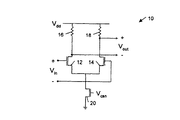
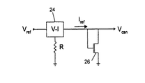
図1を参照すると、従来のCML論理バッファ10は作動対トランジスタ12,14と負荷抵抗16,18とトランジスタ差動対の電源を供給する電流源20からなる。差動対の追加スタックを論理ツリー内に挿入して論理回路を合体させることができる。例えば、図2に示すように、3個の差動対を用いてラッチ22を形成することができる。図3を参照すると、CML電流源用のバイアス電流は通常、基準電流(Iref)をダイオード構成されているNFETカレントミラー26へ供給する主基準電流源24により供給される。主基準電流(Iref)は、定電圧(Vref)源を備えた電圧−電流(V−I)変換器から導出される。定電圧源は、バンドギャップ電圧基準と抵抗(R)から導くことができる。この抵抗は、CMLゲートの負荷抵抗に整合させるか、或いは一定電流が必要な場合は外部の、或いはレーザトリミングを施した精密抵抗とすることができる。
Referring to FIG. 1, a conventional
CML論理セルの速度は、FET差動対スイッチのスイッチング速度だけでなく負荷抵抗におけるRC時定数に依存する。製造過程では、負荷抵抗の値が先ず選択される。次いで、電流源の値がデバイスの大きさにより選択され、負荷抵抗にかかる電圧振幅の許容量が得られる。電圧振幅は通常、次のCML論理ゲートの切り替えに必要とされる電圧に対応する。 速度 The speed of a CML logic cell depends on the RC time constant in the load resistance as well as the switching speed of the FET differential pair switch. In the manufacturing process, the value of the load resistance is first selected. Then, the value of the current source is selected according to the size of the device, and the allowable amount of voltage amplitude applied to the load resistance is obtained. The voltage amplitude typically corresponds to the voltage required for the next CML logic gate switch.
大量生産環境においてCML回路に対するタイミングの要求に応えるため、CMLゲートの速度は、一般に最も遅いFETデバイスに対応する最遅コーナーケースや、ICプロセスで保証される負荷抵抗の公差の最大値、最高温度、そして必要とされる最低Vddに合わせて設計しなければならない。この要件が満たされた状態で、同一の設計を、一般に最速のFETデバイスとICプロセスで保証される負荷抵抗の公差の最小値に対応するワーストケース状況下における最大電力消費量や、最高温度、そして製品が必要とする最高Vddに対して規定し、保証しなければならない。最小限の電力消費はICパッケージのコストを低減し、信頼性を高めることにつながるので、電力消費がより低いということは所与の回路設計の主要な競争に耐える長所となる。現在のところ、CML論理回路系が消費する最大電力は、最遅コーナーケースで必要とされる電流で決まる。 In order to meet the timing requirements for CML circuits in high volume production environments, the speed of the CML gate is generally the slowest corner case corresponding to the slowest FET device, the maximum load resistance tolerance guaranteed by the IC process, the highest temperature. And must be designed for the required minimum Vdd . With this requirement fulfilled, the same design can be used for maximum power consumption under worst-case conditions, generally corresponding to the minimum value of load resistance tolerance guaranteed by the fastest FET device and IC process, maximum temperature, It must be specified and guaranteed for the maximum Vdd required by the product. Lower power consumption has the advantage of withstanding the major competition for a given circuit design, since minimal power consumption leads to lower cost and higher reliability of the IC package. At present, the maximum power consumed by a CML logic system is determined by the current required in the latest corner case.
一つの態様では、本発明は論理回路とバイアス回路を備える回路システムを特徴とするものである。論理回路は、それぞれが個々のテール電流を操作して出力電圧振幅を生成するよう動作可能な1以上の電流モード論理ゲートを含む。バイアス回路は、テール電流レベルの変化によらず各電流モード論理ゲートの電圧振幅を維持するよう動作可能である。 In one aspect, the invention features a circuit system that includes a logic circuit and a bias circuit. The logic circuit includes one or more current mode logic gates each operable to manipulate an individual tail current to produce an output voltage swing. The bias circuit is operable to maintain the voltage swing of each current mode logic gate regardless of changes in the tail current level.
別の態様では、本発明は論理回路とスイッチング速度基準回路を備える回路システムを特徴とするものである。論理回路は、それぞれが個別にテール電流を操作して出力電圧振幅を生成するよう動作可能な1以上の電流モード論理ゲートを含む。スイッチング速度基準回路は、1以上の電流モード論理ゲートの固有スイッチング速度を検出するよう動作可能である。 In another aspect, the invention features a circuit system that includes a logic circuit and a switching speed reference circuit. The logic circuit includes one or more current mode logic gates each individually operable to manipulate the tail current to generate an output voltage swing. The switching speed reference circuit is operable to detect an intrinsic switching speed of one or more current mode logic gates.
別の態様では、本発明は論理回路とテール電流調整回路を備える回路システムを特徴とするものである。論理回路は、それぞれが個々のテール電流を操作して出力電圧振幅を生成せしめるよう動作可能な1以上の電流モード論理ゲートを含む。テール電流調整回路は、電流モード論理ゲートテール電流を動的に調整して基準クロック周波数に相関させて論理ゲートスイッチング速度を維持するよう動作可能である。 In another aspect, the invention features a circuit system that includes a logic circuit and a tail current adjustment circuit. The logic circuit includes one or more current mode logic gates, each operable to manipulate an individual tail current to produce an output voltage swing. The tail current adjustment circuit is operable to dynamically adjust the current mode logic gate tail current to correlate to a reference clock frequency to maintain logic gate switching speed.
本発明の他の特徴及び効果は、図面と特許請求の範囲を含む以下の説明から明らかとなろう。 Other features and advantages of the invention will be apparent from the following description, including the drawings and the claims.
以下の説明では、同様の参照符号は同様の要素を特定するのに用いるものとする。さらに、図面は例示実施形態の主要な特徴を図解することを意図して線図により描いたものである。図面は、実際の実施形態の全ての特徴、或いは図示した要素の相対的な寸法の描写も意図しておらず、実寸で描いたものではない。 In the following description, like reference numerals are used to identify like elements. Moreover, the drawings are diagrammatically illustrated to illustrate key features of the exemplary embodiments. The drawings are not intended to depict all features of the actual embodiments or the relative dimensions of the illustrated elements and are not drawn to scale.
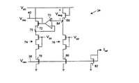
図4を参照すると、一実施形態では、回路システム30は様々な種類の異なる機能のうちの一つとして機能可能な一組の論理ブロック32と、バイアス発生器34と、バイアス電流調整回路36とを含む。例示実施形態では、一組の論理ブロック32は一般的な可調整コモンモード論理(ACML)設計に従ったものとなっている。このACML設計に従って、各ACML論理ブロックは電流源と、調整可能な負荷抵抗を有する負荷と、差動対電流制御回路網(current steering network)を含む。バイアス発生器34は、ACML論理ブロックの電流源に接続される電流源設定出力38と、ACML論理ブロックの負荷に接続される負荷抵抗設定出力40とを有する。バイアス発生器34は、基準電流(Iref)に基づいて所定の電源電流を供給するようにACML電流源を設定可能である。この基準電流(Iref)は、バイアス電流調整回路36から供給される基準電流(Irefa)と、始動電流源42から供給される始動電流(Istart)との組み合わせに対応する。バイアス発生器34はまた、電源電流(の増減)に逆行してACML負荷を設定し、結果として所与の電流源設定(値)に対しロジック信号の振幅レベルをほぼ維持するような負荷抵抗レベルにACML負荷を設定するよう動作可能である。こうして、バイアス発生器34はACML論理に必要とされる電流を調整し、最遅コーナーケースにおけるタイミング要件と、最速コーナーケースにおける電力消費を切り離すことができるようになっている。特に、バイアス発生器34は、ACMLバイアス電流を遅いコーナーケースでは増大させ、速いコーナーケースでは減少させることを可能とするとともに、ACML負荷抵抗レベルを自動調整してロジック信号の必要振幅レベルを維持する。こうして、高速処理が行われるコーナーケースに通常関連する最大電力消費は排除される。これにより、トータルの電力消費の上限が低められ、ICパッケージに必要なコストの低減とより高い信頼性が得られる。
Referring to FIG. 4, in one embodiment, the
図5を参照する。一般に、ACML論理ブロック44は、電流源46と調整可能な負荷48と差動対電流制御回路網50を含む。電流源46は、第1の電圧のレール(例えばグラウンド)に結合され、電源電流(Isource)を供給するよう動作可能である。可調整負荷48は第2の電圧のレール(例えばVdd)に結合してあり、入力された負荷抵抗設定電圧Vcspのレベルに従って調整可能な負荷抵抗を有する。差動対電流制御回路網50は、コンプリメンタリの入力及び出力と、電流源と負荷の間に結合した1以上の差動対を含む。
Please refer to FIG. Generally, ACML
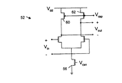
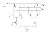
図5に示すACML論理ブロック44は、図6に示すようなバッファ52や、図7に示すようなラッチ54を含む様々な異なる論理回路のうちの任意の一つの形態として機能することができる。これらの機能形態では、ACML電流源はグラウンドに連結したn型電界効果トランジスタ(NFET)56,58である。バイアス発生器34(図4)のソース電流設定出力38がバイアス電圧(Vcsn)を印加し、NEET電流源56,58で供給されるテール電流を設定する。これらの機能形態では、調整可能な負荷はp型電界効果トランジスタ(PFET)60,62,64,66である。バイアス発生器34(図4)の負荷抵抗設定出力40が、PFET負荷60〜66のトライオードバイアス領域にあるバイアス電圧(Vcsp)を印加する。これらの機能形態では、PFET負荷60〜66はバイアス発生器34(図4)により調整可能な抵抗値をもった可変抵抗として機能し、バイアス発生器34により設定することのできる様々なテール電流レベルに対しロジック信号の所要の振幅レベルを維持する。
The ACML
図8を参照すると、いくつかの実施形態では、バイアス発生器34はロジック信号の振幅設定トランジスタ68とオペアンプ70と出力トランジスタ72と一対のレベルシフタ74,76と一対の電流源トランジスタ78,80を含む。基準電流IrefがNFETダイオードカレントミラー82内へ供給され、これによって電源電流設定出力バイアスVcsnが生成される。このバイアスがまた、電流源トランジスタ78,80を駆動する。例示実施形態では、レベルシフタ74と出力トランジスタ72との組み合わせがACML論理回路54(図7)の論理スタックと同様の機能を有し、これにより電流源トランジスタ78の早期効果を補償して電流源トランジスタ58(図7)と緊密に整合させる。特に、出力トランジスタ72がPFET負荷60〜66(図6、図7)と同様の機能を有し、レベルシフタが二つのレベルのACMLスイッチングと同様の機能を有する。レベルシフタ76もまた、二つのレベルのACMLスイッチングと同様の機能を有する。ロジック信号の振幅設定トランジスタ68は、Vddレールとロジック信号振幅設定出力端84との間にダイオードとして接続してある。電流源トランジスタ80により供給される電流に応答してロジック信号振幅設定トランジスタ68の両端にはロジック信号振幅電圧(Vswg)が生じる。ロジック信号振幅設定出力端84に生じた電圧(すなわちVswg)がオペアンプ70の非反転入力端に供給される。オペアンプ70はロジック信号振幅設定出力端84とバイアス発生器34の負荷抵抗設定出力端40との間にフォロワとして結合してあり、オペアンプ70の電圧出力は負荷抵抗設定出力バイアスVcspに対応する。
Referring to FIG. 8, in some embodiments, the
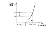
動作時に、電圧Vswgがバイアス電流Irefとは比較的無関係の所望レベルに設定してあるものと先ず仮定する。Irefが増加あるいは減少すると、電流源78とPチャンネルFET72を通る電流は比例的に変化する。オペアンプ70は接続点75における電圧を監視し、Vcspを調整してFET72の抵抗を変化させ、接続点75が接続点84と同電圧となるようにする。負荷トランジスタとしての出力トランジスタ(FET)72は線形トライオード領域で動作し、図9に示すように、ゲート電圧(Vgs)を変化させることでその抵抗値は調整される。
In operation, it is first assumed that voltage V swg is set to a desired level that is relatively independent of bias current I ref . As Iref increases or decreases, the current through
本実施形態では、ロジック信号振幅電圧(Vswg)はNFETトランジスタ68で生成され、何故ならACML論理ブロックが必要とする電圧振幅はNFET差動対を切り替えるのに必要な電圧振幅に対応しているからである。こうして、Vswgは製造工程や温度に起因するスレショールド電位(Vth)の変動に追従する。Vswgの変化は、図10に示す如く、そのドレイン電流の変化に比して比較的小さなものとなる。
In this embodiment, the logic signal swing voltage (V swg ) is generated by
他の実施形態では、Vdd/2或いはバンドギャップ基準電位から得られたもの等、異なるロジック信号振幅レベルを用いることもできる。 In other embodiments, different logic signal amplitude levels may be used, such as those obtained from V dd / 2 or a bandgap reference potential.
図4を再度参照すると、バイアス電流調整回路36は基準クロック周波数frefに相関させて基準電流Irefを調整するよう動作可能である。特に、バイアス電流調整回路36は基準クロック周波数に追従して基準電流を増減するように動作可能であり、従ってACML論理ブロックの電源電流を増減可能で、所望のスイッチング速度を得ることができる。こうして、バイアス電流調整回路36はレール・ツー・レール論理回路系の長所(すなわちより低いクロック速度でのより低い電力消費)を達成し、その一方で電流モード論理回路系の長所(すなわち低減された電流スパイク)を依然として達成する。例示実施形態では、バイアス電流調整回路36はスイッチング速度基準回路84と周波数比較器86と積分器88を含む。スイッチング速度基準回路84はACML論理ブロックと実質的にマッチさせてあり、論理回路(ACML論理ブロック)のスイッチング速度を表わす出力信号frepを生成するよう動作可能としてある。
Referring again to FIG. 4, the bias
図11を参照すると、一実施形態では、スイッチング速度基準回路84は一連のACMLインバータ92で構築したリング発振器90とされる。この構成では、スイッチング速度基準回路84は、バイアス発生器34(図4)と共働して電流制御発振器(ICO)として機能し、ここで発振周波数は基準電流Irefに比例する。リング発振器90は、その意図した動作範囲内で発振停止すべきではない。リング遅延インバータは同じACML系ブロックであるため、ACML論理ブロック32の速度はリング発振器90の速度に追従する。
Referring to FIG. 11, in one embodiment, the switching
再度図4および図12を参照すると、スイッチング速度基準回路84の出力信号frepが周波数比較器86の入力端に供給され、この比較器が出力信号frepと基準クロック信号frefとの間の比較に基づいて出力fcompareを生成するよう動作可能である。いくつかの実施形態では、スイッチング速度基準回路84と周波数比較器86はACML論理ブロックで構成される。図12に示したように、一実施形態では、周波数比較器86は分周器94と周波数検出器96にて実施することができる。分周器94は、スイッチング速度基準回路84の出力信号frepを適当量にて分周する。周波数検出器96は得られた分周信号を基準クロック信号frefと比較し、リング発信器から出力された周波数が基準クロック周波数を超える(アップ)か満たない(ダウン)を示す出力信号fcompareを生成する。周波数検出器96は、回転検出器或いはリセット機能付きストップウオッチを含む様々な周知の周波数検出器のうちの任意の一つで実施することができる。周波数検出器96のアップ/ダウン指示値は、積分器88により積分される。
Referring again to FIGS. 4 and 12, the output signal f rep of the switching
図13を参照すると、一実施形態では、積分器88はチャージポンプ98とコンデンサ100を含む。電圧−電流(V−I)変換器102はチャージポンプ出力端での電圧Vrefaを出力電流Irefaへ変換する。リング発振器の分周周波数が基準クロック周波数に一度整合すると、V−I変換器102に供給された基準電圧は公称値周りで微動させられる。ループは閉じているため、Vcsnバイアス電圧は発振周波数を外部基準クロックfrefにロックした状態に保つよう調整される。周波数変動はチャージポンプ電流と積分コンデンサ値と実効ICO(電流制御発振器)ゲインにより決定される。
Referring to FIG. 13, in one embodiment,
図14を参照すると、別の実施形態では、積分器88はディジタル/アナログ変換器(DA変換器)106を駆動するアップ/ダウンカウンタ104で実施される。DA変換器106は、Vrefaバイアス信号を駆動する。Vrefa精度の分解能は、DA変換器106の分解能に基づく。この実施形態では、図13の積分器実施形態のアナログ機能がディジタル機能に置き換えてある。
Referring to FIG. 14, in another embodiment,
一部実施形態では、図13,14の積分器実施形態のV−I変換器102は取り除かれ、Vrefa出力端は直接Vcsnへ接続するものであってもよい。
In some embodiments, the
図4を参照すると、電力増強時には、スイッチング速度基準回路84や周波数比較器86などの図示の回路システム30内の少なくとも一部のACML論理セルは、バイアス電圧Vcsnが適正に漸増するよう機能させねばならない。図示の実施形態では、電流源42はスタートアップトリックル(少しずつ流す)電流Istartを供給し、スイッチング速度基準回路84と周波数比較器86用のACML論理回路の機能を保証する。別の実施形態では、周波数比較器86は定電流源に接続した個別の独立したバイアス発生器によりバイアスされる。さらに別の実施形態では、周波数比較器86はバイアスを一切必要としない従来のレール・ツー・レールCMOS論理回路をもって実施される。この実施形態では、ACMLレベルをCMOS論理回路のレベルへ整合させるのに論理レベル変換器が必要となることがある。
Referring to FIG. 4, during power augmentation, at least some of the ACML logic cells in the illustrated
他の実施形態は特許請求の範囲内にある。 Other embodiments are within the claims.
例えば、上記の実施形態は電界効果トランジスタ回路に関連して説明したが、これらの実施形態はバイポーラトランジスタ技術などの他のトランジスタ技術をもって実施することもできる。 For example, while the above embodiments have been described with reference to field effect transistor circuits, these embodiments may be implemented with other transistor technologies, such as bipolar transistor technology.
なお、本発明は例として以下の態様を含む。
[1] 個々のテール電流を操作して出力電圧振幅を生成するようそれぞれが動作可能な1以上の電流モード論理ゲートを備える論理回路(44)と、
テール電流レベルにおける変化によらず、各電流源モード論理ゲートの電圧振幅を維持するよう動作可能なバイアス回路(34)と、
を備えることを特徴とする回路システム(30)。
[2] 前記論理回路(44)が、
第1の電圧のレールに結合され、電源電流を供給するよう動作可能な電流源(46)と、
第2の電圧のレールに結合され、調整可能な負荷抵抗を有する負荷(48)と、
前記電流源(46)と前記負荷(48)の間に接続され、コンプリメンタリ入力及び出力を有する差動対電流制御回路網(50)とを備え、
前記バイアス回路(34)は、前記電流源(46)に接続された電源電流設定出力と前記負荷(48)に結合した負荷抵抗設定出力とを有しており、
前記バイアス回路(34)は、所与の電源電流を供給するよう前記電流源(46)を設定し、また、電源電流源に逆行して前記負荷(48)を設定し、結果として所与の電源電流設定に対して前記論理回路(44)の前記コンプリメンタリ出力間のロジック信号振幅レベルをほぼ維持するように前記負荷(48)を設定するよう動作可能である、
ことを特徴とする[1]に記載の回路システム。
[3] 前記負荷(48)が、前記バイアス回路(34)の前記負荷抵抗設定出力に接続される制御入力をそれぞれ有する一対のトランジスタを備える、
ことを特徴とする[2]に記載の回路システム。
[4] 前記バイアス回路(34)が、ロジック信号振幅設定トランジスタ(68)を備える、
ことを特徴とする[2]に記載の回路システム。
[5] 前記バイアス回路(34)は、前記電流源(46)を設定して入力した基準電流に基づく所与の電源電流を供給するよう動作可能であり、さらに、前記バイアス回路(34)に接続され、基準クロック周波数に相関して前記基準電流を調整するよう動作可能なバイアス電流調整回路(36)を備える、
ことを特徴とする[2]に記載の回路システム。
[6] 前記バイアス電流調整回路(36)は、前記論理回路(44)とほぼマッチさせてあって論理回路スイッチング速度を表わす出力信号を生成するよう動作可能なスイッチング速度基準回路(84)を備える、
ことを特徴とする[5]に記載の回路システム。
[7] 前記スイッチング速度基準回路(36)がリング発振器(90)を備える、
ことを特徴とする[6]に記載の回路システム。
[8] 前記スイッチング速度基準回路(36)からの前記出力信号と基準周波数信号との比較に基づいて出力を生成するよう動作可能な周波数比較器(86)を備える、
ことを特徴とする[6]に記載の回路システム。
[9] 個々のテール電流を制御して出力電圧振幅を生成するようそれぞれが動作可能な1以上の電流モード論理ゲートを有する論理回路(44)と、前記1以上の電流モード論理ゲートの固有スイッチング速度を検出するよう動作可能なスイッチング速度基準回路(84)とを備える、
ことを特徴とする回路システム(30)。
[10] 個々のテール電流を制御して出力電圧振幅を発生させるようそれぞれが動作可能な1以上の電流モード論理ゲートを有する論理回路(44)と、
前記電流モード論理ゲートのテール電流を動的に調整し、基準クロック周波数に相関させて論理ゲートスイッチング速度を維持するよう動作可能なテール電流調整回路(36)とを備える、
ことを特徴とする回路システム(30)。
The present invention includes the following aspects as examples.
[1] A logic circuit (44) comprising one or more current mode logic gates each operable to manipulate an individual tail current to produce an output voltage swing;
A bias circuit (34) operable to maintain the voltage swing of each current source mode logic gate regardless of changes in tail current levels;
A circuit system (30), comprising:
[2] The logic circuit (44)
A current source (46) coupled to the first voltage rail and operable to supply a power supply current;
A load (48) coupled to the rail of the second voltage and having an adjustable load resistance;
A differential pair current control network (50) connected between the current source (46) and the load (48) and having complementary inputs and outputs;
The bias circuit (34) has a power supply current setting output connected to the current source (46) and a load resistance setting output coupled to the load (48);
The bias circuit (34) sets the current source (46) to supply a given power supply current, and sets the load (48) counter to the power supply current source, resulting in a given power supply current. Operable to set the load (48) to substantially maintain a logic signal amplitude level between the complementary outputs of the logic circuit (44) with respect to a power supply current setting;
The circuit system according to [1], wherein:
[3] The load (48) includes a pair of transistors each having a control input connected to the load resistance setting output of the bias circuit (34).
The circuit system according to [2], wherein:
[4] The bias circuit (34) includes a logic signal amplitude setting transistor (68).
The circuit system according to [2], wherein:
[5] The bias circuit (34) is operable to set the current source (46) to supply a given power supply current based on the input reference current, and further to the bias circuit (34). A bias current adjustment circuit (36) connected and operable to adjust the reference current relative to a reference clock frequency;
The circuit system according to [2], wherein:
[6] The bias current adjusting circuit (36) includes a switching speed reference circuit (84) substantially matched with the logic circuit (44) and operable to generate an output signal representing a logic circuit switching speed. ,
The circuit system according to [5], wherein:
[7] The switching speed reference circuit (36) includes a ring oscillator (90).
The circuit system according to [6], wherein:
[8] a frequency comparator (86) operable to generate an output based on a comparison between the output signal from the switching speed reference circuit (36) and a reference frequency signal;
The circuit system according to [6], wherein:
[9] A logic circuit (44) having one or more current mode logic gates each operable to control an individual tail current to generate an output voltage swing, and inherent switching of said one or more current mode logic gates. A switching speed reference circuit (84) operable to detect speed.
A circuit system (30), characterized in that:
[10] A logic circuit (44) having one or more current mode logic gates each operable to control an individual tail current to generate an output voltage swing;
A tail current adjustment circuit (36) operable to dynamically adjust a tail current of the current mode logic gate and correlate to a reference clock frequency to maintain logic gate switching speed.
A circuit system (30), characterized in that:
10 CML論理バッファ
12,14 トランジスタ差動対
16,18 負荷抵抗
20 電流源
22 ラッチ
24 主基準電流源
26 ダイオード構成NFET電流ミラー
30 回路システム
32 論理ブロック
34 バイアス発生器(バイアス回路)
36 バイアス電流調整回路
38 電流源設定出力端
40 負荷抵抗設定出力端
42 始動電流源
44 ACML論理ブロック(論理回路)
46 電流源
48 可調整負荷
50 差動対電流操作回路網
52 バッファ
54 ラッチ
56,58 NEET電流源
60,62,64,66 p型電界効果トランジスタ(PFET)
68 ロジック信号振幅設定トランジスタ
70 オペアンプ
72 出力トランジスタ
74,76 レベルシフタ
78,80 一対の電流源トランジスタ
82 NFETダイオード電流ミラー
84 ロジック信号振幅設定出力端
84 スイッチング速度基準回路
86 周波数比較器
88 積分器
90 リング発振器
94 分周器
96 周波数検出器
98 チャージポンプ
100 コンデンサ
102 電圧−電流(V−I)変換器
104 アップ/ダウンカウンタ
106 ディジタル/アナログ変換器(DA変換器)
36 Bias
46
68 Logic signal
Claims (1)
テール電流レベルにおける変化によらず、各電流源モード論理ゲートの電圧振幅を維持するよう動作可能なバイアス回路と、
を備えることを特徴とする回路システム。
A logic circuit comprising one or more current mode logic gates each operable to manipulate an individual tail current to produce an output voltage swing;
A bias circuit operable to maintain the voltage swing of each current source mode logic gate regardless of changes in tail current levels;
A circuit system comprising:
Applications Claiming Priority (1)
| Application Number | Priority Date | Filing Date | Title |
|---|---|---|---|
| US10/233,715 US6762624B2 (en) | 2002-09-03 | 2002-09-03 | Current mode logic family with bias current compensation |
Publications (2)
| Publication Number | Publication Date |
|---|---|
| JP2004096750A true JP2004096750A (en) | 2004-03-25 |
| JP2004096750A5 JP2004096750A5 (en) | 2007-01-25 |
Family
ID=28791680
Family Applications (1)
| Application Number | Title | Priority Date | Filing Date |
|---|---|---|---|
| JP2003299973A Withdrawn JP2004096750A (en) | 2002-09-03 | 2003-08-25 | Current mode logic circuit system having bias current compensation |
Country Status (3)
| Country | Link |
|---|---|
| US (1) | US6762624B2 (en) |
| JP (1) | JP2004096750A (en) |
| GB (2) | GB2419050B (en) |
Cited By (5)
| Publication number | Priority date | Publication date | Assignee | Title |
|---|---|---|---|---|
| JP2007324799A (en) * | 2006-05-31 | 2007-12-13 | Nec Electronics Corp | Output circuit and semiconductor integrated circuit device |
| US7429874B2 (en) | 2005-11-15 | 2008-09-30 | Electronics And Telecommunications Research Institute | Replica bias circuit |
| US7759992B2 (en) | 2006-03-30 | 2010-07-20 | Nec Corporation | CML circuit and clock distribution circuit |
| JP2015065687A (en) * | 2014-11-26 | 2015-04-09 | 富士通株式会社 | Signal shaping circuit |
| WO2016199522A1 (en) * | 2015-06-12 | 2016-12-15 | ザインエレクトロニクス株式会社 | Signal transmission circuit and oscillation circuit |
Families Citing this family (30)
| Publication number | Priority date | Publication date | Assignee | Title |
|---|---|---|---|---|
| US6946918B2 (en) * | 2002-01-16 | 2005-09-20 | Oki Electric Industry Co., Ltd. | Differential voltage to current converter having transistors of different sizes |
| US7355451B2 (en) * | 2004-07-23 | 2008-04-08 | Agere Systems Inc. | Common-mode shifting circuit for CML buffers |
| US7626422B2 (en) * | 2004-10-08 | 2009-12-01 | Samsung Electronics Co., Ltd. | Output driver and method thereof |
| US7187212B1 (en) * | 2004-10-26 | 2007-03-06 | National Semiconductor Corporation | System and method for providing a fast turn on bias circuit for current mode logic transmitters |
| US7268623B2 (en) * | 2004-12-10 | 2007-09-11 | Electronics And Telecommunications Research Institute | Low voltage differential signal driver circuit and method for controlling the same |
| US7417574B2 (en) * | 2004-12-13 | 2008-08-26 | Texas Instruments Incorporated | Efficient amplifier sharing in a multi-stage analog to digital converter |
| US7750693B2 (en) * | 2007-06-05 | 2010-07-06 | O2Micro, Inc. | Frequency divider including latch circuits |
| JP4384207B2 (en) * | 2007-06-29 | 2009-12-16 | 株式会社東芝 | Semiconductor integrated circuit |
| US20090054004A1 (en) * | 2007-08-20 | 2009-02-26 | Zerog Wireless, Inc., Delaware Corporation | Biasing for Stacked Circuit Configurations |
| JP2009251573A (en) * | 2008-04-11 | 2009-10-29 | Hitachi Displays Ltd | Display |
| US8339176B2 (en) * | 2008-05-30 | 2012-12-25 | Infineon Technologies Ag | System and method for providing a low-power self-adjusting reference current for floating supply stages |
| US7915950B2 (en) * | 2008-06-20 | 2011-03-29 | Conexant Systems, Inc. | Method and algorithm of high precision on-chip global biasing using integrated resistor calibration circuits |
| US7679420B1 (en) * | 2008-08-28 | 2010-03-16 | Micrel, Incorporated | Slew rate controlled level shifter with reduced quiescent current |
| US7961057B2 (en) * | 2008-08-28 | 2011-06-14 | Mediatek Singapore Pte Ltd | Voltage controlled oscillator |
| TW201037529A (en) | 2009-03-02 | 2010-10-16 | David Reynolds | Belief propagation processor |
| US8115513B2 (en) * | 2009-03-02 | 2012-02-14 | Mitsubishi Electric Research Laboratories, Inc. | Circuits for soft logical functions |
| US8633732B2 (en) * | 2009-03-02 | 2014-01-21 | Mitsubishi Electric Research Laboratories, Inc. | Circuits for soft logical functions |
| US8458114B2 (en) * | 2009-03-02 | 2013-06-04 | Analog Devices, Inc. | Analog computation using numerical representations with uncertainty |
| GB2473181B (en) * | 2009-07-24 | 2016-07-13 | Texas Instruments Ltd | Improved cml to cmos converter |
| US8972831B2 (en) | 2010-01-11 | 2015-03-03 | Analog Devices, Inc. | Belief propagation processor |
| US9047153B2 (en) | 2010-02-22 | 2015-06-02 | Analog Devices, Inc. | Selective delay of data receipt in stochastic computation |
| WO2011103565A1 (en) | 2010-02-22 | 2011-08-25 | Lyric Semiconductor, Inc. | Mixed signal stochastic belief propagation |
| TWI491180B (en) * | 2010-09-08 | 2015-07-01 | Mstar Semiconductor Inc | Low voltage transmitter with high output voltage |
| CN102402239B (en) * | 2010-09-15 | 2014-02-19 | 晨星软件研发(深圳)有限公司 | Low-voltage transmission device with high-output voltage |
| KR101183628B1 (en) * | 2010-12-09 | 2012-09-18 | 에스케이하이닉스 주식회사 | Semiconductor device and operating methode for the same |
| US8847628B1 (en) * | 2012-09-29 | 2014-09-30 | Integrated Device Technology Inc. | Current mode logic circuits with automatic sink current adjustment |
| US8760190B1 (en) | 2012-12-05 | 2014-06-24 | Lsi Corporation | External component-less PVT compensation scheme for IO buffers |
| US9401643B1 (en) * | 2015-03-10 | 2016-07-26 | International Business Machines Corporation | Bias-temperature induced damage mitigation circuit |
| US9319041B1 (en) * | 2015-04-08 | 2016-04-19 | Global Unichip Corporation | Squelch detector |
| CN107370463B (en) * | 2017-06-15 | 2023-09-01 | 西安华泰半导体科技有限公司 | Offset self-correction operational amplifier based on back gate effect and channel length modulation effect |
Family Cites Families (15)
| Publication number | Priority date | Publication date | Assignee | Title |
|---|---|---|---|---|
| US4145623A (en) | 1977-10-04 | 1979-03-20 | Burroughs Corporation | Current mode logic compatible emitter function type logic family |
| US5197033A (en) * | 1986-07-18 | 1993-03-23 | Hitachi, Ltd. | Semiconductor device incorporating internal power supply for compensating for deviation in operating condition and fabrication process conditions |
| US5041747A (en) * | 1986-07-23 | 1991-08-20 | Tandem Computers Incorporated | Delay regulation circuit |
| US5065055A (en) * | 1990-12-20 | 1991-11-12 | Sun Microsystems, Inc. | Method and apparatus for high-speed bi-CMOS differential amplifier with controlled output voltage swing |
| US5124580A (en) * | 1991-04-30 | 1992-06-23 | Microunity Systems Engineering, Inc. | BiCMOS logic gate having linearly operated load FETs |
| JP3288727B2 (en) * | 1991-05-24 | 2002-06-04 | 株式会社東芝 | Output circuit |
| DE4337511A1 (en) * | 1993-11-03 | 1995-05-04 | Siemens Ag | Inverter stage |
| WO1996010865A1 (en) * | 1994-10-03 | 1996-04-11 | Motorola Inc. | Method and apparatus for providing a low voltage level shift |
| JP3557275B2 (en) * | 1995-03-29 | 2004-08-25 | 株式会社ルネサステクノロジ | Semiconductor integrated circuit device and microcomputer |
| US5684429A (en) * | 1995-09-14 | 1997-11-04 | Ncr Corporation | CMOS gigabit serial link differential transmitter and receiver |
| US5909127A (en) * | 1995-12-22 | 1999-06-01 | International Business Machines Corporation | Circuits with dynamically biased active loads |
| GB9707349D0 (en) | 1997-04-11 | 1997-05-28 | Univ Waterloo | A dynamic current mode logic family |
| US5889431A (en) * | 1997-06-26 | 1999-03-30 | The Aerospace Corporation | Current mode transistor circuit method |
| US5973526A (en) * | 1997-12-19 | 1999-10-26 | Intel Corporation | Compensating a characteristic of a circuit |
| US6094074A (en) * | 1998-07-16 | 2000-07-25 | Seiko Epson Corporation | High speed common mode logic circuit |
-
2002
- 2002-09-03 US US10/233,715 patent/US6762624B2/en not_active Expired - Lifetime
-
2003
- 2003-08-25 JP JP2003299973A patent/JP2004096750A/en not_active Withdrawn
- 2003-08-27 GB GB0526002A patent/GB2419050B/en not_active Expired - Fee Related
- 2003-08-27 GB GB0320078A patent/GB2393596B/en not_active Expired - Fee Related
Cited By (5)
| Publication number | Priority date | Publication date | Assignee | Title |
|---|---|---|---|---|
| US7429874B2 (en) | 2005-11-15 | 2008-09-30 | Electronics And Telecommunications Research Institute | Replica bias circuit |
| US7759992B2 (en) | 2006-03-30 | 2010-07-20 | Nec Corporation | CML circuit and clock distribution circuit |
| JP2007324799A (en) * | 2006-05-31 | 2007-12-13 | Nec Electronics Corp | Output circuit and semiconductor integrated circuit device |
| JP2015065687A (en) * | 2014-11-26 | 2015-04-09 | 富士通株式会社 | Signal shaping circuit |
| WO2016199522A1 (en) * | 2015-06-12 | 2016-12-15 | ザインエレクトロニクス株式会社 | Signal transmission circuit and oscillation circuit |
Also Published As
| Publication number | Publication date |
|---|---|
| GB0526002D0 (en) | 2006-02-01 |
| GB2419050A (en) | 2006-04-12 |
| US6762624B2 (en) | 2004-07-13 |
| US20040041593A1 (en) | 2004-03-04 |
| GB2419050B (en) | 2006-07-26 |
| GB2393596B (en) | 2006-07-26 |
| GB2393596A (en) | 2004-03-31 |
| GB0320078D0 (en) | 2003-10-01 |
Similar Documents
| Publication | Publication Date | Title |
|---|---|---|
| JP2004096750A (en) | Current mode logic circuit system having bias current compensation | |
| US8115559B2 (en) | Oscillator for providing a constant oscillation signal, and a signal processing device including the oscillator | |
| US5847586A (en) | Enhanced power-on-reset/low voltage detection circuit | |
| US6759875B2 (en) | Voltage controlled oscillation circuit | |
| US6466078B1 (en) | Reduced static phase error CMOS PLL charge pump | |
| US7789558B2 (en) | Thermal sensing circuit using bandgap voltage reference generators without trimming circuitry | |
| US5072197A (en) | Ring oscillator circuit having improved frequency stability with respect to temperature, supply voltage, and semiconductor process variations | |
| US7830200B2 (en) | High voltage tolerant bias circuit with low voltage transistors | |
| US20050264336A1 (en) | Differential type delay cells and methods of operating the same | |
| US7812652B2 (en) | Locked loops, bias generators, charge pumps and methods for generating control voltages | |
| CN109845110B (en) | Compensating device for compensating PVT variations of analog and/or digital circuits | |
| US6806692B2 (en) | Voltage down converter | |
| US6177831B1 (en) | Semiconductor integrated circuit with well potential control circuit | |
| US20050068076A1 (en) | Current mirror compensation circuit and method | |
| JPH08223018A (en) | Semiconductor integrated circuit applying variation compensation technique | |
| EP0121793B1 (en) | Cmos circuits with parameter adapted voltage regulator | |
| US11630161B1 (en) | Flexible circuit for droop detection | |
| US5744990A (en) | Enhanced power-on-reset/low voltage detection circuit | |
| US6686788B2 (en) | Delay circuit of clock synchronization device using delay cells having wide delay range | |
| US7385437B2 (en) | Digitally tunable high-current current reference with high PSRR | |
| US20060170477A1 (en) | Semiconductor integrated circuit having output circuit | |
| KR100520269B1 (en) | Voltage-current converter and self-oscillator using the same | |
| US11961569B2 (en) | Clock-generating circuit | |
| US20050110583A1 (en) | Reference voltage generator for logic elements providing stable and predefined gate propagation time | |
| US20210184671A1 (en) | Threshold tracking power-on-reset circuit |
Legal Events
| Date | Code | Title | Description |
|---|---|---|---|
| A711 | Notification of change in applicant |
Free format text: JAPANESE INTERMEDIATE CODE: A711 Effective date: 20060629 |
|
| A521 | Request for written amendment filed |
Free format text: JAPANESE INTERMEDIATE CODE: A523 Effective date: 20060815 |
|
| A621 | Written request for application examination |
Free format text: JAPANESE INTERMEDIATE CODE: A621 Effective date: 20060815 |
|
| RD03 | Notification of appointment of power of attorney |
Free format text: JAPANESE INTERMEDIATE CODE: A7423 Effective date: 20060815 |
|
| A521 | Request for written amendment filed |
Free format text: JAPANESE INTERMEDIATE CODE: A523 Effective date: 20061130 |
|
| A761 | Written withdrawal of application |
Free format text: JAPANESE INTERMEDIATE CODE: A761 Effective date: 20070501 |