JP2004046292A - IC card reader / writer device - Google Patents
IC card reader / writer device Download PDFInfo
- Publication number
- JP2004046292A JP2004046292A JP2002199012A JP2002199012A JP2004046292A JP 2004046292 A JP2004046292 A JP 2004046292A JP 2002199012 A JP2002199012 A JP 2002199012A JP 2002199012 A JP2002199012 A JP 2002199012A JP 2004046292 A JP2004046292 A JP 2004046292A
- Authority
- JP
- Japan
- Prior art keywords
- current
- reader
- card
- writer terminal
- writer
- Prior art date
- Legal status (The legal status is an assumption and is not a legal conclusion. Google has not performed a legal analysis and makes no representation as to the accuracy of the status listed.)
- Pending
Links
Images

Landscapes
- Credit Cards Or The Like (AREA)
- Near-Field Transmission Systems (AREA)
Abstract
【課題】本発明は、規定された最大電流値に対する電流マージンがないとき、負荷状態の変化で電源電流が増大した結果、動作不能となることを防止した非接触型ICカードのリーダライタ端末を提供する。
【解決手段】リーダライタ端末2には、外部装置からUSBケーブル3を介して電源が供給される。該電源の電流を監視する電流監視回路6をUSBケーブルコネクタ5の近傍に配置し、検出電流値が所定値を超えたとき、デジタル処理部7が、ICカードに電力を供給するアンテナA1に出力電流を出力する増幅器の増幅度を変更し、検出電流値に応じて前記出力電流を小さく制御する。
【選択図】 図1An object of the present invention is to provide a non-contact type IC card reader / writer terminal which prevents inoperability as a result of an increase in power supply current due to a change in load state when there is no current margin for a specified maximum current value. provide.
Power is supplied to a reader / writer terminal (2) from an external device via a USB cable (3). A current monitoring circuit 6 for monitoring the current of the power supply is arranged near the USB cable connector 5, and when the detected current value exceeds a predetermined value, the digital processing unit 7 outputs the current to the antenna A1 that supplies power to the IC card. The amplification degree of the amplifier that outputs the current is changed, and the output current is controlled to be small according to the detected current value.
[Selection diagram] Fig. 1
Description
【0001】
【発明の属する技術分野】
本発明は、非接触型ICカードと通信を行うICカードリーダライタ装置に関し、特に、規定された最大電流値に対する電流マージンを確保できないときに、消費電力が増大した結果、動作不能となることを防止した非接触型ICカードと通信を行うICカードリーダライタ装置に関する。
【0002】
【従来の技術】
近年、スマートカードに代表されるように、カードにICチップを埋め込んだICカードを作成し、電子財布を実現させようとしている。また、このICカードを交通手段の定期券や乗車券とすることも行われている。更には、ICタグとしても使用されている。これらのように、カードに内蔵させたICによって種々の機能を実現させることが行われている。
【0003】
これらの機能をICカードで実現するには、通常、このICカードと非接触で無線通信を行うリーダライタ端末を必要とする。そして、非接触型ICカードには、形状的にICを駆動する電源を組み込むことが難しいため、多くは、ICカードから離れた位置にあるリーダライタ端末から送出される無線搬送波を使用して、ICカードのCPUに電力供給するようになっている。
【0004】
一方、リーダライタ端末の駆動電源は、端末が携帯型に構成されている場合には、内蔵されたバッテリから供給されるようになっているが、リーダライタ端末をアップストリーム側のパソコン(PC)或いはホストに接続して利用する場合には、アップストリーム側とリーダライタ端末とはユニバーサル・シリアルバス(USB)で接続されることが多く、この場合には、リーダライタ端末の駆動電力は、USBケーブルを介してアップストリーム側から供給される。
【0005】
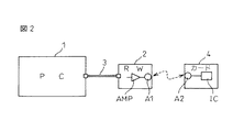
そこで、上述したようなICカードを、リーダライタ端末と非接触で通信させる場合について、その概略構成を図2に示した。
【0006】
リーダライタ端末2は、パソコン1とUSBケーブル3によって接続され、非接触型ICカード4が、リーダライタ(RW)端末2に近づけられたときに、無線で近距離通信が行われる。
【0007】
このリーダライタ端末2には、非接触型のICカード4と無線通信を行うためのRWアンテナA1が備えられ、アンテナA1には、電力増幅する出力アンプAMPが接続され、ICカード4と通信を行うために必要な電力と通信信号を供給する。そして、ICカード4には、アンテナA1と送受信するためのアンテナA2が備えられ、アンテナA2は、ICカード4内のICに電力を受信するとともに、通信信号の送受信を行う。
【0008】
リーダライタ端末2に備えられたRWアンテナA1は、通常、複数回巻かれたループアンテナで構成される。このループアンテナのコイルは、例えば、プリント配線基板上に、複数の線を束ねて平面的に固定されているか、或いは、線自体がプリント配線されてループアンテナを形成している。さらには、プリント配線基板とは別に、リーダライタ端末のRWアンテナA1として、単体で形成されている場合ある。
【0009】
一方、ICカード4に内蔵されたアンテナA2も、アンテナA1と電磁結合するループアンテナで構成される。アンテナA2の出力端には、抵抗、コンデンサ等からなる同調回路が接続されており、リーダライタ端末2内の電力増幅器AMPから供給される搬送波がアンテナA1によって空中線として放射されると、ICカード4のアンテナA2がこの搬送波を受信することによって、ICを駆動するための電力が供給されるとともに、搬送波に重畳された通信信号が受信される。
【0010】
アンテナA1とアンテナA2との通信距離は、それらの電磁誘導作用により、両アンテナが近づけば、アンテナA1の消費電力は、大きくなり、また、反対に、両アンテナが遠ざかれば、その消費電力は、小さくなる。
【0011】
パソコン1とリーダライタ端末2とは、USBケーブル3によって接続される。該USBケーブル3は、パソコン1とリーダライタ端末2とに各々備えられたUSBケーブルコネクタに差し込まれて接続される。このUSBケーブルコネクタに関しては、上流側のコネクタをシリーズAと、下流側のコネクタをシリーズBと称しており、USBケーブル3の端のシリーズAプラグを、上流側のハブであるパソコン1のシリーズAソケットに差し込まれる。そして、USBケーブル3の他端のシリーズBプラグをリーダライタ端末のシリーズBソケットに差し込まれる。
【0012】
【発明が解決しようとする課題】
この様に、パソコン1とリーダライタ端末2とは、USBケーブル3を介して接続されるが、USBは、シリアルデータを差動信号として伝送するものであり、そのUSBケーブルは、一対の信号線(D+、D−)と一対の電源線(Vbus、GND)の4本のケーブルで構成されている。この一対の電源線によって、リーダライタ端末2の駆動用の電力がパソコン1から供給される。しかし、従来のリーダライタ端末2では、このUSBケーブルの電源線に流れる電流を監視していなかった。
【0013】
USBケーブル3の電源線からリーダライタ端末2へ電力を供給する場合、USBの規定から最大値は、5V、500mAとなっている。実際のリーダライタ端末では、この規定値の範囲内ではあるが、最大値に近いギリギリの値で動作するように設計される場合がある。これは、非接触型のICカードリーダライタ端末2では、アンテナA1から供給される電力が大きいほど、ICカード4との通信距離を延ばすことができるという事情に拠っており、定めた目標距離で通信を行わせるようにした結果、電流マージンをあまり大きく確保することができないことがある。
【0014】
この様なリーダライタ端末が動作している最中に、例えば、ICカード4の扱われ方によっては、アンテナA1とアンテナA2との電磁誘導作用の結果、アンテナA1からの送信電力が大きくなってしまう場合がある。このようなとき、電流マージンが少ないため、USBケーブル3の電源線を流れる電流値が規定された最大値を超えたものとなり得る。
【0015】
そこで、このような状態になると、アップストリーム側のホスト(又はハブ)であるパソコン1が、USBケーブル3による電力供給を中止することになっており、リーダライタ端末2の再初期化を行うようになっている。そのため、この作業の間、リーダライタ端末2は、動作不能状態となってしまう。
【0016】
リーダライタ端末2がICカード4へアクセスしている最中に、リーダライタ端末4が動作不能状態に陥った場合には、ICカード4内に保存されているデータ内容が保証できない等の不具合が生じる可能性があり、この様なことは、ICカード利用上、問題となるために、何らかの対策を講じる必要がある。
【0017】
また、リーダライタ端末に内蔵したバッテリ等によってリーダライタ端末への電力供給を行う場合でも、やはり、該バッテリの最大供給能力を超えると、リーダライタ端末は、動作不能状態とされ、この場合でも、同様に、ICカード利用上、問題となるために、何らかの対策を講じる必要がある。
【0018】
そこで、本発明は、非接触型ICカードと通信を行うものであって、規定された最大電流値に対する電流マージンが大きくないときに、負荷状態が変化して電源電流が増大した結果、動作不能となることを防止したICカードリーダライタ装置を提供することを目的とする。
【0019】
【課題を解決するための手段】
以上の課題を解決するため、本発明によるICカードリーダライタ装置には、該電源の電流を監視する電流監視回路と、ICカードに電力を供給するアンテナに出力電流を出力する増幅器と、前記電流監視回路の検出電流値に応じて前記出力電流を制御する制御部とが備えられ、前記制御部は、前記検出電流値が所定値を超えたとき、前記出力電流を小さく制御することを特徴としている。
【0020】
そして、前記電源は、外部装置からUSBケーブルを介して供給され、前記電流監視回路は、前記USBケーブルソケットの近傍に配置されることとした。
【0021】
さらに、前記制御部は、前記増幅器の増幅度を制御し、或いは、前記検出電流値の大きさに応じて、前記増幅度を多段階に制御するようにした。
【0022】
また、前記制御部は、前記出力電流を小さく制御した場合に、所定時間経過後に前記出力電流を前の大きさに制御することとし、前記制御部は、前記出力電流を小さく制御したとき、利用者に報知するようにした。
【0023】
【発明の実施の形態】
次に、本発明のICカードリーダライタ装置の実施形態について、図1を参照しながら説明する。図1では、本実施形態として、ICカードと非接触で通信するリーダライタ端末が、パソコンにUSBケーブルで接続されている場合を実施例として挙げている。
【0024】
本実施形態では、電源の電力供給能力を超えた出力電流が流れたとき、リーダライタ端末が動作不能に陥ることを防止する対策として、リーダライタ端末に備えられたアンテナの負荷状態に応じて変化する電源線の電流を監視し、該電流が所定電流値を超えたとき、アンテナへの出力電流を抑制する制御方式とした。
【0025】
図1には、ICカードと非接触で通信するリーダライタ端末における回路構成が示されている。なお、リーダライタ端末の全体回路構成は、従来のものが使用されるので、図1では、省略されており、リーダライタ端末の電源供給部とアンテナへの出力電流供給部分について、本実施形態に関連する回路構成を示した。
【0026】
リーダライタ端末2には、USBによりパソコン1と送受信するために、USBケーブルコネクタ5が設けられている。このUSBケーブルコネクタ5において、リーダライタ端末側のシリーズBソケットに、USBケーブル3のシリーズBプラグが差し込まれている。リーダライタ端末2の駆動電源は、USBケーブル3の一対の電源線Vbus、GNDから、USBケーブルコネクタ5を介して供給される。
【0027】
そこで、本実施形態では、リーダライタ端末2の内部において、USBケーブルコネクタ5の近傍の電源線上に、電流監視回路6を設置した。この電流監視回路6は、電源線を流れる電流の大きさを監視し、任意に設定した電流検出値Ithに対し、電源線を流れる電流値Iがこの電流検出値Ithを超えた場合に、検出信号Sを出力するように動作する。この設定される電流検出値Ithは、例えば、最大供給値から若干のマージンが考慮され、例えば、規定値が500mAであれば、450mAのような値とされる。
【0028】
電流監視回路6は、電源線を流れる電流値Iがこの電流検出値Ithを超えたとき、検出信号Sをデジタル処理部(CPU)7へ送出する。検出信号Sを受け取ったデジタル処理部7は、検出信号Sに基づいてRF出力部の出力電流を制御する。なお、デジタル処理部7は、電源線の電流監視のためだけのCPUであっても、又は、リーダライタ端末2の全体を制御するCPUであってもよい。
【0029】
アンテナA1に電力を供給するRF出力部の回路構成は、出力アンプAMPを基本とし、出力アンプAMPは、リーダライタ端末2内の変調部で生成された通信信号をアンテナA1に出力する役割を有している。出力アンプAMPには、抵抗値を可変とする帰還抵抗が接続されている。この帰還抵抗の値を変更して出力アンプAMPの増幅度を変更している。
【0030】
図1に示されるように、出力アンプAMPの帰還抵抗は、抵抗R1及びR2が並列に接続されており、一方の抵抗、図では、抵抗R1と直列にスイッチSWが挿入されている。このスイッチSWのオン・オフにより、帰還抵抗の大きさが変わり、出力アンプAMPの増幅度が変更される。
【0031】
デジタル処理部7は、電流監視回路6から検出信号Sを受信したとき、スイッチSWをオンに制御し、RF出力部の出力アンプAMPに接続されている抵抗R1を帰還抵抗に追加する。この制御により、出力アンプAMPの増幅度が小さくされ、アンテナ部のアンテナA1への出力電流を抑制することができる。
【0032】
ここで、アンテナ部のアンテナA1への出力電流が抑制されるということは、ICカードに備えられたアンテナA2とアンテナA1との通信距離が、アンテナの消費電力に応じて、出力電流抑制前より短くなることを意味する。例えば、通信距離10cmとしていたものが、5cmと短くなる。この様に、リーダライタ端末2とICカード4との通信距離が狭まってしまう結果になるが、リーダライタ端末自体の動作不能という事態を確実に回避することができる。出力電流が抑制されたときには、ICカードの利用者は、当該ICカードをリーダライタ端末2のアンテナA1にさらに近づけることによって、通信処理を実行させることができる。
【0033】
このとき、リーダライタ端末2側で、電源線に流れる電流が監視され、その大きさによってアンテナA1の出力が自動的に抑制されることになるので、ICカードの利用者は、アンテナA1の出力抑制を知ることができない。そのため、利用者は、通信エラーを繰り返す結果となる。そこで、リーダライタ端末2に、「ICカードを近づけて下さい」というようなメーッセージを表示するようにするか、又は、同様の趣旨を示すランプ点灯を行うなどの報知手段を備えると、利便性が向上する。
【0034】
これまで説明した図1の出力アンプAMPは、2つの抵抗R1及びR2の並列接続によって2段階の増幅度で切り換えられたが、更に精度を上げるため、複数の抵抗を接続し、各々にスイッチを挿入することにより、切換可能段階を増やすこともできる。この場合には、電流監視回路6は、電源線を流れる電流値Iを検出するようにし、デジタル処理部7は、電流監視回路6から送信される電流値Iの大きさに応じて、予め設定された複数の電流検出値Ithに基づいて出力アンプAMPに備えられた各スイッチを制御し、出力アンプAMPの増幅度を多段階に変更することができる。消費電力に応じて段階的に通信距離を設定することも可能となる。
【0035】
ここで、デジタル処理部7が、電流監視回路6の検出信号に基づいて、出力アンプAMPの出力電流の大きさを抑制することによって、リーダライタ端末2の動作不能という事態を回避させることができる。しかし、電流監視回路6は、電源線に流れる電流Iが所定の電流検出値Ithを超えたという検出信号Sを出力するだけであり、電流検出値Ithを超えている期間を検出しているわけではないので、リーダライタ端末2の動作不能状態が回復されたかどうかは、検出できない。
【0036】
そこで、デジタル処理部7は、電流監視回路6の検出信号Sの受信から、所定時間経過後に、アンテナA1への出力電流について抑制前の大きさで出力できる増幅度に戻す制御を行う。この増幅度を戻す制御をしたとき、電流監視回路6によって、再び電流検出値Ithを超える電流Iが検出され、検出信号Sがデジタル処理部7に送信される場合には、再度、デジタル処理部7は、出力アンプAMPの増幅度を制御する。この様に制御することにより、電源線を流れる電流が電流検出値を超えるような状態が続いても、リーダライタ端末2が動作不能に陥ることを確実に回避することができる。
【0037】
以上に示した本実施形態に係るリーダライタ端末の制御方式について、端末自体の電源は、USBケーブルを介して供給される場合を例にして説明したが、該リーダライタ端末が、例えば、携帯型に構成されたものであって、バッテリなどを内蔵し、該バッテリなどの電源から端末駆動用の電力を供給する場合に対しても、本実施形態の制御方式を適用することができる。
【0038】
この場合の回路構成は、図1に示されたリーダライタ端末2の回路構成と、基本的には、同様となるが、バッテリから電力が供給される場合には、USBケーブル3の電源線Vbus及びGNDから電力供給を必要としないので、電流監視回路6は、バッテリから延びる電源線上に設けられることになる。
【0039】
デジタル処理部7の動作は、図1に示された回路構成の場合と同様であるが、本実施形態による制御方式をバッテリ駆動によるリーダライタ端末に適用することにより、ICカードとの通信距離を狭めることになったとしても、リーダライタ端末としての消費電力を一定値以下に保つ効果があり、バッテリの放電時間を延ばすことができる。
【0040】
【発明の効果】
以上のように、本発明によるICカードのリーダライタ端末によれば、該リーダライタ端末への電源供給する電源線上に、電流監視回路を設けたので、消費電力に応じて電源線を流れる電流値を監視することができ、設定した基準の電流値を超えた場合に、出力電流を抑制することができる。
【0041】
これにより、リーダライタ端末とICカードとの通信距離は、狭まることになるが、リーダライタ端末の消費電力を一定値以下に保つことが可能となる。そのため、消費電力が増大した結果、リーダライタ端末が動作不能に陥る事態を確実に回避することが可能となる。
【0042】
特に、リーダライタ端末にUSBケーブルによる電源バスやバッテリ等から電源供給される場合であって、電源の最大電力供給量がリーダライタ端末の消費電力に対して十分なマージンを確保できない場合において、本発明の制御方式は、有効なものとなる。
【図面の簡単な説明】
【図1】本発明による非接触ICカードのリーダライタ端末の回路ブロック構成を示す図である。
【図2】非接触ICカードのリーダライタ端末がパソコンにUSBケーブルで接続された状態を説明する図である。
【符号の説明】
1…パソコン
2…リーダライタ端末
3…USBケーブル
4…非接触型ICカード
5…USBケーブルコネクタ
6…電流監視回路
7…デジタル処理部
A1、A2…アンテナ
AMP…出力アンプ
R1、R2…抵抗
SW…スイッチ[0001]
TECHNICAL FIELD OF THE INVENTION
The present invention relates to an IC card reader / writer device for communicating with a non-contact type IC card, and more particularly, to an inoperability as a result of an increase in power consumption when a current margin for a specified maximum current value cannot be secured. The present invention relates to an IC card reader / writer device that communicates with a protected non-contact type IC card.
[0002]
[Prior art]
In recent years, as represented by a smart card, an IC card in which an IC chip is embedded in a card has been created to realize an electronic wallet. The IC card is also used as a commuter pass or a ticket for transportation. Furthermore, it is also used as an IC tag. As described above, various functions are realized by an IC built in a card.
[0003]
To realize these functions with an IC card, a reader / writer terminal that performs wireless communication with the IC card without contact is usually required. Since it is difficult to incorporate a power supply for driving an IC into a non-contact type IC card, a non-contact type IC card often uses a wireless carrier wave transmitted from a reader / writer terminal located at a position distant from the IC card. Power is supplied to the CPU of the IC card.
[0004]
On the other hand, when the terminal is configured to be portable, the drive power supply of the reader / writer terminal is supplied from a built-in battery. Alternatively, when used by connecting to a host, the upstream side and the reader / writer terminal are often connected by a universal serial bus (USB). In this case, the driving power of the reader / writer terminal is USB. Supplied from the upstream side via a cable.
[0005]
FIG. 2 shows a schematic configuration of a case where the above-described IC card is communicated with the reader / writer terminal in a non-contact manner.
[0006]
The reader /
[0007]
The reader /
[0008]
The RW antenna A1 provided in the reader /
[0009]
On the other hand, the antenna A2 built in the IC card 4 is also configured by a loop antenna that is electromagnetically coupled to the antenna A1. A tuning circuit including a resistor, a capacitor, and the like is connected to an output terminal of the antenna A2. When a carrier supplied from the power amplifier AMP in the reader /
[0010]
The communication distance between the antenna A1 and the antenna A2 is such that the power consumption of the antenna A1 increases when the two antennas are brought closer to each other due to their electromagnetic induction action. , Become smaller.
[0011]
The
[0012]
[Problems to be solved by the invention]
As described above, the
[0013]
When power is supplied from the power supply line of the USB cable 3 to the reader /
[0014]
While such a reader / writer terminal is operating, for example, depending on how the IC card 4 is handled, the transmission power from the antenna A1 increases as a result of the electromagnetic induction between the antennas A1 and A2. May be lost. In such a case, since the current margin is small, the value of the current flowing through the power supply line of the USB cable 3 may exceed the specified maximum value.
[0015]
Therefore, in such a state, the
[0016]
If the reader / writer terminal 4 falls into an inoperable state while the reader /
[0017]
Further, even when power is supplied to the reader / writer terminal by a battery or the like built in the reader / writer terminal, if the maximum supply capacity of the battery is exceeded, the reader / writer terminal is in an inoperable state. Similarly, in order to cause a problem in using the IC card, it is necessary to take some measures.
[0018]
Therefore, the present invention communicates with a non-contact type IC card, and when a current margin with respect to a specified maximum current value is not large, a load state changes and a power supply current increases, so that operation becomes impossible. It is an object of the present invention to provide an IC card reader / writer device which prevents the occurrence of the problem.
[0019]
[Means for Solving the Problems]
In order to solve the above problems, an IC card reader / writer device according to the present invention includes a current monitoring circuit for monitoring the current of the power supply, an amplifier for outputting an output current to an antenna for supplying power to the IC card, A control unit that controls the output current in accordance with a detection current value of a monitoring circuit, wherein the control unit controls the output current to be small when the detection current value exceeds a predetermined value. I have.
[0020]
The power is supplied from an external device via a USB cable, and the current monitoring circuit is arranged near the USB cable socket.
[0021]
Further, the control unit controls the amplification degree of the amplifier, or controls the amplification degree in multiple stages according to the magnitude of the detected current value.
[0022]
Further, when the control unit controls the output current to be small, the control unit controls the output current to a previous value after a predetermined time elapses. To be notified.
[0023]
BEST MODE FOR CARRYING OUT THE INVENTION
Next, an embodiment of an IC card reader / writer device of the present invention will be described with reference to FIG. FIG. 1 illustrates a case where a reader / writer terminal that communicates with an IC card in a non-contact manner is connected to a personal computer with a USB cable as an embodiment.
[0024]
In the present embodiment, as a measure to prevent the reader / writer terminal from becoming inoperable when an output current exceeding the power supply capability of the power supply flows, the output voltage varies depending on the load state of the antenna provided in the reader / writer terminal. The power supply line current is monitored, and when the current exceeds a predetermined current value, a control method for suppressing the output current to the antenna is adopted.
[0025]
FIG. 1 shows a circuit configuration of a reader / writer terminal that communicates with an IC card in a non-contact manner. Note that the conventional circuit configuration of the reader / writer terminal is omitted in FIG. 1 because a conventional one is used, and the power supply unit of the reader / writer terminal and the output current supply unit to the antenna are described in this embodiment. The related circuit configuration is shown.
[0026]
The reader /
[0027]
Therefore, in the present embodiment, the current monitoring circuit 6 is provided inside the reader /
[0028]
When the current value I flowing through the power supply line exceeds the current detection value Ith, the current monitoring circuit 6 sends a detection signal S to the digital processing unit (CPU) 7. The digital processing unit 7 that has received the detection signal S controls the output current of the RF output unit based on the detection signal S. The digital processing unit 7 may be a CPU that only monitors the current of the power supply line, or may be a CPU that controls the entire reader /
[0029]
The circuit configuration of the RF output unit that supplies power to the antenna A1 is based on an output amplifier AMP, and the output amplifier AMP has a role of outputting a communication signal generated by a modulation unit in the reader /
[0030]
As shown in FIG. 1, a resistor R1 and a resistor R2 are connected in parallel as a feedback resistor of the output amplifier AMP, and a switch SW is inserted in series with one resistor, in the drawing, the resistor R1. By turning on / off the switch SW, the magnitude of the feedback resistance changes, and the amplification of the output amplifier AMP changes.
[0031]
When receiving the detection signal S from the current monitoring circuit 6, the digital processing unit 7 turns on the switch SW, and adds the resistor R1 connected to the output amplifier AMP of the RF output unit to the feedback resistor. With this control, the amplification degree of the output amplifier AMP is reduced, and the output current to the antenna A1 of the antenna unit can be suppressed.
[0032]
Here, the fact that the output current to the antenna A1 of the antenna unit is suppressed means that the communication distance between the antenna A2 and the antenna A1 provided in the IC card depends on the power consumption of the antenna. Means shorter. For example, a communication distance of 10 cm is reduced to 5 cm. In this manner, the communication distance between the reader /
[0033]
At this time, the current flowing through the power supply line is monitored on the reader /
[0034]
The output amplifier AMP of FIG. 1 described so far is switched at two stages of amplification by the parallel connection of two resistors R1 and R2. However, in order to further improve the accuracy, a plurality of resistors are connected, and a switch is connected to each resistor. By inserting, the number of switchable steps can be increased. In this case, the current monitoring circuit 6 detects the current value I flowing through the power supply line, and the digital processing unit 7 sets the current value I in advance according to the magnitude of the current value I transmitted from the current monitoring circuit 6. The switches provided in the output amplifier AMP are controlled based on the plurality of detected current values Ith, and the amplification degree of the output amplifier AMP can be changed in multiple stages. It is also possible to set the communication distance stepwise according to the power consumption.
[0035]
Here, the digital processing unit 7 suppresses the magnitude of the output current of the output amplifier AMP based on the detection signal of the current monitoring circuit 6, so that the situation in which the reader /
[0036]
Therefore, the digital processing unit 7 performs control to return the output current to the antenna A1 to the amplification degree that can be output at the magnitude before suppression after a predetermined time has elapsed from the reception of the detection signal S of the current monitoring circuit 6. When the control for returning the amplification degree is performed, if the current I exceeding the current detection value Ith is detected again by the current monitoring circuit 6 and the detection signal S is transmitted to the digital processing unit 7, the digital processing unit 7 controls the amplification degree of the output amplifier AMP. By performing such control, even when the state in which the current flowing through the power supply line exceeds the current detection value continues, it is possible to reliably prevent the reader /
[0037]
In the control method of the reader / writer terminal according to the present embodiment described above, the case where the power of the terminal itself is supplied via a USB cable has been described, but the reader / writer terminal is, for example, a portable type. The control method of the present embodiment can also be applied to a case where a battery or the like is built-in and power for driving the terminal is supplied from a power source such as the battery.
[0038]
The circuit configuration in this case is basically the same as the circuit configuration of the reader /
[0039]
The operation of the digital processing unit 7 is the same as that of the circuit configuration shown in FIG. 1, but by applying the control method according to the present embodiment to a battery-driven reader / writer terminal, the communication distance with the IC card can be reduced. Even if the power consumption is reduced, the power consumption of the reader / writer terminal is maintained at a certain value or less, and the battery discharge time can be extended.
[0040]
【The invention's effect】
As described above, according to the IC card reader / writer terminal of the present invention, since the current monitoring circuit is provided on the power supply line for supplying power to the reader / writer terminal, the current value flowing through the power supply line according to the power consumption Can be monitored, and when the current value exceeds a set reference current value, the output current can be suppressed.
[0041]
As a result, the communication distance between the reader / writer terminal and the IC card is reduced, but the power consumption of the reader / writer terminal can be kept below a certain value. Therefore, it is possible to reliably avoid a situation in which the reader / writer terminal becomes inoperable as a result of the increase in power consumption.
[0042]
In particular, when power is supplied to the reader / writer terminal from a power bus via a USB cable, a battery, or the like, and the maximum power supply amount of the power supply cannot secure a sufficient margin for the power consumption of the reader / writer terminal, The control method of the present invention becomes effective.
[Brief description of the drawings]
FIG. 1 is a diagram showing a circuit block configuration of a reader / writer terminal of a non-contact IC card according to the present invention.
FIG. 2 is a diagram illustrating a state in which a reader / writer terminal of a non-contact IC card is connected to a personal computer via a USB cable.
[Explanation of symbols]
DESCRIPTION OF
Claims (7)
ICカードに電力を供給するアンテナに出力電流を出力する増幅器と、
前記電流監視回路の検出電流値に応じて前記出力電流を制御する制御部とを有し、
前記制御部は、前記検出電流値が所定値を超えたとき、前記出力電流を小さく制御することを特徴とするICカードリーダライタ装置。A current monitoring circuit for monitoring the power supply current;
An amplifier that outputs an output current to an antenna that supplies power to the IC card;
A control unit for controlling the output current in accordance with the detected current value of the current monitoring circuit,
The IC card reader / writer device, wherein the control unit controls the output current to be small when the detected current value exceeds a predetermined value.
Priority Applications (1)
| Application Number | Priority Date | Filing Date | Title |
|---|---|---|---|
| JP2002199012A JP2004046292A (en) | 2002-07-08 | 2002-07-08 | IC card reader / writer device |
Applications Claiming Priority (1)
| Application Number | Priority Date | Filing Date | Title |
|---|---|---|---|
| JP2002199012A JP2004046292A (en) | 2002-07-08 | 2002-07-08 | IC card reader / writer device |
Publications (1)
| Publication Number | Publication Date |
|---|---|
| JP2004046292A true JP2004046292A (en) | 2004-02-12 |
Family
ID=31706306
Family Applications (1)
| Application Number | Title | Priority Date | Filing Date |
|---|---|---|---|
| JP2002199012A Pending JP2004046292A (en) | 2002-07-08 | 2002-07-08 | IC card reader / writer device |
Country Status (1)
| Country | Link |
|---|---|
| JP (1) | JP2004046292A (en) |
Cited By (3)
| Publication number | Priority date | Publication date | Assignee | Title |
|---|---|---|---|---|
| JP2006085216A (en) * | 2004-09-14 | 2006-03-30 | Dainippon Printing Co Ltd | Information reading apparatus, information writing apparatus, and information processing apparatus |
| JP2009075776A (en) * | 2007-09-19 | 2009-04-09 | Aruze Corp | Wireless IC tag reader |
| US7782040B2 (en) | 2006-06-07 | 2010-08-24 | Felica Networks, Inc. | Information processing terminal and received voltage controlling method |
-
2002
- 2002-07-08 JP JP2002199012A patent/JP2004046292A/en active Pending
Cited By (3)
| Publication number | Priority date | Publication date | Assignee | Title |
|---|---|---|---|---|
| JP2006085216A (en) * | 2004-09-14 | 2006-03-30 | Dainippon Printing Co Ltd | Information reading apparatus, information writing apparatus, and information processing apparatus |
| US7782040B2 (en) | 2006-06-07 | 2010-08-24 | Felica Networks, Inc. | Information processing terminal and received voltage controlling method |
| JP2009075776A (en) * | 2007-09-19 | 2009-04-09 | Aruze Corp | Wireless IC tag reader |
Similar Documents
| Publication | Publication Date | Title |
|---|---|---|
| JP4355711B2 (en) | Information processing terminal, IC card, portable communication device, wireless communication method, and program | |
| US9419688B2 (en) | Transmission device, reception device, and communication system | |
| EP2680458A2 (en) | Automatic Gain Control for an NFC Reader Demodulator | |
| US20100090805A1 (en) | Electronic device and management of competing contactless communication of such a device and a host equipment | |
| JP2001250097A (en) | RFID (Radio Frequency Identification) and IC Card | |
| CN111913552B (en) | Method for power management of data storage device | |
| CA2959850A1 (en) | Smart rfid electrical power charger/adapter system | |
| JP2004348235A (en) | Portable electronic device and portable terminal device | |
| CN1879116B (en) | Contactless IC system and mobile terminal | |
| JP2013021894A (en) | Non-contact charging system | |
| EP1988487A1 (en) | IC card, IC-card reader and method for operating a contactless IC card reader | |
| CN108141052A (en) | Power receiving device, electronic equipment and electric power system | |
| US12253894B2 (en) | Electronic device powering | |
| JP2004046292A (en) | IC card reader / writer device | |
| EP2239688B1 (en) | RFID device being operable in a first and a second operating state | |
| JP2007213552A (en) | Control unit | |
| JP2005148820A (en) | RFID device | |
| US11914450B2 (en) | Electronic device powering | |
| US8854211B2 (en) | Integrated circuit card system and a data transmission method thereof | |
| JP4460683B2 (en) | Reader / writer | |
| US11971758B2 (en) | Insertable electronic device and method for the same | |
| EP2368166B1 (en) | Power management | |
| WO2010039004A3 (en) | Rf electronic card and charging card for charging same | |
| JP2003016390A (en) | Contactless ic card reader writer | |
| JP2013156740A (en) | Plug unit and plug unit-mounted device |