JP2004040764A - Minimum phase fluctuation continuous time integration filter and bandpass ΣΔ modulator using the filter - Google Patents
Minimum phase fluctuation continuous time integration filter and bandpass ΣΔ modulator using the filter Download PDFInfo
- Publication number
- JP2004040764A JP2004040764A JP2003064201A JP2003064201A JP2004040764A JP 2004040764 A JP2004040764 A JP 2004040764A JP 2003064201 A JP2003064201 A JP 2003064201A JP 2003064201 A JP2003064201 A JP 2003064201A JP 2004040764 A JP2004040764 A JP 2004040764A
- Authority
- JP
- Japan
- Prior art keywords
- resonator
- filter
- series
- modulator
- parallel
- Prior art date
- Legal status (The legal status is an assumption and is not a legal conclusion. Google has not performed a legal analysis and makes no representation as to the accuracy of the status listed.)
- Pending
Links
- 230000010354 integration Effects 0.000 title claims abstract description 16
- 238000010586 diagram Methods 0.000 claims abstract description 7
- 230000009471 action Effects 0.000 claims abstract description 5
- 239000003990 capacitor Substances 0.000 claims description 23
- 239000000919 ceramic Substances 0.000 claims description 7
- 239000000758 substrate Substances 0.000 claims description 7
- 238000012545 processing Methods 0.000 claims description 5
- 239000004065 semiconductor Substances 0.000 claims description 4
- 239000010409 thin film Substances 0.000 claims description 3
- 239000000463 material Substances 0.000 claims description 2
- 239000002887 superconductor Substances 0.000 claims description 2
- 238000010897 surface acoustic wave method Methods 0.000 claims 1
- 238000001914 filtration Methods 0.000 abstract description 18
- 230000004044 response Effects 0.000 description 33
- 238000013459 approach Methods 0.000 description 8
- 230000004048 modification Effects 0.000 description 8
- 238000012986 modification Methods 0.000 description 8
- 238000005070 sampling Methods 0.000 description 7
- 238000012546 transfer Methods 0.000 description 7
- 238000013139 quantization Methods 0.000 description 6
- 230000008859 change Effects 0.000 description 4
- 238000006243 chemical reaction Methods 0.000 description 4
- 238000005516 engineering process Methods 0.000 description 4
- 238000004519 manufacturing process Methods 0.000 description 3
- 239000004576 sand Substances 0.000 description 3
- 230000003595 spectral effect Effects 0.000 description 3
- 238000004891 communication Methods 0.000 description 2
- 230000001186 cumulative effect Effects 0.000 description 2
- FFBHFFJDDLITSX-UHFFFAOYSA-N benzyl N-[2-hydroxy-4-(3-oxomorpholin-4-yl)phenyl]carbamate Chemical compound OC1=C(NC(=O)OCC2=CC=CC=C2)C=CC(=C1)N1CCOCC1=O FFBHFFJDDLITSX-UHFFFAOYSA-N 0.000 description 1
- 230000001364 causal effect Effects 0.000 description 1
- 230000007423 decrease Effects 0.000 description 1
- 230000003111 delayed effect Effects 0.000 description 1
- 238000011161 development Methods 0.000 description 1
- 230000000694 effects Effects 0.000 description 1
- 230000005405 multipole Effects 0.000 description 1
- 230000009467 reduction Effects 0.000 description 1
- 229910052710 silicon Inorganic materials 0.000 description 1
- 239000010703 silicon Substances 0.000 description 1
- 238000001228 spectrum Methods 0.000 description 1
Images


Classifications
-
- H—ELECTRICITY
- H03—ELECTRONIC CIRCUITRY
- H03H—IMPEDANCE NETWORKS, e.g. RESONANT CIRCUITS; RESONATORS
- H03H9/00—Networks comprising electromechanical or electro-acoustic elements; Electromechanical resonators
- H03H9/46—Filters
-
- H—ELECTRICITY
- H03—ELECTRONIC CIRCUITRY
- H03H—IMPEDANCE NETWORKS, e.g. RESONANT CIRCUITS; RESONATORS
- H03H7/00—Multiple-port networks comprising only passive electrical elements as network components
- H03H7/01—Frequency selective two-port networks
-
- H—ELECTRICITY
- H03—ELECTRONIC CIRCUITRY
- H03H—IMPEDANCE NETWORKS, e.g. RESONANT CIRCUITS; RESONATORS
- H03H7/00—Multiple-port networks comprising only passive electrical elements as network components
- H03H7/01—Frequency selective two-port networks
- H03H7/17—Structural details of sub-circuits of frequency selective networks
- H03H7/1741—Comprising typical LC combinations, irrespective of presence and location of additional resistors
- H03H7/175—Series LC in series path
-
- H—ELECTRICITY
- H03—ELECTRONIC CIRCUITRY
- H03H—IMPEDANCE NETWORKS, e.g. RESONANT CIRCUITS; RESONATORS
- H03H7/00—Multiple-port networks comprising only passive electrical elements as network components
- H03H7/01—Frequency selective two-port networks
- H03H7/17—Structural details of sub-circuits of frequency selective networks
- H03H7/1741—Comprising typical LC combinations, irrespective of presence and location of additional resistors
- H03H7/1758—Series LC in shunt or branch path
-
- H—ELECTRICITY
- H03—ELECTRONIC CIRCUITRY
- H03H—IMPEDANCE NETWORKS, e.g. RESONANT CIRCUITS; RESONATORS
- H03H7/00—Multiple-port networks comprising only passive electrical elements as network components
- H03H7/01—Frequency selective two-port networks
- H03H7/17—Structural details of sub-circuits of frequency selective networks
- H03H7/1741—Comprising typical LC combinations, irrespective of presence and location of additional resistors
- H03H7/1766—Parallel LC in series path
-
- H—ELECTRICITY
- H03—ELECTRONIC CIRCUITRY
- H03H—IMPEDANCE NETWORKS, e.g. RESONANT CIRCUITS; RESONATORS
- H03H7/00—Multiple-port networks comprising only passive electrical elements as network components
- H03H7/01—Frequency selective two-port networks
- H03H7/17—Structural details of sub-circuits of frequency selective networks
- H03H7/1741—Comprising typical LC combinations, irrespective of presence and location of additional resistors
- H03H7/1775—Parallel LC in shunt or branch path
-
- H—ELECTRICITY
- H03—ELECTRONIC CIRCUITRY
- H03H—IMPEDANCE NETWORKS, e.g. RESONANT CIRCUITS; RESONATORS
- H03H7/00—Multiple-port networks comprising only passive electrical elements as network components
- H03H7/42—Networks for transforming balanced signals into unbalanced signals and vice versa, e.g. baluns
-
- H—ELECTRICITY
- H03—ELECTRONIC CIRCUITRY
- H03H—IMPEDANCE NETWORKS, e.g. RESONANT CIRCUITS; RESONATORS
- H03H9/00—Networks comprising electromechanical or electro-acoustic elements; Electromechanical resonators
- H03H9/46—Filters
- H03H9/54—Filters comprising resonators of piezoelectric or electrostrictive material
- H03H9/542—Filters comprising resonators of piezoelectric or electrostrictive material including passive elements
-
- H—ELECTRICITY
- H03—ELECTRONIC CIRCUITRY
- H03H—IMPEDANCE NETWORKS, e.g. RESONANT CIRCUITS; RESONATORS
- H03H9/00—Networks comprising electromechanical or electro-acoustic elements; Electromechanical resonators
- H03H9/46—Filters
- H03H9/54—Filters comprising resonators of piezoelectric or electrostrictive material
- H03H9/58—Multiple crystal filters
- H03H9/60—Electric coupling means therefor
- H03H9/605—Electric coupling means therefor consisting of a ladder configuration
-
- H—ELECTRICITY
- H03—ELECTRONIC CIRCUITRY
- H03M—CODING; DECODING; CODE CONVERSION IN GENERAL
- H03M3/00—Conversion of analogue values to or from differential modulation
- H03M3/30—Delta-sigma modulation
- H03M3/39—Structural details of delta-sigma modulators, e.g. incremental delta-sigma modulators
- H03M3/402—Arrangements specific to bandpass modulators
- H03M3/404—Arrangements specific to bandpass modulators characterised by the type of bandpass filters used
- H03M3/408—Arrangements specific to bandpass modulators characterised by the type of bandpass filters used by the use of an LC circuit
-
- H—ELECTRICITY
- H03—ELECTRONIC CIRCUITRY
- H03M—CODING; DECODING; CODE CONVERSION IN GENERAL
- H03M3/00—Conversion of analogue values to or from differential modulation
- H03M3/30—Delta-sigma modulation
- H03M3/39—Structural details of delta-sigma modulators, e.g. incremental delta-sigma modulators
- H03M3/436—Structural details of delta-sigma modulators, e.g. incremental delta-sigma modulators characterised by the order of the loop filter, e.g. error feedback type
- H03M3/438—Structural details of delta-sigma modulators, e.g. incremental delta-sigma modulators characterised by the order of the loop filter, e.g. error feedback type the modulator having a higher order loop filter in the feedforward path
-
- H—ELECTRICITY
- H03—ELECTRONIC CIRCUITRY
- H03M—CODING; DECODING; CODE CONVERSION IN GENERAL
- H03M3/00—Conversion of analogue values to or from differential modulation
- H03M3/30—Delta-sigma modulation
- H03M3/39—Structural details of delta-sigma modulators, e.g. incremental delta-sigma modulators
- H03M3/436—Structural details of delta-sigma modulators, e.g. incremental delta-sigma modulators characterised by the order of the loop filter, e.g. error feedback type
- H03M3/456—Structural details of delta-sigma modulators, e.g. incremental delta-sigma modulators characterised by the order of the loop filter, e.g. error feedback type the modulator having a first order loop filter in the feedforward path
Landscapes
- Physics & Mathematics (AREA)
- Acoustics & Sound (AREA)
- Chemical & Material Sciences (AREA)
- Crystallography & Structural Chemistry (AREA)
- Engineering & Computer Science (AREA)
- Theoretical Computer Science (AREA)
- Compression, Expansion, Code Conversion, And Decoders (AREA)
- Piezo-Electric Or Mechanical Vibrators, Or Delay Or Filter Circuits (AREA)
- Filters And Equalizers (AREA)
- Digital Transmission Methods That Use Modulated Carrier Waves (AREA)
- Networks Using Active Elements (AREA)
Abstract
【課題】レーダ受信機において、アナログ−デイジタル符号化の精度を向上させるために使用される、フィードバックループを形成する帯域通過ΣΔ変調器を提供する。
【解決手段】入力側に供給された信号を帯域通過積分するための、最小位相変動と称する、位相変動を有する共振装置を少なくとも1つ有する連続時間フィルタを使用することで解決される。フィルタリングに伴う遅延を最小化し、ループの安定性を保つためには、帯域通過フィルタを連続時間装置とする場合、多種フィルタである必要がある。このようなフィルタは、例えば共振器と1つ又は複数の周波数帯域においてその作用が共振器より優勢になる抵抗を有する事により実現される。
【選択図】 図14A band-pass ΣΔ modulator that forms a feedback loop and that is used in a radar receiver to improve the accuracy of analog-to-digital coding.
The problem is solved by using a continuous-time filter having at least one resonator with phase variation, referred to as minimum phase variation, for band-pass integration of the signal supplied to the input. In order to minimize the delay caused by filtering and to maintain the stability of the loop, when a band-pass filter is a continuous time device, it is necessary to use a variety of filters. Such a filter is realized, for example, by having a resonator and a resistor whose action in one or more frequency bands prevails over the resonator.
[Selection diagram] FIG.
Description
【0001】
【発明の技術分野】
本発明は、連続時間系フィルタリングに関するものである。より具体的に、例えばシグマ−デルタ(ΣΔ)変調器等のフィードバック制御ループにおけるフィルタリングに関するものである。アナログ方式のΣΔ変調器は、例えば、レーダ受信機や通信システムにおいて、特にアナログ−ディジタル符号化の精度を向上させるために使用することができる。
【0002】
【従来技術の説明】
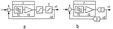
信号のΣΔ変調は、当該信号を少数のビットに符号化するものであるが、そのビット数による理論上の限界より遥かに高い精度を実現することができる。その目的で、フィードバック制御ループが形成される。精度を制限する量子化装置は、図1(a)の一般図に見えるように、ループの出力側に配置される。
【0003】
信号がディジタル信号である場合、ΣΔ変調ユニットはディジタル装置として作成される。ΣΔ変調器へ入力されるディジタル信号がN個のビットからなるものであれば、帰還信号はN−n個の空の最下位ビット(LSB)を含むN個のビットからなり、積分装置1への入力信号はN+1個のビットからなり、量子化装置2の入力と出力の信号はそれぞれN個のビットとn個のビット(ここで、nはNより遥かに小さい)からなるものとなる。従って、ΣΔ変調器の出力で符号化される信号は、ビット数が少ないが、帯域内で高精度を有する。これは、変調器の入力信号が20ビットで符号化されるが、出力が1ビットで得られるCDリーダにおいて一般的である。
【0004】
しかし、信号がアナログ信号であり、アナログ−ディジタル変換機2(精度を制限する量子化)が、図1(b)に見えるように、ループの出力側に配置された場合、入力/出力誤差を積分するフィルタリング11が、必然的にアナログ方式のフィルタリングになる。ここで、2つの可能性がある。第1の可能性は、信号の周波数が低い時であり、この場合、フィルタリング11前にループ(図示せず)の入口で信号をサンプリングし、離散時間系(例えばスイッチトキャパシタを使用して)フィルタリングを行う。第2の可能性は、特にキャリア周波数などの高周波数領域で生じるものであり、この場合、離散時間方式(特に、スイッチトキャパシタまたはスイッチト電流ループ方式)は不適当である。よって、フィルタリング11を連続時間系のフィルタリングとする。このような場合、最も一般的に使用される技術はGmC技術(トランスコンダクタンス増幅器を使用するもの)である。従って、サンプリングは、ループの出力側で、量子化(アナログ−ディジタル変換機)の直前に行われる。
【0005】
また、高周波数についてさらに言及すると、アナログ−ディジタル変換機(ADC)2とディジタル−アナログ変換機(DAC)3の総変換時間は、1サンプリング周期を超え、複数のサンプリング周期に亘って存在する。この問題は、符号化を1ビットに制限することで解決することができるが、その場合、符号化関数が非線形性の強い特性を有するため、ΣΔ変調器の安定性を確実に得ることができる条件を決定することができない。従って、マルチビット符号化が望ましい。この種の符号化において、開ループの応答を、1次線形性の応答とすることができる。
【0006】
そうすると、ループフィルタ11の作成にあたり、ループの安定性を維持しながら利得を最大化する(よって、フィードバック制御信号と制御との間の誤差を最小化する)といったフィードバック制御ループにおける最も一般的な課題を解決しなければならない。これは、潜時値、すなわちループの総遅延時間が、大きいので、実現することが非常に難しい。高潜時値の存在下であっても良好な結果が得られるフィルタリング関数を求めることが困難であるため、現在に至っても連続時間ΣΔ変調器の開発が遅れている。
【0007】
【発明の概要】
本発明は、ループの利得のモジュラスが1となる周波数領域でフィルタの位相を最小化することで、連続時間フィルタリングの困難性を準最適に解決するものである。
【0008】
具体的に、本発明は、入力側に供給された信号を帯域通過積分するための、最小位相変動と称する、位相変動を有する少なくとも1つの素子を具備する連続時間フィルタを提案する。
【0009】
最小位相変動素子とは、周波数がゼロまたは無限大に近づくにつれ、展開位相、すなわち、不明瞭な点を連続性で埋めることで再構成された位相が、ゼロに近づく傾向を有する素子である。
【0010】
帯域通過積分器として実時間のフィルタを作成する場合、−1の臨界点近辺における利得の変動と位相の変動との釣合の問題が生じる。この釣合によってループの安定性が得られなくてはならない。因果関係上、これらの変動はバヤール−ボード(Bayard−Bode)関係によって結ばれている。この問題は、最小位相変更を有する共振装置を少なくとも1つ有する連続時間帯域通過積分フィルタを使用することで解決できる。この最小位相変更を有する共振装置とは、具体的には共振器と抵抗を有するものである。
【0011】
本発明のさらなる目的は、このような連続時間帯域通過積分フィルタを含むフィードバックループを提供することである。このフィードバックループは、特にΣΔ変調器によって構成され得る。フィードバックループを形成する帯域通過ΣΔ変調器は、例えば、アナログ−ディジタル変換機、帰還ディジタル−アナログ変換機および上述したような連続時間帯域通過積分フィルタを具備するものである。
【0012】
【詳細な説明】
帯域通過ΣΔ変調器は、有用帯域内において、従来の符号器に比べて遥かに高い精度で信号のディジタル符号化を可能にする。その実際の機能として、ディジタル化以外にも、量子化雑音を整形することで、有用帯域におけるこの雑音のスペクトル密度を従来の符号器による雑音より遥かに小さくすることである。この有用帯域における量子化雑音のスペクトルパワー密度の低下は、帯域外の雑音のフィルタリングとデシメーションを行った後に、それに相当する精度の向上として現れる。
【0013】
図1は、ある実施例による連続時間帯域通過ΣΔ変調器を示す概略図である。連続時間帯域通過ΣΔ変調器は、フィードバックループからなる。変調器は、ループの順方向チャネルv1に、積分装置1に続いてアナログ/ディジタル変換機(ADC)2を有する。積分装置1は、積分用のフィルタ装置11と、有用帯域における誤差の増幅器12を有する。変調器は、戻りチャネルv2上に、ディジタル/アナログ変換機(ADC)3を有する。この変換機(ADC)3は、ΣΔ変調器の出力で得られた変換信号を変調器の入力まで伝送するために使用される。ループの入力側に、積分装置1の前方に演算器4が配置されており、ΣΔ変調器が例えばレーダまたは通信システム内に使用される場合に、受信機の入力部から送信され、ΣΔ変調器の入力に印加される符号化すべき信号を受信するとともに、さらに、ディジタル/アナログ変換後に戻りチャネルから送信される変換信号も受信する。この演算器4が入力信号と変換信号の差を評価することによって、帯域通過積分装置が、帯域内における出力信号と入力信号との誤差の積分を行う。
【0014】
有用帯域における開ループの利得は1より遥かに大きいので、この有用帯域内では、出力信号と入力信号との誤差が必然的に非常に小さくなる。これがフィードバックループの原理である。従って、ループの出力側の量子化雑音が、この利得に相当する率で排除される。出力信号の量子化雑音は、アナログ/ディジタル変換を行う際に発生する。
【0015】
よって、ループの利得をできるだけ高くすることが必要である。しかし、2つの変換機2および3を行うために必要な時間を考慮すると、好ましいレベルの利得を選択することは不可能である。実際、ループの実用化にあたり、ナイキスト基準を満たさなくてはならない。その結果、所定の変換機2および3について、ループの安定性は専らフィルタリング11と積分処理1の利得12によって決定する。
【0016】
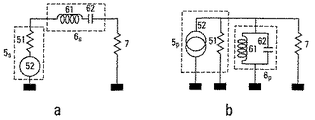
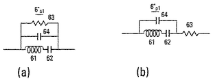
フィルタリングに伴う遅延を最小化し、ループの安定性を保つためには、帯域通過フィルタ11を連続時間装置とする場合、多極フィルタである必要がある。この種の連続時間フィルタは、その原理上、各々が完全な増幅器に挟まれ、1次フィルタを形成する1次共振器のカスケードとして表すことができる。この構造の伝達関数は、各応答の(対数振幅および位相における)総和である。これらの応答は、前記共振器を、直列または並列に、第1に、内部インピーダンス51を有する発電機52と、第2に、負荷7との間に繋ぐことで得ることができる。図2(a)および2(b)に示すLC共振器は、通常の方法によって、この目的で実施される。
【0017】
図2(a)には、直列共振器を示す。インダクタL61とキャパシタC62が直列接続された直列LC回路6Sを有する。図2(b)には、並列共振器を示す。インダクタL61とキャパシタC62が並列接続された並列LC回路6Pを有する。
【0018】
しかし、このような簡単なLC共振器6を有する連続時間フィルタ11は、位相の変動が最小化されたものではない。実用上、共振周波数または反共振周波数から離れた状態で位相がゼロに戻ることが好ましい。実際、これが確認されなければ、フィルタが設置されたループは安定性を示す。
【0019】
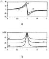
図3(a)には、図2に示す共振装置の位相応答を、周波数の関数として示す。周波数軸は、共振周波数に対して正規化されている。図3(a)に示す位相は、周波数が0に近づくにつれ、90°に寄り、周波数が無限大に向かうにつれ、−90°に寄る。位相変動を最小化するためには、周波数がゼロまたは無限大に向かうにつれ、位相がゼロに寄る必要がある。よって、図3(a)において、図2に示すような簡単なLC共振器を有するフィルタは、いわゆる「最小」位相変動を有するものではない。
【0020】
図3(b)には、図2の共振装置の振幅応答を、周波数の関数として示す。周波数軸は、共振周波数に対して正規化されている。振幅は、共振周波数から離れても飽和しない。振幅応答の波形は、因果関係により、図2(a)に見えるような位相変動を説明することができる。
【0021】
高安定性と同時に充分の利得を実現するためには、フィルタ11は最小位相変動を有する連続時間帯域通過積分フィルタでなければいけない。具体的に、次のような伝達関数を有する。

ここで得られる関数は、QNとQDの値によって変化する。実際、QD≧QNの場合、共振周波数周辺で、周波数とともに位相が低下するので、位相遅れを有する帯域フィルタリング関数が得られる。QD≦QNの場合に得られるフィルタは、位相進みを有する帯域阻止性のものになる。QDは、共振器6(または共振装置)の振幅における伝達関数の極大を示す。この比率QD/QNは、共振器6(または共振装置)の振幅における伝達関数の極大と極小との間の比率を示す。
【0023】
本発明は、これを、共振器6に代わって共振装置6’s1、6’s2、6’p1、6’p2、6”sおよび6”pを使用することで実現することを提案する。
【0024】
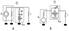
本発明の第1、第2、第3および第4の変形を、図4(a)、4(b)、6(a)および6(b)に示す。これらの装置は、共振装置6’s1、6’s2、6’p1または6’p2を構成するために、LC回路6に、直列または並列に抵抗を追加したものである。
【0025】
本発明によるフィルタの第1変形は、図4(a)に示すように、直列共振器61〜62に抵抗63を並列配置したものである。その結果、共振状態の場合、共振装置6’s1の作用において共振器61〜62が優勢になる。また、回路が共振状態から遠く、共振器61〜62のインピーダンスが大きい場合、抵抗63の作用が優勢になる。これは、図5(a)および5(b)に示してある。
【0026】
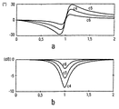
図5(a)には、フィルタ11の当該変形の、QN=7の場合の位相の応答を、周波数の関数として示す。曲線c1、c2およびc3で示す応答は、QDの値が、それぞれ10、20および14である場合のフィルタ11の応答に相当する。周波数軸は、共振周波数に対して正規化されている。共振装置6’s1は、図5(a)に示すように、最小位相変動素子である。実際、周波数が0または無限大に向かうにつれ、位相は0に近づく。
【0027】
図5(b)には、フィルタ11の当該変形の、QN=7の場合の振幅の応答を、周波数の関数として示す。曲線c1、c2およびc3で示す応答は、QDの値が、それぞれ10、20および14である場合のフィルタ11の応答に相当する。周波数軸は、共振周波数に対して正規化されている。
【0028】
同様に、並列共振器61〜62に抵抗63を直列接続することによって、図4(b)に示す共振装置6’p1を構成することが可能である。
【0029】
この種の共振装置6’1の伝達関数は、一般的に次のような形式を有する。
これらの共振装置6’の部品を、図6(a)および6(b)に示すように変更、配置すると、フィルタに位相進みを伴う帯域阻止作用を持たせることができる。図6(a)の発明によるフィルタ11の第3変形において、抵抗63は並列配置されるLC直列共振器61〜62と直列接続される。その結果、共振状態では、共振装置6’s2の作用において抵抗63が優勢になる。また、動作条件が共振状態から遠い場合、共振器61〜62の働きが抵抗63より大きくなる。これは、フィルタ11のこの変形における、図7(a)に示すような位相および、図7(b)に示すような振幅の周波数応答によって表すことができる。
【0031】
図7(a)には、当該変形による共振装置6’s2を有するフィルタ11における、QN=7の場合の位相応答を、周波数の関数として示す。曲線c4、c5およびc6に示す応答は、それぞれ、QD=2.5、3.5および5であるフィルタ11に対応するものである。周波数軸は、共振周波数に対して正規化されている。共振装置6’s2は、図7(a)に示すとおり、最小位相変動素子である。実際、周波数が0または無限大に向かうにつれ、位相は0に近づく。
【0032】
図7(b)には、当該変形による共振装置6’s2を有するフィルタ11における、QN=7の場合の振幅応答を、周波数の関数として示す。曲線c4、c5およびc6に示す応答は、それぞれ、QD=2.5、3.5および5であるフィルタ11に対応するものである。周波数軸は、共振周波数に対して基準化されている。
【0033】
従って、どの種類の共振装置(例えば、位相遅れ装置、位相進み装置等)を望むかによって、共振装置の構造を、1つまたは複数の所定の周波数帯域(それぞれ、共振周波数を含まない周波数帯域、共振周波数を含む周波数帯域等)において抵抗63の作用が共振器より優勢になるようにする。
【0034】
同様にして、図6(b)に示すように、共振装置6’p2に対して直列配置された並列型のLC共振器61〜62に対して、抵抗63を並列配置することができる。
【0035】
この種の共振装置6’2は、次の形式の伝達関数を有する。
複数の基本素子、すなわち共振装置を組み合わせることで高次フィルタ11が得られる。従って、本発明による高次フィルタ11の製造は、上記共振装置の第1ないし第4変形6’s1、6’s2、6’p1、6’p2を1つ以上カスケードさせる過程を含む。この高次フィルタを得るために使用されるカスケードは、伝達関数の乗算を可能にする増幅器、または図8に示すような梯子構造に直接組立てたり、図12に示すようなバランスブリッジ構造として組立てることによって実現することができる。
【0037】
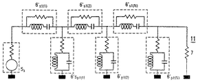
図8において、フィルタ素子を構成するのは共振装置6’s1、6’p1のみであるが、次の組合せを、一般的な応用において、位相進み素子6’s2、6’p2にも難なく適用することが可能であることは明かである。また、両種類に適用することも可能である。図8に示すフィルタ11は、交互に配置された共振装置6’s1、6’p1からなる梯子構造のカスケードである。各対の共振装置6’s1、6’p1が段を形成する。フィルタ11は、N段によって構成される。
【0038】
実用上、品質因子の値が高いインダクタを含ませることは難しい。そのため、過電圧の高い共振器の(インダクタおよびキャパシタによる)製造は不可能である。共振器の過電圧は、特に変換時間が長い場合、過電圧が大きいほど臨界領域における位相が小さくなるので、ΣΔ変調器のループ安定性を得るための基本条件である。それが、非常に高い過電圧を有するモノリシックまたは一体型の共振器技術を使用する理由である。これらの技術に属する装置として、バルク波共振器(BAW)やそのTFR(薄膜共振器)またはFBAR(基本バルク波共振器)またはHBAR(高次バルク波共振器)形態、表面波共振器(SAW)、誘電体共振器、MEMS(マイクロエレクトロメカニカルシステム)共振器等があるが、これらに限定されるものではない。しかし、多くの場合、このような共振器は、単純な直列または並列LC回路61〜62ではなく、図9に示すように、LC素子61〜62を有する直列構造の共振枝と並列の静電キャパシタ64からなる等価図を有するものである。従って、共振と反共振を両方有するものである。
【0039】
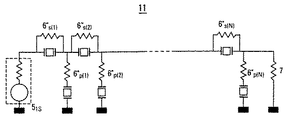
よって、共振装置6”sおよび6”pは、フィルタリングの場合は直列型、位相進みの場合は並列型の特性を有する直列LC共振器61〜62を得るために図10(a)に示すように変更され、フィルタリングの場合は並列型、位相進みの場合は直列型の特性を有する並列LC共振器61〜62を得るために図10(b)に示すように変更される。これらの共振装置6”s、6”pは、1次フィルタまたは上述したような高次フィルタであるフィルタ11において使用され、増幅器を介してカスケードされるか、図11に示すように梯子状に直接接続される。この図11において、装置全体の性能を最適化するためにすべての共振装置6”s、6”pを異なるものにすることができる。さらに、この図において、位相遅れフィルタと位相進みフィルタとの間に構造上の差異はもはや存在せず、その差は共振器の抵抗値とインピーダンス値との比、該当する周波数帯域およびフィルタにおける抵抗−共振器対の配置によって決まるものである。
【0040】
従って、図11を、共振装置6”s、6”pの静電キャパシタンス64またはその直列キャパシタンス62の値がゼロである一般図として捉えることもできる。これが、すべての共振装置6”s、6”pに対して行われる場合、図8を参照して説明するように、使用される構造はインダクタおよびキャパシタ構造としてもっとも一般的なものである。
【0041】
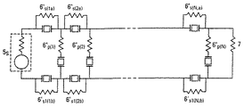
勿論、図11の一般構造は、差動モードの操作のために、自明の方法で対称化し、図11の共振装置6”pの倍のインピーダンスを有する共振装置6”pを有する図12の構造にすることも可能である。さらに、図12において、電源装置5sのインピーダンス51とフィルタのインピーダンス7も、それぞれ、図11におけるインピーダンスの倍である。
【0042】
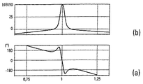
この種のフィルタ構造によって得られる通常の周波数応答を、位相におけるものを図13(a)に、振幅におけるものを図13(b)に示す。これは、fsを標本化周波数とした時に、中央周波数f0=3fs/8を有するΣΔ変調器の開ループ応答を近似する線形応答である。このようなΣΔ変調器の構造例を図14に示す。この図面において、このΣΔ変調器、アナログ−ディジタル変換機2およびディジタル−アナログ変換機3によって形成される対は、累積的な総合処理時間が4.82個の標本化周期である。この応答は、アナログ−ディジタル変換機2によるスペクトルのエイリアシングやディジタル−アナログ変換機3によるシンク(Sinc)フィルタリングを考慮したものである。
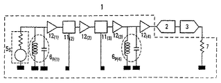
【0043】
図14に提案される実施例において、ループフィルタ11は2つのフィルタ11(2)および11(3)からなる。各フィルタ11は、3つの部分に分けることができる。ループフィルタ11は、さらに、第1の増幅器12(1)、第1のフィルタ11(2)、第2の増幅器12(2)、第2のフィルタ11(3)および第3の増幅器12(3)を、順番に配置した直列回路を挟んだ両側に2つの共振セル6p(1)および6p(4)を具備する。
【0044】
各フィルタ11(2)および11(3)の3つの部分は、いずれも、図11に示すような直列装置6”sおよび並列装置6”pからなる2つの共振装置を有する。共振セル6p(1)および6p(4)は、アナログ−ディジタル変換機2によって設けられるスペクトルのエイリアシングによる応答への影響を最小化するように設計されるため、低過電圧セルである。従って、閉ループの場合の変調器の動作は、位相において±20度、振幅において±3dBの限界を以って安定である。
【0045】
次の表は、フィルタ11(2)および11(3)の各部分の要素の代表的な値を示すものである。
差動モードによる操作の特例の場合に、他の構造を提案することができる。その構造とは、バランスブリッジ構造であり、その原理を図15に示す。バランスブリッジは、共振装置6”s(a)および6”s(b)の静電キャパシタ64と、同値のさらなるキャパシタ621および623を有する。共振装置6”s(a)および6”s(b)における2つの抵抗63(a)および63(b)と2つの共振アーム61〜62(a)および61〜62(b)の存在によって、ブリッジがアンバランスになる。その結果、帯域内で応答を得ることができ、さらに、近範囲の拒絶による準プラトーで応答を制限することで、位相変動を抑えることができる。
【0047】
通過帯域、すなわち共振装置6”s(a)および6”s(b)の共振周辺において、追加された静電キャパシタ621および623のインピーダンスを、2つのインダクタ611および613によって補償することができる。この操作態様が、LCωr 2=1における最適の操作である。
【0048】
これらのブリッジ構造は、通常は異なる中央周波数でカスケード接続することによって、高次フィルタリングを実現することができる。
【0049】
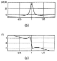
図16(a)および16(b)は、中央周波数f0=3fs/4の、累積的総合処理時間が7.5標本化周期であるアナログ−ディジタル変換機2とディジタル−アナログ変換機3からなる対を有するΣΔ変調器の、開ループにおける、位相および振幅の周波数応答の例をそれぞれ示すものである。ΣΔ変調器は、さらに、図15に示すブリッジ型構造を4つ有するカスケードによって得られるフィルタ11を含むものである。共振器の周波数およびインピーダンス値は、次の条件を満たすものである:ωa 2/ωr 2−1=1/150、RCωr=0.943および(ωr−ω0)/ω0=±2.53×10−3および±2.94×10−3。
【0050】
図16(a)および16(b)に示す応答を読取ると、閉ループ変調器の操作が安定しており、次の限界を有することが示されている:位相において±20度、振幅において±3dB。
【0051】
ΣΔ変調器の変換機は、標本化周期より長い遅延を設けるように選択することができる。ΣΔ変調器のある実施形態によると、ΣΔ変調器の1つの要素または特定の要素またはすべての要素が、半導体内に集積される。
【0052】
抵抗63は、圧電基板上またはセラミックパック内またはその上に取り付けることができる。キャパシタ62は、セラミックパック内またはその上に取り付けることができる。1つまたは複数の共振器61〜62は、セラミック共振器または表面波共振器(SAW)またはバルク波共振器(BAW)、またはその変形であるFBAR(基本バルク波共振器)またはHBAR(高次バルク波共振器)またはTFR(薄膜共振器)、または誘電体共振器、または超伝導体材料からなる共振器、またはGmC型共振器(キャパシタ+トランスコンダクタンス増幅器)であってもよい。さらに、音響共振器(SAW、BAW、TFR、FBAR、HBAR)の圧電基板は、シリコン上に集積されたものであってもよい。
【0053】
フィルタ要素(抵抗、キャパシタおよびインダクタ)を圧電基板上に製造することによって、要素間の相互接続の手間がなくなり、フィルタの製造を容易化する。フィルタの要素(抵抗、キャパシタおよびインダクタ)を圧電基板上またはセラミックパック内に形成する利点の1つは、フィルタの伝達関数を制御し易くなることである。さらに、圧電基板上に形成されたフィルタは、ΣΔ変調器の1つまたは複数の要素を含んだ半導体上に搭載されたものだってもよい。
【0054】
ここであげる応用例は、ΣΔ変調器によって示したが、あらゆる種類のフィードバックループに適用することも可能である。本発明により、ループが不安定になることなく、フィードバックループの潜時値を1より大きくすることができる。
【図面の簡単な説明】
【図1】図1(a)および1(b)は、それぞれ、あらゆる種類の信号と、アナログ信号を処理するための連続時間帯域通過ΣΔ変調器を示す一般図である。
【図2】図2(a)および2(b)は、従来技術による1次連続時間帯域通過積分フィルタを示すものである。
【図3】図3(a)および3(b)は、それぞれ、図2のフィルタの位相と振幅における周波数応答を示すものである。
【図4】図4(a)および4(b)は、本発明による1次連続時間帯域通過積分フィルタの第1変形と第2変形を示すものである。
【図5】図5(a)および5(b)は、それぞれ、図4のフィルタの位相と振幅における周波数応答を、共振器Qdの過電圧の関数として示すものである。
【図6】図6(a)および6(b)は、本発明による1次連続時間帯域通過積分フィルタの第3変形と第4変形を示すものである。
【図7】図7(a)および7(b)は、それぞれ、図6のフィルタの位相と振幅における周波数応答を、共振器Qdの過電圧の関数として示すものである。
【図8】図8は、本発明による高次連続時間帯域通過積分フィルタの第5変形を示すものである。
【図9】図9は、従来技術による共振器の等価回路を示すものである。
【図10】図10(a)および10(b)は、本発明による等価共振装置の2つの実施形態を示すものである。
【図11】図11は、図10の等価共振装置を使用した梯子構造を有する差動モードの高次連続時間帯域通過積分フィルタの第6の変形を示すものである。
【図12】図12は、図10の等価共振装置を使用した梯子構造を有する差動モードの高次連続時間帯域通過積分フィルタの第7の変形を示すものである。
【図13】図13(a)および13(b)は、それぞれ、図12のフィルタの位相と振幅における周波数応答を示すものである。
【図14】図14は、図11の高次連続時間帯域通過積分フィルタを使用した連続時間帯域通過積分ΣΔ変調器を示すものである。
【図15】図15は、図10の等価共振装置を使用したブリッジ構造を有する差動モードの高次連続時間帯域通過積分フィルタの第8の変形を示すものである。
【図16】図16(a)および16(b)は、それぞれ、図15のフィルタの位相と振幅における周波数応答を示すものである。[0001]
TECHNICAL FIELD OF THE INVENTION
The present invention relates to continuous-time filtering. More specifically, the present invention relates to filtering in a feedback control loop such as a sigma-delta (ΣΔ) modulator. An analog ΣΔ modulator can be used, for example, in a radar receiver or a communication system to improve the accuracy of analog-digital coding, in particular.
[0002]
[Description of the Prior Art]
ΣΔ modulation of a signal encodes the signal into a small number of bits, but can achieve much higher accuracy than the theoretical limit based on the number of bits. To that end, a feedback control loop is formed. The quantizer which limits the accuracy is located on the output side of the loop, as can be seen in the general diagram of FIG.
[0003]
If the signal is a digital signal, the ΣΔ modulation unit is made as a digital device. If the digital signal input to the ΣΔ modulator is composed of N bits, the feedback signal is composed of N bits including Nn empty least significant bits (LSBs). Is composed of N + 1 bits, and the input and output signals of the
[0004]
However, if the signal is an analog signal and the analog-to-digital converter 2 (quantization limiting accuracy) is placed on the output side of the loop, as seen in FIG. The
[0005]
Further, referring further to the high frequency, the total conversion time of the analog-digital converter (ADC) 2 and the digital-analog converter (DAC) 3 exceeds one sampling period and exists over a plurality of sampling periods. This problem can be solved by restricting the encoding to one bit, but in this case, the stability of the ΣΔ modulator can be reliably obtained because the encoding function has a strong characteristic of non-linearity. The condition cannot be determined. Therefore, multi-bit encoding is desirable. In this type of coding, the open loop response can be a first order linear response.
[0006]
Then, when creating the
[0007]
Summary of the Invention
The present invention solves the difficulty of continuous-time filtering in a sub-optimal manner by minimizing the phase of a filter in the frequency domain where the modulus of the loop gain is 1.
[0008]
In particular, the present invention proposes a continuous-time filter comprising at least one element having a phase variation, referred to as minimum phase variation, for band-pass integration of the signal supplied to the input.
[0009]
The minimum phase variation element is an element in which, as the frequency approaches zero or infinity, the developed phase, that is, the phase reconstructed by filling the obscured points with continuity, tends to approach zero.
[0010]
When a real-time filter is created as a band-pass integrator, there is a problem of a balance between a gain variation and a phase variation near a critical point of -1. This balance must provide loop stability. Due to the causal relationship, these fluctuations are connected by a Bayard-Board relationship. This problem can be solved by using a continuous time bandpass integrating filter having at least one resonator with a minimum phase change. The resonance device having the minimum phase change specifically has a resonator and a resistor.
[0011]
It is a further object of the present invention to provide a feedback loop that includes such a continuous time bandpass integration filter. This feedback loop can in particular be constituted by a ΣΔ modulator. The band-pass ΣΔ modulator forming the feedback loop includes, for example, an analog-to-digital converter, a feedback digital-to-analog converter, and a continuous-time band-pass integration filter as described above.
[0012]
[Detailed description]
Bandpass ΣΔ modulators allow digital encoding of signals within the useful band with much higher accuracy than conventional encoders. Its actual function, besides digitization, is to shape the quantization noise so that the spectral density of this noise in the useful band is much smaller than the noise from conventional encoders. This reduction in the spectral power density of the quantization noise in the useful band appears as a corresponding increase in accuracy after filtering and decimation of out-of-band noise.
[0013]
FIG. 1 is a schematic diagram illustrating a continuous time bandpass ΣΔ modulator according to one embodiment. A continuous time bandpass ΣΔ modulator consists of a feedback loop. The modulator has an
[0014]
Since the gain of the open loop in the useful band is much greater than one, the error between the output signal and the input signal is necessarily very small in this useful band. This is the principle of the feedback loop. Therefore, quantization noise at the output of the loop is eliminated at a rate corresponding to this gain. The quantization noise of the output signal is generated when performing the analog / digital conversion.
[0015]
Therefore, it is necessary to make the gain of the loop as high as possible. However, considering the time required to perform the two
[0016]
In order to minimize the delay caused by the filtering and maintain the loop stability, when the
[0017]
FIG. 2A shows a series resonator.
[0018]
However, the continuous-
[0019]
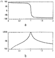
FIG. 3 (a) shows the phase response of the resonator shown in FIG. 2 as a function of frequency. The frequency axis is normalized with respect to the resonance frequency. The phase shown in FIG. 3A shifts toward 90 ° as the frequency approaches 0, and shifts toward −90 ° as the frequency approaches infinity. To minimize phase fluctuations, the phase must approach zero as the frequency approaches zero or infinity. Thus, in FIG. 3 (a), a filter having a simple LC resonator as shown in FIG. 2 does not have a so-called "minimum" phase variation.
[0020]
FIG. 3 (b) shows the amplitude response of the resonator of FIG. 2 as a function of frequency. The frequency axis is normalized with respect to the resonance frequency. The amplitude does not saturate away from the resonance frequency. The waveform of the amplitude response can explain the phase fluctuation as shown in FIG.
[0021]
In order to realize high gain at the same time as high stability, the
The function obtained here is QNAnd QDVaries depending on the value of. In fact, QD≧ QNIn the case of, the phase decreases with the frequency around the resonance frequency, so that a band-pass filtering function having a phase lag is obtained. QD≤QNThe resulting filter will be band rejection with phase lead. QDIndicates the maximum of the transfer function at the amplitude of the resonator 6 (or the resonance device). This ratio QD/ QNDenotes the ratio between the maximum and the minimum of the transfer function at the amplitude of the resonator 6 (or the resonance device).
[0023]
In the present invention, the
[0024]
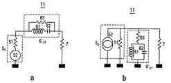
First, second, third and fourth variants of the invention are shown in FIGS. 4 (a), 4 (b), 6 (a) and 6 (b). These devices comprise a resonance device 6 's1, 6 's2, 6 'p1Or 6 'p2In this embodiment, a resistor is added to the
[0025]
A first modification of the filter according to the present invention is one in which a
[0026]
FIG. 5A shows Q of the deformation of the filter 11.NThe phase response for = 7 is shown as a function of frequency. The response shown by curves c1, c2 and c3 is QDAre 10, 20, and 14, respectively, corresponding to the response of the
[0027]
FIG. 5B shows the Q of the deformation of the filter 11.NThe amplitude response for = 7 is shown as a function of frequency. The response shown by curves c1, c2 and c3 is QDAre 10, 20, and 14, respectively, corresponding to the response of the
[0028]
Similarly, by connecting the
[0029]
This type of resonance device 6 '1Generally has the following form:
By changing and arranging the components of the resonance device 6 'as shown in FIGS. 6A and 6B, the filter can be provided with a band rejection function with a phase lead. In a third modification of the
[0031]
FIG. 7A shows a
[0032]
FIG. 7B shows a
[0033]
Thus, depending on what type of resonant device (e.g., phase lag device, phase lead device, etc.) is desired, the structure of the resonant device may be adjusted to one or more predetermined frequency bands (each a frequency band that does not include the resonant frequency, In the frequency band including the resonance frequency, the action of the
[0034]
Similarly, as shown in FIG. 6B, the resonance device 6 'p2The
[0035]
This type of resonance device 6 '2Has a transfer function of the form
The high-
[0037]
In FIG. 8, the filter device is composed of a
[0038]
In practice, it is difficult to include inductors with high quality factor values. Therefore, it is not possible to manufacture a resonator having a high overvoltage (by using an inductor and a capacitor). The overvoltage of the resonator is a basic condition for obtaining the loop stability of the ΣΔ modulator because the phase in the critical region becomes smaller as the overvoltage increases, especially when the conversion time is long. That is the reason for using monolithic or integrated resonator technology with very high overvoltages. Devices belonging to these technologies include a bulk wave resonator (BAW) and its TFR (thin film resonator) or FBAR (basic bulk wave resonator) or HBAR (higher order bulk wave resonator) form, a surface wave resonator (SAW). ), A dielectric resonator, a MEMS (microelectromechanical system) resonator, and the like, but are not limited thereto. However, in many cases, such a resonator is not a simple series or parallel LC circuit 61-62, but rather, as shown in FIG. 9, an electrostatic capacitor in parallel with a series-structured resonance branch having LC elements 61-62. It has an equivalent diagram composed of a
[0039]
Therefore, the
[0040]
Therefore, FIG.s, 6 "pCan be considered as a general diagram in which the value of the
[0041]
Of course, the general structure of FIG. 11 is symmetrical in a trivial manner for differential mode operation, and the
[0042]
FIG. 13A shows a normal frequency response obtained by this type of filter structure in a phase, and FIG. This is fsIs the sampling frequency, the center frequency f0= 3fs9 is a linear response approximating the open loop response of a ΣΔ modulator having / 8. FIG. 14 shows an example of the structure of such a ΣΔ modulator. In this drawing, the pair formed by the ΣΔ modulator, the analog-
[0043]
In the embodiment proposed in FIG. 14, the
[0044]
Each of the three parts of each filter 11 (2) and 11 (3) is a
[0045]
The following table shows typical values of the elements of each part of the filters 11 (2) and 11 (3).
In the case of special cases of operation in differential mode, other structures can be proposed. The structure is a balance bridge structure, and its principle is shown in FIG. The balance bridge is a
[0047]
Passband, ie,
[0048]
These bridge structures can achieve higher order filtering, usually by cascading at different center frequencies.
[0049]
FIGS. 16 (a) and 16 (b) show the center frequency f0= 3fsPhase and amplitude frequency in open loop of a ΣΔ modulator having a pair consisting of an analog-to-
[0050]
Reading the responses shown in FIGS. 16 (a) and 16 (b) shows that the operation of the closed loop modulator is stable and has the following limits: ± 20 degrees in phase and ± 3 dB in amplitude. .
[0051]
The converter of the ΣΔ modulator can be selected to provide a delay longer than the sampling period. According to one embodiment of the ΣΔ modulator, one element or specific elements or all elements of the ΣΔ modulator are integrated in a semiconductor.
[0052]
The
[0053]
Fabricating the filter elements (resistors, capacitors and inductors) on a piezoelectric substrate eliminates the need for interconnection between the elements and simplifies the manufacture of the filter. One of the advantages of forming the filter elements (resistors, capacitors and inductors) on a piezoelectric substrate or in a ceramic pack is that the transfer function of the filter is easier to control. Further, the filter formed on the piezoelectric substrate may be mounted on a semiconductor including one or more elements of the ΣΔ modulator.
[0054]
Although the application example given here has been described with a ΣΔ modulator, it can be applied to any kind of feedback loop. According to the present invention, the latency value of the feedback loop can be made larger than 1 without the loop becoming unstable.
[Brief description of the drawings]
FIGS. 1 (a) and 1 (b) are general diagrams showing a continuous time bandpass ΣΔ modulator for processing all types of signals and analog signals, respectively.
FIGS. 2 (a) and 2 (b) show a first order continuous time bandpass integration filter according to the prior art.
3 (a) and 3 (b) show the frequency response in phase and amplitude of the filter of FIG. 2, respectively.
FIGS. 4 (a) and 4 (b) show first and second variations of a first order continuous time bandpass integration filter according to the present invention.
5 (a) and 5 (b) show the frequency response in phase and amplitude of the filter of FIG.dAs a function of the overvoltage.
FIGS. 6 (a) and 6 (b) show a third and a fourth modification of a first-order continuous-time bandpass integration filter according to the present invention.
7 (a) and 7 (b) show the frequency response in phase and amplitude of the filter of FIG.dAs a function of the overvoltage.
FIG. 8 shows a fifth modification of the high-order continuous-time bandpass integration filter according to the present invention.
FIG. 9 shows an equivalent circuit of a resonator according to the related art.
10 (a) and 10 (b) show two embodiments of an equivalent resonance device according to the present invention.
11 shows a sixth modification of the differential mode high-order continuous-time bandpass integration filter having the ladder structure using the equivalent resonance device of FIG. 10;
FIG. 12 shows a seventh modification of the differential mode high-order continuous-time bandpass integration filter having the ladder structure using the equivalent resonance device of FIG. 10;
FIGS. 13 (a) and 13 (b) show the frequency response in phase and amplitude of the filter of FIG. 12, respectively.
FIG. 14 shows a continuous time bandpass integral ΣΔ modulator using the higher order continuous time bandpass integral filter of FIG. 11;
FIG. 15 shows an eighth modification of the differential mode high-order continuous time bandpass integration filter having the bridge structure using the equivalent resonance device of FIG. 10;
16 (a) and 16 (b) show the frequency response of the filter of FIG. 15 in phase and amplitude, respectively.
Claims (16)
−抵抗に対して並列接続された直列共振器であって、直列接続されたインダクタおよびキャパシタを有する直列共振器、または
−抵抗に対して直列接続された並列共振器であって、並列接続されたインダクタおよびキャパシタを有する並列共振器を有する、上記請求項に記載のフィルタ。The resonance device having the minimum phase variation and having a phase delay,
A series resonator connected in parallel with the resistor, wherein the series resonator has an inductor and a capacitor connected in series, or a parallel resonator connected in series with the resistor, which is connected in parallel. A filter according to any preceding claim, comprising a parallel resonator having an inductor and a capacitor.
−抵抗に対して直列接続された直列共振器であって、直列接続されたインダクタおよびキャパシタを有する直列共振器、または
−抵抗に対して並列接続された並列共振器であって、並列接続されたインダクタおよびキャパシタを有する並列共振器を有する、上記請求項に記載のフィルタ。The resonance device having the minimum phase variation and having a phase lead,
A series resonator connected in series with the resistor, the series resonator having an inductor and a capacitor connected in series, or a parallel resonator connected in parallel with the resistor, connected in parallel. A filter according to any preceding claim, comprising a parallel resonator having an inductor and a capacitor.
−直列接続されたインダクタとキャパシタを有する直列共振器を含む第1アーム、
−第1アームの直列共振器に対して並列接続された第2アームであって、キャパシタを含む第2アーム、および
−第1アームの直列共振器および第2アームのキャパシタに対して並列接続されているか、直列共振器およびキャパシタによって形成される装置に対して直列接続されている抵抗を含む等価図を有する請求項2または3に記載のフィルタ。The resonance device having the minimum phase variation,
A first arm including a series resonator having an inductor and a capacitor connected in series;
A second arm connected in parallel with the series resonator of the first arm, the second arm including a capacitor; and a second arm connected in parallel with the series resonator of the first arm and the capacitor of the second arm. 4. A filter as claimed in claim 2 or 3 having an equivalent diagram including a resistor connected or connected in series to a device formed by a series resonator and a capacitor.
−セラミック共振器、
−表面波共振器(SAW)、
−バルク波共振器(BAW)、
−基本バルク共振器(FBAR)、
−高次バルク共振器(HBAR)、
−薄膜共振器(TFR)、
−誘電体共振器、
−超伝導体材料からなる共振器、および
−GmC型共振器からなる群より選択された共振器である上記請求項のうちいずれか1項に記載のフィルタ。One or more resonators
A ceramic resonator,
A surface acoustic wave resonator (SAW),
A bulk wave resonator (BAW),
A basic bulk resonator (FBAR),
A high-order bulk resonator (HBAR),
A thin film resonator (TFR),
A dielectric resonator,
The filter according to any one of the preceding claims, wherein the filter is a resonator selected from the group consisting of a superconductor material and a GmC resonator.
フィルタが、半導体上に搭載された圧電基板上またはΣΔ変調器のセラミックパッケージ内に形成される上記請求項に記載の帯域通過ΣΔ変調器。One or more of the elements forming the ΣΔ modulator, or all the elements forming the ΣΔ modulator, are integrated in a semiconductor;
The band-pass ΣΔ modulator according to claim 1, wherein the filter is formed on a piezoelectric substrate mounted on a semiconductor or in a ceramic package of the ΣΔ modulator.
Applications Claiming Priority (1)
| Application Number | Priority Date | Filing Date | Title |
|---|---|---|---|
| FR0202957A FR2837035B1 (en) | 2002-03-08 | 2002-03-08 | INTEGRATOR FILTER WITH CONTINUOUS TIME AND MINIMUM PHASE VARIATION, SIGMA-DELTA PASSER MODULE USING SUCH A FILTER |
Publications (1)
| Publication Number | Publication Date |
|---|---|
| JP2004040764A true JP2004040764A (en) | 2004-02-05 |
Family
ID=27741462
Family Applications (1)
| Application Number | Title | Priority Date | Filing Date |
|---|---|---|---|
| JP2003064201A Pending JP2004040764A (en) | 2002-03-08 | 2003-03-10 | Minimum phase fluctuation continuous time integration filter and bandpass ΣΔ modulator using the filter |
Country Status (9)
| Country | Link |
|---|---|
| US (1) | US7136001B2 (en) |
| EP (1) | EP1343250B1 (en) |
| JP (1) | JP2004040764A (en) |
| KR (1) | KR20030074310A (en) |
| AT (1) | ATE431010T1 (en) |
| CA (1) | CA2420364A1 (en) |
| DE (1) | DE60327485D1 (en) |
| FR (1) | FR2837035B1 (en) |
| SG (1) | SG114603A1 (en) |
Cited By (5)
| Publication number | Priority date | Publication date | Assignee | Title |
|---|---|---|---|---|
| JP2006319498A (en) * | 2005-05-11 | 2006-11-24 | Audio Technica Corp | Infrared signal selector |
| JP2010528577A (en) * | 2007-05-23 | 2010-08-19 | アドバンスト・エナジー・インダストリーズ・インコーポレイテッド | Common mode filter system and method for solar energy inverter |
| US8072363B2 (en) | 2007-08-10 | 2011-12-06 | National University Of Singapore | System and method for bandpass sigma-delta modulation |
| JP2012175119A (en) * | 2011-02-17 | 2012-09-10 | Murata Mfg Co Ltd | Filter property compensation circuit and filter circuit |
| JP2013246166A (en) * | 2012-05-25 | 2013-12-09 | Freescale Semiconductor Inc | Vehicle-borne radar systems with continuous-time, sigma delta analog-to-digital converters, and methods of their operation |
Families Citing this family (21)
| Publication number | Priority date | Publication date | Assignee | Title |
|---|---|---|---|---|
| FR2880219B1 (en) * | 2004-12-23 | 2007-02-23 | Thales Sa | METHOD AND SYSTEM FOR DIGITAL RADIOCOMMUNICATION, IN PARTICULAR FOR MOBILE SOIL STATIONS |
| DE102005003630A1 (en) * | 2005-01-26 | 2006-07-27 | Robert Bosch Gmbh | Electromechanical delta-sigma-modulator for e.g. airbag control system of motor vehicle, has multibit-DAC to adjust amplification in servo loop and bandwidth of modulator independent of input signal of multibit-ADC |
| JP4079953B2 (en) * | 2005-02-17 | 2008-04-23 | 株式会社半導体理工学研究センター | High frequency circuit |
| US20060288090A1 (en) * | 2005-06-20 | 2006-12-21 | Kraft Harold H | Privacy Information Reporting Systems with Refined Content Model |
| US7633773B2 (en) * | 2006-05-10 | 2009-12-15 | Micron Technology, Inc. | On-die anti-resonance structure for integrated circuit |
| US8203069B2 (en) * | 2007-08-03 | 2012-06-19 | Advanced Energy Industries, Inc | System, method, and apparatus for coupling photovoltaic arrays |
| US8461508B2 (en) | 2008-08-10 | 2013-06-11 | Advanced Energy Industries, Inc. | Device, system, and method for sectioning and coupling multiple photovoltaic strings |
| US7619200B1 (en) * | 2008-08-10 | 2009-11-17 | Advanced Energy Industries, Inc. | Device system and method for coupling multiple photovoltaic arrays |
| FR2938083B1 (en) * | 2008-10-31 | 2013-03-29 | Thales Sa | METHOD FOR IMPROVING RESOLUTION AND CORRECTING DISTORTIONS FOR SIGMA-DELTA MODULATOR AND SIGMA-DELTA MODULATOR USING THE METHOD |
| US8580596B2 (en) * | 2009-04-10 | 2013-11-12 | Nxp, B.V. | Front end micro cavity |
| CN101771394A (en) | 2010-02-05 | 2010-07-07 | 无锡市好达电子有限公司 | Superlattice crystal resonator and application as superlattice crystal filter |
| US8599055B1 (en) * | 2012-07-24 | 2013-12-03 | Kathrein-Werke Kg | Digital-to-analog converter |
| FR2996387B1 (en) | 2012-09-28 | 2015-08-07 | Univ Pierre Et Marie Curie Paris 6 | CAPACITIVE COUPLING SIGMA DELTA RF MODULATOR, ANALOGUE-DIGITAL CONVERTER AND APPARATUS COMPRISING SUCH A MODULATOR |
| US9276547B2 (en) * | 2013-06-28 | 2016-03-01 | Peregrine Semiconductor Corporation | Systems and methods of stacking LC tanks for wide tuning range and high voltage swing |
| US9391656B2 (en) * | 2014-08-11 | 2016-07-12 | Syntropy Systems, Llc | Distributed noise shaping apparatus |
| FR3030941B1 (en) * | 2014-12-22 | 2018-10-05 | Thales | SIGMA-DELTA LOADING LOOP AND MODULATOR COMPRISING SUCH A LOADING LOOP. |
| US10389555B2 (en) | 2016-01-28 | 2019-08-20 | Hewlett Packard Enterprise Development Lp | Phase delay difference-based channel compensation |
| US11133777B2 (en) | 2017-04-21 | 2021-09-28 | Fan Wang | Solar array communications |
| US20180309301A1 (en) * | 2017-04-21 | 2018-10-25 | Fan Wang | Solar array communications |
| CN112511126B (en) * | 2020-10-30 | 2022-03-15 | 诺思(天津)微系统有限责任公司 | Multiplexer and method for improving isolation of multiplexer and communication equipment |
| KR102880694B1 (en) * | 2024-08-12 | 2025-11-04 | 주식회사 웨이브피아 | High spectral purity frequency quadrupler employing bandpass filter |
Family Cites Families (8)
| Publication number | Priority date | Publication date | Assignee | Title |
|---|---|---|---|---|
| IT1068036B (en) * | 1976-12-24 | 1985-03-21 | Sits Soc It Telecom Siemens | FILTER FOR TELECOMMUNICATIONS SYSTEMS WITH REDUCED INSERTION LOSSES |
| US4395904A (en) * | 1979-05-18 | 1983-08-02 | Ivanov Gely M | Device for damping oscillations |
| US4467291A (en) * | 1981-11-23 | 1984-08-21 | U.S. Philips Corporation | Delta modulator having optimized loop filter |
| US4651109A (en) * | 1984-06-12 | 1987-03-17 | Murata Manufacturing Co., Ltd. | Piezoelectric resonance component having an improved group delay time characteristic |
| DE3504383A1 (en) * | 1985-02-08 | 1986-08-14 | Siemens AG, 1000 Berlin und 8000 München | Filter structure constructed as branching circuit |
| US5136651A (en) * | 1987-10-15 | 1992-08-04 | Cooper Duane H | Head diffraction compensated stereo system |
| EP0399738A3 (en) * | 1989-05-26 | 1991-05-08 | Gec-Marconi Limited | Analogue to digital converter |
| DE69630827T2 (en) * | 1995-01-19 | 2004-05-19 | Matsushita Electric Industrial Co., Ltd., Kadoma | Piezoelectric filter, its manufacturing process and intermediate frequency filter |
-
2002
- 2002-03-08 FR FR0202957A patent/FR2837035B1/en not_active Expired - Fee Related
-
2003
- 2003-03-04 AT AT03100531T patent/ATE431010T1/en not_active IP Right Cessation
- 2003-03-04 EP EP03100531A patent/EP1343250B1/en not_active Expired - Lifetime
- 2003-03-04 DE DE60327485T patent/DE60327485D1/en not_active Expired - Lifetime
- 2003-03-05 SG SG200301153A patent/SG114603A1/en unknown
- 2003-03-06 US US10/382,097 patent/US7136001B2/en not_active Expired - Fee Related
- 2003-03-06 CA CA002420364A patent/CA2420364A1/en not_active Abandoned
- 2003-03-07 KR KR10-2003-0014344A patent/KR20030074310A/en not_active Withdrawn
- 2003-03-10 JP JP2003064201A patent/JP2004040764A/en active Pending
Cited By (6)
| Publication number | Priority date | Publication date | Assignee | Title |
|---|---|---|---|---|
| JP2006319498A (en) * | 2005-05-11 | 2006-11-24 | Audio Technica Corp | Infrared signal selector |
| JP2010528577A (en) * | 2007-05-23 | 2010-08-19 | アドバンスト・エナジー・インダストリーズ・インコーポレイテッド | Common mode filter system and method for solar energy inverter |
| US8072363B2 (en) | 2007-08-10 | 2011-12-06 | National University Of Singapore | System and method for bandpass sigma-delta modulation |
| JP4866482B2 (en) * | 2007-08-10 | 2012-02-01 | ナショナル ユニヴァーシティー オブ シンガポール | System and method for bandpass sigma-delta modulation |
| JP2012175119A (en) * | 2011-02-17 | 2012-09-10 | Murata Mfg Co Ltd | Filter property compensation circuit and filter circuit |
| JP2013246166A (en) * | 2012-05-25 | 2013-12-09 | Freescale Semiconductor Inc | Vehicle-borne radar systems with continuous-time, sigma delta analog-to-digital converters, and methods of their operation |
Also Published As
| Publication number | Publication date |
|---|---|
| KR20030074310A (en) | 2003-09-19 |
| EP1343250A1 (en) | 2003-09-10 |
| ATE431010T1 (en) | 2009-05-15 |
| US20040041665A1 (en) | 2004-03-04 |
| FR2837035B1 (en) | 2005-04-08 |
| US7136001B2 (en) | 2006-11-14 |
| CA2420364A1 (en) | 2003-09-08 |
| FR2837035A1 (en) | 2003-09-12 |
| SG114603A1 (en) | 2005-09-28 |
| DE60327485D1 (en) | 2009-06-18 |
| EP1343250B1 (en) | 2009-05-06 |
Similar Documents
| Publication | Publication Date | Title |
|---|---|---|
| JP2004040764A (en) | Minimum phase fluctuation continuous time integration filter and bandpass ΣΔ modulator using the filter | |
| US5500645A (en) | Analog-to-digital converters using multistage bandpass delta sigma modulators with arbitrary center frequency | |
| EP0454407B1 (en) | Multi-stage sigma-delta analog-to-digital converter | |
| US8258990B2 (en) | Integrator, resonator, and oversampling A/D converter | |
| US5311181A (en) | Sigma delta modulator | |
| US5055843A (en) | Sigma delta modulator with distributed prefiltering and feedback | |
| JP2704060B2 (en) | Oversampling converter | |
| KR100797663B1 (en) | Mixed Techniques for Direct RF Sampling MMS / UCCOS SLC Bandpass Sigma-Delta | |
| US5124705A (en) | Analog-to-digital signal converter comprising a multiple sigma-delta modulator | |
| EP1454416B1 (en) | Bandpass sigma-delta modulator with anti-resonance cancellation | |
| US6738003B2 (en) | Delta-sigma modulation circuits and methods utilizing multiple noise attenuation bands and data converters using the same | |
| US5917440A (en) | Implementing transmission zeroes in narrowband sigma-delta A/D converters | |
| US8981978B2 (en) | Resonator and oversampling A/D converter | |
| JPH11284491A (en) | Hybrid fir/iir analog filter | |
| US6967606B2 (en) | Loop filter for a continuous time sigma delta analog to digital converter | |
| US5629701A (en) | Cascaded Nth order (N>2) feedforward sigma-delta modulators | |
| Benabes et al. | Frequency-Band-Decomposition converters using continuous-time Sigma-Delta A/D modulators | |
| Wang et al. | The design of high-order bandpass sigma-delta modulators using low-spread single-stage structure | |
| Ping | Oversampling analog/digital converters with finite zeros in noise shaping functions | |
| US20050024248A1 (en) | Sigma-delta modulator having a clocked delay line | |
| van Engelen et al. | A combined LC/gmC 4th order continuous-time bandpass Σ Δ modulator | |
| Rui | Bandpass electromechanical sigma-delta modulator | |
| Dadi et al. | A baw resonator based rf subsampling band pass σδ modulator | |
| Desvergne et al. | RF lamb wave resonators in bandpass delta-sigma converters for digital receiver architectures | |
| Al-Janabi et al. | Tunable centre frequency resonator based bandpass/spl Sigma/-/spl Delta/modulators |