JP2004040732A - Digital image signal processing device - Google Patents
Digital image signal processing device Download PDFInfo
- Publication number
- JP2004040732A JP2004040732A JP2002198910A JP2002198910A JP2004040732A JP 2004040732 A JP2004040732 A JP 2004040732A JP 2002198910 A JP2002198910 A JP 2002198910A JP 2002198910 A JP2002198910 A JP 2002198910A JP 2004040732 A JP2004040732 A JP 2004040732A
- Authority
- JP
- Japan
- Prior art keywords
- pixel
- value
- pixels
- edge
- digital image
- Prior art date
- Legal status (The legal status is an assumption and is not a legal conclusion. Google has not performed a legal analysis and makes no representation as to the accuracy of the status listed.)
- Pending
Links
Images
Landscapes
- Compression Or Coding Systems Of Tv Signals (AREA)
Abstract
【課題】簡単にかつ安価な回路構成により画像圧縮符号化におけるモスキートノイズを軽減するディジタル画像信号処理装置を提供する。
【解決手段】ディジタル再生画像のノイズを軽減する機能を有するディジタル画像信号処理装置であって、ディジタル画像データの画素値に基づいてノイズが発生する箇所を特定するノイズ発生箇所特定手段と、ノイズ発生箇所特定手段で特定されたノイズ発生箇所にノイズを軽減するフィルター処理をするフィルター処理手段とを備えてなる。
【選択図】 図1A digital image signal processing apparatus for reducing mosquito noise in image compression coding with a simple and inexpensive circuit configuration.
Kind Code: A1 A digital image signal processing device having a function of reducing noise in a digital reproduced image. And a filter processing means for performing a filtering process for reducing noise at the noise occurrence location specified by the location specifying means.
[Selection diagram] Fig. 1
Description
【0001】
【発明の属する技術分野】
本発明は、MPEG(Moving Picture codingExperts Group)方式等によって圧縮符号化された画像が再生される場合に発生するノイズを軽減する機能を有するディジタル画像信号処理装置に関する。
【0002】
【従来の技術】
一般にディジタル画像データの圧縮に用いられるMPEG方式において伝送ビットレートが不足する場合、画像のデータは高周波成分が削除されて圧縮される。この圧縮されたデータを伸張した場合、高周波成分が削除されているため画像のエッジ部分にモスキートノイズと呼ばれるノイズが発生する。モスキートノイズ(リンギングノイズとも呼ばれる)とは画像のエッジ部分に蚊が飛んでいる様にチラチラと生じるノイズの事である。このノイズは伝送ビットレートが低くなる(圧縮率が高い)につれてより多く発生する様になる。そこで、このノイズを軽減する方法として、例えば、伝送ビットレートを高くする方法、画像圧縮時に高周波成分を減らして(ローパスフィルターをかける)圧縮する方法、または符号化する際に用いた量子化スケールや直交変換係数、動きベクトル等の符号化情報、または符号化されたデータから抽出されるDCT係数、量子化スケール、動きベクトルをもとに符号化ノイズを検出してフィルター処理を行う方法等が考えられる。
【0003】
それぞれの方法について、伝送ビットレートを高くする方法はシステムの限界がある事と特定の用途以外では効率的ではない。
画像圧縮時に高周波成分を減らして圧縮する方法としては、例えば、特開2001−231038号公報に開示されている。この従来例では入力映像信号を分割ブロック毎に処理して任意のパラメータを作成し、このパラメータ用いてローパスフィルターの特性を制御する。この制御は画面の制御に応じて最適に制御されモスキートノイズ等の障害を軽減する方法である。
符号化情報を利用し符号化ノイズを検出してフィルター処理を行う方法としては、例えば、特開平7−203442号公報で開示されている。この従来例は符号化時に前のフレームの現フレームに対応するブロック情報から動きベクトルとこの動きベクトルの信頼性を示すクラス情報を伝送データと共に送り復号時にこの情報をもとにフレーム相関の無いノイズを軽減するためのフレームメモリーを用いた巡回型フィルターを制御しノイズを軽減する方法である。
また特開2001−204029号公報で開示された従来例では符号データから各ブロックについての動きベクトル等を抽出し、抽出された動きベクトルから各ブロックの参照領域を求める。そのブロックにおいて直交変換係数の各周波数成分の分布に基づいて軽減すべき符号化ノイズを検出し、フィルター処理を行いノイズを軽減する方法である。
【0004】
【発明が解決しようとする課題】
しかしながら、従来の技術では、例えば、画像圧縮時に高周波成分を減らして(ローパスフィルターをかける)圧縮する方法ではローパスフィルターの特性を画面に応じて最適に制御できてもある条件のもとでは画面全体にローパスフィルター処理がかかってしまい、全体にぼやけた画像になってしまうという問題点がある。
また、符号化情報を利用し符号化ノイズを検出してフィルター処理を行う方法では特開平7−203442号の場合、符号化装置と復号化装置が連動して処理される必要があるため特定のシステムでなければノイズ軽減の効果は得られない事となる。またフレームメモリーを用いた巡回型フィルターであるためフレームメモリーが必要となりコストが嵩むとう問題点がある。また、特開2001−204029号の場合はマクロブロックがフレーム内符号化(イントラ符号化)されているか、フレーム間符号化(非イントラ符号化)されているかで処理方法が異なるためフレームメモリーが必要となり同様にコストが嵩むという問題点がある。
【0005】
本発明は、このような状況を鑑みてなされたもので、簡単にかつ安価な回路構成により画像圧縮符号化におけるモスキートノイズを軽減するディジタル画像信号処理装置を提供することを課題とする。
【0006】
【課題を解決するための手段】
前述の課題を解決するため、本発明に係るディジタル画像信号処理装置は、次のような手段を採用する。
【0007】
即ち、本発明のディジタル画像信号処理装置は、ディジタル再生画像のノイズを軽減する機能を有するディジタル画像信号処理装置であって、ディジタル画像データの画素値に基づいてノイズが発生する箇所を特定するノイズ発生箇所特定手段と、ノイズ発生箇所特定手段で特定されたノイズ発生箇所にノイズを軽減するフィルター処理をするフィルター処理手段とを備えることを特徴とする。
【0008】
また、本発明のディジタル画像信号処理装置は、ノイズ発生箇所特定手段は、ディジタル画像データの一の画素値と当該画素と隣接する前/後画素値との絶対差分値を検出する絶対差分値検出手段と、絶対差分値検出手段で検出した絶対差分値を予め定められた絶対差分値基準値と比較する絶対差分値比較手段と、絶対差分値比較手段で比較した結果に基づいて画像のエッジ画素を検出する画像エッジ画素検出手段と、ディジタル画像データの画素値の絶対値を予め定められた絶対値基準値と比較する絶対値比較手段と、絶対値比較手段で比較した結果に基づいて高レベル画素を検出する高レベル画素検出手段とを有し、高レベル画素検出手段で検出した高レベル画素の両端エッジ画素から低レベル画素側に向けて所定数の画素をノイズが発生する箇所であると特定する手段であることを特徴とする。
【0009】
また、本発明のディジタル画像信号処理装置は、高レベル画素検出手段で検出した高レベル画素の両端エッジ画素から低レベル画素側に向けて所定数の画素はフィルター処理しないことを特徴とする。
【0010】
また、本発明のディジタル画像信号処理装置は、高レベル画素検出手段で検出した高レベル画素の両端エッジ画素から低レベル画素側に向けて次のエッジ画素まで所定数の画素未満である場合、その画素間はフィルター処理しないことを特徴とする。
【0011】
また、本発明のディジタル画像信号処理装置は、フィルター処理手段は、フィルター処理をする画素と当該画素の前後2画素の画素値を平均する処理、フィルター処理をする画素が両端エッジ画素の左エッジ画素側の最後画素である場合にフィルター処理をする画素と当該画素の前画素の画素値を平均する処理およびフィルター処理をする画素が両端エッジ画素の右エッジ画素側の最前画素である場合にフィルター処理をする画素と当該画素の後画素の画素値を平均する処理であることを特徴とする。
【0012】
また、本発明のディジタル画像信号処理装置は、外部信号によってフィルター処理の許可/不許可が命令可能であることを特徴とする。
【0013】
【発明の実施の形態】
以下、本発明に係るディジタル画像信号処理装置の実施の形態を図面に基づいて説明する。
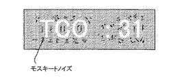
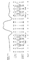
MPEG方式による圧縮画像においてモスキートノイズは非常に明るい場面や非常に暗い場面では目立ちにくく、中間の明るさのレベルから非常に明るいレベルへの画素値の変化があった場合にモスキートノイズが目立ちやすくなる。例えば図3の様に中間レベルの背景に白色のテロップが挿入されている場面などでモスキートノイズはかなり目立つ事が観察される。
【0014】
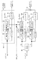
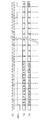
図1は本発明の実施形態の構成を示すブロック図である。各図を参照に各ブロックの処理を輝度部について説明する。
【0015】
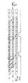
まず図5に示す入力データYinが図1の輝度部フラグ生成部101に入力される。輝度部フラグ生成部101は図2に示す構成になっており入力されたYinはエッジ検出部115に送られる。エッジ検出部115では入力信号Yinに対して図6に示す様にYinとYinを1画素ずらしたデータSFT_YINとの差分の絶対値を検出し(絶対差分値検出手段)、その絶対差分値があらかじめ設定された閾値(絶対差分値基準値)(例えばTH1が40)を超えた画素についてエッジであるとする信号EDGEを生成する(絶対差分値比較手段、画像エッジ画素検出手段)。また入力信号Yinは高レベル検出部117にも入力される。
【0016】
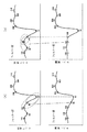
高レベル検出部117では図8(a)に示す様に入力されたYinについてあらかじめ設定された閾値(絶対値基準値)(例えばTH2が180)以上の画素を検出する(絶対値比較手段、高レベル画素検出手段)がこれがテロップの場合テロップ画素の前後は黒レベルである事が多い。この場合本発明のフィルター部104の例では図9に示す様に現画素と前後2画素及び現画素と1つ前、または1つ後の画素の平均を取る方式であるので黒レベルの値が参照されると黒レベルに近い画素値になってしまう。例として図10(a)に示す様にエッジの手前でなだらかな変化(ぼやけ)となってしまう。これを防ぐために図10(b)に示す様にテロップ画素の前後の画素はフィルター対象画素としない様にする事で余計なぼやけを回避している。この様に実際のテロップ部とその前後の画素を含めた範囲を示すフラグ2を生成する。
【0017】
また図8(b)で示す様にフラグ2が有効でテロップの終わりのエッジと次に発生するエッジの間隔がN画素(例えば5画素)未満の場合、本来テロップ部である画素が外来ノイズ等で突発的に低レベルの画素値に変化したと判断し、この場合は過敏な反応を抑えるためフラグ2は次のエッジまで有効としている。この様に生成されたフラグ2はエッジ右方向画素フィルター範囲設定部118とイネーブル信号生成部102へ送られる。
【0018】
エッジ検出部115で検出された信号EDGEはエッジ左方向画素フィルター範囲設定部116とエッジ右方向画素フィルター範囲設定部118に入力される。エッジ左方向画素フィルター範囲設定部116は入力された信号EDGEをもとに図7で示す様なタイミング図で動作する。図7(a)ではエッジ検出部115で検出された信号EDGEをもとに信号EDGEより左方向のN画素(例えば4画素)分についてフィルター対象画素としそれに対応する範囲の信号フラグ1を生成する。このフラグ1は入力データYinに対して遅れて生成されるためフィルター処理させる対象画素データも相対的にディレイさせる必要がある。このため入力データYinをディレイ部103で必要な分だけディレイ(DLY_Yin)させている。またフィルター対象範囲内でフィルター処理を可変するための画素位置(左エッジ画素側の最後画素)を示すF_EDGEを生成する。図7(b)はエッジの間隔がN画素未満(例えば5画素未満)の場合、フィルター対象画素としない様にするためフラグ1は生成しない事を示した図である。このことは外来ノイズ等で突発的に画素値が変化した場合に過敏に反応しないためと、画素値が大きく違う画素での平均化を防ぐことにもなる。
【0019】
エッジ右方向画素フィルター範囲設定部118ではエッジ検出部115から提供される信号EDGEと高レベル検出部117から提供される信号フラグ2により図11(a)の例で示す様な動作を行う。高レベル検出部117で生成されたフラグ2が発生している条件のもとでエッジ検出部115が検出した信号EDGEから右にN画素(例えば4画素)分をフィルター対象画素としそれに対応する信号フラグ3と、その対象範囲内でフィルター処理を可変するための画素位置(右エッジ画素側の最前画素)を示すB_EDGEを生成する。図11(b)の例はエッジの間隔がN画素未満(例えば5画素未満)の場合はフィルター対象画素としない様にするためフラグ3は生成しない事を示した図である。このことは外来ノイズ等で突発的に画素値が変化した場合に過敏に反応しないためと、画素値が大きく違う画素での平均化を防ぐことにもなる。
【0020】
なお、前述されたフィルター対象画素範囲設定の画素数(文中の「N画素分」)とTH1、TH2は外部より設定出来る様になっており例として挙げた「4画素」等はこれに限らず可変可能である。
【0021】
この様にモスキートノイズが発生しやすいテロップ部について、テロップの内部はフィルター処理を行わない様にするためテロップ部を示すフラグ2を生成し、テロップの前後N画素についてモスキートノイズが発生している箇所としてフィルター処理を行うためのフラグ1及びフラグ3と、フィルター処理対象範囲内でフィルター処理方法を可変するための画素位置を示すF_EDGE及びB_EDGEを生成する(ノイズ発生箇所特定手段)。
【0022】
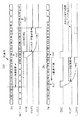
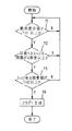
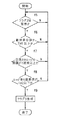
フラグ1およびフラグ3の生成フローを図12および図13に示す。図12よりフラグ1は、ステップf1で入力データと1画素ディレイしたデータの絶対差分値があらかじめ設定された閾値(TH1)以上かを判断する。TH1以上であるならステップf2で現在のエッジとこれより前のエッジの間隔が4画素以上あるかを判断する。4画素以上であるならステップf3でエッジの画素値があらかじめ設定された閾値(TH2)以上かを判断する。TH2以上であるならステップf4でフラグ1を生成し終了する。また図13よりフラグ3は、ステップf5にて高レベル検出部117で生成されたフラグ2が有効か否かを判断する。有効であるならステップf6でデータの絶対差分値がTH1以上かを判断する。TH1以上であるならステップf7で現在のエッジとこれより後に発生するエッジの間隔が4画素以上であるかを判断する。4画素以上であるならステップf8で現エッジの後の画素値がTH2以下かを判断する。TH2以下であるならステップf9でフラグ3を生成し終了する。
【0023】
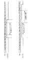
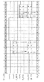
次にイネーブル信号生成部102について説明する。高レベル検出部117およびエッジ左方向画素フィルター範囲設定部116、エッジ右方向画素フィルター範囲設定部118で生成されたフラグ1、フラグ2、フラグ3および左方向のフィルター対象画素の右端を示すF_EDGEと右方向のフィルター対象画素の左端を示すB_EDGEとがイネーブル信号生成部102に入力される。イネーブル信号生成部102では上記フラグをもとに図14に示す様にEN_P(0)とEN_P(1)を生成する。3タップのフィルターを行う範囲を示すEN_P(0)はフラグ1がHでF_EDGEがLのとき有効となる。またフラグ3がHの期間も有効となる。2タップのフィルターを行う範囲を示すEN_P(1)はフラグ1がHでF_EDGEがHのとき有効となる。またフラグ3がHでB_EDGEもHのときも有効となる。このEN_P(0)とEN_P(1)から状態「0」、「1」、「2」、「3」をデコードしフィルター部104でフィルター制御を行うEN_Pを生成する。またEN_Pは外部からも制御可能であり、例えば他のノイズ軽減回路からの情報(ENP_CTL)により現在の画質が高画質と判断された場合はEN_Pを「0」とする。イネーブル生成部102で生成されたEN_Pはフィルター部104に入力される。
【0024】
フィルター部104では入力されたEN_Pの状態によりディレイ部103でディレイされた輝度データに対して、「0」はフィルター処理を行わない画素に対応させる。「1」は図9に示す3タップのフィルター処理を行う画素に対応させる。「2」は図9の2tap_aの処理で現画素(左エッジ画素側の最後画素)と1つ前の画素の2タップフィルター処理を行う画素に対応させる。「3」は図9の2tap_bの処理で現画素(右エッジ画素側の最前画素)と1つ後の画素の2タップフィルター処理を行う画素に対応させる(フィルター処理手段)。
【0025】
以上は輝度データについての動作説明であるが色差データについても基本的な動作は同じであり図5に示すCinがCb/Cr分離部113でCbデータとCrデータに分離されCbデータはCb部フラグ生成部105とディレイ部107に入力される。その後の動作は輝度部と同じである。またCr部の処理はCb部の処理と同じで色差データミックス部114にてフィルター処理を施した色差データをミックスする。
【0026】
この様に本発明では復号されたデータに対してモスキートノイズが目立ちやすい箇所にのみフィルター処理を行うので本来高周波成分が多い画素については余計なフィルター処理は行われないので全体になまった様な画像になることはない。
【0027】
また復号されたデータの画素値のみでノイズ検出およびノイズ軽減を行うため大規模なメモリーを必要とせず、単独でかつ簡単な回路が構成できる。
【0028】
また本発明は水平方向の処理について説明してきたがラインメモリーを数個持つことにより垂直方向の処理が可能となる。また垂直方向の処理も基本的に同じであり数ライン分のデータをラインメモリーに蓄え、同じ垂直方向の画素値を参照してエッジを検出後、前後N画素についてフィルター処理を施すことで更なるモスキートノイズの軽減が可能となる。
【0029】
【発明の効果】
以上のように、本発明によれば、伝送のビットレートが不足した場合に発生するモスキートノイズについて入力される画素データのみからモスキートノイズの発生する箇所が特定でき、フィルター処理を行う画素についてもフィルター処理方法を画素によって変えフィルター処理後の画質の低下を防ぐ様にしている。また突発性のエラーで画素値が大きく変わるような箇所についても閾値を設け、過敏な反応を防ぎ余計なフィルター処理がかからない様にしている。また前記してきたTH1、TH2、N画素の設定は外部より可変可能であり、状況に応じて値を変えることでより適切なノイズ軽減が出来る。これによって、大規模なメモリーを必要とせず、単独でかつ簡単な回路が構成でき画質の劣化を極力抑えモスキートノイズを軽減する事が可能となる。
【図面の簡単な説明】
【図1】本発明の全体ブロック図である。
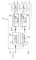
【図2】本発明の適用される輝度データ処理部のブロック図である。
【図3】モスキートノイズの発生例の図である。
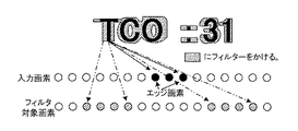
【図4】フィルター処理を施す画素の例を示した図である。
【図5】本発明に入力される画素データの例を示した図である。
【図6】入力画素データからエッジを検出するタイミング図である。
【図7】画素の高レベル(例えばテロップ)の前方向のフィルター対象画素を設定するためのタイミング図である。
【図8】画素の高レベル(例えばテロップ)を検出するためのタイミング図である。
【図9】一例のフィルター部構成図である。
【図10】フィルターの処理例を示した図である。
【図11】画素の高レベル(例えばテロップ)の後方向のフィルター対象画素を設定するためのタイミング図である。
【図12】画素の高レベル(例えばテロップ)の前方向のフィルター対象画素を設定するためのフローチャートである。
【図13】画素の高レベル(例えばテロップ)の後方向のフィルター対象画素を設定するためのフローチャートである。
【図14】輝度データについてフィルター処理を行う場合のタイミング図である。
【符号の説明】
100 輝度データ処理部
101 輝度部フラグ生成部
102 輝度部イネーブル信号生成部
103 輝度データディレイ部
104 輝度データ用フィルター部
105 Cb部フラグ生成部
106 Cb部イネーブル信号生成部
107 Cbデータディレイ部
108 Cbデータ用フィルター部
109 Cr部フラグ生成部部
110 Cr部イネーブル信号生成部
111 Crデータディレイ部
112 Crデータ用フィルター部
113 Cb/Cr分離部
114 色差データミックス部
115 輝度データエッジ検出部
116 エッジ左方向画素フィルター範囲設定部
117 高レベル検出部
118 エッジ右方向画素フィルター範囲設定部[0001]
TECHNICAL FIELD OF THE INVENTION
The present invention relates to a digital image signal processing apparatus having a function of reducing noise generated when an image compressed and encoded by the Moving Picture Coding Experts Group (MPEG) method or the like is reproduced.
[0002]
[Prior art]
Generally, when the transmission bit rate is insufficient in the MPEG system used for compressing digital image data, the image data is compressed by removing high-frequency components. When the compressed data is decompressed, noise called mosquito noise is generated at the edge of the image because high-frequency components have been deleted. Mosquito noise (also referred to as ringing noise) is noise that flickers as if a mosquito is flying at the edge of an image. This noise is more likely to occur as the transmission bit rate decreases (compression rate increases). Therefore, as a method of reducing this noise, for example, a method of increasing the transmission bit rate, a method of reducing high-frequency components during image compression (applying a low-pass filter), or a quantization scale used for encoding is used. A method of detecting encoding noise based on orthogonal transform coefficients, encoding information such as a motion vector, or a DCT coefficient, a quantization scale, and a motion vector extracted from encoded data and performing a filtering process is considered. Can be
[0003]
For each method, increasing the transmission bit rate is not efficient except in certain applications due to system limitations.
A method of compressing an image by reducing high-frequency components at the time of image compression is disclosed in, for example, JP-A-2001-231038. In this conventional example, an input video signal is processed for each divided block to create an arbitrary parameter, and the characteristics of the low-pass filter are controlled using the parameter. This control is a method that is optimally controlled according to the control of the screen and reduces obstacles such as mosquito noise.
A method of performing filtering by detecting encoding noise using encoded information is disclosed in, for example, Japanese Patent Application Laid-Open No. 7-203442. In this conventional example, a motion vector and class information indicating the reliability of the motion vector are transmitted together with transmission data from block information corresponding to the current frame of the previous frame at the time of encoding, and noise having no frame correlation is determined based on this information at the time of decoding. This is a method of controlling a recursive filter using a frame memory for reducing noise to reduce noise.
In the conventional example disclosed in Japanese Patent Application Laid-Open No. 2001-204029, a motion vector or the like for each block is extracted from the code data, and a reference area of each block is obtained from the extracted motion vector. In this method, a coding noise to be reduced is detected based on the distribution of each frequency component of the orthogonal transform coefficient in the block, and a filtering process is performed to reduce the noise.
[0004]
[Problems to be solved by the invention]
However, in the conventional technique, for example, in a method of compressing an image by reducing high-frequency components (by applying a low-pass filter), the characteristics of the low-pass filter can be optimally controlled according to the screen, and under some conditions, the entire screen may be controlled. Is subject to low-pass filter processing, resulting in an overall blurred image.
Also, in the method of performing a filtering process by detecting coding noise using coding information, in the case of Japanese Patent Application Laid-Open No. 7-203442, since a coding device and a decoding device need to be processed in conjunction, a specific If it is not a system, the effect of noise reduction cannot be obtained. In addition, since the filter is a recursive filter using a frame memory, a frame memory is required and the cost increases. In the case of Japanese Patent Application Laid-Open No. 2001-204029, a processing method differs depending on whether a macroblock is intra-frame coded (intra coded) or inter-frame coded (non-intra coded), so a frame memory is required. There is also the problem that the cost increases.
[0005]
The present invention has been made in view of such a situation, and an object of the present invention is to provide a digital image signal processing device that reduces mosquito noise in image compression encoding with a simple and inexpensive circuit configuration.
[0006]
[Means for Solving the Problems]
In order to solve the above-mentioned problems, a digital image signal processing device according to the present invention employs the following means.
[0007]
That is, the digital image signal processing device of the present invention is a digital image signal processing device having a function of reducing noise of a digital reproduced image, and includes a noise specifying a place where noise occurs based on a pixel value of digital image data. It is characterized by comprising: an occurrence location identification unit; and a filter processing unit that performs filter processing for reducing noise at the noise occurrence location identified by the noise occurrence location identification unit.
[0008]
Further, in the digital image signal processing apparatus according to the present invention, the noise occurrence location specifying means may include an absolute difference value detecting unit that detects an absolute difference value between one pixel value of the digital image data and adjacent preceding / next pixel values. Means, an absolute difference value comparing means for comparing the absolute difference value detected by the absolute difference value detecting means with a predetermined absolute difference value reference value, and an edge pixel of the image based on the result of the comparison by the absolute difference value comparing means. Image edge pixel detecting means for detecting the absolute value of the digital image data, absolute value comparing means for comparing the absolute value of the pixel value of the digital image data with a predetermined absolute value reference value, and high level based on the result of comparison by the absolute value comparing means. High-level pixel detection means for detecting pixels; noise is generated from a predetermined number of pixels from both edge pixels of the high-level pixel detected by the high-level pixel detection means toward the low-level pixel side. Characterized in that it is a means for specifying as a portion of.
[0009]
Further, the digital image signal processing apparatus according to the present invention is characterized in that a predetermined number of pixels are not subjected to a filtering process from both end edge pixels of the high-level pixel detected by the high-level pixel detection means toward the low-level pixel side.
[0010]
Further, the digital image signal processing device of the present invention, when less than a predetermined number of pixels from the edge pixels at both ends of the high-level pixel detected by the high-level pixel detection means to the next edge pixel toward the low-level pixel side, It is characterized in that no filtering is performed between pixels.
[0011]
Further, in the digital image signal processing device of the present invention, the filter processing means may include a process of averaging a pixel value to be subjected to the filter process and a pixel value of two pixels before and after the pixel, and a pixel to be subjected to the filter process being a left edge pixel of both edge pixels. The process of averaging the pixel value of the pixel to be filtered when it is the last pixel on the side and the pixel value of the previous pixel of the pixel and the filtering process when the pixel to be filtered is the foremost pixel on the right edge pixel side of both end edge pixels , And a process of averaging the pixel values of the pixel after the pixel and the pixel after the pixel.
[0012]
Further, the digital image signal processing device of the present invention is characterized in that the permission / non-permission of the filter processing can be commanded by an external signal.
[0013]
BEST MODE FOR CARRYING OUT THE INVENTION
An embodiment of a digital image signal processing device according to the present invention will be described below with reference to the drawings.
Mosquito noise in an MPEG-compressed image is less noticeable in very bright or very dark scenes, and becomes more noticeable when there is a change in pixel value from an intermediate brightness level to a very bright level. . For example, it is observed that mosquito noise is considerably conspicuous in a scene where a white telop is inserted in the middle level background as shown in FIG.
[0014]
FIG. 1 is a block diagram showing the configuration of the embodiment of the present invention. The processing of each block will be described with reference to each drawing for the luminance section.
[0015]
First, input data Yin shown in FIG. 5 is input to the luminance part
[0016]
As shown in FIG. 8A, the high-
[0017]
As shown in FIG. 8B, when the
[0018]
The signal EDGE detected by the
[0019]
The edge right pixel filter
[0020]
Note that the number of pixels (“N pixels” in the text) and TH1 and TH2 in the above-described filter target pixel range setting can be set from outside, and “4 pixels” and the like cited as an example are not limited thereto. It is variable.
[0021]
For a telop portion where mosquito noise is likely to occur in this way, a
[0022]
FIGS. 12 and 13 show a flow of generating the
[0023]
Next, the enable signal generator 102 will be described. The
[0024]
In the
[0025]
The above is the description of the operation for the luminance data, but the basic operation is the same for the color difference data. Cin shown in FIG. 5 is separated into Cb data and Cr data by the Cb /
[0026]
As described above, according to the present invention, the filtering process is performed only on the portion where mosquito noise is conspicuous on the decoded data. It will not be.
[0027]
Further, since noise detection and noise reduction are performed using only the pixel values of the decoded data, a large-scale memory is not required, and a simple and simple circuit can be configured.
[0028]
Although the present invention has been described with respect to the processing in the horizontal direction, the processing in the vertical direction becomes possible by having several line memories. The processing in the vertical direction is basically the same. Data for several lines is stored in the line memory, and an edge is detected by referring to the same pixel value in the vertical direction. Mosquito noise can be reduced.
[0029]
【The invention's effect】
As described above, according to the present invention, the location where mosquito noise occurs can be specified only from the input pixel data for the mosquito noise generated when the transmission bit rate is insufficient, and the filtering process is also performed on the pixels for which the filtering process is performed. The processing method is changed depending on the pixel to prevent the image quality after the filter processing from being deteriorated. Also, a threshold value is set for a portion where the pixel value greatly changes due to a sudden error, so that an excessive response is prevented and unnecessary filtering is not performed. The above-described settings of TH1, TH2, and N pixels can be changed externally, and more appropriate noise reduction can be achieved by changing the values according to the situation. As a result, a large-scale memory is not required, a simple and simple circuit can be formed, and deterioration of image quality can be suppressed as much as possible to reduce mosquito noise.
[Brief description of the drawings]
FIG. 1 is an overall block diagram of the present invention.
FIG. 2 is a block diagram of a luminance data processing unit to which the present invention is applied;
FIG. 3 is a diagram illustrating an example of occurrence of mosquito noise.
FIG. 4 is a diagram illustrating an example of a pixel on which a filtering process is performed;
FIG. 5 is a diagram showing an example of pixel data input to the present invention.
FIG. 6 is a timing chart for detecting an edge from input pixel data.
FIG. 7 is a timing chart for setting a high-level (for example, a telop) filter target pixel in the forward direction of a pixel;
FIG. 8 is a timing chart for detecting a high level (for example, a telop) of a pixel;
FIG. 9 is a configuration diagram of an example of a filter unit.
FIG. 10 is a diagram illustrating a processing example of a filter.
FIG. 11 is a timing chart for setting a pixel to be filtered in a backward direction of a high level (for example, a telop) of a pixel.
FIG. 12 is a flowchart for setting a high-level (for example, telop) filter target pixel in the forward direction of a pixel;
FIG. 13 is a flowchart for setting a pixel to be filtered in the backward direction of a high level (for example, a telop) of a pixel.
FIG. 14 is a timing chart when a filtering process is performed on luminance data.
[Explanation of symbols]
Claims (6)
ディジタル画像データの画素値に基づいてノイズが発生する箇所を特定するノイズ発生箇所特定手段と、ノイズ発生箇所特定手段で特定されたノイズ発生箇所にノイズを軽減するフィルター処理をするフィルター処理手段とを備えることを特徴とするディジタル画像信号処理装置。A digital image signal processing device having a function of reducing noise of a digital reproduced image,
Noise generation location specifying means for specifying a location where noise is generated based on the pixel value of the digital image data; A digital image signal processing device comprising:
Priority Applications (1)
| Application Number | Priority Date | Filing Date | Title |
|---|---|---|---|
| JP2002198910A JP2004040732A (en) | 2002-07-08 | 2002-07-08 | Digital image signal processing device |
Applications Claiming Priority (1)
| Application Number | Priority Date | Filing Date | Title |
|---|---|---|---|
| JP2002198910A JP2004040732A (en) | 2002-07-08 | 2002-07-08 | Digital image signal processing device |
Publications (1)
| Publication Number | Publication Date |
|---|---|
| JP2004040732A true JP2004040732A (en) | 2004-02-05 |
Family
ID=31706234
Family Applications (1)
| Application Number | Title | Priority Date | Filing Date |
|---|---|---|---|
| JP2002198910A Pending JP2004040732A (en) | 2002-07-08 | 2002-07-08 | Digital image signal processing device |
Country Status (1)
| Country | Link |
|---|---|
| JP (1) | JP2004040732A (en) |
-
2002
- 2002-07-08 JP JP2002198910A patent/JP2004040732A/en active Pending
Similar Documents
| Publication | Publication Date | Title |
|---|---|---|
| US7620261B2 (en) | Edge adaptive filtering system for reducing artifacts and method | |
| US8218083B2 (en) | Noise reducer, noise reducing method, and video signal display apparatus that distinguishes between motion and noise | |
| US20120262598A1 (en) | Image signal processing apparatus | |
| KR100621005B1 (en) | Image Error Recovery Device and Method | |
| US7031388B2 (en) | System for and method of sharpness enhancement for coded digital video | |
| WO2007093942A2 (en) | Reduction of compression artefacts in displayed images, analysis of encoding parameters | |
| CN102119400B (en) | Dark noise artifact detection method and device | |
| EP1352515B1 (en) | Apparatus and method for providing a usefulness metric based on coding information for video enhancement | |
| CN101207769B (en) | Method and system for providing video interface between video disc player and TV | |
| US8135231B2 (en) | Image processing method and device for performing mosquito noise reduction | |
| JPH089370A (en) | Image encoding method | |
| KR20180101607A (en) | An encoding apparatus including a video switching apparatus and an encoding method including a video switching detecting method | |
| JP2004040732A (en) | Digital image signal processing device | |
| JP4500112B2 (en) | Image feature amount detection device, image quality improvement device, display device, and receiver | |
| JP3256605B2 (en) | Image signal receiving device | |
| JP3202270B2 (en) | Video encoding device | |
| JPH1056646A (en) | Video signal decoding device | |
| JP3958281B2 (en) | Video encoding device | |
| JP4186769B2 (en) | GOP cycle detector | |
| KR100261109B1 (en) | Luminance signal compression encoding device that can improve image quality | |
| JP3371773B2 (en) | Signal processing method and signal reproducing device | |
| WO2010021039A1 (en) | Image processing device, image processing method, and image processing program | |
| JP2006121131A (en) | Noise detector and noise detecting program | |
| JP2005079617A (en) | Device and method for reducing block distortion and program for block distortion reduction | |
| JP2002010268A (en) | Image encoding apparatus and image encoding method |
Legal Events
| Date | Code | Title | Description |
|---|---|---|---|
| A621 | Written request for application examination |
Free format text: JAPANESE INTERMEDIATE CODE: A621 Effective date: 20050525 |
|
| A977 | Report on retrieval |
Free format text: JAPANESE INTERMEDIATE CODE: A971007 Effective date: 20070426 |
|
| A131 | Notification of reasons for refusal |
Free format text: JAPANESE INTERMEDIATE CODE: A131 Effective date: 20070508 |
|
| A521 | Written amendment |
Free format text: JAPANESE INTERMEDIATE CODE: A523 Effective date: 20070627 |
|
| A131 | Notification of reasons for refusal |
Free format text: JAPANESE INTERMEDIATE CODE: A131 Effective date: 20080527 |
|
| A02 | Decision of refusal |
Free format text: JAPANESE INTERMEDIATE CODE: A02 Effective date: 20080930 |