JP2004031918A - Semiconductor device - Google Patents
Semiconductor device Download PDFInfo
- Publication number
- JP2004031918A JP2004031918A JP2003087857A JP2003087857A JP2004031918A JP 2004031918 A JP2004031918 A JP 2004031918A JP 2003087857 A JP2003087857 A JP 2003087857A JP 2003087857 A JP2003087857 A JP 2003087857A JP 2004031918 A JP2004031918 A JP 2004031918A
- Authority
- JP
- Japan
- Prior art keywords
- layer
- film
- wiring
- insulating
- insulating layer
- Prior art date
- Legal status (The legal status is an assumption and is not a legal conclusion. Google has not performed a legal analysis and makes no representation as to the accuracy of the status listed.)
- Pending
Links
Images


Classifications
-
- H—ELECTRICITY
- H01—ELECTRIC ELEMENTS
- H01L—SEMICONDUCTOR DEVICES NOT COVERED BY CLASS H10
- H01L2224/00—Indexing scheme for arrangements for connecting or disconnecting semiconductor or solid-state bodies and methods related thereto as covered by H01L24/00
- H01L2224/01—Means for bonding being attached to, or being formed on, the surface to be connected, e.g. chip-to-package, die-attach, "first-level" interconnects; Manufacturing methods related thereto
- H01L2224/42—Wire connectors; Manufacturing methods related thereto
- H01L2224/44—Structure, shape, material or disposition of the wire connectors prior to the connecting process
- H01L2224/45—Structure, shape, material or disposition of the wire connectors prior to the connecting process of an individual wire connector
- H01L2224/45001—Core members of the connector
- H01L2224/45099—Material
- H01L2224/451—Material with a principal constituent of the material being a metal or a metalloid, e.g. boron (B), silicon (Si), germanium (Ge), arsenic (As), antimony (Sb), tellurium (Te) and polonium (Po), and alloys thereof
- H01L2224/45138—Material with a principal constituent of the material being a metal or a metalloid, e.g. boron (B), silicon (Si), germanium (Ge), arsenic (As), antimony (Sb), tellurium (Te) and polonium (Po), and alloys thereof the principal constituent melting at a temperature of greater than or equal to 950°C and less than 1550°C
- H01L2224/45144—Gold (Au) as principal constituent
-
- H—ELECTRICITY
- H01—ELECTRIC ELEMENTS
- H01L—SEMICONDUCTOR DEVICES NOT COVERED BY CLASS H10
- H01L2224/00—Indexing scheme for arrangements for connecting or disconnecting semiconductor or solid-state bodies and methods related thereto as covered by H01L24/00
- H01L2224/01—Means for bonding being attached to, or being formed on, the surface to be connected, e.g. chip-to-package, die-attach, "first-level" interconnects; Manufacturing methods related thereto
- H01L2224/42—Wire connectors; Manufacturing methods related thereto
- H01L2224/47—Structure, shape, material or disposition of the wire connectors after the connecting process
- H01L2224/48—Structure, shape, material or disposition of the wire connectors after the connecting process of an individual wire connector
- H01L2224/4805—Shape
- H01L2224/4809—Loop shape
- H01L2224/48091—Arched
-
- H—ELECTRICITY
- H01—ELECTRIC ELEMENTS
- H01L—SEMICONDUCTOR DEVICES NOT COVERED BY CLASS H10
- H01L2224/00—Indexing scheme for arrangements for connecting or disconnecting semiconductor or solid-state bodies and methods related thereto as covered by H01L24/00
- H01L2224/01—Means for bonding being attached to, or being formed on, the surface to be connected, e.g. chip-to-package, die-attach, "first-level" interconnects; Manufacturing methods related thereto
- H01L2224/42—Wire connectors; Manufacturing methods related thereto
- H01L2224/47—Structure, shape, material or disposition of the wire connectors after the connecting process
- H01L2224/48—Structure, shape, material or disposition of the wire connectors after the connecting process of an individual wire connector
- H01L2224/481—Disposition
- H01L2224/48151—Connecting between a semiconductor or solid-state body and an item not being a semiconductor or solid-state body, e.g. chip-to-substrate, chip-to-passive
- H01L2224/48221—Connecting between a semiconductor or solid-state body and an item not being a semiconductor or solid-state body, e.g. chip-to-substrate, chip-to-passive the body and the item being stacked
- H01L2224/48245—Connecting between a semiconductor or solid-state body and an item not being a semiconductor or solid-state body, e.g. chip-to-substrate, chip-to-passive the body and the item being stacked the item being metallic
- H01L2224/48247—Connecting between a semiconductor or solid-state body and an item not being a semiconductor or solid-state body, e.g. chip-to-substrate, chip-to-passive the body and the item being stacked the item being metallic connecting the wire to a bond pad of the item
-
- H—ELECTRICITY
- H01—ELECTRIC ELEMENTS
- H01L—SEMICONDUCTOR DEVICES NOT COVERED BY CLASS H10
- H01L2924/00—Indexing scheme for arrangements or methods for connecting or disconnecting semiconductor or solid-state bodies as covered by H01L24/00
- H01L2924/0001—Technical content checked by a classifier
- H01L2924/00011—Not relevant to the scope of the group, the symbol of which is combined with the symbol of this group
-
- H—ELECTRICITY
- H01—ELECTRIC ELEMENTS
- H01L—SEMICONDUCTOR DEVICES NOT COVERED BY CLASS H10
- H01L2924/00—Indexing scheme for arrangements or methods for connecting or disconnecting semiconductor or solid-state bodies as covered by H01L24/00
- H01L2924/01—Chemical elements
- H01L2924/01015—Phosphorus [P]
-
- H—ELECTRICITY
- H01—ELECTRIC ELEMENTS
- H01L—SEMICONDUCTOR DEVICES NOT COVERED BY CLASS H10
- H01L2924/00—Indexing scheme for arrangements or methods for connecting or disconnecting semiconductor or solid-state bodies as covered by H01L24/00
- H01L2924/01—Chemical elements
- H01L2924/01019—Potassium [K]
-
- H—ELECTRICITY
- H01—ELECTRIC ELEMENTS
- H01L—SEMICONDUCTOR DEVICES NOT COVERED BY CLASS H10
- H01L2924/00—Indexing scheme for arrangements or methods for connecting or disconnecting semiconductor or solid-state bodies as covered by H01L24/00
- H01L2924/01—Chemical elements
- H01L2924/01078—Platinum [Pt]
-
- H—ELECTRICITY
- H01—ELECTRIC ELEMENTS
- H01L—SEMICONDUCTOR DEVICES NOT COVERED BY CLASS H10
- H01L2924/00—Indexing scheme for arrangements or methods for connecting or disconnecting semiconductor or solid-state bodies as covered by H01L24/00
- H01L2924/10—Details of semiconductor or other solid state devices to be connected
- H01L2924/102—Material of the semiconductor or solid state bodies
- H01L2924/1025—Semiconducting materials
- H01L2924/10251—Elemental semiconductors, i.e. Group IV
- H01L2924/10253—Silicon [Si]
-
- H—ELECTRICITY
- H01—ELECTRIC ELEMENTS
- H01L—SEMICONDUCTOR DEVICES NOT COVERED BY CLASS H10
- H01L2924/00—Indexing scheme for arrangements or methods for connecting or disconnecting semiconductor or solid-state bodies as covered by H01L24/00
- H01L2924/10—Details of semiconductor or other solid state devices to be connected
- H01L2924/11—Device type
- H01L2924/13—Discrete devices, e.g. 3 terminal devices
- H01L2924/1304—Transistor
- H01L2924/1306—Field-effect transistor [FET]
- H01L2924/13091—Metal-Oxide-Semiconductor Field-Effect Transistor [MOSFET]
-
- H—ELECTRICITY
- H01—ELECTRIC ELEMENTS
- H01L—SEMICONDUCTOR DEVICES NOT COVERED BY CLASS H10
- H01L2924/00—Indexing scheme for arrangements or methods for connecting or disconnecting semiconductor or solid-state bodies as covered by H01L24/00
- H01L2924/15—Details of package parts other than the semiconductor or other solid state devices to be connected
- H01L2924/181—Encapsulation
-
- H—ELECTRICITY
- H01—ELECTRIC ELEMENTS
- H01L—SEMICONDUCTOR DEVICES NOT COVERED BY CLASS H10
- H01L2924/00—Indexing scheme for arrangements or methods for connecting or disconnecting semiconductor or solid-state bodies as covered by H01L24/00
- H01L2924/30—Technical effects
- H01L2924/301—Electrical effects
- H01L2924/3025—Electromagnetic shielding
Abstract
Description
【0001】
【発明の属する技術分野】
本発明は、低誘電率特性を有する絶縁膜を層間絶縁膜に用いることで、信号配線遅延を低減し、これにより素子性能の向上を図った半導体装置に関する。
【0002】
【従来の技術】
半導体素子の高集積化とチップサイズの縮小に伴い、配線の微細化、狭ピッチ化及び多層化が進められている。これに伴って、信号が配線を伝播するときの遅れ時間、即ち配線遅延が増加する傾向にあり、半導体素子を用いた電子機器を使用するに際して大きな問題となっている。
一般に、配線を伝播する信号の速度は配線抵抗(R)と配線間容量(C)の積(RC)によって決まるため、配線抵抗を下げること、又は配線間容量を小さくすること、即ち層間絶縁膜の低誘電率化を行うことが配線遅延を低減するために必要である。
【0003】
配線抵抗を下げることに対して、高性能な半導体素子では、配線材料をアルミニウムから銅に替えることが進められており、特に銅配線を層間絶縁膜層に埋め込むダマシン構造のプロセス適用が盛んに行われている。
【0004】
また、層間絶縁膜の低誘電率化に対しては、従来、半導体装置の層間絶縁膜にはCVD(化学蒸着:Chemical Vapor Deposition)法を用いて成膜されたシリコン酸化膜(SiO2:比誘電率4.0程度)やシリコン窒化膜(Si−N:比誘電率7.0程度)等の無機系材料が使用されていた。そして、従来のプロセスを踏襲できる低誘電率材料として、最近ではフッ素添加シリコン酸化膜(Si−O−F:比誘電率3.6程度)の採用が相次いでいる。
【0005】
しかしながら、フッ素添加シリコン酸化膜の誘電率は比較的高く、これを層間絶縁膜として使用した場合には層間容量を低減する効果が十分でないため、配線プロセス90nmノード世代以降の半導体装置ではさらに低い誘電率を有する材料が必要とされている。
【0006】
比誘電率が3.5を下回る特性を有する層間絶縁膜材料として、種々の材料が提案されており、大きく区分すると、基板に塗布した後に加熱により膜を形成するいわゆるスピンオングラス材料や同様に成膜形成する有機系材料と、CVD法を用いて成膜形成する手法が検討も検討されている。
【0007】
スピンオングラス材料としては、シルセスキオキサン水素(Hydrogen Silsesquioxane)化合物又はシルセスキオキサンメチル(Methyl Silsesquioxane)化合物を含む材料が挙げられる。シルセスキオキサン水素化合物又はシルセスキオキサンメチル化合物を主成分として含む材料が好ましい。なお、本明細書において主成分とは、最も配合比(モル比)の高い成分をいう。
【0008】
シルセスキオキサン水素化合物を主成分とする塗布溶液は、一般式(HSiO3/2)nで表される化合物をメチルイソブチルケトンなどの溶媒に溶解させたものである。この溶液を基板に塗布し、100〜250℃程度の温度で中間加熱したのち、窒素雰囲気中などの不活性雰囲気内にて350〜450℃の温度で加熱することにより、Si−O−Siの結合がラダー構造的に形成され、最終的にSiOを主成分とする絶縁膜が形成される。
【0009】
シルセスキオキサンメチル化合物を主成分とする塗布溶液は、一般式(CH3SiO3/2)nで表される化合物をメチルイソブチルケトンなどの溶媒に溶解させたものである。この溶液を基板に塗布し、100〜250℃程度の温度で中間加熱したのち、窒素雰囲気中などの不活性雰囲気内にて350〜450℃の温度で加熱することにより、Si−O−Siの結合がラダー構造的に形成され、最終的にSiOを主成分とする絶縁膜が形成される。
【0010】
有機絶縁膜材料としては、炭化水素系樹脂であるポリイミド、ポリパラキシリレン、ポリアリーレンエーテル、ポリアリーレン、ベンズシクロブテン、ポリナフタレン等の高分子材料が知られている。これらの材料は、炭素原子を含有することで膜の密度を低減させ、また分子(モノマ)自身の分極率を小さくすることで低誘電率を達成している。
【0011】
上述のようなスピンオングラス膜、有機膜、CVD膜といった層間絶縁膜の比誘電率をさらに低減する手法として、膜中に微小空孔を形成して多孔質膜とすることが知られている。上記の材料やプロセスに関して、「International Technology Roadmap for Semiconductors」(1999年編)第163〜186頁、特開2000−340569号公報、特開2001−274239号公報に開示されている。
【0012】
しかしながら、上述した従来技術において、比誘電率が3.5を下回る特性を有する層間絶縁膜では、CVD成膜のシリコン酸化膜やシリコン窒化膜に比べて、絶縁膜の硬度や弾性率といった機械的強度が本質的に低いという問題点を抱えている。
【0013】
このような絶縁膜において、さらに比誘電率を低減するため膜中に微小空孔を形成して多孔質化することは、機械的な強度をさらに劣化させる方向にあって、現実的ではないとされていた。
【0014】
絶縁膜の比誘電率を下げる手段として、ポリイミドなどの絶縁性有機ポリマを用いることがある。有機ポリマはその比誘電率が4未満であるので好都合であるが、無機膜に比べて物理的に機械的強度が低く、また吸湿性や透湿性が高いという欠点がある。また、層間絶縁膜として利用する場合、素子構造の機械的強度の低下及び吸湿水分による配線の腐食等、素子の信頼性に問題が生じる。
【非特許文献1】
「International Technology Roadmap for Semiconductors」(1999年編)第163〜186頁
【特許文献1】
特開2000−340569号公報
【特許文献2】
特開2001−274239号公報
【0015】
【発明が解決しようとする課題】
そこで、特に、配線抵抗を下げた銅配線を層間絶縁膜層に埋め込むダマシン構造を適用した多層配線半導体素子において、素子構造の機械的強度の低下を抑えながら、層間絶縁膜全体の誘電率を下げる方法を検討した。
【0016】
本願発明は上記した技術的背景のもとに、上記の如き誘電率の低い膜と誘電率の高い膜との積層構造にし、かつ、各々の材料の組合せや構造の最適化を図ることによって、絶縁膜自身の電気的な特性と機械的な特性との両立を実現する方法を提案するものである。
【0017】
特に、配線抵抗を下げた銅配線を層間絶縁膜層に埋め込むダマシン構造を適用した積層構造の半導体装置において、層間絶縁膜の機械的強度の低下を抑制しつつ、配線を伝播する信号の遅延を極力低減させた高信頼で高性能な特性を有する半導体装置を可能とした。
【0018】
【課題を解決するための手段】
本発明の半導体装置は、トランジスタ素子や半導体回路部が形成された基板上に、第1の絶縁層と、第2の絶縁層と、第3の絶縁層と、その3層を貫通するように形成された導体配線を備えた配線層を複数層積層して形成された半導体装置である。このとき、各配線層を構成する第1と第3の絶縁層が、シリコン炭化窒化膜、シリコン炭化物又はシリコン酸化物からなり、また、配線層のうち、下層部に位置する配線層の第2の絶縁層がシリコン酸化物を含み、上層部に位置する配線層の第2の絶縁層がフッ素添加シリコン酸化物又は炭素添加シリコン酸化物を含むようにした。
【0019】
このとき、導体配線として銅配線を構成要素とした場合、第1の絶縁膜は銅配線を埋め込むために絶縁膜を開口する際のエッチングストッパー膜となる。また、第3の絶縁層は銅配線の拡散バリア膜となる。
【0020】
従来、エッチングストッパー膜や拡散バリア膜はシリコン窒化膜が用いられており、本発明ではシリコン窒化膜より比誘電率の低いシリコン炭化窒化膜(Si−C−N:比誘電率4.6程度)、シリコン炭化物(Si−C:比誘電率4.4程度)又はシリコン酸化物からなる膜を用いるため、多層積層構造にした配線層全体においても、その比誘電率を低減できる。
【0021】
配線層のうち、上層部に位置する配線層の第2の絶縁層がシリコン酸化膜より比誘電率の小さいフッ素添加シリコン酸化膜又は炭素添加シリコン酸化膜(比誘電率2.9程度)にすることによって、配線層を構成する全ての第2の絶縁層がシリコン酸化物とした場合に比べて、配線層全体の比誘電率を低減できる。
【0022】
また、本発明の半導体装置は下層部に位置する配線層の第2の絶縁層が比誘電率3.0未満の絶縁膜材からなり、上層部に位置する配線層の第2の絶縁層がフッ素添加シリコン酸化膜又は炭素添加シリコン酸化膜からなるようにした。即ち、第2の絶縁層の構成成分が上層部に位置する配線層と下層部に位置する配線層とで異なるようにし、前者に比較して後者の絶縁膜の比誘電率が小さくなるようにした。
【0023】
また、本発明の半導体装置は、下層部に位置する配線層の第2の絶縁層が比誘電率3.0未満の特性を有し、SiOを含有する絶縁膜であって、かつ絶縁膜中に存在する微小空孔の半数以上が0.05nm以上4nm以下の直径を有するようにした。本発明では、微小空孔の主要構成が直径0.05nm以上4nm以下であることが望ましい。本発明では、膜中に微小空孔を有することで、膜の密度を低減し、単膜としての比誘電率3.0未満と小さくしたSiOを含有する絶縁膜を用いることで、多層積層構造の配線層全体ではさらに比誘電率を低減できる。
【0024】
この時、絶縁膜中に微少な空孔を形成して密度を低下させ、真空の比誘電率に近づけるという方法を用いることによって、絶縁膜の比誘電率をシリコン酸化膜の比誘電率より低下させ、特に、この微小空孔の寸法や密度を制御することによって、任意の比誘電率を有する絶縁膜を形成することができる。
【0025】
しかしながら、微小空孔の径が大きくなると絶縁膜自身の構造体としての機械的強度が低下する、又は、絶縁膜を流れるリーク電流が大きくなって絶縁膜としての特徴である絶縁耐圧が低下する等の問題も新たに生じることとなり、絶縁膜中に含有させる空孔の大きさには、細心の注意が必要である。
【0026】
そこで、本発明では、空孔径の範囲を制御することで、絶縁膜の機械的強度や絶縁耐圧の低下を抑制するようにした。このとき、微小空孔の半数以上が0.05nm以上4nm以下の径である場合に、絶縁膜の膜強度を低下させないで信頼性の高い半導体装置が可能となる。
【0027】
上記した微小空孔を有する絶縁膜は、シルセスキオキサン水素化合物又はシルセスキオキサンメチル化合物を主成分とする膜を加熱して得られるSiOを主成分とする絶縁膜で形成される。
【0028】
シルセスキオキサン水素化合物を主成分とする塗布溶液は、一般式(HSiO3/2)nで表される化合物をメチルイソブチルケトンなどの溶媒に溶解させたものである。また、シルセスキオキサンメチル化合物を主成分とする塗布溶液は、一般式(CH3SiO3/2)nで表される化合物をメチルイソブチルケトンなどの溶媒に溶解させたものである。
【0029】
これらの溶液を基板に塗布し、100〜250℃程度の温度で中間加熱したのち、窒素雰囲気中などの不活性雰囲気内にて350〜450℃の温度で加熱することにより、Si−O−Siの結合がラダー構造的に形成され、最終的にSiOを主成分とする絶縁膜が形成される。
【0030】
シルセスキオキサン水素化合物又はシルセスキオキサンメチル化合物を主成分とする膜を加熱して得られるSiOを主成分とする絶縁膜において、絶縁膜中に存在する空孔の径を制御する手法として、例えば、シルセスキオキサン(Silsesquioxane)化合物溶液にメチルイソブチルケトンなどの溶媒以外の成分を含有させ、膜中で本成分が分解した跡が空孔として形成し、成膜温度により分解挙動を変化させることで、空孔形成を制御し、空孔径範囲を選択的な範囲に収めることを可能とする手法が挙げられる。
【0031】
上記した絶縁膜形成用の溶液を塗布する方法としては、回転塗布やスリット塗布又は印刷方式が挙げられる。そして、絶縁膜はこの膜を加熱して形成されるため、高密度に微細な配線を形成した場合であってもCVD法による絶縁膜と比較して、段差の被覆性が良好であって、表面段差を解消できるという点で優位となる。
【0032】
また、Siウエハの大口径化に対して、CVD法を用いて絶縁膜を形成する場合には大型の成膜装置を必要とし、設備コストが素子コストに大きな影響をきたすことになる。これに対して、本発明では塗布・加熱方式で絶縁膜を形成するため、設備コストの大幅な低減が可能であって、製造ラインの投資コスト、さらには素子コストを抑えると言う大きな効果が期待できる。
【0033】
CVD法で絶縁膜を形成する場合は、アルキルシラン化合物、アルコキシシラン化合物を主成分としてソースガスに利用して、ECR(Electron Cyclotron Resonance)プラズマCVD法などで、最終的にSiOを主成分とする絶縁膜を形成する。
【0034】
この場合も、絶縁膜中に存在する空孔の径を制御する手法として、例えば、ソースガスとして熱分解温度の高い成分を含有させ、成膜時に350℃〜450℃の加熱により、膜中で本成分が分解した跡が空孔として形成される手法が挙げられる。
【0035】
このような手法では、熱分解温度の高い成分を種々選択することで、成膜温度により分解挙動が変化させることが可能で、これにより空孔形成を制御することで、空孔径範囲を選択的な範囲に収めることを可能とする。
【0036】
また、本発明の半導体装置では、半導体装置周辺部からの吸湿、透湿を防ぐために素子装置周辺を囲うように導体配線を形成する材料から構成された隔壁層(本発明ではガードリングと称する)を素子装置周辺に設ける。これにより、本発明によれば素子周辺や基板と層間絶縁膜の界面から層間絶縁膜内を透過してくる水分を遮蔽し、素子自体の耐湿信頼性を向上させることができる。
【0037】
【発明の実施の形態】
以下、本発明の実施の形態について図面を参照して説明する。
【0038】
(第1の実施例)
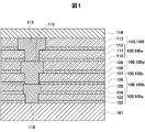
第1の実施例では、図1に示すように6層の配線層100を有するCu配線デュアルダマシン構造の6層配線半導体素子を作製した。
【0039】
一般的に良く知られた方法を用いてMOSトランジスタ等の構成素子(図示省略)を形成した半導体基板101上に、第1配線層100aの第1絶縁層となるシリコン炭化窒化膜102を40nm厚でCVD法を用いて形成した。この第1絶縁層は、配線パターンを形成する開口時にエッチングストッパー膜となる。
【0040】
次に、第1配線層100aの第2絶縁層となるシリコン酸化膜103を400nm厚でCVD法を用いて形成した。
【0041】
次に、第1配線層100aの第3絶縁層となるシリコン炭化窒化膜104を40nm厚でCVD法を用いて形成した。この膜は第2配線層100bの第1絶縁層として配線パターンを形成する開口時にエッチングストッパー膜やCu拡散バリア膜としての役目も果たす。
【0042】
次に、シリコン炭化窒化膜104に開口117を形成した。開口は、フォトレジストを用いて、周知の技術でレジストパターンを形成し、シリコン炭化窒化膜を除去できるエッチングガスを用いて、レジストをマスクにしてドライエッチング方式を用いて形成した(図2(a))。このとき、開口は第1配線層100aの配線寸法となっている。
【0043】
次に、第1配線層100a形成と同様の方法を用いて、第2配線層100bの第2絶縁層となるシリコン酸化膜105を400nm厚で、第3絶縁層となるシリコン炭化窒化膜106を40nm厚で形成した。
【0044】
次に、シリコン炭化窒化膜に開口118を形成した(図2(b))。開口は、フォトレジストを用いて、周知の技術でレジストパターンを形成し、シリコン炭化窒化膜を除去できるエッチングガスを用いて、レジストをマスクにしてドライエッチング方式を用いて形成した。
【0045】
次に、シリコン炭化窒化膜をマスクにしてシリコン酸化膜を除去できるCF系ガスを用いてドライエッチング方式で、シリコン酸化膜105に開口を形成し、その下部でシリコン炭化窒化膜104の開口117が露出する。
【0046】
引き続き、シリコン炭化窒化膜104の開口117をマスクに、シリコン酸化膜103に開口を形成し、その下部でシリコン炭化窒化膜102を露出させた。
【0047】
続いて、シリコン炭化窒化膜を除去できるエッチングガスに切替え、シリコン酸化膜103の開口をマスクに、シリコン炭化窒化膜102をドライエッチング除去し、半導体基板101に貫通する開口を形成した。このとき、シリコン炭化窒化膜104もエッチングされて、最上層のシリコン炭化窒化膜の開口118と同じ寸法に広がる。これにより、半導体基板101に貫通する配線溝119を形成した(図2(c))。
【0048】
次に、配線溝119内面にバリアメタル膜120を形成した後、良く知られたメッキ法を用いてCu121の充填を行った。バリアメタルは、本実施例ではTiNを用いた。
【0049】
そして、最上層であるシリコン炭化窒化膜上に存在する不要なCu膜を除去し、表面を洗浄することで、接続用プラグと配線を同時に形成した。Cu膜の除去には、砥粒としてアルミナ又はシリカを用い、Cu錯化剤、界面活性剤等の添加剤からなる研磨剤を用いた化学機械研磨法(Chemical Mechanical Polishing)を用いることが好都合である。
【0050】
この研磨工程で、最上層に当たるシリコン炭化窒化膜106も研磨除去した。これにより、Cu配線(120と121を含む)を形成したデュアルダマシン構造を作製した(図2(d))。
【0051】
続いて、同様の工程を2度行って第3配線層100c〜第6配線層100fを形成し、6層のCu配線構造を得た。このとき、絶縁層106、108、110、112は、CVD法を用いて成膜したシリコン炭化窒化膜からなり、絶縁層107、109はシリコン酸化膜からなる。また、絶縁層111、113は、フッ素添加シリコン酸化膜からなる。
【0052】
次に、最上層にシリコン窒化膜114を形成して、6層のCu配線115を備える多層配線半導体素子を作製した(図1)。
【0053】
これにより、エッチングストッパー膜や拡散バリア膜として、シリコン窒化膜より比誘電率の低いシリコン炭化窒化膜を用い、また、多層構造の上層部において、シリコン酸化膜より比誘電率の小さいフッ素添加シリコン酸化膜を用いることで、層間絶縁膜全体の誘電率を下げた高性能の半導体装置が得られた。
【0054】
(第2の実施例)
第1の実施例と同様の手法を用いて、本実施例では絶縁層107、109についてもCVD法を用いてフッ素添加シリコン酸化膜を成膜した。次に、最上層にシリコン窒化膜114を形成し、6層のCu配線115を備える多層配線半導体素子を作製した。
【0055】
これにより、エッチングストッパー膜や拡散バリア膜として、シリコン窒化膜より比誘電率の低いシリコン炭化窒化膜を用い、また、多層構造の1/3以上の上層部において、シリコン酸化膜より比誘電率の小さいフッ素添加シリコン酸化膜を用いることで、層間絶縁膜全体の誘電率を下げた高性能の半導体装置が得られた。
【0056】
(第3の実施例)
第1の実施例と同様の手法を用いて、本実施例では絶縁層102、104、106、108、110、112について、CVD法を用いてシリコン炭化膜を成膜した。次に、最上層にシリコン窒化膜114を形成し、6層のCu配線115を備える多層配線半導体素子を作製した。
【0057】
これにより、エッチングストッパー膜や拡散バリア膜として、シリコン窒化膜より比誘電率の低いシリコン炭化膜を用いることで、層間絶縁膜全体の誘電率を下げた高性能の半導体装置が得られた。
【0058】
(第4の実施例)
第2の実施例と同様の手法を用いて、本実施例では絶縁層102、104、106、108、110、112について、CVD法を用いてシリコン炭化膜を成膜した。次に、最上層にシリコン窒化膜114を形成し、6層のCu配線115を備える多層配線半導体素子を作製した。
【0059】
これにより、エッチングストッパー膜や拡散バリア膜として、シリコン窒化膜より比誘電率の低いシリコン炭化膜を用いることで、層間絶縁膜全体の誘電率を下げた高性能の半導体装置が得られた。
【0060】
(第5の実施例)
第1の実施例と同様の手法を用いて、本実施例では絶縁層111、113について、CVD法を用いて炭素添加シリコン酸化膜を成膜し、6層のCu配線115を備える多層配線半導体素子を作製した。
【0061】
これにより、多層構造の上層部において、シリコン酸化膜より比誘電率の小さい炭素添加シリコン酸化膜を用いることで、層間絶縁膜全体の誘電率を下げた高性能の半導体装置が得られた。
【0062】
(第6の実施例)
第2の実施例と同様の手法を用いて、本実施例では絶縁層107、109、111、113について、CVD法を用いて炭素添加シリコン酸化膜を成膜し、6層のCu配線115を備える多層配線半導体素子を作製した。
【0063】
また、多層構造の1/3以上の上層部において、シリコン酸化膜より比誘電率の小さい炭素添加シリコン酸化膜を用いることで、層間絶縁膜全体の誘電率を下げた高性能の半導体装置が得られた。
【0064】
(第7の実施例)
第5の実施例と同様の手法を用いて、本実施例では絶縁層102、104、106、108、110、112について、CVD法を用いてシリコン炭化膜を成膜した。次に、最上層にシリコン窒化膜114を形成し、6層のCu配線115を備える多層配線半導体素子を作製した。
【0065】
これにより、エッチングストッパー膜や拡散バリア膜として、シリコン窒化膜より比誘電率の低いシリコン炭化膜を用いることで、層間絶縁膜全体の誘電率を下げた高性能の半導体装置が得られた。
【0066】
(第8の実施例)
第6の実施例と同様の手法を用いて、本実施例では絶縁層102、104、106、108、110、112について、CVD法を用いてシリコン炭化膜を成膜した。次に、最上層にシリコン窒化膜114を形成し、6層のCu配線115を備える多層配線半導体素子を作製した。
【0067】
これにより、エッチングストッパー膜や拡散バリア膜として、シリコン窒化膜より比誘電率の低いシリコン炭化膜を用いることで、層間絶縁膜全体の誘電率を下げた高性能の半導体装置が得られた。
【0068】
(第9の実施例)
第1の実施例と同様の手法を用いて、本実施例では絶縁層103、105、107、109について、CVD法を用いて炭素添加シリコン酸化膜を成膜し、6層のCu配線115を備える多層配線半導体素子を作製した。
【0069】
これにより、多層構造の下層部において、比誘電率の低い炭素添加シリコン酸化膜を絶縁膜に用い、また、多層構造の上層部において、シリコン酸化膜より比誘電率の小さいフッ素添加シリコン酸化膜を用いることで、層間絶縁膜全体の誘電率を下げた高性能の半導体装置が得られた。
【0070】
(第10の実施例)
第2の実施例と同様の手法を用いて、本実施例では絶縁層103、105について、CVD法を用いて炭素添加シリコン酸化膜を成膜し、6層のCu配線115を備える多層配線半導体素子を作製した。
【0071】
これにより、多層構造の下層部において、比誘電率の低い炭素添加シリコン酸化膜を絶縁膜に用い、また、多層構造の1/3以上の上層部において、シリコン酸化膜より比誘電率の小さいフッ素添加シリコン酸化膜を用いることで、層間絶縁膜全体の誘電率を下げた高性能の半導体装置が得られた。
【0072】
(第11の実施例)
第3の実施例と同様の手法を用いて、本実施例では絶縁層103、105、107、109について、CVD法を用いて炭素添加シリコン酸化膜を成膜し、6層のCu配線115を備える多層配線半導体素子を作製した。
【0073】
これにより、多層構造の下層部において、比誘電率の低い炭素添加シリコン酸化膜を絶縁膜に用い、また、多層構造の上層部において、シリコン酸化膜より比誘電率の小さいフッ素添加シリコン酸化膜を用い、エッチングストッパー膜や拡散バリア膜として、シリコン窒化膜より比誘電率の低いシリコン炭化膜を用いることで、層間絶縁膜全体の誘電率を下げた高性能の半導体装置が得られた。
【0074】
(第12の実施例)
第4の実施例と同様の手法を用いて、本実施例では絶縁層103、105について、CVD法を用いて炭素添加シリコン酸化膜を成膜し、6層のCu配線115を備える多層配線半導体素子を作製した。
【0075】
これにより、多層構造の下層部において、比誘電率の低い炭素添加シリコン酸化膜を絶縁膜に用い、また、多層構造の1/3以上の上層部において、シリコン酸化膜より比誘電率の小さいフッ素添加シリコン酸化膜を用い、エッチングストッパー膜や拡散バリア膜として、シリコン窒化膜より比誘電率の低いシリコン炭化膜を用いることで、層間絶縁膜全体の誘電率を下げた高性能の半導体装置が得られた。
【0076】
(第13の実施例)
第1の実施例と同様の手法を用いて、本実施例では、絶縁層103、105、107、109について、シルセスキオキサン水素化合物を主成分とするメチルイソブチルケトン溶液を、塗布方法を用いて基板の上に形成した後、窒素雰囲気中で、ホットプレートを用いて100℃で10分間、次いで150℃で10分間、230℃で10分間の加熱を行った。
【0077】
そしてさらに、窒素雰囲気中炉体を用いて350℃で30分間加熱することによって、Si−O−Si結合をラダー構造的に形成し、最終的にはSiOを主成分として、空孔形成を制御した微小空孔を膜中に有する絶縁膜を形成し、6層のCu配線115を備える多層配線半導体素子を作製した。開口形成は、SiOをエッチングできるCF系ガスを用いて、ドライエッチング方式で行った。
【0078】
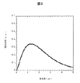
本実施例の場合は、図3に示すように、0.05nm以上4nm以下の直径を有する空孔を主として含む分布特性を有する微小空孔が存在する絶縁膜であり、比誘電率は2.3程度である。
【0079】
径分布は、理学電機(株)製X線薄膜構造解析装置(型式:ATX?G)を用いて得られるX線反射測定データと散漫散乱X線測定データを基に、球状散乱体を想定した散乱関数に基づく理論散乱強度と比較して、散乱体の径分布を算出することで求めた。
【0080】
また、上述の微小空孔を膜中に有する絶縁膜は、ヤング率12Gaの特性を有する。これら特性は、米国MTSシステムズ社製NanoindenterXPを使用したインデンテーション測定法を用い、Siウエハ上に形成した膜厚250nmの同膜について、総膜厚の1/5の表層点での硬度によって上述の膜硬度を求めた。
【0081】
また、ヤング率も総膜厚の1/5の表層点での値であり、溶融石英のポアソン比0.17を基に換算した。同様の手法で求めた同程度の膜厚のp?TEOS膜は、ヤング率70Gaの特性を有する。
【0082】
これから、上述の微小空孔を膜中に有する絶縁膜は、p?TEOS膜の約17%のヤング率を有する膜で、特開2000?340569号公報に記載されている低誘電率膜に比べて、機械的特性に優れた低誘電率絶縁膜が得られた。
【0083】
これにより、多層構造の下層部において、比誘電率が2.5未満で膜強度に優れた絶縁膜を用い、また、多層構造の上層部において、シリコン酸化膜より比誘電率の小さいフッ素添加シリコン酸化膜を用いることで、層間絶縁膜全体の誘電率を下げ、素子構造の機械的強度の低下を抑えながら高性能の半導体装置が得られた。
【0084】
(第14の実施例)
第13の実施例と同様の手法を用いて、本実施例では絶縁層102、104、106、108、110、112について、CVD法を用いてシリコン炭化膜を成膜した。
【0085】
次に、最上層にシリコン窒化膜114を形成し、6層のCu配線115を備える多層配線半導体素子を作製した。
【0086】
これにより、エッチングストッパー膜や拡散バリア膜として、シリコン窒化膜より比誘電率の低いシリコン炭化膜を用い、また、微小空孔を膜中に有する絶縁膜を用いて、空孔径を規定することで機械的特性に優れた低誘電率絶縁膜が得られる。
【0087】
そして、さらには多層積層構造の下層部において、第2の絶縁層として比誘電率が2.5未満で膜強度に優れた絶縁膜を用い、また、多層構造の上層部において、第2の絶縁層にシリコン酸化膜より比誘電率の小さいフッ素添加シリコン酸化膜を用いることで、層間絶縁膜全体の誘電率を下げ、素子構造の機械的強度の低下を抑えながら高性能の半導体装置が得られた。
【0088】
(第15の実施例)
第13の実施例と同様の手法を用いて、本実施例では、絶縁層103、105、107、109について、シルセスキオキサン水素化合物を主成分とするメチルイソブチルケトン溶液を、塗布方法を用いて基板の上に形成した後、窒素雰囲気中で、ホットプレートを用いて100℃で10分間、次いで150℃で10分間、230℃で10分間の加熱を行った。
【0089】
そしてさらに、窒素雰囲気中炉体を用いて350℃で30分間加熱することによって、Si−O−Si結合をラダー構造的に形成し、最終的にはSiOを主成分として、空孔形成を制御した微小空孔を膜中に有する絶縁膜を形成し、6層のCu配線115を備える多層配線半導体素子を作製した。開口形成は、SiOをエッチングするガスを用いて、ドライエッチング方式で行った。
【0090】
本実施例の場合は、図4に示すように、0.05nm以上1nm以下の直径を有する空孔を主として含む分布特性を有する微小空孔が存在する絶縁膜であり、比誘電率は2.7程度である。
【0091】
径分布は、X線薄膜構造解析装置を用いて得られるX線反射測定データと散漫散乱X線測定データを基に、球状散乱体を想定した散乱関数に基づく理論散乱強度と比較して、散乱体の径分布を算出することで求めた。
【0092】
また、上述の微小空孔を膜中に有する絶縁膜は、ヤング率11Gaの特性を有する。これら特性は、NanoindenterXPを使用したインデンテーション測定法を用い、Siウエハ上に形成した膜厚250nmの同膜について、総膜厚の1/5の表層点での硬度によって上述の膜硬度を求めた。
【0093】
また、ヤング率も総膜厚の1/5の表層点での値であり、溶融石英のポアソン比0.17を基に換算した。同様の手法で求めた同程度の膜厚のp?TEOS膜は、ヤング率70Gaの特性を有する。
【0094】
これから、上述の微小空孔を膜中に有する絶縁膜は、p?TEOS膜の約16%のヤング率を有する膜で、特開2000?340569号公報に記載されている低誘電率膜に比べて、機械的特性に優れた低誘電率絶縁膜が得られた。
【0095】
以上により、多層積層構造の下層部において、第2の絶縁層として比誘電率が3.0未満で膜強度に優れた絶縁膜を用い、また、多層積層構造の上層部において、第2の絶縁層にシリコン酸化膜より比誘電率の小さいフッ素添加シリコン酸化膜を用いることで、層間絶縁膜全体の誘電率を下げ、素子構造の機械的強度の低下を抑えながら高性能の半導体装置が得られた。
【0096】
(第16の実施例)
第15の実施例と同様の手法を用いて、本実施例では絶縁層102、104、106、108、110、112について、CVD法を用いてシリコン炭化膜を成膜した。次に、最上層にシリコン窒化膜114を形成し、6層のCu配線115を備える多層配線半導体素子を作製した。
【0097】
これにより、エッチングストッパー膜や拡散バリア膜として、シリコン窒化膜より比誘電率の低いシリコン炭化膜を用い、また、微小空孔を膜中に有する絶縁膜を用いて、空孔径を規定することで機械的特性に優れた低誘電率絶縁膜が得られた。そして、多層積層構造の下層部において、第2の絶縁層として比誘電率が3.0未満で膜強度に優れた絶縁膜を用い、また、多層構造の上層部において、第2の絶縁層にシリコン酸化膜より比誘電率の小さいフッ素添加シリコン酸化膜を用いることで、層間絶縁膜全体の誘電率を下げ、素子構造の機械的強度の低下を抑えながら高性能の半導体装置が得られた。
【0098】
(第17の実施例)
第17の実施例は、Cu配線デュアルダマシン構造の形成に適用した例であって、図5(a)〜(d)の工程図を用いて説明する。
【0099】
一般的に良く知られた方法を用いてMOSトランジスタ等の構成素子(図示省略)を形成した半導体基板501上に、第1配線層の第1絶縁層となるシリコン炭化窒化膜502を40nm厚でCVD法を用いて形成した。この第1絶縁層は、配線パターンを形成する開口時にエッチングストッパー膜となる。
【0100】
次に、シルセスキオキサン水素化合物を主成分とするメチルイソブチルケトン溶液を、塗布方法を用いて基板の上に形成した後、窒素雰囲気中で、ホットプレートを用いて100℃で10分間、次いで150℃で10分間、230℃で10分間の加熱を行った。そしてさらに、窒素雰囲気中炉体を用いて350℃で30分間加熱することによって、Si−O−Si結合をラダー構造的に形成し、最終的にはSiOを主成分として、図3に示すように、0.05nm以上4nm以下の直径を有する空孔を主として含む分布特性を有する微小空孔が存在する比誘電率2.3程度の絶縁膜を形成し、第1配線層の第2絶縁層503とした。
【0101】
次に、第1配線層の第3絶縁層となるシリコン炭化窒化膜504を40nm厚でCVD法を用いて形成した。この膜は、第2配線層の第1絶縁層として配線パターンを形成する開口時にエッチングストッパー膜やCu拡散バリア膜としての役目も果たす。
【0102】
次に、シリコン炭化窒化膜504に開口517を形成した。開口は、フォトレジストを用いて、周知の技術でレジストパターンを形成し、シリコン炭化窒化膜を除去できるエッチングガスを用いて、レジストをマスクにしてドライエッチング方式を用いて形成した(図5(a))。このとき、開口は第1配線層の配線寸法となっている。
【0103】
次に、第1配線層の第2絶縁層503形成と同様の方法を用いて、第2配線層の第2絶縁層となる、図3に示すように0.05nm以上4nm以下の直径を有する空孔を主として含む分布特性を有する微小空孔が存在する比誘電率2.3の絶縁層505を400nm厚で、第3絶縁層となるシリコン炭化窒化膜506を40nm厚で形成した。
【0104】
次に、シリコン炭化窒化膜に開口518を形成した(図5(b))。開口は、フォトレジストを用いて、周知の技術でレジストパターンを形成し、シリコン炭化窒化膜を除去できるエッチングガスを用いて、レジストをマスクにしてドライエッチング方式を用いて形成した。
【0105】
次に、シリコン炭化窒化膜をマスクにして微小空孔を有するSiO膜を除去できるガスを用いてドライエッチング方式で、絶縁層505に開口を形成し、その下部でシリコン炭化窒化膜504の開口517が露出する。
【0106】
引き続き、シリコン炭化窒化膜504の開口517をマスクに、絶縁層503に開口を形成し、その下部でシリコン炭化窒化膜502を露出させた。続いて、シリコン炭化窒化膜を除去できるエッチングガスに切替え、絶縁層503の開口をマスクに、シリコン炭化窒化膜502をドライエッチング除去し、半導体基板501に貫通する開口を形成した。このとき、シリコン炭化窒化膜504もエッチングされて、最上層のシリコン炭化窒化膜の開口518と同じ寸法に広がる。これにより、半導体基板501に貫通する配線溝519を形成した(図5(c))。
【0107】
次に、配線溝119内面にバリアメタル膜120を形成した後、良く知られたメッキ法を用いてCu121の充填を行った。バリアメタルは、本実施例ではTiNを用いた。
【0108】
そして、化学機械研磨法を用いて最上層であるシリコン炭化窒化膜上に存在する不要なCu膜を除去し、表面を洗浄することで、接続用プラグと配線を同時に形成した。この研磨工程で、最上層に当たるシリコン炭化窒化膜506は研磨除去せずに残した。これにより、Cu配線(520及び521を含む)を形成したデュアルダマシン構造を作製した(図5(d))。
【0109】
上記のように、層間絶縁膜層の主要な構成層である第2の絶縁層503に比誘電率の低い膜を用いることで、層間絶縁膜全体の誘電率を下げた高性能の半導体装置が得られる。
【0110】
本実施例の構成では配線層を2層積層した構造であるが、配線層を2回以上繰り返して積み上げることで多層配線構造を有する半導体装置が得られる。
【0111】
(第18の実施例)
第17の実施例と同様にして、本実施例では第2の絶縁層503について図4に示すように、0.05nm以上1nm以下の直径を有する空孔を主として含む分布特性を有する微小空孔が存在する比誘電率2.7程度のSiO絶縁膜を形成し、Cu配線を形成したデュアルダマシン構造を作製した。
【0112】
これにより、層間絶縁膜層の主要な構成層である503に関して、比誘電率の低い膜を用いることで、層間絶縁膜全体の誘電率を下げた高性能の半導体装置が得られる。さらにまた、配線層を2回以上繰り返して積み上げることで多層配線構造を有する高性能の半導体装置が容易に得られる。
【0113】
(第19の実施例)
図6は第19の実施例である半導体ロジック素子の断面図である。半導体基板601上に既知のSTI(Shallow Trench Isolation)を用いて素子分離膜領域602を形成し、この素子分離膜領域602内部にMOSトランジスタ603を形成する(トランジスタ部のハッチングは図を見易くするために省略した)。そして、既知のCVD法を用いて50nm程度のシリコン酸化膜604と500nm程度のBPSG(ボロン・リン・シリケイトガラス)膜605とを、MOSトランジスタ603を含み、半導体基板601の表面に順次形成した後、例えば800〜900℃の窒素雰囲気でリフローアニールする。
【0114】
次に、シリカ砥粒を用いた化学機械研磨法を用いてBPSG膜605の表面を平坦化研磨した後、コンタクトホールを形成し、このコンタクトホール内に、CVD法によりタングステンの埋め込みを行い、導電プラグ606を形成する。この時、BPSG膜605の表面上に存在する不要なタングステンは既知のエッチバック法により除去されている。
【0115】
次に、第17の実施例と同様にして、第1配線層の第1絶縁層となるシリコン炭化窒化膜607を40nm厚でCVD法を用いて形成した。この第1絶縁層は、配線パターンを形成する開口時にエッチングストッパー膜となる。
【0116】
次に、シルセスキオキサン水素化合物を主成分とするメチルイソブチルケトン溶液を、塗布方法を用いて基板の上に形成した後、窒素雰囲気中で、ホットプレートを用いて100℃で10分間、次いで150℃で10分間、230℃で10分間の加熱を行った。そしてさらに、窒素雰囲気中炉体を用いて350℃で30分間加熱することによって、Si−O−Si結合をラダー構造的に形成し、最終的にはSiOを主成分として、図3に示すように、0.05nm以上4nm以下の直径を有する空孔を主として含む分布特性を有する微小空孔が存在する比誘電率2.3程度の絶縁膜を形成し、第1配線層の第2絶縁層608とした。
【0117】
次に、第1配線層の第3絶縁層となるシリコン炭化窒化膜609を40nm厚でCVD法を用いて形成した。この膜は、第2配線層の第1絶縁層として配線パターンを形成する開口時にエッチングストッパー膜やCu拡散バリア膜としての役目も果たす。
【0118】
次に、シリコン炭化窒化膜609に開口を形成した。開口は、フォトレジストを用いて、周知の技術でレジストパターンを形成し、シリコン炭化窒化膜を除去できるエッチングガスを用いて、レジストをマスクにしてドライエッチング方式を用いて形成した。このとき、開口は第1配線層の配線寸法となっている。
【0119】
次に、第1配線層の第2絶縁層608形成と同様の方法を用いて、第2配線層の第2絶縁層610を400nm厚で、第3絶縁層となるシリコン炭化窒化膜611を40nm厚で形成した。
【0120】
次に、シリコン炭化窒化膜に開口を形成した。そして、このシリコン炭化窒化膜をマスクにして微小空孔を有するSiO膜を除去できるガスを用いてドライエッチング方式で、絶縁層610に開口を形成し、その下部でシリコン炭化窒化膜609が露出する。
【0121】
引き続き、シリコン炭化窒化膜609の開口をマスクに、絶縁層608に開口を形成し、その下部でシリコン炭化窒化膜607を露出させた。そして、シリコン炭化膜を除去できるエッチングガスに切替え、絶縁層608の開口をマスクに、シリコン炭化窒化膜607をドライエッチング除去し、導電プラグ606に貫通する開口を形成した。
【0122】
このとき、シリコン炭化窒化膜609もエッチングされて、最上層のシリコン炭化膜の開口と同じ寸法に広がる。これにより、導電プラグ606に貫通する配線溝を形成した。
【0123】
次に、配線溝内面にバリアメタル膜を形成した後、良く知られたメッキ法を用いてCuの充填を行った。バリアメタルは、本実施例ではTiNを用いた。そして、化学機械研磨法を用いて最上層であるシリコン炭化窒化膜上に存在する不要なCu膜を除去し、表面を洗浄することで、接続用プラグと配線を同時に形成した。この研磨工程で、最上層に当たるシリコン炭化膜611は研磨除去せずに残した。これにより、Cu配線を形成したデュアルダマシン構造を作製した。
【0124】
以上の工程を繰り返して4層配線構造体を形成した。
続いて、同様の工程を繰り返してさらに2層の配線構造を積み上げた。このとき、絶縁層617、619,621はシリコン炭化窒化膜を用いて40nm厚で形成した。また、絶縁層618、620は、フッ素添加シリコン酸化膜を用いて600nm厚で形成した。次に、最上層にシリコン窒化膜622を形成し、6層のCu配線623を備える多層配線半導体素子を作製した。
【0125】
これにより、エッチングストッパー膜や拡散バリア膜として、シリコン窒化膜より比誘電率の低いシリコン炭化膜を用い、多層積層構造の下層部において、第2の絶縁層として比誘電率が2.5未満で膜強度に優れた絶縁膜を用い、また、その上層部において、第2の絶縁層にシリコン酸化膜より比誘電率の小さいフッ素添加シリコン酸化膜を用いることで、層間絶縁膜全体の誘電率を下げた高性能の半導体装置が得られた。
【0126】
(第20の実施例)
図7に、第20の実施例である樹脂封止された半導体ロジック装置の断面図を示す。第19の実施例で得られ、ボンディングパッド部を除いてポリイミド表面保護膜702を形成した状態の半導体ロジック装置701に、別途設けられているダイボンディング工程におけるリードフレームに固定する。その後、半導体ロジック装置701に設けられたボンディングパッド部とリードフレームの外部端子705の間を、ワイヤーボンダーを用いて金線704を配線した。
【0127】
次に、日立化成工業(株)製のシリカ含有ビフェニル系エポキシ樹脂を用いて、半導体ロジック装置701、外部端子705等を包み込むように樹脂封止部703を形成した。封止条件は、成型温度180℃、成型圧力70kg/cm2であるが、これに限定されるものではない。最後に、外部端子706を所定の形に折り曲げることにより、樹脂封止型半導体ロジック装置の完成品が得られる。
【0128】
樹脂封止された半導体ロジック装置の層間絶縁膜の一部には、比誘電率の小さいが機械的強度の低下を十分に抑制した絶縁膜が使用されているので、ワイヤボンディングプロセスや樹脂封止プロセスにおいて、半導体ロジック素子にかかる応力に対して、素子内部にクラックが発生することなく、樹脂封止品が得られる。
【0129】
また、半導体ロジック素子の特性として第19の実施例で説明した同様の効果を奏することは言うまでもなく、さらに樹脂封止されているので外部環境に対して安定な特性を発揮することが可能である。
【0130】
(第21の実施例)
図8は、第21の実施例を説明するための断面図であって、第19の実施例で説明した半導体ロジック素子をウエハレベルチップサイズパッケージ構造の製品の製造に用いた場合である。
【0131】
半導体ロジック素子801の最上層シリコン窒化膜802上にボンディングパッド部803を露出させる形状でポリイミド絶縁膜804を形成する。次に、再配列配線805を形成する。本実施例では、再配列配線は、TiN、Cu、Niをスパッタ法で成膜した3層からなり、成膜後に周知のフォトリソ技術で配線パターンを形成したものである。
【0132】
さらにその上にポリイミド絶縁膜806を形成した。このポリイミド絶縁膜層806を貫いて再配列配線805の一部の領域で電気的な接続を行うためのアンダーバンプメタル層807を設けた。アンダーバンプメタル層はCr、Ni、Auの3層形成した。このアンダーバンプメタル層807の上にハンダバンプ808が形成されている。
【0133】
高速駆動の可能な半導体ロジック素子そのものは第19の実施例で述べた方法によってウエハ上に形成することができるため、本実施例によってウエハの状態でハンダバンプを有する半導体ロジックパッケージ装置が実現する。
【0134】
誘電率の低い層間絶縁膜層を適用することで、従来製品に比べて高性能の半導体ロジック素子はすでに得られている。しかしながら、パッケージ半導体製品をプリント基板などに実装搭載する場合に、本実施例のようなパッケージ構造を適用することで、素子とプリント基板間の信号伝播を高速に行えることが可能となり、半導体ロジック素子の性能をさらに引き出せることが可能となる。
【0135】
(第22の実施例)
図9に、第22の実施例を説明するための素子端部の断面図(図9(a))及びウエハ平面概念図(図9(b))を示す。
【0136】
シリコン基板901にはMOSトランジスタ等の半導体素子906やこれらの素子を含む半導体回路部が形成されており、この基板901の上に上記で説明した配線層が形成されている。そして、この半導体素子906やこれらの素子を含む半導体回路部を囲むように、配線層を構成する導体からなる材料を用いてガードリング層905が配置されている。このガードリング層905によって、半導体素子906やこれらの素子を含む半導体回路部を外部からの水分の浸入を防ぐことができる。このガードリング層905は、導体配線を形成する工程において形成される。
【0137】
これにより、特に低誘電率特性を示す層間絶縁膜として空孔を有する絶縁膜を適用した場合、孔内部への水分の透過や吸着の問題点を解決し、半導体素子自体の耐湿信頼性を向上させた半導体装置を提供できる。
【0138】
以上、実施例を用いて詳細に説明したが、本発明並びに実施例を達成するための諸条件等はこれらの実施例に何ら限定されるものではない。
【0139】
【発明の効果】
以上説明したように、配線抵抗を下げた銅配線を層間絶縁膜層に埋め込むダマシン構造を適用した多層積層配線を有する半導体素子において、エッチングストッパー膜や拡散バリア膜としてシリコン窒化膜より小さい比誘電率の膜を用い、そして多層積層構造の下層部と上層部における絶縁膜を異なるようにすることで、素子全体の機械的強度を高め、かつ、層間絶縁膜全体の誘電率を下げた高性能の半導体装置が得ることができる。
【図面の簡単な説明】
【図1】第1の実施例で作製した積層構造の半導体装置の断面図である。
【図2】第1の実施例で作製した半導体装置を説明するための工程図である。
【図3】絶縁膜中に存在する空孔の径分布を説明するための図である。
【図4】絶縁膜中に存在する空孔の径分布を説明するための図である。
【図5】第17の実施例で作製した積層構造の半導体装置を説明するための工程図である。
【図6】第19の実施例で作製した半導体ロジック装置を説明するための断面図である。
【図7】第20の実施例で作製した樹脂封止型半導体装置を説明するための断面図である。
【図8】第21の実施例で作製したウエハレベルチップサイズパッケージ構造半導体装置を説明するための断面図である。
【図9】第22の実施例で作製したガードリング構造を有する半導体装置を説明するための断面図及び平面図である。
【符号の説明】
101…半導体基板、102…1層配線層の第1絶縁膜、103…1層配線層の第2絶縁膜、104…1層配線層の第3絶縁膜/2層配線層の第1絶縁膜、105…2層配線層の第2絶縁膜、106…2層配線層の第3絶縁膜/3層配線層の第1絶縁膜、107…3層配線層の第2絶縁膜、108…3層配線層の第3絶縁膜/4層配線層の第1絶縁膜、109…4層配線層の第2絶縁膜、110…4層配線層の第3絶縁膜/5層配線層の第1絶縁膜、111…5層配線層の第2絶縁膜、112…5層配線層の第3絶縁膜/6層配線層の第1絶縁膜、113…6層配線層の第2絶縁膜、114…最表面パッシベーション膜(シリコン窒化膜)、115…導体配線層、117…開口、118…開口、119…配線溝、120…バリアメタル膜、121…導体層、501…半導体基板、502…1層配線層の第1絶縁膜、503…1層配線層の第2絶縁膜、504…1層配線層の第3絶縁膜/2層配線層の第1絶縁膜、505…2層配線層の第2絶縁膜、506…2層配線層の第3絶縁膜、517…開口、518…開口、519…配線溝、520…バリアメタル膜、521…導体層、601…半導体基板、602…素子分離膜領域、603…MOSトランジスタ、604…シリコン酸化膜、605…BPSG(ボロン・リン・シリケイトガラス)膜、606…導電プラグ、607…1層配線層の第1絶縁膜、608…1層配線層の第2絶縁膜、609…1層配線層の第3絶縁膜/2層配線層の第1絶縁膜、610…2層配線層の第2絶縁膜、611…2層配線層の第3絶縁膜、612…3層配線層の第1絶縁膜、613…3層配線層の第2絶縁膜、614…3層配線層の第3絶縁膜/4層配線層の第1絶縁膜、615…4層配線層の第2絶縁膜、616…4層配線層の第3絶縁膜、617…5層配線層の第1絶縁膜、618…5層配線層の第2絶縁膜、619…5層配線層の第3絶縁膜/6層配線層の第1絶縁膜、620…6層配線層の第2絶縁膜、621…6層配線層の第3絶縁膜、622…最表面パッシベーション膜(シリコン窒化膜)、623…導体配線層、701…半導体ロジック装置、702…チップコート膜、703…樹脂封止部(エポキシ樹脂)、704…金線、705…リードフレーム、706…外部端子、801…半導体基板、802…SiNパッシベーション膜、803…ボンディングパッド、804…絶縁膜層、805…再配列配線、806…絶縁膜層、807…アンダーバンプメタル層、808…はんだ、901…半導体基板、902…パッシベーション膜(シリコン窒化膜)、903…スクライブライン、904…ガードリング層、905…素子装置周辺ガードリング層、906…半導体素子。[0001]
TECHNICAL FIELD OF THE INVENTION
The present invention relates to a semiconductor device in which a signal wiring delay is reduced by using an insulating film having low dielectric constant characteristics as an interlayer insulating film, thereby improving element performance.
[0002]
[Prior art]
With the increase in the degree of integration of semiconductor elements and the reduction in chip size, finer wiring, narrower pitches, and multilayering are being promoted. Along with this, a delay time when a signal propagates through a wiring, that is, a wiring delay tends to increase, which is a major problem when using an electronic device using a semiconductor element.
Generally, the speed of a signal propagating through a wiring is determined by the product (RC) of the wiring resistance (R) and the capacitance between wirings (C). Therefore, reducing the wiring resistance or reducing the capacitance between wirings, that is, an interlayer insulating film It is necessary to lower the dielectric constant in order to reduce wiring delay.
[0003]
In order to reduce the wiring resistance, in the case of high-performance semiconductor devices, the wiring material is being changed from aluminum to copper, and the process application of the damascene structure, in which copper wiring is buried in the interlayer insulating film layer, has been actively performed. Have been
[0004]
In order to reduce the dielectric constant of an interlayer insulating film, a silicon oxide film (SiO 2) conventionally formed by a CVD (Chemical Vapor Deposition) method is used for an interlayer insulating film of a semiconductor device. 2 : A relative dielectric constant of about 4.0) or an inorganic material such as a silicon nitride film (Si-N: a relative dielectric constant of about 7.0). As a low dielectric constant material that can follow the conventional process, recently, a fluorine-added silicon oxide film (Si-OF: a relative dielectric constant of about 3.6) has been successively adopted.
[0005]
However, the dielectric constant of the fluorine-doped silicon oxide film is relatively high, and when this is used as an interlayer insulating film, the effect of reducing the interlayer capacitance is not sufficient. A material having a modulus is needed.
[0006]
Various materials have been proposed as interlayer insulating film materials having a relative dielectric constant of less than 3.5, and when roughly classified, a so-called spin-on-glass material, which forms a film by heating after being applied to a substrate, or a similar material. An organic material for forming a film and a technique for forming a film using a CVD method are also being studied.
[0007]
Examples of the spin-on-glass material include a material containing a hydrogen silsesquioxane (Hydrogen Silsesquioxane) compound or a methyl silsesquioxane methyl (Methyl Silsesquioxane) compound. A material containing a silsesquioxane hydrogen compound or a silsesquioxane methyl compound as a main component is preferable. In this specification, the main component refers to a component having the highest blending ratio (molar ratio).
[0008]
The coating solution containing a silsesquioxane hydrogen compound as a main component has a general formula (HSiO 3/2 ) n Is dissolved in a solvent such as methyl isobutyl ketone. This solution is applied to a substrate, heated intermediately at a temperature of about 100 to 250 ° C., and then heated at a temperature of 350 to 450 ° C. in an inert atmosphere such as a nitrogen atmosphere, thereby forming Si—O—Si. The bond is formed in a ladder structure, and finally an insulating film containing SiO as a main component is formed.
[0009]
A coating solution containing a silsesquioxane methyl compound as a main component has a general formula (CH 3 SiO 3/2 ) n Is dissolved in a solvent such as methyl isobutyl ketone. This solution is applied to a substrate, heated intermediately at a temperature of about 100 to 250 ° C., and then heated at a temperature of 350 to 450 ° C. in an inert atmosphere such as a nitrogen atmosphere, thereby forming Si—O—Si. The bond is formed in a ladder structure, and finally an insulating film containing SiO as a main component is formed.
[0010]
As an organic insulating film material, polymer materials such as polyimide, polyparaxylylene, polyarylene ether, polyarylene, benzcyclobutene, and polynaphthalene, which are hydrocarbon resins, are known. These materials achieve a low dielectric constant by reducing the density of the film by containing carbon atoms and by reducing the polarizability of the molecule (monomer) itself.
[0011]
As a technique for further reducing the relative dielectric constant of an interlayer insulating film such as the above-described spin-on-glass film, organic film, or CVD film, it is known to form a porous film by forming minute holes in the film. The above materials and processes are disclosed in "International Technology Roadmap for Semiconductors" (ed. 1999), pp. 163-186, JP-A-2000-340569, and JP-A-2001-274239.
[0012]
However, in the above-described conventional technology, an interlayer insulating film having a characteristic whose relative dielectric constant is lower than 3.5 has a mechanical property such as hardness and elastic modulus of the insulating film, which is lower than that of a silicon oxide film or a silicon nitride film formed by CVD. There is a problem that the strength is essentially low.
[0013]
In such an insulating film, forming pores in the film to make the film porous to further reduce the relative dielectric constant is in the direction of further deteriorating the mechanical strength, and is not realistic. It had been.
[0014]
As a means for lowering the relative dielectric constant of the insulating film, an insulating organic polymer such as polyimide may be used. Organic polymers are advantageous because their relative dielectric constants are less than 4, but they have disadvantages in that they are physically lower in mechanical strength and higher in hygroscopicity and moisture permeability than inorganic films. In addition, when used as an interlayer insulating film, there is a problem in reliability of the device, such as a decrease in mechanical strength of the device structure and corrosion of wiring due to moisture absorption.
[Non-patent document 1]
"International Technology Roadmap for Semiconductors" (1999), pp. 163-186.
[Patent Document 1]
JP 2000-340569 A
[Patent Document 2]
JP 2001-274239 A
[0015]
[Problems to be solved by the invention]
Therefore, in particular, in a multilayer wiring semiconductor element using a damascene structure in which copper wiring with reduced wiring resistance is embedded in an interlayer insulating film layer, the dielectric constant of the entire interlayer insulating film is reduced while suppressing a decrease in mechanical strength of the element structure. The method was examined.
[0016]
Based on the technical background described above, the present invention has a laminated structure of a film having a low dielectric constant and a film having a high dielectric constant as described above, and by optimizing the combination and structure of each material, An object of the present invention is to propose a method for realizing both electrical characteristics and mechanical characteristics of an insulating film itself.
[0017]
In particular, in a semiconductor device having a laminated structure employing a damascene structure in which copper wiring with reduced wiring resistance is embedded in an interlayer insulating film layer, a signal delay propagating through the wiring is suppressed while suppressing a decrease in mechanical strength of the interlayer insulating film. A highly reliable and high-performance semiconductor device with reduced characteristics has been made possible.
[0018]
[Means for Solving the Problems]
The semiconductor device of the present invention has a structure in which a first insulating layer, a second insulating layer, a third insulating layer, and the three insulating layers are formed on a substrate on which a transistor element and a semiconductor circuit portion are formed. This is a semiconductor device formed by laminating a plurality of wiring layers each having the formed conductor wiring. At this time, the first and third insulating layers constituting each wiring layer are made of a silicon carbonitride film, a silicon carbide, or a silicon oxide. The insulating layer of Example 1 contains silicon oxide, and the second insulating layer of the wiring layer located on the upper layer part contains silicon oxide containing fluorine or silicon oxide.
[0019]
At this time, when a copper wiring is used as a conductor wiring, the first insulating film serves as an etching stopper film when the insulating film is opened to bury the copper wiring. Further, the third insulating layer becomes a diffusion barrier film for the copper wiring.
[0020]
Conventionally, a silicon nitride film has been used as an etching stopper film and a diffusion barrier film. In the present invention, a silicon carbonitride film having a lower relative dielectric constant than a silicon nitride film (Si—CN: about 4.6). Since a film made of silicon carbide (Si—C: relative dielectric constant of about 4.4) or silicon oxide is used, the relative dielectric constant of the entire wiring layer having a multilayer structure can be reduced.
[0021]
Among the wiring layers, the second insulating layer of the wiring layer located on the upper layer portion is made of a fluorine-doped silicon oxide film or a carbon-doped silicon oxide film having a relative dielectric constant smaller than that of the silicon oxide film (a relative dielectric constant of about 2.9). Thereby, the relative dielectric constant of the entire wiring layer can be reduced as compared with the case where all the second insulating layers constituting the wiring layer are made of silicon oxide.
[0022]
Further, in the semiconductor device of the present invention, the second insulating layer of the lower wiring layer is made of an insulating film material having a relative dielectric constant of less than 3.0, and the second insulating layer of the upper wiring layer is formed of an insulating film material. It was made of a fluorine-added silicon oxide film or a carbon-added silicon oxide film. That is, the constituent components of the second insulating layer are made different between the wiring layer located in the upper layer portion and the wiring layer located in the lower layer portion so that the relative dielectric constant of the latter insulating film is smaller than that of the former. did.
[0023]
Further, in the semiconductor device of the present invention, the second insulating layer of the lower wiring layer has a characteristic of a relative dielectric constant of less than 3.0, is an insulating film containing SiO, and has Or more of the micropores existing in the sample had a diameter of 0.05 nm or more and 4 nm or less. In the present invention, it is preferable that the main configuration of the micropores has a diameter of 0.05 nm or more and 4 nm or less. According to the present invention, a multi-layer laminated structure is obtained by using a SiO-containing insulating film having a relative dielectric constant of less than 3.0 as a single film by reducing the density of the film by having micropores in the film. In the entire wiring layer, the relative dielectric constant can be further reduced.
[0024]
At this time, the relative permittivity of the insulating film is reduced from the relative permittivity of the silicon oxide film by using a method in which minute holes are formed in the insulating film to lower the density and approach the relative permittivity of vacuum. In particular, by controlling the size and density of the minute holes, an insulating film having an arbitrary relative dielectric constant can be formed.
[0025]
However, as the diameter of the micropores increases, the mechanical strength of the insulating film itself as a structure decreases, or the leakage current flowing through the insulating film increases, thereby lowering the dielectric strength characteristic of the insulating film. The problem described above also newly arises, and it is necessary to pay close attention to the size of the holes contained in the insulating film.
[0026]
Therefore, in the present invention, by controlling the range of the pore diameter, a decrease in the mechanical strength and the dielectric strength of the insulating film is suppressed. At this time, when at least half of the minute holes have a diameter of 0.05 nm or more and 4 nm or less, a highly reliable semiconductor device can be provided without reducing the film strength of the insulating film.
[0027]
The insulating film having microvoids is formed of an insulating film mainly containing SiO, which is obtained by heating a film mainly containing a silsesquioxane hydrogen compound or a silsesquioxane methyl compound.
[0028]
The coating solution containing a silsesquioxane hydrogen compound as a main component has a general formula (HSiO 3/2 ) n Is dissolved in a solvent such as methyl isobutyl ketone. A coating solution containing a silsesquioxane methyl compound as a main component is represented by the general formula (CH 3 SiO 3/2 ) n Is dissolved in a solvent such as methyl isobutyl ketone.
[0029]
These solutions are applied to a substrate, intermediately heated at a temperature of about 100 to 250 ° C., and then heated at a temperature of 350 to 450 ° C. in an inert atmosphere such as a nitrogen atmosphere to obtain Si—O—Si. Are formed in a ladder structure, and finally an insulating film containing SiO as a main component is formed.
[0030]
As a method for controlling the diameter of pores present in an insulating film in an insulating film mainly containing SiO obtained by heating a film mainly containing a silsesquioxane hydrogen compound or a silsesquioxane methyl compound, For example, a solution other than a solvent such as methyl isobutyl ketone is added to a solution of a silsesquioxane compound in a silsesquioxane compound solution, and traces of the decomposition of the component are formed as pores in the film, and the decomposition behavior changes depending on the film formation temperature. By doing so, there is a method of controlling the formation of holes and making it possible to keep the hole diameter range within a selective range.
[0031]
As a method of applying the above-mentioned solution for forming an insulating film, spin coating, slit coating or a printing method may be used. Since the insulating film is formed by heating this film, even if fine wiring is formed at high density, the step coverage is better than that of the insulating film formed by the CVD method. This is advantageous in that surface steps can be eliminated.
[0032]
In addition, in order to increase the diameter of a Si wafer, when an insulating film is formed using a CVD method, a large-sized film forming apparatus is required, and the equipment cost has a large effect on the element cost. On the other hand, in the present invention, since the insulating film is formed by the coating / heating method, the equipment cost can be significantly reduced, and a great effect of suppressing the investment cost of the production line and further the element cost is expected. it can.
[0033]
When an insulating film is formed by a CVD method, an alkylsilane compound or an alkoxysilane compound is used as a main component as a source gas, and finally SiO is used as a main component by an ECR (Electron Cyclotron Resonance) plasma CVD method or the like. An insulating film is formed.
[0034]
Also in this case, as a technique for controlling the diameter of the pores present in the insulating film, for example, a component having a high thermal decomposition temperature is contained as a source gas, and the film is heated at 350 ° C. to 450 ° C. during film formation to form a film. There is a method in which traces of the decomposition of this component are formed as pores.
[0035]
In such a method, it is possible to change the decomposition behavior depending on the film formation temperature by selecting various components having a high thermal decomposition temperature, and thereby selectively control the pore formation, thereby selectively controlling the pore diameter range. Within the optimal range.
[0036]
Further, in the semiconductor device of the present invention, in order to prevent moisture absorption and moisture permeation from the periphery of the semiconductor device, a partition layer (referred to as a guard ring in the present invention) made of a material forming a conductor wiring so as to surround the periphery of the element device. Is provided around the element device. Thus, according to the present invention, the moisture permeating the inside of the interlayer insulating film from around the element or from the interface between the substrate and the interlayer insulating film can be shielded, and the humidity resistance reliability of the element itself can be improved.
[0037]
BEST MODE FOR CARRYING OUT THE INVENTION
Hereinafter, embodiments of the present invention will be described with reference to the drawings.
[0038]
(First embodiment)
In the first embodiment, as shown in FIG. 1, a six-layer wiring semiconductor element having a Cu wiring dual damascene structure having six wiring layers 100 was manufactured.
[0039]
A
[0040]
Next, a
[0041]
Next, a
[0042]
Next, an
[0043]
Next, using a method similar to that for forming the first wiring layer 100a, a
[0044]
Next, an
[0045]
Next, an opening is formed in the
[0046]
Subsequently, an opening was formed in the
[0047]
Subsequently, the etching gas was changed to an etching gas capable of removing the silicon carbonitride film, and the
[0048]
Next, after a
[0049]
Then, an unnecessary Cu film existing on the silicon carbonitride film as the uppermost layer was removed, and the surface was washed, thereby simultaneously forming a connection plug and a wiring. For the removal of the Cu film, it is convenient to use a chemical mechanical polishing method using alumina or silica as abrasive grains and a polishing agent comprising an additive such as a Cu complexing agent and a surfactant. is there.
[0050]
In this polishing step, the
[0051]
Subsequently, the same process was performed twice to form the third wiring layer 100c to the sixth wiring layer 100f, thereby obtaining a six-layer Cu wiring structure. At this time, the insulating
[0052]
Next, a
[0053]
As a result, a silicon carbonitride film having a lower dielectric constant than a silicon nitride film is used as an etching stopper film and a diffusion barrier film, and a fluorine-doped silicon oxide film having a lower dielectric constant than a silicon oxide film is used in an upper layer of the multilayer structure. By using the film, a high-performance semiconductor device in which the dielectric constant of the entire interlayer insulating film was lowered was obtained.
[0054]
(Second embodiment)
In the present embodiment, a fluorine-added silicon oxide film was formed also on the insulating layers 107 and 109 by using the CVD method using the same method as in the first embodiment. Next, a
[0055]
As a result, a silicon carbonitride film having a lower dielectric constant than the silicon nitride film is used as the etching stopper film and the diffusion barrier film, and a dielectric constant higher than that of the silicon oxide film in the upper part of the multilayer structure. By using a small fluorine-added silicon oxide film, a high-performance semiconductor device in which the dielectric constant of the entire interlayer insulating film was lowered was obtained.
[0056]
(Third embodiment)
In this example, a silicon carbide film was formed on the insulating
[0057]
As a result, a high-performance semiconductor device in which the dielectric constant of the entire interlayer insulating film is reduced by using a silicon carbide film having a lower dielectric constant than the silicon nitride film as the etching stopper film and the diffusion barrier film is obtained.
[0058]
(Fourth embodiment)
In this example, a silicon carbide film was formed on the insulating
[0059]
As a result, a high-performance semiconductor device in which the dielectric constant of the entire interlayer insulating film is reduced by using a silicon carbide film having a lower dielectric constant than the silicon nitride film as the etching stopper film and the diffusion barrier film is obtained.
[0060]
(Fifth embodiment)
In the present embodiment, using a method similar to that of the first embodiment, a carbon-doped silicon oxide film is formed on the insulating
[0061]
Thus, a high-performance semiconductor device in which the dielectric constant of the entire interlayer insulating film is reduced by using a carbon-doped silicon oxide film having a relative dielectric constant smaller than that of the silicon oxide film in the upper layer of the multilayer structure is obtained.
[0062]
(Sixth embodiment)
In the present embodiment, a carbon-added silicon oxide film is formed on the insulating
[0063]
Further, by using a carbon-doped silicon oxide film having a relative dielectric constant smaller than that of the silicon oxide film in an upper layer portion of 1 / or more of the multilayer structure, a high-performance semiconductor device in which the dielectric constant of the entire interlayer insulating film is reduced can be obtained. Was done.
[0064]
(Seventh embodiment)
In the present embodiment, a silicon carbide film was formed on the insulating
[0065]
As a result, a high-performance semiconductor device in which the dielectric constant of the entire interlayer insulating film is reduced by using a silicon carbide film having a lower dielectric constant than the silicon nitride film as the etching stopper film and the diffusion barrier film is obtained.
[0066]
(Eighth embodiment)
In this example, a silicon carbide film was formed on the insulating
[0067]
As a result, a high-performance semiconductor device in which the dielectric constant of the entire interlayer insulating film is reduced by using a silicon carbide film having a lower dielectric constant than the silicon nitride film as the etching stopper film and the diffusion barrier film is obtained.
[0068]
(Ninth embodiment)
In the present embodiment, a carbon-added silicon oxide film is formed on the insulating
[0069]
As a result, a carbon-doped silicon oxide film having a low relative dielectric constant is used as an insulating film in a lower layer portion of the multilayer structure, and a fluorine-doped silicon oxide film having a lower dielectric constant than the silicon oxide film is formed in an upper layer portion of the multilayer structure. By using the same, a high-performance semiconductor device in which the dielectric constant of the entire interlayer insulating film is reduced was obtained.
[0070]
(Tenth embodiment)
In the present embodiment, using the same method as that of the second embodiment, a carbon-doped silicon oxide film is formed on the insulating
[0071]
Accordingly, a carbon-doped silicon oxide film having a low relative dielectric constant is used as an insulating film in a lower layer portion of the multilayer structure, and fluorine having a lower relative dielectric constant than the silicon oxide film is used in an upper layer portion of the multilayer structure of 以上 or more. By using the added silicon oxide film, a high-performance semiconductor device in which the dielectric constant of the entire interlayer insulating film was lowered was obtained.
[0072]
(Eleventh embodiment)
In the present embodiment, a carbon-added silicon oxide film is formed on the insulating
[0073]
As a result, a carbon-doped silicon oxide film having a low relative dielectric constant is used as an insulating film in a lower layer portion of the multilayer structure, and a fluorine-doped silicon oxide film having a lower dielectric constant than the silicon oxide film is formed in an upper layer portion of the multilayer structure. By using a silicon carbide film having a lower dielectric constant than a silicon nitride film as an etching stopper film and a diffusion barrier film, a high-performance semiconductor device having a reduced dielectric constant of the entire interlayer insulating film was obtained.
[0074]
(Twelfth embodiment)
In the present embodiment, using the same method as in the fourth embodiment, a carbon-added silicon oxide film is formed on the insulating
[0075]
Accordingly, a carbon-doped silicon oxide film having a low relative dielectric constant is used as an insulating film in a lower layer portion of the multilayer structure, and fluorine having a lower relative dielectric constant than the silicon oxide film is used in an upper layer portion of the multilayer structure of 以上 or more. By using a silicon oxide film with an added silicon oxide film and a silicon carbide film with a lower dielectric constant than a silicon nitride film as an etching stopper film and a diffusion barrier film, a high-performance semiconductor device with a reduced dielectric constant of the entire interlayer insulating film is obtained. Was done.
[0076]
(Thirteenth embodiment)
In this embodiment, using a method similar to that of the first embodiment, a coating method of a methyl isobutyl ketone solution containing a silsesquioxane hydrogen compound as a main component is applied to the insulating
[0077]
Further, by heating at 350 ° C. for 30 minutes using a furnace in a nitrogen atmosphere, Si—O—Si bonds are formed in a ladder structure, and finally, the formation of vacancies is controlled using SiO as a main component. An insulating film having micropores formed in the film was formed, and a multilayer wiring semiconductor element having six layers of
[0078]
In the case of the present embodiment, as shown in FIG. 3, the insulating film has fine pores having distribution characteristics mainly including pores having a diameter of 0.05 nm or more and 4 nm or less, and has a relative dielectric constant of 2. It is about 3.
[0079]
The diameter distribution was assumed to be a spherical scatterer based on X-ray reflection measurement data and diffuse scattering X-ray measurement data obtained using an X-ray thin film structure analyzer (model: ATX? G) manufactured by Rigaku Corporation. It was obtained by calculating the diameter distribution of the scatterer in comparison with the theoretical scattering intensity based on the scattering function.
[0080]
Further, the insulating film having the above-described minute holes in the film has a characteristic of a Young's modulus of 12 Ga. These characteristics were determined by the indentation measurement method using Nanoindenter XP manufactured by U.S. MTS Systems Co., Ltd., and the above-mentioned hardness was measured at a surface point of 1/5 of the total film thickness of the same film having a film thickness of 250 nm formed on a Si wafer. The film hardness was determined.
[0081]
The Young's modulus is also a value at a surface point of 1/5 of the total film thickness, and was converted based on the Poisson's ratio of fused quartz of 0.17. A similar film thickness p? The TEOS film has a characteristic of a Young's modulus of 70 Ga.
[0082]
From now on, the insulating film having the micropores in the film is p? A TEOS film having a Young's modulus of about 17% and a low dielectric constant insulating film having more excellent mechanical properties than the low dielectric constant film described in JP-A-2000-340569 was obtained.
[0083]
Thus, in the lower layer of the multilayer structure, an insulating film having a relative dielectric constant of less than 2.5 and excellent in film strength is used, and in the upper layer of the multilayer structure, fluorine-doped silicon having a lower dielectric constant than the silicon oxide film is used. By using the oxide film, a high-performance semiconductor device was obtained while lowering the dielectric constant of the entire interlayer insulating film and suppressing a decrease in mechanical strength of the element structure.
[0084]
(14th embodiment)
In this example, a silicon carbide film was formed on the insulating
[0085]
Next, a
[0086]
As a result, a silicon carbide film having a lower dielectric constant than a silicon nitride film is used as an etching stopper film or a diffusion barrier film, and an insulating film having fine pores in the film is used to define the hole diameter. A low dielectric constant insulating film having excellent mechanical properties can be obtained.
[0087]
Further, in the lower part of the multilayer structure, an insulating film having a relative dielectric constant of less than 2.5 and excellent in film strength is used as a second insulating layer. By using a fluorine-doped silicon oxide film having a relative dielectric constant smaller than that of the silicon oxide film for the layer, a high-performance semiconductor device can be obtained while lowering the dielectric constant of the entire interlayer insulating film and suppressing a decrease in mechanical strength of the element structure. Was.
[0088]
(Fifteenth embodiment)
In this embodiment, using a method similar to that of the thirteenth embodiment, a methyl isobutyl ketone solution containing a silsesquioxane hydrogen compound as a main component is applied to the insulating
[0089]
Further, by heating at 350 ° C. for 30 minutes using a furnace in a nitrogen atmosphere, Si—O—Si bonds are formed in a ladder structure, and finally, the formation of vacancies is controlled using SiO as a main component. An insulating film having micropores formed in the film was formed, and a multilayer wiring semiconductor element having six layers of
[0090]
In the case of this embodiment, as shown in FIG. 4, the insulating film has microvoids having distribution characteristics mainly including pores having a diameter of 0.05 nm or more and 1 nm or less, and has a relative dielectric constant of 2. It is about 7.
[0091]
The diameter distribution is calculated based on the X-ray reflection measurement data and the diffuse scattering X-ray measurement data obtained by using the X-ray thin film structure analyzer, comparing the theoretical scattering intensity with the theoretical scattering intensity based on a scattering function assuming a spherical scatterer. It was determined by calculating the body diameter distribution.
[0092]
Further, the insulating film having the above microvoids in the film has a characteristic of a Young's modulus of 11 Ga. These characteristics were obtained by using an indentation measurement method using Nanoindenter XP, and determining the above film hardness from the hardness at a surface point of 1/5 of the total film thickness of the same film having a thickness of 250 nm formed on a Si wafer. .
[0093]
The Young's modulus is also a value at a surface point of 1/5 of the total film thickness, and was converted based on the Poisson's ratio of fused quartz of 0.17. A similar film thickness p? The TEOS film has a characteristic of a Young's modulus of 70 Ga.
[0094]
From now on, the insulating film having the micropores in the film is p? A TEOS film having a Young's modulus of about 16% and a low dielectric constant insulating film having more excellent mechanical properties than the low dielectric constant film described in JP-A-2000-340569.
[0095]
As described above, in the lower part of the multilayer structure, an insulating film having a relative dielectric constant of less than 3.0 and excellent in film strength is used as the second insulating layer, and the second insulating layer is formed in the upper part of the multilayer structure. By using a fluorine-doped silicon oxide film having a relative dielectric constant smaller than that of the silicon oxide film for the layer, a high-performance semiconductor device can be obtained while lowering the dielectric constant of the entire interlayer insulating film and suppressing a decrease in mechanical strength of the element structure. Was.
[0096]
(Sixteenth embodiment)
In the present embodiment, a silicon carbide film was formed on the insulating
[0097]
As a result, a silicon carbide film having a lower dielectric constant than a silicon nitride film is used as an etching stopper film or a diffusion barrier film, and an insulating film having fine pores in the film is used to define the hole diameter. A low dielectric constant insulating film having excellent mechanical properties was obtained. In the lower part of the multilayer structure, an insulating film having a relative dielectric constant of less than 3.0 and excellent in film strength is used as a second insulating layer, and in the upper part of the multilayer structure, a second insulating layer is formed. By using a fluorine-doped silicon oxide film having a lower relative dielectric constant than the silicon oxide film, a high-performance semiconductor device was obtained while lowering the dielectric constant of the entire interlayer insulating film and suppressing a decrease in mechanical strength of the element structure.
[0098]
(Seventeenth embodiment)
The seventeenth embodiment is an example applied to the formation of a Cu wiring dual damascene structure, and will be described with reference to the process diagrams of FIGS.
[0099]
A
[0100]
Next, a methyl isobutyl ketone solution containing a silsesquioxane hydrogen compound as a main component is formed on a substrate by a coating method, and then, in a nitrogen atmosphere, at 100 ° C. for 10 minutes using a hot plate, and then Heating was performed at 150 ° C. for 10 minutes and at 230 ° C. for 10 minutes. Further, by heating at 350 ° C. for 30 minutes using a furnace in a nitrogen atmosphere, a Si—O—Si bond is formed in a ladder structure, and finally SiO is used as a main component as shown in FIG. Forming an insulating film having a relative dielectric constant of about 2.3 in which micropores having distribution characteristics mainly including pores having a diameter of 0.05 nm or more and 4 nm or less exist, and forming a second insulating layer of the first wiring layer. 503.
[0101]
Next, a silicon
[0102]
Next, an
[0103]
Next, using a method similar to that for forming the second insulating
[0104]
Next, an
[0105]
Next, an opening is formed in the insulating
[0106]
Subsequently, an opening was formed in the insulating
[0107]
Next, after a
[0108]
Then, an unnecessary Cu film present on the silicon carbide nitride film as the uppermost layer was removed by using a chemical mechanical polishing method, and the surface was washed to form a connection plug and a wiring at the same time. In this polishing step, the
[0109]
As described above, by using a film having a low relative dielectric constant for the second insulating
[0110]
Although the structure of this embodiment has a structure in which two wiring layers are stacked, a semiconductor device having a multilayer wiring structure can be obtained by repeatedly stacking the wiring layers two or more times.
[0111]
(Eighteenth embodiment)
As in the seventeenth embodiment, in the present embodiment, as shown in FIG. 4, the second insulating
[0112]
As a result, a high-performance semiconductor device in which the dielectric constant of the entire interlayer insulating film is reduced can be obtained by using a film having a low relative dielectric constant for 503, which is a main constituent layer of the interlayer insulating film layer. Furthermore, a high-performance semiconductor device having a multilayer wiring structure can be easily obtained by repeatedly stacking wiring layers two or more times.
[0113]
(19th embodiment)
FIG. 6 is a sectional view of a semiconductor logic element according to the nineteenth embodiment. An element
[0114]
Next, after the surface of the
[0115]
Next, in the same manner as in the seventeenth embodiment, a
[0116]
Next, a methyl isobutyl ketone solution containing a silsesquioxane hydrogen compound as a main component is formed on a substrate by a coating method, and then, in a nitrogen atmosphere, at 100 ° C. for 10 minutes using a hot plate, and then Heating was performed at 150 ° C. for 10 minutes and at 230 ° C. for 10 minutes. Further, by heating at 350 ° C. for 30 minutes using a furnace in a nitrogen atmosphere, a Si—O—Si bond is formed in a ladder structure, and finally SiO is used as a main component as shown in FIG. Forming an insulating film having a relative dielectric constant of about 2.3 in which micropores having distribution characteristics mainly including pores having a diameter of 0.05 nm or more and 4 nm or less exist, and forming a second insulating layer of the first wiring layer. 608.
[0117]
Next, a
[0118]
Next, an opening was formed in the
[0119]
Next, using a method similar to that for forming the second insulating
[0120]
Next, an opening was formed in the silicon carbonitride film. Then, an opening is formed in the insulating
[0121]
Subsequently, an opening was formed in the insulating
[0122]
At this time, the
[0123]
Next, after a barrier metal film was formed on the inner surface of the wiring groove, Cu was filled using a well-known plating method. In this embodiment, TiN is used as the barrier metal. Then, an unnecessary Cu film present on the silicon carbide nitride film as the uppermost layer was removed by using a chemical mechanical polishing method, and the surface was washed to form a connection plug and a wiring at the same time. In this polishing step, the
[0124]
The above steps were repeated to form a four-layer wiring structure.
Subsequently, the same steps were repeated to further build up a two-layer wiring structure. At this time, the insulating
[0125]
As a result, a silicon carbide film having a lower dielectric constant than the silicon nitride film is used as the etching stopper film and the diffusion barrier film. By using an insulating film having excellent film strength and using a fluorine-added silicon oxide film having a lower relative dielectric constant than the silicon oxide film as the second insulating layer in the upper layer, the dielectric constant of the entire interlayer insulating film can be reduced. A reduced high-performance semiconductor device was obtained.
[0126]
(20th embodiment)
FIG. 7 is a sectional view of a resin-sealed semiconductor logic device according to a twentieth embodiment. The
[0127]
Next, using a silica-containing biphenyl-based epoxy resin manufactured by Hitachi Chemical Co., Ltd., a
[0128]
As a part of the interlayer insulating film of the resin-sealed semiconductor logic device, an insulating film having a small relative dielectric constant but sufficiently suppressing a decrease in mechanical strength is used. In the process, a resin-encapsulated product can be obtained without causing cracks inside the element due to stress applied to the semiconductor logic element.
[0129]
Needless to say, the same effects as described in the nineteenth embodiment can be obtained as the characteristics of the semiconductor logic element. Further, since the semiconductor logic element is sealed with resin, it is possible to exhibit stable characteristics with respect to an external environment. .
[0130]
(Twenty-first embodiment)
FIG. 8 is a sectional view for explaining the twenty-first embodiment, in which the semiconductor logic element described in the nineteenth embodiment is used for manufacturing a product having a wafer level chip size package structure.
[0131]
A
[0132]
Further, a
[0133]
Since the semiconductor logic element itself capable of high-speed driving can be formed on a wafer by the method described in the nineteenth embodiment, this embodiment realizes a semiconductor logic package device having solder bumps in a wafer state.
[0134]
By applying an interlayer insulating film layer having a low dielectric constant, a semiconductor logic element having higher performance than conventional products has already been obtained. However, when a package semiconductor product is mounted on a printed circuit board or the like, by applying the package structure as in the present embodiment, it is possible to perform signal propagation between the element and the printed circuit board at a high speed, and to realize a semiconductor logic element. It is possible to further bring out the performance of.
[0135]
(Twenty-second embodiment)
FIG. 9 shows a sectional view of an element end portion (FIG. 9A) and a conceptual plan view of a wafer (FIG. 9B) for explaining the twenty-second embodiment.
[0136]
A
[0137]
This solves the problem of permeation and adsorption of moisture into holes, especially when an insulating film having holes is used as an interlayer insulating film exhibiting low dielectric constant characteristics, and improves the humidity resistance reliability of the semiconductor element itself. A semiconductor device can be provided.
[0138]
Although the present invention has been described in detail with reference to the embodiments, the present invention and various conditions for achieving the embodiments are not limited to these embodiments.
[0139]
【The invention's effect】
As described above, in a semiconductor device having a multi-layer stacked wiring employing a damascene structure in which a copper wiring having a reduced wiring resistance is embedded in an interlayer insulating film layer, a relative dielectric constant smaller than a silicon nitride film as an etching stopper film or a diffusion barrier film. By using different films, and by making the insulating films in the lower layer and the upper layer different from each other in the multilayer laminated structure, the mechanical strength of the entire device is increased, and the dielectric constant of the entire interlayer insulating film is reduced. A semiconductor device can be obtained.
[Brief description of the drawings]
FIG. 1 is a cross-sectional view of a semiconductor device having a stacked structure manufactured in a first embodiment.
FIG. 2 is a process chart for explaining the semiconductor device manufactured in the first embodiment.
FIG. 3 is a diagram for explaining a diameter distribution of holes existing in an insulating film.
FIG. 4 is a diagram for explaining a diameter distribution of holes existing in an insulating film.
FIG. 5 is a process chart for explaining a semiconductor device having a laminated structure manufactured in a seventeenth embodiment.
FIG. 6 is a cross-sectional view for explaining a semiconductor logic device manufactured in a nineteenth embodiment.
FIG. 7 is a cross-sectional view illustrating a resin-sealed semiconductor device manufactured in a twentieth embodiment.
FIG. 8 is a sectional view for explaining a semiconductor device having a wafer level chip size package structure manufactured in a twenty-first embodiment.
9A and 9B are a cross-sectional view and a plan view illustrating a semiconductor device having a guard ring structure manufactured in a twenty-second embodiment.
[Explanation of symbols]
101: semiconductor substrate; 102: first insulating film of a single-layer wiring layer; 103: second insulating film of a single-layer wiring layer; 104: third insulating film of a single-layer wiring layer / first insulating film of a two-layer wiring layer .., 105: a second insulating film of a two-layer wiring layer; 106, a third insulating film of a two-layer wiring layer / a first insulating film of a three-layer wiring layer; 107, a second insulating film of a three-layer wiring layer; 3rd insulating film of the 4th wiring layer, 1st insulating film of the 4th wiring layer, 110th second insulating film of the 4th wiring layer, 110th 3rd insulating film of the 4th wiring layer / 1st of the 5th wiring layer Insulating film, 111 ... second insulating film of five-layer wiring layer, 112 ... third insulating film of five-layer wiring layer, first insulating film of six-layer wiring layer, 113 ... second insulating film of six-layer wiring layer, 114 ... Outermost surface passivation film (silicon nitride film), 115... Conductor wiring layer, 117... Opening, 118... DESCRIPTION OF
Claims (12)
前記配線層は、
第1の絶縁層、第2の絶縁層及び第3の絶縁層と、
前記第1〜第3の絶縁層を貫通して形成された導体配線とをそれぞれ備え、
前記第1の絶縁層及び前記第3の絶縁層は、
シリコン炭化窒化膜、シリコン炭化物及びシリコン酸化物のうちの少なくともいずれかを含み、
前記配線層のうち下層部に位置する配線層の第2の絶縁層はシリコン酸化物を含み、
前記配線層のうち上層部に位置する配線層の第2の絶縁層はフッ素添加シリコン酸化物及び炭素添加シリコン酸化物の少なくともいずれかを含むこと特徴とする半導体装置。A semiconductor device in which a plurality of wiring layers are stacked on a substrate,
The wiring layer,
A first insulating layer, a second insulating layer, and a third insulating layer;
A conductor wiring formed through the first to third insulating layers,
The first insulating layer and the third insulating layer,
Silicon carbonitride film, including at least one of silicon carbide and silicon oxide,
A second insulating layer of a wiring layer located in a lower layer portion of the wiring layer includes silicon oxide;
A semiconductor device, wherein a second insulating layer of a wiring layer located in an upper layer portion of the wiring layer contains at least one of a fluorine-doped silicon oxide and a carbon-doped silicon oxide.
前記配線層は、
第1の絶縁層、第2の絶縁層及び第3の絶縁層と、
前記第1〜第3の絶縁層を貫通して形成された導体配線とをそれぞれ備え、
前記第1の絶縁層及び前記第3の絶縁層は、
シリコン炭化窒化膜、シリコン炭化物及びシリコン酸化物の少なくともいずれかを含み、
前記配線層のうち下層部に位置する配線層の第2の絶縁層の比誘電率が、前記配線層のうち上層部に位置する配線層の第2の絶縁層の比誘電率よりも小さいことを特徴とする半導体装置。A semiconductor device in which a plurality of wiring layers are stacked on a substrate,
The wiring layer,
A first insulating layer, a second insulating layer, and a third insulating layer;
A conductor wiring formed through the first to third insulating layers,
The first insulating layer and the third insulating layer,
Silicon carbonitride film, including at least one of silicon carbide and silicon oxide,
The relative dielectric constant of the second insulating layer of the wiring layer located in the lower layer of the wiring layer is smaller than the relative dielectric constant of the second insulating layer of the wiring layer located in the upper layer of the wiring layer. A semiconductor device characterized by the above-mentioned.
上記基板上に設けられた半導体素子と、
第1の絶縁層、比誘電率が3.0未満の絶縁膜材からなる第2の絶縁層、第3の絶縁層及び導体配線を備えた配線層と、
前記配線層を構成する材料を用いて、前記半導体素子の周辺を囲むように配置されたガードリング層とを備えることを特徴とする半導体装置。Board and
A semiconductor element provided on the substrate,
A first insulating layer, a second insulating layer made of an insulating film material having a relative dielectric constant of less than 3.0, a wiring layer including a third insulating layer and a conductor wiring,
A semiconductor device, comprising: a guard ring layer disposed around a periphery of the semiconductor element using a material forming the wiring layer.
0.05nm以上4nm以下の径を有する微小空孔を内部に有するシリコン酸化膜であることを特徴とする請求項11に記載の半導体装置。The second insulating layer includes:
12. The semiconductor device according to claim 11, wherein the semiconductor device is a silicon oxide film having micropores therein having a diameter of 0.05 nm or more and 4 nm or less.
Priority Applications (1)
| Application Number | Priority Date | Filing Date | Title |
|---|---|---|---|
| JP2003087857A JP2004031918A (en) | 2002-04-12 | 2003-03-27 | Semiconductor device |
Applications Claiming Priority (2)
| Application Number | Priority Date | Filing Date | Title |
|---|---|---|---|
| JP2002109901 | 2002-04-12 | ||
| JP2003087857A JP2004031918A (en) | 2002-04-12 | 2003-03-27 | Semiconductor device |
Related Child Applications (2)
| Application Number | Title | Priority Date | Filing Date |
|---|---|---|---|
| JP2006013585A Division JP4443517B2 (en) | 2002-04-12 | 2006-01-23 | Manufacturing method of semiconductor device |
| JP2006013663A Division JP2006128722A (en) | 2002-04-12 | 2006-01-23 | Semiconductor device |
Publications (2)
| Publication Number | Publication Date |
|---|---|
| JP2004031918A true JP2004031918A (en) | 2004-01-29 |
| JP2004031918A5 JP2004031918A5 (en) | 2006-03-09 |
Family
ID=31189937
Family Applications (1)
| Application Number | Title | Priority Date | Filing Date |
|---|---|---|---|
| JP2003087857A Pending JP2004031918A (en) | 2002-04-12 | 2003-03-27 | Semiconductor device |
Country Status (1)
| Country | Link |
|---|---|
| JP (1) | JP2004031918A (en) |
Cited By (7)
| Publication number | Priority date | Publication date | Assignee | Title |
|---|---|---|---|---|
| US6943431B2 (en) | 2002-08-02 | 2005-09-13 | Fujitsu Limited | Semiconductor device using low-k material as interlayer insulating film and including a surface modifying layer |
| JP2006210685A (en) * | 2005-01-28 | 2006-08-10 | Canon Inc | Manufacturing method for solid-state image sensing device |
| KR100644028B1 (en) | 2005-05-11 | 2006-11-10 | 매그나칩 반도체 유한회사 | Semiconductor chip and semiconductor chip package |
| JP2007035926A (en) * | 2005-07-27 | 2007-02-08 | Denso Corp | Semiconductor device and method of manufacturing same |
| JP2013197575A (en) * | 2012-03-23 | 2013-09-30 | Renesas Electronics Corp | Semiconductor device and manufacturing method of semiconductor device |
| JP5355892B2 (en) * | 2005-09-16 | 2013-11-27 | ルネサスエレクトロニクス株式会社 | Wiring structure, semiconductor device and manufacturing method thereof |
| KR20140086535A (en) * | 2012-12-28 | 2014-07-08 | 삼성전기주식회사 | Circuit board and method for manufacturing the same |
Citations (3)
| Publication number | Priority date | Publication date | Assignee | Title |
|---|---|---|---|---|
| JP2001319928A (en) * | 2000-05-08 | 2001-11-16 | Hitachi Ltd | Semiconductor integrated circuit device and manufacturing method therefor |
| WO2002001627A1 (en) * | 2000-06-26 | 2002-01-03 | Hitachi, Ltd. | Semiconductor device and method manufacturing the same |
| JP2003163265A (en) * | 2001-11-27 | 2003-06-06 | Nec Corp | Wiring structure and its manufacturing method |
-
2003
- 2003-03-27 JP JP2003087857A patent/JP2004031918A/en active Pending
Patent Citations (3)
| Publication number | Priority date | Publication date | Assignee | Title |
|---|---|---|---|---|
| JP2001319928A (en) * | 2000-05-08 | 2001-11-16 | Hitachi Ltd | Semiconductor integrated circuit device and manufacturing method therefor |
| WO2002001627A1 (en) * | 2000-06-26 | 2002-01-03 | Hitachi, Ltd. | Semiconductor device and method manufacturing the same |
| JP2003163265A (en) * | 2001-11-27 | 2003-06-06 | Nec Corp | Wiring structure and its manufacturing method |
Cited By (12)
| Publication number | Priority date | Publication date | Assignee | Title |
|---|---|---|---|---|
| US6943431B2 (en) | 2002-08-02 | 2005-09-13 | Fujitsu Limited | Semiconductor device using low-k material as interlayer insulating film and including a surface modifying layer |
| US7256118B2 (en) | 2002-08-02 | 2007-08-14 | Fujitsu Limited | Semiconductor device using low-K material as interlayer insulating film and its manufacture method |
| JP2006210685A (en) * | 2005-01-28 | 2006-08-10 | Canon Inc | Manufacturing method for solid-state image sensing device |
| JP4618786B2 (en) * | 2005-01-28 | 2011-01-26 | キヤノン株式会社 | Method for manufacturing solid-state imaging device |
| KR100644028B1 (en) | 2005-05-11 | 2006-11-10 | 매그나칩 반도체 유한회사 | Semiconductor chip and semiconductor chip package |
| JP2007035926A (en) * | 2005-07-27 | 2007-02-08 | Denso Corp | Semiconductor device and method of manufacturing same |
| JP4501806B2 (en) * | 2005-07-27 | 2010-07-14 | 株式会社デンソー | Manufacturing method of semiconductor device |
| JP5355892B2 (en) * | 2005-09-16 | 2013-11-27 | ルネサスエレクトロニクス株式会社 | Wiring structure, semiconductor device and manufacturing method thereof |
| JP2013197575A (en) * | 2012-03-23 | 2013-09-30 | Renesas Electronics Corp | Semiconductor device and manufacturing method of semiconductor device |
| KR20140086535A (en) * | 2012-12-28 | 2014-07-08 | 삼성전기주식회사 | Circuit board and method for manufacturing the same |
| JP2014131011A (en) * | 2012-12-28 | 2014-07-10 | Samsung Electro-Mechanics Co Ltd | Circuit board and method for manufacturing the same |
| KR101872532B1 (en) * | 2012-12-28 | 2018-06-28 | 삼성전기주식회사 | Circuit board and method for manufacturing the same |
Similar Documents
| Publication | Publication Date | Title |
|---|---|---|
| US7772700B2 (en) | Semiconductor device | |
| TW550743B (en) | Semiconductor device and method of manufacturing the semiconductor device | |
| US8872354B2 (en) | Method of forming through silicon via of semiconductor device using low-K dielectric material | |
| KR101802435B1 (en) | Method for forming metal interconnections of a semiconductor device | |
| US8455985B2 (en) | Integrated circuit devices having selectively strengthened composite interlayer insulation layers and methods of fabricating the same | |
| US6445072B1 (en) | Deliberate void in innerlayer dielectric gapfill to reduce dielectric constant | |
| US7410896B2 (en) | Semiconductor device having low-k dielectric film in pad region and method for manufacture thereof | |
| JP2004031918A (en) | Semiconductor device | |
| JP4443517B2 (en) | Manufacturing method of semiconductor device | |
| JP2006128722A (en) | Semiconductor device | |
| TWI809823B (en) | Method of forming semiconductor device | |
| KR100634004B1 (en) | Method for forming multi-line interconnection using low-k material and multi-line interconnection using the same | |
| KR100546940B1 (en) | Method of forming copper wiring in semiconductor device | |
| KR20070048820A (en) | Wiring structure in a semiconductor device and method of manufacturing the same |
Legal Events
| Date | Code | Title | Description |
|---|---|---|---|
| A711 | Notification of change in applicant |
Free format text: JAPANESE INTERMEDIATE CODE: A711 Effective date: 20050315 |
|
| A521 | Written amendment |
Free format text: JAPANESE INTERMEDIATE CODE: A523 Effective date: 20060123 |
|
| A621 | Written request for application examination |
Free format text: JAPANESE INTERMEDIATE CODE: A621 Effective date: 20060123 |
|
| A977 | Report on retrieval |
Free format text: JAPANESE INTERMEDIATE CODE: A971007 Effective date: 20080218 |
|
| A131 | Notification of reasons for refusal |
Free format text: JAPANESE INTERMEDIATE CODE: A131 Effective date: 20080708 |
|
| A521 | Written amendment |
Free format text: JAPANESE INTERMEDIATE CODE: A523 Effective date: 20080902 |
|
| RD02 | Notification of acceptance of power of attorney |
Free format text: JAPANESE INTERMEDIATE CODE: A7422 Effective date: 20080902 |
|
| A02 | Decision of refusal |
Free format text: JAPANESE INTERMEDIATE CODE: A02 Effective date: 20080930 |
|
| A521 | Written amendment |
Free format text: JAPANESE INTERMEDIATE CODE: A523 Effective date: 20081126 |
|
| A911 | Transfer of reconsideration by examiner before appeal (zenchi) |
Free format text: JAPANESE INTERMEDIATE CODE: A911 Effective date: 20081209 |
|
| A912 | Removal of reconsideration by examiner before appeal (zenchi) |
Free format text: JAPANESE INTERMEDIATE CODE: A912 Effective date: 20090206 |
|
| A711 | Notification of change in applicant |
Free format text: JAPANESE INTERMEDIATE CODE: A712 Effective date: 20100701 |