JP2004021574A - Semiconductor device - Google Patents
Semiconductor device Download PDFInfo
- Publication number
- JP2004021574A JP2004021574A JP2002175170A JP2002175170A JP2004021574A JP 2004021574 A JP2004021574 A JP 2004021574A JP 2002175170 A JP2002175170 A JP 2002175170A JP 2002175170 A JP2002175170 A JP 2002175170A JP 2004021574 A JP2004021574 A JP 2004021574A
- Authority
- JP
- Japan
- Prior art keywords
- circuit
- circuit block
- task
- switch
- power
- Prior art date
- Legal status (The legal status is an assumption and is not a legal conclusion. Google has not performed a legal analysis and makes no representation as to the accuracy of the status listed.)
- Pending
Links
Images


Classifications
-
- G—PHYSICS
- G06—COMPUTING; CALCULATING OR COUNTING
- G06F—ELECTRIC DIGITAL DATA PROCESSING
- G06F1/00—Details not covered by groups G06F3/00 - G06F13/00 and G06F21/00
- G06F1/26—Power supply means, e.g. regulation thereof
- G06F1/32—Means for saving power
- G06F1/3203—Power management, i.e. event-based initiation of a power-saving mode
- G06F1/3234—Power saving characterised by the action undertaken
- G06F1/3287—Power saving characterised by the action undertaken by switching off individual functional units in the computer system
-
- G—PHYSICS
- G11—INFORMATION STORAGE
- G11C—STATIC STORES
- G11C11/00—Digital stores characterised by the use of particular electric or magnetic storage elements; Storage elements therefor
- G11C11/21—Digital stores characterised by the use of particular electric or magnetic storage elements; Storage elements therefor using electric elements
- G11C11/34—Digital stores characterised by the use of particular electric or magnetic storage elements; Storage elements therefor using electric elements using semiconductor devices
- G11C11/40—Digital stores characterised by the use of particular electric or magnetic storage elements; Storage elements therefor using electric elements using semiconductor devices using transistors
- G11C11/41—Digital stores characterised by the use of particular electric or magnetic storage elements; Storage elements therefor using electric elements using semiconductor devices using transistors forming static cells with positive feedback, i.e. cells not needing refreshing or charge regeneration, e.g. bistable multivibrator or Schmitt trigger
- G11C11/413—Auxiliary circuits, e.g. for addressing, decoding, driving, writing, sensing, timing or power reduction
- G11C11/417—Auxiliary circuits, e.g. for addressing, decoding, driving, writing, sensing, timing or power reduction for memory cells of the field-effect type
-
- G—PHYSICS
- G11—INFORMATION STORAGE
- G11C—STATIC STORES
- G11C5/00—Details of stores covered by group G11C11/00
- G11C5/14—Power supply arrangements, e.g. power down, chip selection or deselection, layout of wirings or power grids, or multiple supply levels
- G11C5/147—Voltage reference generators, voltage or current regulators; Internally lowered supply levels; Compensation for voltage drops
-
- Y—GENERAL TAGGING OF NEW TECHNOLOGICAL DEVELOPMENTS; GENERAL TAGGING OF CROSS-SECTIONAL TECHNOLOGIES SPANNING OVER SEVERAL SECTIONS OF THE IPC; TECHNICAL SUBJECTS COVERED BY FORMER USPC CROSS-REFERENCE ART COLLECTIONS [XRACs] AND DIGESTS
- Y02—TECHNOLOGIES OR APPLICATIONS FOR MITIGATION OR ADAPTATION AGAINST CLIMATE CHANGE
- Y02D—CLIMATE CHANGE MITIGATION TECHNOLOGIES IN INFORMATION AND COMMUNICATION TECHNOLOGIES [ICT], I.E. INFORMATION AND COMMUNICATION TECHNOLOGIES AIMING AT THE REDUCTION OF THEIR OWN ENERGY USE
- Y02D10/00—Energy efficient computing, e.g. low power processors, power management or thermal management
Abstract
Description
【0001】
【発明の属する技術分野】
本発明は、CPUコアと論理コア、メモリコアなどが集積された半導体集積回路を含む半導体装置に関する。
【0002】
【従来の技術】
MOSトランジスタのスケーリングにより、半導体集積回路の速度と電力とはともに向上されてきた。しかし、加工寸法が0.15μm程度以下のMOSトランジスタを用いる最近の半導体集積回路では、電源電圧のスケーリングに伴って、速度と電力性能の両立が困難になってきている。これは、低い電源電圧において速度を確保するためにMOSトランジスタのしきい電圧を低く設定することにより、サブスレッショルドリーク電流の増加をもたらすからである。
【0003】
現在の半導体集積回路のほとんどは、CMOS回路を用いている。これは、理想的には、CMOS回路には動作時のみに負荷容量の充放電に伴うAC電流が流れ、待機時には電流が流れないためである。しかしながら、サブスレッショルドリーク電流はDC電流として常に流れる。サブスレッショルドリーク電流はMOSトランジスタのしきい電圧が低下するに従って大きくなるから、しきい値電圧の低いMOSトランジスタを用いたCMOS回路においてはサブスレッショルドリーク電流による電力性能の悪化は無視できない大きさとなる。
【0004】
このサブスレッショルドリーク電流を低減するための従来技術として、回路と電源線との間にしきい電圧の高いMOSトランジスタからなる電源スイッチを設け、待機時にはそのMOSトランジスタをオフする方法が提案されている。例えば、1998年2月に米国サンフランシスコで開催された国際固体素子会議(ISSCC)の予稿集192ページから193ページに記載された方式(第1の従来技術)、あるいは特開平10−208473号公報(第2の従来技術)に記載された方式はその例である。
【0005】
【発明が解決しようとする課題】
第1の従来技術は、半導体装置の待機時に電源スイッチによりサブスレッショルドリーク電源(以下、「リーク電流」と称する。)を遮断する。
【0006】
しかし、MOSトランジスタの微細化がさらに進み、電源電圧が例えば1V以下といったように低くなると、ますますしきい電圧を低く設定せざるをえない。このため、リーク電流はさらに増大するが、その一方で動作時のAC電流は、電源電圧に比例して減少する。この結果、動作時の消費電流に占めるリーク電流の割合が増大することが予想され、動作時のAC電流の大きさに比較したリーク電流の大きさが無視できないものとなる。
【0007】
第2の従来技術には、動作時にも未使用の回路ブロックについて電源スイッチを遮断することが記載されている。しかし、動作時に電源スイッチによる電流遮断を実現しようとすると、以下のような2つの課題がある。
【0008】
第一の課題は、むやみに電源スイッチをオンオフすると却って消費電流が増大するという課題である。動作時といえども集積回路全体が常に動作するわけではないので、未使用の回路ブロックに対して電源スイッチにより電流を遮断することは可能である。しかし、短時間のうちに電源スイッチのオンオフを繰り返すと、電源スイッチの遮断によるリーク電流の低減よりも電源スイッチをオンする場合に消費する過渡的な電流の方が却って大きくなってしまうおそれがある。
【0009】
第二の課題は、電源スイッチのオンオフにより、集積回路の速度が低下する問題である。電源スイッチをオンしてから電流を遮断されていた回路を利用できるようになるまでには時間(以下、「予熱時間」と称する)が必要である。このため、場合によっては集積回路全体の速度を大きく低下させてしまうおそれがある。
【0010】
【課題を解決するための手段】
上記課題の解決のために、本発明では以下のような手段を用いる。第一の課題の解決のために、集積回路を制御するプロセッサ(CPU)のタスクの継続時間を利用して電源スイッチ制御を行なう。具体的には、CPU内部のタスクIDレジスタやリソース管理レジスタを参照するし、不使用の回路ブロックに電流を供給する電源スイッチをオフする。回路規模にもよるが、一般に電源スイッチのオンオフによる電流消費にくらべて、リーク電流を遮断することによる電流削減効果が有効になるのは、数マイクロ秒以上の時間、電源スイッチをオフできる場合である。これに対してタスクの継続時間は通常1ミリ秒程度なのでタスクの継続時間で電源スイッチを管理することで、上記の課題を解決することができる。また、第二の課題に対しては、電源スイッチをオフした後に、ある一定の時間が経過したら、次のタスクが始まる以前に電源スイッチをオンする。この一定時間を、タスクの継続時間から、予熱時間(擬似電源線を充電するのに要する時間)を差し引いた時間以下に設定すれば次のタスクが始まるまでに、予熱時間が終了しているので、次のタスクを遅延させることを回避できる。
【0011】
【発明の実施の形態】
以下、図面を用いて本発明の実施例を説明する。
【0012】
図1に、CPUコア、DSPコア、各種の論理コアやメモリコア等を1つのチップ上に集積した半導体集積回路に本発明を適用した場合の基本的な構成を示した。本発明は、図1のような1チップの形態の半導体集積回路に限定されるものではなく、複数のチップを搭載したシステムやボードあるいは、一つのパッケージに複数のチップを集積した所謂マルチチップパッケージのような形態の半導体装置やそれらの組合せにも適用することができる。以下では簡単のため、図1のような1チップの形態に基づいて説明する。
【0013】
図1において、シリコンチップCHIPは、主たるコアとして、CPUコアCPU、DSPコアDSP、命令キャッシュI−C、データキャッシュD−C、XYメモリXY−M、2次キャッシュ2ND−C、ダイレクトメモリアクセス制御回路DMAC、周辺IPコアPER−IP、バス制御回路BCを含む。また、タスクIDレジスタTID−Rは、CPUコア内部のレジスタであって、夫々タスクを管理するレジスタであり、リソ−ス管理レジスタRM−Rは、使用するリソース(コア)を管理するレジスタである。また、電力制御を行う単位となるリソース(コア)毎に電力制御ユニットPCUを設け、ステートデコーダST−DECは、各リソース(コア)を使用するかしないかのステート信号φSTを電力制御ユニットPCUに送る。
【0014】
さらに、I−BUS、D−BUS、P−BUS1、P−BUS2はそれぞれ命令バス、データバス、第一周辺バス、第二周辺バスである。
【0015】
図1に示したもののうち、CPUコアを始めとする各種のコアや、メモリ、バスなどはデジタル処理向けのチップを構成する基本単位の例として示したものである(以下、これらの回路ブロックやメモリなどの基本単位を部品と称することにする)。これらの部品の動作は一般的なものを想定しているのでここでは機能の説明は省略する。本発明では、半導体装置の動作時に、未使用の部品について電源スイッチを遮断することによりリーク電流を低減する。まず、CPUコア内部のタスクIDレジスタTID−R、使用するリソース(部品)を管理するリソ−ス管理レジスタ RM−Rの内容をもとに、ステートデコーダST−DECは各部品に対して、使用するかしないかを示すステート信号φSTを伝える。個々の部品においては、電力制御ユニットPCUはステート信号φSTにより、その部品が使用されるかどうかを検知し、使用されないときには電力制御ユニットPCU内部に設けた電源スイッチにより電源から遮断する。
【0016】
なお、図1の構成では、CPUコアとその一次キャッシュであるデータキャッシュD−C、命令キャッシュI−Cについては電力制御ユニットPCUを付加していない。これは、動作時にはこれらの電源を遮断できる期間が余りないためである。その他の部品についても電源を遮断する期間が少ないものについては電力制御ユニットPCUを付加しないことは可能である。
【0017】
以下、図2から図6を用いて、本発明の電力制御動作を説明する。図2は、ステートデコーダST−DECの出力するステート信号φSTの一例である。本実施例では、リーク電流の制御対象となる部品の数をn個とし、それぞれを使用するか否かを示すステート信号をφST−1からφST−nで示してある。横欄にあるA,B,…, Fは、CPUのタスクを示しており、タスクによって使用する部品が異なる。この例では、ステート信号φST−iが、「H」(高レベル)の場合は当該部品が使用されることを示し、「L」(低レベル)の場合は使用されないことを意味するものとする。例えば、部品1は、タスクA〜C及びFで使用され、タスクD〜Eでは不使用である。したがって、部品1は、タスクDとEにおいては、電源スイッチを遮断してリーク電流を低減することが可能である。
【0018】
前述のようにステート信号φST信号は、個々の部品における電力制御ユニットPCUに伝達され、電力制御ユニットPCUで電源スイッチの制御がなされる。図3が電力制御ユニットPCUの具体的な構成例である。電源スイッチSW1は高電位側の電源Vddと被制御部品iを構成する回路LGとの間に設けられ、電源スイッチSW2は低電位側の電源Vssと被制御部品iを構成する回路LG(ここでは簡単のためインバータ1つを示したが、これに限定されず被制御部品の機能のために必要な回路であることはもちろんである)との間に設けられる。回路LGとしてCMOSインバータ回路を例示している。電源スイッチ制御回路SWCは電源スイッチSW1, SW2を制御する。φack、φRESETはそれぞれ、電源スイッチSW1, SW2がオンした後に予熱時間が終了したことを示す信号、電源スイッチ制御を途中でリセットするリセット信号である。ステート信号φST−iが「L」となると、電源スイッチ制御回路SWCは電源スイッチSW1,SW2をオフ状態とする。これにより電源と部品iとの間のリーク電流が遮断される。
【0019】
なお、図3の例では、高電位側の電源Vddと低電位側の電源Vssの両方に電源スイッチSWを設けたが、部品を構成する回路内部に電流のリークパスがなければ、どちらか一方に電源スイッチを設けるだけにすることも可能である。その場合には占有面積が小さくなり、電源スイッチをオンオフする電力も削減できる。
【0020】
図4を用いて、図3の電力制御ユニットPCUの基本動作を説明する。図4は、部品iに対するステート信号φST−iが「L」レベルになったとき、すなわち、部品iが使用されないタスク継続期間T−taskにおける部品iの電力制御ユニットPCUの動作を示したものである。
【0021】
まず、ステート信号φST−iが「L」レベルになると、電力制御ユニットPCUは、部品iの電源スイッチを遮断する。その後、時間T−off(時間T−offは、スイッチオフの期間を意味する)が経過すると電力制御ユニットPCUはスイッチをオン(SW−on)して部品iを電源に接続する。ここで、時間T−offは、タスクの継続時間T−taskから部品iの予熱時間T−heatを差し引いた時間を超えない様に設定する。予熱時間T−heatは、回路LGの擬似電源線Vdd’、Vss’を充電するのに要する時間である。これにより、当該タスクが終了した時点では、予熱が終わっているので次のタスクで部品iを使用する際に待ち時間を生じることが回避できる。予熱時間は、部品の構成や回路規模によって異なる。したがって、T−off時間は部品毎に設定するのが望ましい。そこで、電力制御ユニットPCUにリングオシレータ回路と出力パルスを加算するカウンタとを内蔵し、電源スイッチの遮断と同時にリングオシレータとカウンタとを動作させ、そのカウンタの数値があらかじめ部品毎に設定した値を超えたら電源スイッチをオンするなどの方法を用いることができる。
【0022】
一方、前述のように、電源スイッチを短時間でオンオフすると、電源スイッチのオフによるリーク電流削減の効果より電源スイッチを駆動するための電流の方が大きくなるおそれがある。リーク電流削減により低減される消費電力と電源スイッチを駆動することによる消費電力とが等しくなるスイッチオフの期間として定義される、スイッチオフの最低有効期間をT−minとすると、T−offはそれより大きくなければならない。また、上記のように予熱時間の分だけ前もってスイッチをオンさせる必要もあるので、結局T−offは
T−min ≦ T−off ≦ T−task T−heat (1)
の関係を満たす必要がある。最低有効期間T−minの値はリーク電流の大きさやスイッチの大きさなどによって変わるが、ふつう数10マイクロ秒程度であり、T−heatも数10マイクロ秒程度である。一方、タスク継続時間T−taskは通常ミリ秒程度なので、本発明のようにタスクをもとにスイッチ制御をすると(1)の関係を容易に満たすことが可能となる。最低有効期間T−minや予熱時間T−heatは回路解析などによるシミュレーションや回路定数を元にした計算によりあらかじめ推定可能である。したがって、半導体装置の設計時に回路やメモリなど、どの程度の単位を「部品」と定義するかを決定する際に、(1)を満たすように設計すればよい。図1の例では機能ごとに部品を定義しているが、それぞれ機能の異なるコア(例えば複数の周辺IPコア)をまとめて一つの部品と定義して、共通の電源スイッチにより制御することも可能である。(1)の条件を満たすことができない回路ブロックは、電源制御ユニットPCUを設けることなく常時電源に接続することが望ましい。
【0023】
図4の例においては、電源スイッチをオフした後に一定時間(T−off)が経過すると自動的に電源スイッチをオンするようにしている。このようにすると予熱時間T−heatによる遅延を隠蔽させることができるが、次のタスクでもその部品が不使用であるならば、再び電源スイッチをオフするため、電源スイッチをオンするための消費電流が無駄になる。これが問題になる場合には、CPUのタスクIDレジスタTID−Rを参照して次のタスクでの使用、不使用を先に判断して次のタスクでも使用しない場合には電源スイッチをオンしないという制御をするようにしてもよい。
【0024】
これに対して、割り込み動作が起きた場合には、タスクが途中で打ち切られるためにそれに対応する制御が必要である。例えば、ある部品についてステート信号φST−iが不使用の状態にあるときに割り込みが入って現在のタスクが打ち切られても、次のタスクでもそのまま不使用となる場合には特に問題はない。この場合は、そのまま電源スイッチの遮断を続けて新しいタスクが終了する時間から余熱時間T−heatを差し引いた時点で電源スイッチをオンすればよい。しかし、割り込みが入って、かつ次のタスクでその部品が使用される場合には、図5のような制御が必要となる。
【0025】
まず、割り込みに伴いφRESET信号が「H」に活性化されることにより、電源スイッチ制御のシーケンスをリセットして電源スイッチをオン(SW−on)する。つづいて予熱が終了した時点でそれを知らせるアクノリッジ信号φackを「H」に活性化して、次のタスクtask(2)を開始する。このように割り込みが入った場合には、予熱時間T−heatの分だけ遅延がおこる。実際には部品は複数あり、部品毎に必要な予熱時間も異なる。したがって、CPUは、割り込み後に使用する部品すべてからのアクノリッジ信号φackが活性化された後に次のタスクを開始すればよい。
【0026】
図6は、部品iについて、連続したタスクA, B, C, Dにおける各信号の遷移を示したタイムチャートである。なお、このタイムチャートでは電源スイッチを制御する信号φSW1とφSW2の極性を逆にしている。φSW1は「L」で電源スイッチがオン、「H」で電源スイッチがオフ、φSW2は「L」で電源スイッチがオフ、「H」で電源スイッチがオンとなる。これを示すためにφSW1の表記を「/φSW1」としている。
【0027】
図6において、ステート信号φST−iはタスクA, B, C, Dでそれぞれ「L」「H」「L」「H」となっている。つまり、この実施例では部品iは、不使用、使用、不使用、使用というようにその状態を変化させている。まず、タスクAに対しては、図4で示した制御が行なわれる。まず、電源スイッチをオフするために/φSW1, φSW2をそれぞれ「H」、「L」に変化させてリーク電流を遮断する。タスクAが終わる時間よりも予熱時間T−heatだけ前に/φSW1, φSW2の電位を元に戻して電源スイッチをオンする。つづいて、タスクBでは、ステート信号φSW−iが「H」に遷移し、部品i は使用状態となる。このとき、前のタスクAの間に予熱が終わっているので遅延時間を生じることなくタスクBを開始できる。つづいて、タスクCでは、再びステート信号φSW−iが「L」に遷移し、部品iは不使用状態になる。この例では、この状態で割り込みが生じて通常のタスク継続時間より短い時間でタスクDに切り替わる。この場合、図5で示した制御が行なわれる。φRESETが入力され、/φSW1, φSW2の電位をそれぞれ「L」、「H」に変化させ電源スイッチをオンする。その後、予熱時間T−heatが経過したらアクノリッジ信号φackが「H」に変化する。不使用状態から使用状態に変化する他の部品のアクノリッジ信号φackがすべて切り替わると、CPUは次のタスクであるタスクDを実行する。以上のように、本発明の電力制御によれば、通常の動作中には遅延時間を生じることなしに不使用部品のリーク電流を遮断することができる。また、割り込みが生じた場合でも、予熱が終わったことを確認して次のタスクに移行できるため誤動作をおこすことがない。
【0028】
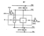
これまでは、部品の使用状態に応じてリーク電流を遮断する方法を説明してきた。部品によっては、他の方法と組み合わせることにより、さらに大きく電力を低減できる場合がある。その例を示したのが図7、図8である。図7はクロックに同期して動作する回路ブロックなどの部品において、上記のリーク電流の遮断とクロック信号の遮断を合わせて用いた例である。同期型の回路ブロックは、通常入力データをラッチするフリップフロップFFと、論理回路Lとを単位として構成される。M1およびM2は、それぞれPチャネルMOSトランジスタ、NチャネルMOSトランジスタであり、電源スイッチとして動作する。これらのMOSトランジスタは電源スイッチとして動作するので、論理回路Lで使用されるMOSトランジスタのしきい値電圧の絶対値に比較してそのしきい電圧の絶対値を大きく設定することが望ましい。または、/φSW1やφSW2の振幅を調整してオフ時にゲートソース電圧を負電位にすることにより、電源スイッチがオフ状態のときにリーク電流が十分に小さくなるように設計してもよい。なお、図7,8の実施例では、他の回路と同様のプロセスで形成できるという利点のために、電源スイッチとしてMOSトランジスタを用いるが、完全にリーク電流を遮断したい場合には、例えば半導体チップの外部に設けた機械的なスイッチを用いるなど必要に応じて他の手段でスイッチを形成してもよい。
【0029】
ゲートG1はクロック信号CLKを入力するか遮断するかを制御するための回路、ゲートG2は電源スイッチがオフした際に論理回路の出力信号がフローティング状態になることを防止する回路である。これらG1,G2の回路は電力制御ユニットPCUに設ければよい。基本的な動作は以下の通りである。
【0030】
まず、ステート信号φST−iが「L」レベルになると、ゲートG1はクロック信号CLKのフリップフロップFFへの入力を遮断する。また、前述のようにスイッチ制御信号/φSW1とφSW2がそれぞれ「H」レベル、「L」レベルに遷移し、電源スイッチがオフする。これにより、クロック入力とリーク電流の両方が遮断されるので消費電力の削減効果が大きい。図面ではクロックが入力されるフリップフロップFFは一つしか記載していないが実際は多数ある。したがってクロック入力が停止することによる電力削減効果は大きい。なお、ゲートG2により、ステート信号φST−iが「L」レベルになると論理回路の出力OUTが固定されるため、次段の回路の入力がフローティングになることによるリーク電流(いわゆる貫通電流)を防止することができる。つづいて、タスクの継続時間から予熱時間を引いた時間が経過すると、電源スイッチM1, M2はオン状態となる。タスクが終了するとステート信号φST−iが「H」レベルになり、クロック信号CLKの遮断と出力信号の固定を終了し、この部品の動作が始まる。ここで、クロック信号の入力においては電源スイッチのように長い予熱時間が不要なのでステート信号φST−iをゲートG1に入力して制御している。以上のように本実施例では、タスク継続時間を利用して、電源スイッチとクロック入力を同時に制御することにより、電力削減の効果を大きくしている。
【0031】
図8は、2次キャッシュのようなメモリに対して本発明を適用した例である。図8において、CDEC, TGEN, DEC, ARY, AMP−IOはそれぞれ、コマンドデコーダ、タイミングジェネレータ、デコーダ、メモリアレイ、センスアンプ及び入出力回路である。また、ADD, CMD, DI, DOは、アドレス、コマンド、入力データ、出力データを示す。なお、説明の都合上、これらの記号を、信号そのものとして扱う場合とそれらの入力線または出力線として扱う場合がある。また、図では煩雑になるため複数の信号線を1本で描いている。M1, M2, M11, M12, M21, M22はMOSトランジスタからなる電源スイッチであり、M1, M2は部品全体を電源から遮断する電源スイッチ、M11, M21は、デコーダDECを電源から遮断する電源スイッチ、 M12, M22はセンスアンプ及び入出力回路AMP−IOを電源から遮断する電源スイッチである。
【0032】
図8では、部品を電源から遮断する電源スイッチと部品の要素回路を選択的に電源から遮断する電源スイッチとを設けてある。これにより、部品が不使用状態にあるときに部品全体のリーク電流を遮断することに加えて、部品が使用状態であるときにも動作にあわせて選択的に要素回路を電源から遮断できる。したがって、リーク電流の低減効果をより大きくすることが可能となる。具体的には、ステート信号φST−iが「L」レベルのときにはMOSトランジスタM1, M2をオフとする。ステート信号φST−iが「H」レベルのときには、MOSトランジスタM1, M2はオンしているが、デコーダDECやセンスアンプ及び入出力回路AMP−IOを活性化する必要のないときにはMOSトランジスタM11, M21あるいは、MOSトランジスタM12,M22をオフにする。一般にメモリでは、アドレスやコマンドが入力されて読み出し、あるいは書き込みが行なわれて次のアドレスやコマンドを入力するまでの時間をサイクル時間と呼ぶ。このサイクル時間常にデコーダDECやセンスアンプ及び入出力回路AMP−IOが動作しているわけではなく、タイミングジェネレータTGENが管理する一定の時間だけ動作する。したがって、タイミングジェネレータTGENの制御により、使用されない時間においては電源スイッチによりリーク電流を遮断することが可能である。
【0033】
なお、図8の例ではメモリアレイARYに個別にスイッチを設けていない。これは、2次キャッシュなどではSRAMなどの揮発性メモリセルで構成されるために電源を遮断するとデータが失われてしまうからである。しかし、この場合でも、電源を完全にオフせずに、データが失われない程度に電流を絞ることは可能である。あるいは、メモリセルとして強誘電体メモリやマグネティックメモリなどの不揮発メモリセルを利用すれば、電流を遮断してもデータは保持される。また、メモリ全体のリーク電流を遮断するスイッチM1とM2はメモリアレイも含んで電源を遮断するが、これはタスクが切り替わった時にはこのメモリのデータを失ってもよい場合に限られる。もしも、タスク切換え時にもデータを保持する必要がある場合には、メモリアレイARYは電源に常時接続するように構成することができる。さらに、個別のスイッチを設ける要素回路はデコーダDECやセンスアンプ及び入出力回路AMP−IOに限られず、他の要素部品に設けることも可能であり、必要に応じて様々な変形が可能である。
【0034】
なお、これまでは、半導体装置の動作時におけるリーク電流の低減方法について記載したが、半導体装置の待機時において電源スイッチを遮断して電力の削減を図ることができることはもちろんである。半導体装置全体が待機時から動作時に移行する場合には多少の遅延は許容される場合が多いので、予熱時間を見込んであらかじめスイッチをオンしておく必要はない。
【0035】
【発明の効果】
本発明により、集積回路の動作状態におけるリーク電流を効果的に低減することができる。
【図面の簡単な説明】
【図1】本発明の半導体装置のブロック図である。
【図2】部品毎のステート信号の遷移の例である。
【図3】電力制御ユニットの入出力信号を示す図である。
【図4】タスクの期間中におけるスイッチ制御のタイミングを示す図である。
【図5】割り込み処理が生じた時のスイッチ制御のタイミングを示す図である。
【図6】スイッチ制御のための信号のタイミングを示す図である。
【図7】本発明による半導体装置内部の論理ブロックの構成を示す図である。
【図8】本発明による半導体装置内部のメモリブロックの構成を示す図である。
【符号の説明】
CHIP−−−チップ、CPU −−−CPUコア、DSP −−−DSPコア、I−C−−−命令キャッシュ、D−C−−−データキャッシュ、XY−M−−−XYメモリ、2ND−C−−−2次キャッシュ、DMAC−−−ダイレクトメモリアクセス制御回路、PER−IP−−−周辺IPコア、BC−−−バス制御回路、TID−R−−−タスクIDレジスタ、RM−R−−−リソ−ス管理レジスタ、ST−DEC−−−ステートデコーダ、PCU−−−電力制御ユニット、I−BUS−−−命令バス、D−BUS−−−データバス、P−BUS1−−−第一周辺バス、P−BUS2−−−第二周辺バス、CDEC−−−コマンドデコーダ、TGEN−−−タイミングジェネレータ、DEC−−−デコーダ、ARY−−−メモリアレイ、AMP−IO−−−センスアンプ及び入出力回路、ADD−−−アドレス、CMD−−−コマンド、DI−−−入力データ、DO−−−出力データ、FF−−−フリップフロップ、L−−−論理回路、SW1, SW2−−−電源スイッチ、M1, M2, M11, M12, M21, M22−−−MOSトランジスタで構成される電源スイッチ、Vdd−−−高電位側の電源、Vss−−−低電位側の電源、T−task−−−タスク継続時間、T−off−−−電源スイッチ遮断時間、T−min−−−電源スイッチオフの最低有効時間、T−heat−−−予熱時間。[0001]
TECHNICAL FIELD OF THE INVENTION
The present invention relates to a semiconductor device including a semiconductor integrated circuit in which a CPU core, a logic core, a memory core, and the like are integrated.
[0002]
[Prior art]
With the scaling of MOS transistors, both the speed and power of semiconductor integrated circuits have been improved. However, in a recent semiconductor integrated circuit using a MOS transistor having a processing size of about 0.15 μm or less, it is becoming difficult to achieve both speed and power performance with scaling of a power supply voltage. This is because setting the threshold voltage of the MOS transistor low in order to secure the speed at a low power supply voltage causes an increase in the sub-threshold leakage current.
[0003]
Most of current semiconductor integrated circuits use CMOS circuits. This is because, ideally, the AC current accompanying the charging / discharging of the load capacitance flows only during the operation of the CMOS circuit, and no current flows during standby. However, the sub-threshold leakage current always flows as a DC current. Since the sub-threshold leak current increases as the threshold voltage of the MOS transistor decreases, in a CMOS circuit using a MOS transistor with a low threshold voltage, the deterioration of the power performance due to the sub-threshold leak current is not negligible.
[0004]
As a conventional technique for reducing the sub-threshold leakage current, a method has been proposed in which a power switch including a MOS transistor having a high threshold voltage is provided between a circuit and a power supply line, and the MOS transistor is turned off during standby. For example, the method described in the proceedings of the International Solid-State Device Conference (ISSCC) held in San Francisco in the United States in February 1998, pages 192 to 193 (first prior art), or JP-A-10-208473 ( The method described in the second prior art) is an example.
[0005]
[Problems to be solved by the invention]
In the first prior art, a sub-threshold leak power supply (hereinafter, referred to as “leak current”) is shut off by a power switch when the semiconductor device is on standby.
[0006]
However, when the MOS transistor is further miniaturized and the power supply voltage is reduced to, for example, 1 V or less, the threshold voltage must be set lower. As a result, the leakage current further increases, while the AC current during operation decreases in proportion to the power supply voltage. As a result, it is expected that the ratio of the leakage current to the consumption current during the operation will increase, and the magnitude of the leakage current as compared with the magnitude of the AC current during the operation cannot be ignored.
[0007]
The second prior art describes that a power switch is turned off for an unused circuit block even during operation. However, there are the following two problems when trying to realize current interruption by the power switch during operation.
[0008]
The first problem is that if the power switch is turned on and off unnecessarily, the current consumption increases. Even during operation, the entire integrated circuit does not always operate. Therefore, it is possible to cut off the current for unused circuit blocks by the power switch. However, if the power switch is repeatedly turned on and off within a short time, the transient current consumed when the power switch is turned on may be larger than the reduction of the leak current due to the cutoff of the power switch. .
[0009]
The second problem is that the speed of the integrated circuit is reduced by turning on / off the power switch. It takes time (hereinafter, referred to as "preheating time") from when the power switch is turned on to when the circuit whose current has been interrupted can be used. Therefore, in some cases, the speed of the entire integrated circuit may be significantly reduced.
[0010]
[Means for Solving the Problems]
In order to solve the above problems, the present invention uses the following means. In order to solve the first problem, power switch control is performed using the duration of a task of a processor (CPU) that controls an integrated circuit. Specifically, the power supply switch that supplies current to unused circuit blocks is turned off by referring to a task ID register and a resource management register inside the CPU. Although it depends on the circuit size, the current reduction effect by cutting off the leakage current is generally effective when the power switch can be turned off for several microseconds or more, compared to the current consumption by turning the power switch on and off. is there. On the other hand, since the duration of a task is usually about 1 millisecond, the above problem can be solved by managing the power switch based on the duration of the task. As for the second problem, after a certain time has elapsed after the power switch is turned off, the power switch is turned on before the next task starts. If this fixed time is set to be less than the time obtained by subtracting the preheating time (the time required to charge the pseudo power supply line) from the duration of the task, the preheating time has expired before the next task starts. To avoid delaying the next task.
[0011]
BEST MODE FOR CARRYING OUT THE INVENTION
Hereinafter, embodiments of the present invention will be described with reference to the drawings.
[0012]
FIG. 1 shows a basic configuration when the present invention is applied to a semiconductor integrated circuit in which a CPU core, a DSP core, various logic cores, a memory core, and the like are integrated on one chip. The present invention is not limited to a semiconductor integrated circuit in the form of one chip as shown in FIG. 1, but a system or board on which a plurality of chips are mounted or a so-called multi-chip package in which a plurality of chips are integrated in one package. And the combination thereof. For simplicity, the following description is based on a one-chip configuration as shown in FIG.
[0013]
In FIG. 1, a silicon chip CHIP includes, as main cores, a CPU core CPU, a DSP core DSP, an instruction cache IC, a data cache DC, an XY memory XY-M, a secondary cache 2ND-C, and a direct memory access control. It includes a circuit DMAC, a peripheral IP core PER-IP, and a bus control circuit BC. The task ID register TID-R is a register inside the CPU core, which is a register for managing each task, and the resource management register RM-R is a register for managing resources (cores) to be used. . Also, a power control unit PCU is provided for each resource (core) as a unit for performing power control, and the state decoder ST-DEC sends a state signal φST indicating whether or not to use each resource (core) to the power control unit PCU. send.
[0014]
Further, I-BUS, D-BUS, P-BUS1, and P-BUS2 are an instruction bus, a data bus, a first peripheral bus, and a second peripheral bus, respectively.
[0015]
1, various cores including a CPU core, a memory, a bus, and the like are shown as examples of basic units constituting a chip for digital processing (hereinafter, these circuit blocks, A basic unit such as a memory is referred to as a component.) Since the operations of these components are assumed to be general, the description of the functions is omitted here. According to the present invention, during operation of a semiconductor device, a power supply switch of an unused component is turned off to reduce leakage current. First, based on the contents of the task ID register TID-R inside the CPU core and the resource management register RM-R for managing resources (parts) to be used, the state decoder ST-DEC uses the state decoder ST-DEC for each part. A state signal φST indicating whether or not to perform is transmitted. In each component, power control unit PCU detects whether or not the component is used based on state signal φST, and when not used, shuts off power from a power switch provided inside power control unit PCU.
[0016]
In the configuration shown in FIG. 1, the power control unit PCU is not added to the CPU core, the data cache DC as its primary cache, and the instruction cache IC. This is because there is not much time during which these power supplies can be shut off during operation. As for other components, it is possible not to add the power control unit PCU for a component having a short period of shutting off the power.
[0017]
Hereinafter, the power control operation of the present invention will be described with reference to FIGS. FIG. 2 is an example of the state signal φST output from the state decoder ST-DEC. In the present embodiment, the number of components to be controlled for leakage current is n, and state signals indicating whether or not to use each of them are indicated by φST-1 to φST-n. A, B,..., F in the horizontal columns indicate the tasks of the CPU, and the components used differ depending on the tasks. In this example, when the state signal φST-i is “H” (high level), it indicates that the component is used, and when it is “L” (low level), it means that it is not used. . For example, the
[0018]
As described above, the state signal φST signal is transmitted to the power control unit PCU of each component, and the power control unit PCU controls the power switch. FIG. 3 shows a specific configuration example of the power control unit PCU. The power switch SW1 is provided between the power supply Vdd on the high potential side and the circuit LG configuring the controlled component i, and the power switch SW2 is provided between the power supply Vss on the low potential side and the circuit LG configuring the controlled component i (here, the circuit LG). Although one inverter is shown for simplicity, the present invention is not limited to this, and it is needless to say that the inverter is a circuit necessary for the function of the controlled component. A CMOS inverter circuit is illustrated as the circuit LG. The power switch control circuit SWC controls the power switches SW1 and SW2. φack and φRESET are a signal indicating that the preheating time has ended after the power switches SW1 and SW2 are turned on, and a reset signal for resetting the power switch control halfway. When the state signal φST-i becomes “L”, the power switch control circuit SWC turns off the power switches SW1 and SW2. Thereby, the leak current between the power supply and the component i is cut off.
[0019]
In the example of FIG. 3, the power switch SW is provided on both the high-potential-side power supply Vdd and the low-potential-side power supply Vss. However, if there is no current leakage path inside the circuit constituting the component, either one of them is provided. It is also possible to simply provide a power switch. In that case, the occupied area is reduced, and the power for turning on and off the power switch can be reduced.
[0020]
The basic operation of the power control unit PCU in FIG. 3 will be described with reference to FIG. FIG. 4 shows the operation of the power control unit PCU of the component i when the state signal φST-i for the component i becomes “L” level, that is, during the task duration T-task in which the component i is not used. is there.
[0021]
First, when the state signal φST-i becomes “L” level, the power control unit PCU turns off the power switch of the component i. Thereafter, when the time T-off (the time T-off means a switch-off period) elapses, the power control unit PCU turns on the switch (SW-on) and connects the component i to the power supply. Here, the time T-off is set so as not to exceed a time obtained by subtracting the preheating time T-heat of the component i from the task duration T-task. The preheating time T-heat is a time required to charge the pseudo power supply lines Vdd 'and Vss' of the circuit LG. Thereby, since the preheating has been completed at the time when the task is completed, it is possible to avoid the occurrence of a waiting time when using the component i in the next task. The preheating time differs depending on the component configuration and the circuit scale. Therefore, it is desirable to set the T-off time for each component. Therefore, the power control unit PCU has a built-in ring oscillator circuit and a counter for adding the output pulse, and operates the ring oscillator and the counter at the same time as the power switch is turned off, and the value of the counter is set to a value set in advance for each component. If it exceeds, a method such as turning on a power switch can be used.
[0022]
On the other hand, as described above, if the power switch is turned on and off in a short time, the current for driving the power switch may be larger due to the effect of reducing the leak current by turning off the power switch. Assuming that the minimum effective period of the switch-off is defined as T-min, which is defined as a switch-off period in which the power consumption reduced by the reduction of the leakage current and the power consumption by driving the power switch are equal to T-off. Must be bigger. In addition, since it is necessary to turn on the switch in advance for the preheating time as described above, T-off is eventually
T-min ≦ T-off ≦ T-task T-heat (1)
Need to satisfy the relationship. The value of the minimum effective period T-min varies depending on the size of the leak current, the size of the switch, and the like, but is usually about several tens of microseconds, and the T-heat is also about several tens of microseconds. On the other hand, the task duration T-task is usually on the order of milliseconds. Therefore, if the switch is controlled based on the task as in the present invention, the relationship (1) can be easily satisfied. The minimum effective period T-min and the preheating time T-heat can be estimated in advance by simulation based on circuit analysis or by calculation based on circuit constants. Therefore, when determining how many units, such as a circuit and a memory, are to be defined as “parts” when designing a semiconductor device, it is only necessary to design so as to satisfy (1). In the example of FIG. 1, components are defined for each function. However, cores having different functions (for example, a plurality of peripheral IP cores) can be collectively defined as one component and controlled by a common power switch. It is. It is desirable that a circuit block that cannot satisfy the condition (1) is always connected to a power supply without providing the power supply control unit PCU.
[0023]
In the example of FIG. 4, the power switch is automatically turned on when a certain time (T-off) elapses after the power switch is turned off. In this way, the delay due to the preheating time T-heat can be concealed. However, if the component is not used in the next task, the power switch is turned off again so that the current consumption for turning on the power switch is reduced. Is wasted. If this causes a problem, it is determined that the power supply switch is not turned on if the use or non-use in the next task is determined first by referring to the task ID register TID-R of the CPU and the next task is not used. Control may be performed.
[0024]
On the other hand, when an interrupt operation occurs, the task is aborted halfway, so control corresponding to the interrupt operation is required. For example, even if an interrupt occurs when the state signal φST-i is in an unused state for a certain component and the current task is terminated, there is no particular problem in the case where the next task is not used as it is. In this case, the power switch may be turned on at the time when the remaining heat time T-heat is subtracted from the time when the new task is completed by continuing to shut off the power switch. However, when an interrupt occurs and the component is used in the next task, control as shown in FIG. 5 is required.
[0025]
First, when the φRESET signal is activated to “H” in response to the interrupt, the power switch control sequence is reset and the power switch is turned on (SW-on). Subsequently, the acknowledgment signal φack for notifying the end of the preheating is activated to “H”, and the next task task (2) is started. In the case where the interruption is performed as described above, a delay occurs by the amount of the preheating time T-heat. Actually, there are a plurality of parts, and the required preheating time differs for each part. Therefore, the CPU may start the next task after acknowledgment signals φack from all components used after the interruption are activated.
[0026]
FIG. 6 is a time chart showing transition of each signal in the continuous tasks A, B, C, and D for the component i. In this time chart, the polarities of the signals φSW1 and φSW2 for controlling the power switch are reversed. φSW1 is “L” to turn on the power switch, “H” to turn off the power switch, φSW2 is “L” to turn off the power switch, and “H” to turn on the power switch. To indicate this, the notation of φSW1 is “/ φSW1”.
[0027]
In FIG. 6, the state signal φST-i is “L”, “H”, “L”, and “H” for tasks A, B, C, and D, respectively. In other words, in this embodiment, the state of the component i is changed to unused, used, not used, and used. First, the control shown in FIG. First, in order to turn off the power switch, / φSW1 and φSW2 are changed to “H” and “L”, respectively, to cut off the leak current. The power supply switch is turned on by returning the potentials of φSW1 and φSW2 to the original state before the preheating time T-heat before the time when the task A ends. Subsequently, in task B, the state signal φSW-i transitions to “H”, and the component i enters the use state. At this time, since the preheating has been completed during the previous task A, the task B can be started without a delay time. Subsequently, in the task C, the state signal φSW-i transitions to “L” again, and the component i enters an unused state. In this example, an interrupt occurs in this state, and the task is switched to the task D in a shorter time than the normal task duration. In this case, the control shown in FIG. 5 is performed. φRESET is input, and the potentials of / φSW1 and φSW2 are changed to “L” and “H”, respectively, to turn on the power switch. Thereafter, when the preheating time T-heat has elapsed, the acknowledge signal φack changes to “H”. When the acknowledgment signals φack of the other components that change from the unused state to the used state are all switched, the CPU executes the next task, task D. As described above, according to the power control of the present invention, it is possible to cut off the leak current of the unused component without causing a delay time during the normal operation. Further, even when an interrupt occurs, it is possible to confirm that the preheating has been completed and to proceed to the next task, so that no malfunction occurs.
[0028]
So far, a method of interrupting a leak current according to the use state of a component has been described. In some parts, the power can be further reduced by combining with other methods. 7 and 8 show such examples. FIG. 7 shows an example in which the above-described cutoff of the leak current and the cutoff of the clock signal are used together in a component such as a circuit block operating in synchronization with the clock. The synchronous circuit block is generally configured with a flip-flop FF that latches input data and a logic circuit L as a unit. M1 and M2 are a P-channel MOS transistor and an N-channel MOS transistor, respectively, and operate as a power switch. Since these MOS transistors operate as power switches, it is desirable to set the absolute value of the threshold voltage larger than the absolute value of the threshold voltage of the MOS transistor used in the logic circuit L. Alternatively, the leakage current may be designed to be sufficiently small when the power switch is off by adjusting the amplitude of / φSW1 or φSW2 to make the gate-source voltage negative when off. In the embodiment shown in FIGS. 7 and 8, a MOS transistor is used as a power switch because of the advantage that it can be formed by the same process as other circuits. The switch may be formed by other means as needed, such as by using a mechanical switch provided outside the device.
[0029]
The gate G1 is a circuit for controlling whether to input or cut off the clock signal CLK, and the gate G2 is a circuit for preventing the output signal of the logic circuit from being in a floating state when the power switch is turned off. These G1 and G2 circuits may be provided in the power control unit PCU. The basic operation is as follows.
[0030]
First, when the state signal φST-i becomes “L” level, the gate G1 cuts off the input of the clock signal CLK to the flip-flop FF. Also, as described above, the switch control signals / φSW1 and φSW2 transition to “H” level and “L” level, respectively, and the power switch is turned off. As a result, both the clock input and the leak current are cut off, so that the effect of reducing power consumption is great. Although only one flip-flop FF to which a clock is input is shown in the drawing, there are actually many flip-flops. Therefore, the power reduction effect by stopping the clock input is great. Note that when the state signal φST-i goes to “L” level, the output OUT of the logic circuit is fixed by the gate G2, so that a leakage current (a so-called through current) caused by the input of the next-stage circuit becoming floating is prevented. can do. Subsequently, when the time obtained by subtracting the preheating time from the task duration time elapses, the power switches M1 and M2 are turned on. When the task is completed, the state signal φST-i becomes “H” level, the cutoff of the clock signal CLK and the fixing of the output signal are completed, and the operation of this component is started. Here, the input of the clock signal does not require a long preheating time like a power switch, so that the state signal φST-i is input to the gate G1 for control. As described above, in this embodiment, the power reduction effect is increased by simultaneously controlling the power switch and the clock input using the task duration.
[0031]
FIG. 8 shows an example in which the present invention is applied to a memory such as a secondary cache. In FIG. 8, CDEC, TGEN, DEC, ARY, and AMP-IO are a command decoder, a timing generator, a decoder, a memory array, a sense amplifier, and an input / output circuit, respectively. ADD, CMD, DI, and DO indicate an address, a command, input data, and output data. For the sake of explanation, these symbols may be treated as signals themselves or as their input lines or output lines. In addition, in the figure, a plurality of signal lines are drawn by one for simplicity. M1, M2, M11, M12, M21, M22 are power switches composed of MOS transistors, M1 and M2 are power switches for shutting off the whole components from the power source, M11 and M21 are power switches for shutting off the decoder DEC from the power source, M12 and M22 are power switches that shut off the sense amplifier and the input / output circuit AMP-IO from the power supply.
[0032]
In FIG. 8, a power switch for shutting off a component from a power source and a power switch for selectively shutting off a component circuit of the component from the power source are provided. Thus, in addition to shutting off the leak current of the entire component when the component is not in use, the element circuit can be selectively shut off from the power supply in accordance with the operation when the component is in use. Therefore, it is possible to further increase the effect of reducing the leak current. Specifically, when state signal φST-i is at “L” level, MOS transistors M1 and M2 are turned off. When the state signal φST-i is at the “H” level, the MOS transistors M1 and M2 are on, but when it is not necessary to activate the decoder DEC, the sense amplifier and the input / output circuit AMP-IO, the MOS transistors M11 and M21 Alternatively, the MOS transistors M12 and M22 are turned off. Generally, in a memory, the time from when an address or command is input and read or write is performed until the next address or command is input is called a cycle time. This cycle time does not mean that the decoder DEC, the sense amplifier, and the input / output circuit AMP-IO always operate, but operate only for a certain time managed by the timing generator TGEN. Therefore, under the control of the timing generator TGEN, it is possible to cut off the leak current by the power switch during the unused time.
[0033]
Note that, in the example of FIG. 8, no switch is individually provided in the memory array ARY. This is because data is lost when the power is cut off because the secondary cache is constituted by volatile memory cells such as SRAMs. However, even in this case, it is possible to reduce the current to the extent that data is not lost without completely turning off the power. Alternatively, if a non-volatile memory cell such as a ferroelectric memory or a magnetic memory is used as a memory cell, data is retained even when current is cut off. The switches M1 and M2 for shutting off the leak current of the entire memory shut off the power including the memory array, but only when the data in the memory may be lost when the task is switched. If it is necessary to retain data even at the time of task switching, the memory array ARY can be configured to be constantly connected to a power supply. Further, the element circuits provided with the individual switches are not limited to the decoder DEC, the sense amplifier, and the input / output circuit AMP-IO, but can be provided in other element parts, and various modifications can be made as necessary.
[0034]
Although a method of reducing leakage current during operation of a semiconductor device has been described above, it goes without saying that power can be reduced by shutting off a power switch during standby of the semiconductor device. When the entire semiconductor device shifts from standby to operation, a slight delay is often allowed, so that it is not necessary to turn on the switch in advance in consideration of the preheating time.
[0035]
【The invention's effect】
According to the present invention, a leak current in an operation state of an integrated circuit can be effectively reduced.
[Brief description of the drawings]
FIG. 1 is a block diagram of a semiconductor device of the present invention.
FIG. 2 is an example of transition of a state signal for each component.
FIG. 3 is a diagram showing input / output signals of a power control unit.
FIG. 4 is a diagram showing switch control timing during a task period.
FIG. 5 is a diagram illustrating switch control timing when an interrupt process occurs.
FIG. 6 is a diagram illustrating timings of signals for switch control.
FIG. 7 is a diagram showing a configuration of a logic block inside a semiconductor device according to the present invention.
FIG. 8 is a diagram showing a configuration of a memory block inside a semiconductor device according to the present invention.
[Explanation of symbols]
CHIP --- chip, CPU --- CPU core, DSP --- DSP core, IC --- instruction cache, DC --- data cache, XY-M --- XY memory, 2ND-C --- Secondary cache, DMAC--Direct memory access control circuit, PER-IP--Peripheral IP core, BC--Bus control circuit, TID-R--Task ID register, RM-R-- -Resource management register, ST-DEC-State decoder, PCU-Power control unit, I-BUS-Instruction bus, D-BUS-Data bus, P-BUS1--First Peripheral bus, P-BUS2-second peripheral bus, CDEC--command decoder, TGEN--timing generator, DEC--decoder, ARY--memory array, MP-IO-sense amplifier and input / output circuit, ADD--address, CMD--command, DI--input data, DO---output data, FF---flip-flop, L---- Logic circuit, SW1, SW2--power switch, M1, M2, M11, M12, M21, M22-power switch composed of MOS transistors, Vdd---high-potential power supply, Vss---low Potential side power supply, T-task--task duration, T-off--power switch off time, T-min--minimum effective time of power switch off, T-heat-preheating time.
Claims (9)
すくなくとも一つの第1回路ブロックを含む複数の回路ブロックと、
上記少なくとも一つの第1回路ブロックのそれぞれに対応して設けられ、上記電源線から上記第1回路ブロックへの電源の供給を制御する少なくとも一つのスイッチと、
上記複数の回路ブロックの少なくとも一つを使用状態としてタスクを実行するプロセッサとを有し、
上記プロセッサのタスクの実行において、上記第1回路ブロックはその不使用状態への移行を指示するステート信号を受けて対応する上記スイッチをオフ状態とし、上記第1回路ブロックがその使用状態への移行を指示するステート信号を受けるのに先立って上記スイッチをオン状態とする半導体装置。Power line,
A plurality of circuit blocks including at least one first circuit block;
At least one switch provided corresponding to each of the at least one first circuit block and controlling supply of power from the power supply line to the first circuit block;
A processor that executes a task with at least one of the plurality of circuit blocks in use,
In executing the task of the processor, the first circuit block receives the state signal instructing the transition to the non-use state, turns off the corresponding switch, and the first circuit block transitions to the use state. A semiconductor device that turns on the switch before receiving a state signal instructing the switch.
上記複数の回路ブロックは、上記電源線とスイッチを介さず接続される少なくとも一つの第2の回路ブロックを有する半導体装置。In claim 1,
A semiconductor device, wherein the plurality of circuit blocks include at least one second circuit block connected to the power supply line without a switch.
上記第1回路ブロックが上記スイッチをオフ状態とする時間T−offは、T−off<タスク継続時間T−task−予熱時間T−heatの関係を満たし、
上記予熱時間T−heatは、上記第1回路ブロックの少なくとも回路規模に応じて決定される半導体装置。In claim 1,
The time T-off at which the first circuit block turns off the switch satisfies the relationship of T-off <task duration time T-task-preheating time T-heat,
The semiconductor device, wherein the preheating time T-heat is determined according to at least a circuit size of the first circuit block.
上記第1回路ブロックが上記スイッチをオフ状態とする時間T−offは、時間T−min< T−offの関係を満たし、
上記時間T−minは、上記第1回路ブロックのサブスレッショルド電流による消費電力と電源スイッチを駆動するための消費電力とに応じて決定される半導体装置。In claim 1,
The time T-off at which the first circuit block turns off the switch satisfies the relationship of time T-min <T-off,
The semiconductor device according to claim 1, wherein the time period T-min is determined according to power consumption by a subthreshold current of the first circuit block and power consumption for driving a power switch.
上記第1回路ブロックは、クロック信号の入力に応じてそのデータを入出力するフリップフロップと、
上記フリップフロップの出力を受ける論理回路と、
第1のゲート回路とを有し、
上記プロセッサのタスクの実行において、上記第1のゲート回路は上記第1回路ブロックの不使用状態への移行を指示するステート信号を受けて、上記クロック信号の上記フリップフロップへの入力を遮断する半導体装置。In claim 1,
The first circuit block includes a flip-flop that inputs and outputs data according to a clock signal input;
A logic circuit receiving the output of the flip-flop;
A first gate circuit;
In performing the task of the processor, the first gate circuit receives a state signal instructing a transition of the first circuit block to an unused state, and cuts off input of the clock signal to the flip-flop. apparatus.
第2のゲート回路を有し、
上記プロセッサのタスクの実行において、上記第2のゲート回路は上記第1回路ブロックの不使用状態への移行を指示するステート信号を受けて、上記論理回路の出力を所定のレベルに制御する半導体装置。In claim 5,
A second gate circuit,
A semiconductor device for controlling the output of the logic circuit to a predetermined level in response to a state signal instructing a transition of the first circuit block to a non-use state in executing the task of the processor; .
上記第1回路ブロックは複数の要素回路により構成され、
上記複数の要素回路の少なくとも一つは個別に電力の供給が制御可能である半導体装置。In claim 1,
The first circuit block includes a plurality of element circuits,
A semiconductor device in which at least one of the plurality of element circuits can individually control power supply.
すくなくとも一つの第1回路ブロックを含む複数の回路ブロックと、
上記少なくとも一つの第1回路ブロックのそれぞれに対応して設けられ、上記電源線から上記第1回路ブロックへの電源の供給を制御する少なくとも一つのスイッチと、
上記複数の回路ブロックの少なくとも一つを使用状態としてタスクを実行するプロセッサとを有し、
上記プロセッサのタスクの実行において、上記第1回路ブロックはその不使用または使用状態への移行を指示するステート信号に応じて上記スイッチを制御する半導体装置。Power line,
A plurality of circuit blocks including at least one first circuit block;
At least one switch provided corresponding to each of the at least one first circuit block and controlling supply of power from the power supply line to the first circuit block;
A processor that executes a task with at least one of the plurality of circuit blocks in use,
In the semiconductor device, the first circuit block controls the switch according to a state signal instructing a transition to a non-use state or a use state when the processor performs a task.
すくなくとも一つの第1回路ブロックを含む複数の回路ブロックと、
上記少なくとも一つの第1回路ブロックのそれぞれに対応して設けられ、上記電源線から上記第1回路ブロックへの電源の供給を制御する少なくとも一つのスイッチと、
上記複数の回路ブロックの少なくとも一つを使用状態としてタスクを実行するプロセッサとを有し、
上記スイッチはタスクの継続時間を単位に制御される半導体装置。Power line,
A plurality of circuit blocks including at least one first circuit block;
At least one switch provided corresponding to each of the at least one first circuit block and controlling supply of power from the power supply line to the first circuit block;
A processor that executes a task with at least one of the plurality of circuit blocks in use,
A semiconductor device in which the switch is controlled in units of task duration.
Priority Applications (4)
| Application Number | Priority Date | Filing Date | Title |
|---|---|---|---|
| JP2002175170A JP2004021574A (en) | 2002-06-17 | 2002-06-17 | Semiconductor device |
| US10/373,042 US7023757B2 (en) | 2002-06-17 | 2003-02-26 | Semiconductor device |
| US11/363,060 US7254082B2 (en) | 2002-06-17 | 2006-02-28 | Semiconductor device |
| US11/826,854 US20080016383A1 (en) | 2002-06-17 | 2007-07-19 | Semiconductor device |
Applications Claiming Priority (1)
| Application Number | Priority Date | Filing Date | Title |
|---|---|---|---|
| JP2002175170A JP2004021574A (en) | 2002-06-17 | 2002-06-17 | Semiconductor device |
Publications (2)
| Publication Number | Publication Date |
|---|---|
| JP2004021574A true JP2004021574A (en) | 2004-01-22 |
| JP2004021574A5 JP2004021574A5 (en) | 2005-09-22 |
Family
ID=29728018
Family Applications (1)
| Application Number | Title | Priority Date | Filing Date |
|---|---|---|---|
| JP2002175170A Pending JP2004021574A (en) | 2002-06-17 | 2002-06-17 | Semiconductor device |
Country Status (2)
| Country | Link |
|---|---|
| US (3) | US7023757B2 (en) |
| JP (1) | JP2004021574A (en) |
Cited By (7)
| Publication number | Priority date | Publication date | Assignee | Title |
|---|---|---|---|---|
| JP2008181329A (en) * | 2007-01-24 | 2008-08-07 | Matsushita Electric Ind Co Ltd | Semiconductor integrated circuit and its power supply control method |
| JP2009151573A (en) * | 2007-12-20 | 2009-07-09 | Fujitsu Microelectronics Ltd | Semiconductor integrated circuit |
| JP2009231360A (en) * | 2008-03-19 | 2009-10-08 | Fujitsu Ltd | Semiconductor device |
| JP2012009587A (en) * | 2010-06-24 | 2012-01-12 | Fujitsu Ltd | Semiconductor device and method of controlling semiconductor device |
| JP2012069115A (en) * | 2004-07-27 | 2012-04-05 | Intel Corp | Power management coordination in multi-core processor |
| JP2013093038A (en) * | 2007-06-27 | 2013-05-16 | Qualcomm Inc | Power gating for multimedia processing power management |
| JP2014142719A (en) * | 2013-01-22 | 2014-08-07 | Canon Inc | Information processing device |
Families Citing this family (14)
| Publication number | Priority date | Publication date | Assignee | Title |
|---|---|---|---|---|
| JP2003132683A (en) | 2001-10-23 | 2003-05-09 | Hitachi Ltd | Semiconductor device |
| JP4387815B2 (en) * | 2004-01-30 | 2009-12-24 | 富士通株式会社 | Serial type interface circuit, power saving method thereof, and device having serial interface |
| KR100571646B1 (en) * | 2005-03-31 | 2006-04-17 | 주식회사 하이닉스반도체 | Semiconductor device with power down mode |
| JP4621113B2 (en) * | 2005-10-28 | 2011-01-26 | ルネサスエレクトロニクス株式会社 | Semiconductor integrated circuit device |
| JP2007226632A (en) * | 2006-02-24 | 2007-09-06 | Denso Corp | Microcomputer |
| US9411390B2 (en) * | 2008-02-11 | 2016-08-09 | Nvidia Corporation | Integrated circuit device having power domains and partitions based on use case power optimization |
| US8575993B2 (en) * | 2011-08-17 | 2013-11-05 | Broadcom Corporation | Integrated circuit with pre-heating for reduced subthreshold leakage |
| US9471395B2 (en) | 2012-08-23 | 2016-10-18 | Nvidia Corporation | Processor cluster migration techniques |
| US20140062561A1 (en) | 2012-09-05 | 2014-03-06 | Nvidia Corporation | Schmitt receiver systems and methods for high-voltage input signals |
| US9443564B2 (en) * | 2015-01-26 | 2016-09-13 | Semiconductor Energy Laboratory Co., Ltd. | Semiconductor device, electronic component, and electronic device |
| JP2018180768A (en) * | 2017-04-07 | 2018-11-15 | ルネサスエレクトロニクス株式会社 | Semiconductor device |
| KR20190063879A (en) * | 2017-11-30 | 2019-06-10 | 에스케이하이닉스 주식회사 | Semiconductor Apparatus |
| KR102420005B1 (en) * | 2017-12-21 | 2022-07-12 | 에스케이하이닉스 주식회사 | Power gating control circuit |
| US11205469B2 (en) * | 2019-07-12 | 2021-12-21 | Micron Technology, Inc. | Power domain switches for switching power reduction |
Family Cites Families (29)
| Publication number | Priority date | Publication date | Assignee | Title |
|---|---|---|---|---|
| US5396635A (en) * | 1990-06-01 | 1995-03-07 | Vadem Corporation | Power conservation apparatus having multiple power reduction levels dependent upon the activity of the computer system |
| US5832286A (en) * | 1991-12-04 | 1998-11-03 | Sharp Kabushiki Kaisha | Power control apparatus for digital electronic device |
| US5583457A (en) * | 1992-04-14 | 1996-12-10 | Hitachi, Ltd. | Semiconductor integrated circuit device having power reduction mechanism |
| US5614847A (en) * | 1992-04-14 | 1997-03-25 | Hitachi, Ltd. | Semiconductor integrated circuit device having power reduction mechanism |
| JPH06208790A (en) * | 1993-01-12 | 1994-07-26 | Toshiba Corp | Semiconductor device |
| US5532524A (en) * | 1994-05-11 | 1996-07-02 | Apple Computer, Inc. | Distributed power regulation in a portable computer to optimize heat dissipation and maximize battery run-time for various power modes |
| JP3725911B2 (en) * | 1994-06-02 | 2005-12-14 | 株式会社ルネサステクノロジ | Semiconductor device |
| US5615162A (en) * | 1995-01-04 | 1997-03-25 | Texas Instruments Incorporated | Selective power to memory |
| US5574697A (en) * | 1995-08-15 | 1996-11-12 | Micron Technology, Inc. | Memory device with distributed voltage regulation system |
| TW324101B (en) * | 1995-12-21 | 1998-01-01 | Hitachi Ltd | Semiconductor integrated circuit and its working method |
| JP3191910B2 (en) * | 1996-01-23 | 2001-07-23 | キヤノン株式会社 | Device control device and method |
| US5781490A (en) * | 1996-07-03 | 1998-07-14 | Micron Technology, Inc. | Multiple staged power up of integrated circuit |
| TW360873B (en) | 1996-11-20 | 1999-06-11 | Matsushita Electric Ind Co Ltd | Semiconductor integrated circuit and decoding circuit of memory |
| JP3307866B2 (en) | 1996-11-20 | 2002-07-24 | 松下電器産業株式会社 | Decoding circuit |
| JPH11340812A (en) * | 1998-05-22 | 1999-12-10 | Mitsubishi Electric Corp | Semiconductor device |
| US6212641B1 (en) * | 1998-07-23 | 2001-04-03 | Inside Out Networks | Method and apparatus for improving power characteristics in a system having a reduced power mode |
| JP2000113670A (en) * | 1998-10-05 | 2000-04-21 | Mitsubishi Electric Corp | Synchronous-type semiconductor storage device |
| JP4071378B2 (en) * | 1998-11-17 | 2008-04-02 | 株式会社ルネサステクノロジ | Semiconductor circuit device |
| WO2000045437A1 (en) * | 1999-01-26 | 2000-08-03 | Hitachi, Ltd. | Method of setting back bias of mos circuit, and mos integrated circuit |
| JP2001110185A (en) * | 1999-10-07 | 2001-04-20 | Mitsubishi Electric Corp | Clock synchronizing semiconductor memory |
| JP2002064150A (en) * | 2000-06-05 | 2002-02-28 | Mitsubishi Electric Corp | Semiconductor device |
| JP3902909B2 (en) * | 2000-07-19 | 2007-04-11 | 沖電気工業株式会社 | Low power consumption dynamic random access memory |
| JP2003132683A (en) * | 2001-10-23 | 2003-05-09 | Hitachi Ltd | Semiconductor device |
| JP2005071556A (en) * | 2003-08-28 | 2005-03-17 | Renesas Technology Corp | Semiconductor storage device and semiconductor integrated circuit device |
| US7369815B2 (en) * | 2003-09-19 | 2008-05-06 | Qualcomm Incorporated | Power collapse for a wireless terminal |
| US7504854B1 (en) * | 2003-09-19 | 2009-03-17 | Xilinx, Inc. | Regulating unused/inactive resources in programmable logic devices for static power reduction |
| US7498836B1 (en) * | 2003-09-19 | 2009-03-03 | Xilinx, Inc. | Programmable low power modes for embedded memory blocks |
| JP4549711B2 (en) * | 2004-03-29 | 2010-09-22 | ルネサスエレクトロニクス株式会社 | Semiconductor circuit device |
| KR100854908B1 (en) * | 2007-03-29 | 2008-08-28 | 주식회사 하이닉스반도체 | Cell array of semiconductor memory device and operating method thereof |
-
2002
- 2002-06-17 JP JP2002175170A patent/JP2004021574A/en active Pending
-
2003
- 2003-02-26 US US10/373,042 patent/US7023757B2/en not_active Expired - Lifetime
-
2006
- 2006-02-28 US US11/363,060 patent/US7254082B2/en not_active Expired - Fee Related
-
2007
- 2007-07-19 US US11/826,854 patent/US20080016383A1/en not_active Abandoned
Cited By (9)
| Publication number | Priority date | Publication date | Assignee | Title |
|---|---|---|---|---|
| JP2012069115A (en) * | 2004-07-27 | 2012-04-05 | Intel Corp | Power management coordination in multi-core processor |
| JP2008181329A (en) * | 2007-01-24 | 2008-08-07 | Matsushita Electric Ind Co Ltd | Semiconductor integrated circuit and its power supply control method |
| JP4685040B2 (en) * | 2007-01-24 | 2011-05-18 | パナソニック株式会社 | Semiconductor integrated circuit and power supply control method thereof |
| US8055924B2 (en) | 2007-01-24 | 2011-11-08 | Panasonic Corporation | Semiconductor integrated circuit and electric power supply controlling method thereof |
| JP2013093038A (en) * | 2007-06-27 | 2013-05-16 | Qualcomm Inc | Power gating for multimedia processing power management |
| JP2009151573A (en) * | 2007-12-20 | 2009-07-09 | Fujitsu Microelectronics Ltd | Semiconductor integrated circuit |
| JP2009231360A (en) * | 2008-03-19 | 2009-10-08 | Fujitsu Ltd | Semiconductor device |
| JP2012009587A (en) * | 2010-06-24 | 2012-01-12 | Fujitsu Ltd | Semiconductor device and method of controlling semiconductor device |
| JP2014142719A (en) * | 2013-01-22 | 2014-08-07 | Canon Inc | Information processing device |
Also Published As
| Publication number | Publication date |
|---|---|
| US20060146635A1 (en) | 2006-07-06 |
| US7254082B2 (en) | 2007-08-07 |
| US7023757B2 (en) | 2006-04-04 |
| US20030231526A1 (en) | 2003-12-18 |
| US20080016383A1 (en) | 2008-01-17 |
Similar Documents
| Publication | Publication Date | Title |
|---|---|---|
| US7254082B2 (en) | Semiconductor device | |
| JP2625633B2 (en) | How to reduce logic macro power consumption. | |
| KR100292595B1 (en) | Semiconductor integrated circuit having a sleep mode with low power and small area | |
| US7312640B2 (en) | Semiconductor integrated circuit device having power reduction mechanism | |
| US7904838B2 (en) | Circuits with transient isolation operable in a low power state | |
| JP2002110920A (en) | Integrated semiconductor circuit | |
| US20080178030A1 (en) | Semiconductor integrated circuit and electric power supply controlling method thereof | |
| US10536139B2 (en) | Charge-saving power-gate apparatus and method | |
| EP3280051A1 (en) | Electronic circuit | |
| JP2005167184A (en) | Semiconductor integrated circuit device | |
| JPH10261946A (en) | Semiconductor integrated circuit | |
| US7511535B2 (en) | Fine-grained power management of synchronous and asynchronous datapath circuits | |
| US8947966B2 (en) | Power gated memory device with power state indication | |
| JP4852598B2 (en) | Integrated circuit, electronic device, and integrated circuit control method | |
| JP4494390B2 (en) | Chips and systems | |
| US8689031B2 (en) | Semiconductor device and power supply control method of the semiconductor device | |
| US20050213380A1 (en) | Multiple power source-semiconductor integrated circuit | |
| JP3686174B2 (en) | Semiconductor integrated circuit device | |
| US8723592B2 (en) | Adjustable body bias circuit | |
| JP4122954B2 (en) | Semiconductor integrated circuit | |
| JP2007259463A (en) | Low power processor | |
| JP2005517338A (en) | Low power digital electronics | |
| JP3737240B2 (en) | Semiconductor integrated circuit device | |
| KR100559738B1 (en) | Multi-threshold cmos control apparatus, multi-threshold cmos integrated circuit and multi-threshold cmos control method | |
| US7917776B2 (en) | System-on-chip including deepstop mode to reduce total leakage current and method thereof |
Legal Events
| Date | Code | Title | Description |
|---|---|---|---|
| A521 | Written amendment |
Free format text: JAPANESE INTERMEDIATE CODE: A523 Effective date: 20050413 |
|
| A621 | Written request for application examination |
Free format text: JAPANESE INTERMEDIATE CODE: A621 Effective date: 20050413 |
|
| RD02 | Notification of acceptance of power of attorney |
Free format text: JAPANESE INTERMEDIATE CODE: A7422 Effective date: 20050413 |
|
| A977 | Report on retrieval |
Free format text: JAPANESE INTERMEDIATE CODE: A971007 Effective date: 20071109 |
|
| A131 | Notification of reasons for refusal |
Free format text: JAPANESE INTERMEDIATE CODE: A131 Effective date: 20071127 |
|
| RD02 | Notification of acceptance of power of attorney |
Free format text: JAPANESE INTERMEDIATE CODE: A7422 Effective date: 20080123 |
|
| A02 | Decision of refusal |
Free format text: JAPANESE INTERMEDIATE CODE: A02 Effective date: 20080325 |