JP2004014904A - Simultaneous discharging apparatus - Google Patents
Simultaneous discharging apparatus Download PDFInfo
- Publication number
- JP2004014904A JP2004014904A JP2002168260A JP2002168260A JP2004014904A JP 2004014904 A JP2004014904 A JP 2004014904A JP 2002168260 A JP2002168260 A JP 2002168260A JP 2002168260 A JP2002168260 A JP 2002168260A JP 2004014904 A JP2004014904 A JP 2004014904A
- Authority
- JP
- Japan
- Prior art keywords
- plasma processing
- plasma
- power supply
- frequency power
- impedance
- Prior art date
- Legal status (The legal status is an assumption and is not a legal conclusion. Google has not performed a legal analysis and makes no representation as to the accuracy of the status listed.)
- Pending
Links
Images
Classifications
-
- H—ELECTRICITY
- H05—ELECTRIC TECHNIQUES NOT OTHERWISE PROVIDED FOR
- H05H—PLASMA TECHNIQUE; PRODUCTION OF ACCELERATED ELECTRICALLY-CHARGED PARTICLES OR OF NEUTRONS; PRODUCTION OR ACCELERATION OF NEUTRAL MOLECULAR OR ATOMIC BEAMS
- H05H1/00—Generating plasma; Handling plasma
- H05H1/24—Generating plasma
- H05H1/26—Plasma torches
- H05H1/30—Plasma torches using applied electromagnetic fields, e.g. high frequency or microwave energy
-
- H—ELECTRICITY
- H01—ELECTRIC ELEMENTS
- H01J—ELECTRIC DISCHARGE TUBES OR DISCHARGE LAMPS
- H01J37/00—Discharge tubes with provision for introducing objects or material to be exposed to the discharge, e.g. for the purpose of examination or processing thereof
- H01J37/32—Gas-filled discharge tubes
- H01J37/32009—Arrangements for generation of plasma specially adapted for examination or treatment of objects, e.g. plasma sources
- H01J37/32082—Radio frequency generated discharge
- H01J37/32174—Circuits specially adapted for controlling the RF discharge
-
- H—ELECTRICITY
- H01—ELECTRIC ELEMENTS
- H01J—ELECTRIC DISCHARGE TUBES OR DISCHARGE LAMPS
- H01J37/00—Discharge tubes with provision for introducing objects or material to be exposed to the discharge, e.g. for the purpose of examination or processing thereof
- H01J37/32—Gas-filled discharge tubes
- H01J37/32009—Arrangements for generation of plasma specially adapted for examination or treatment of objects, e.g. plasma sources
- H01J37/32082—Radio frequency generated discharge
- H01J37/321—Radio frequency generated discharge the radio frequency energy being inductively coupled to the plasma
Abstract
Description
【0001】
【発明の属する技術分野】
本発明は一個の高周波電源で複数のプラズマ処理装置を同時に放電させる同時放電化装置に関する。
【0002】
【従来の技術】
従来プラズマ処理装置としてはチャンバーの内側に一対の電極を配置した平行平板型の装置と、チャンバーの外側にプラズマ発生用のアンテナ(電極)を設けたプラズマ処理装置がある。後者の装置としては更に、チャンバーの外周に一対のシート状電極を対向配置し、これら一対のシート状電極の一方に高周波電源を接続し、他方を接地したタイプと、チャンバーの周囲に螺旋状若しくは環状のコイル状電極を配置し、このコイル状電極に高周波電源を接続したタイプとがある。
【0003】
また、高周波電源を用いてプラズマ処理装置に高周波を印加することで発生するプラズマには、容量結合型プラズマ(CCP: Capacitive Coupled Plasma)と誘導結合型プラズマ(ICP: Inductive Coupled Plasma)とがあり、シート状電極を用いたプラズマ処理装置にあっては容量結合型プラズマが主に発生し、コイル状電極を用いたプラズマ処理装置にあっては誘導結合型プラズマが主に発生する。
【0004】
容量結合型プラズマは処理する基板にダメージを与えるので、誘導結合型プラズマの方が好ましいことが判明している。そこで、コイル状電極を用いたプラズマ処理装置であって、更に容量結合型プラズマの発生を抑制する先行技術として、特開平5−502971号公報、特開平8−50996号公報もしくは特開平8−88220号公報に開示されるものがある。これらの先行技術は、いずれもアンテナ(コイル状電極)とプラズマ処理用チャンバーとの間にファラディーシールドが配置され、アンテナの軸方向電場を電気的に短絡して容量結合型プラズマを抑制するというものである。
【0005】
【発明が解決しようとする課題】
しかしながら、従来の技術においては、一個の高周波電源を用いて一つのプラズマ処理装置を放電させる場合には何の不都合はないが、一個の高周波電源で同時に複数のプラズマ処理装置を放電させる場合に、コイル状電極を構成するRFケーブル(即ち、電力供給ライン)等の配設状態が各プラズマ処理装置における各チャンバー間で多少異なるため、各チャンバー間で少しずつインピーダンスが異なる。その結果、インピーダンスの低いチャンバーではプラズマが発生し易く、インピーダンスの高いチャンバーではプラズマが発生し難いという問題が生じる。
【0006】
本発明は、上記の問題に鑑みてなされたものであり、一個の高周波電源で複数のプラズマ処理装置を同時に放電させて、半導体ウェーハ等の被処理物表面に形成された被膜を各チャンバーにおいて同一レートでエッチングしたりアッシングしたりすることができる同時放電化装置を提供することを目的とする。
【0007】
【課題を解決するための手段】
上記課題を解決すべく本発明の同時放電化装置は、1個の高周波電源で複数のプラズマ処理装置を同時に放電させる同時放電化装置であって、前記複数のプラズマ処理装置はプラズマ発生用電極がコイル状である誘導結合プラズマを主とするプラズマ処理装置であり、前記高周波電源からの電力供給ラインが各々の前記プラズマ処理装置に対して分岐部が設けられて分岐され、且つ前記分岐部の下流側で各々の前記プラズマ処理装置との間に固定コンデンサーがそれぞれ設置された構成とした。ここで、前記固定コンデンサーのインピーダンスを同じ下流側における前記プラズマ発生用コイル状電極のインピーダンスの2.3〜2.7倍にするのが好ましい。
【0008】
高周波電源からの電力供給ラインが各々の前記プラズマ処理装置に対して分岐部を設けて分岐されることで、RF電力を同時に各プラズマ処理装置に流すことができる。
【0009】
また、高周波電源の分岐部の下流側で各々の前記プラズマ処理装置との間にそれぞれ固定コンデンサーが設置されていると共に、前記固定コンデンサーのインピーダンスを前記プラズマ発生用コイル状電極のインピーダンスの2.3〜2.7倍にすることで、一個の高周波電源から各プラズマ処理装置に同時に放電することができる。
【0010】
また、固定コンデンサー同士の差異を±5%以内に設定することで、各プラズマ処理装置のチャンバーに対してRF電力を均等に分配することができる。更に、プラズマ発生用コイル状電極を前記プラズマ処理装置に巻回し、且つ前記プラズマ発生用コイル状電極のアース電極側に微調整用の金属板を設置することで、より確実に各プラズマ処理装置を同時に放電させることができる。
即ち、一個の高周波電源で複数のプラズマ処理装置を同時に放電させ、各処理チャンバー内の被処理物に対して同時に且つ均一に処理を施すことができる。
【0011】
【発明の実施の形態】
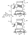
以下に本発明の実施の形態を説明する。図1は本発明に係る同時放電化装置の概略図であり、図2は図1における一方のプラズマ処理装置の部分拡大図である。
図1に示すように、誘導結合プラズマ処理装置A及びBは、それぞれベース1及び1′に載置される石英やアルミナセラミックス製の下部チャンバー2及び2′と、これらの下部チャンバー2及び2′の上に載置される石英やアルミナセラミックス製の上部チャンバー3及び3′と、更にこれらの上部チャンバー3及び3′の上にフランジを有する天板4及び4′を備えている。なお、天板4及び4′から反応ガスが導入されている。
【0012】
即ち、下部チャンバー2及び2′は、それぞれ上部チャンバー3及び3′と連通され、下部チャンバー2及び2′をそれぞれ被処理物W及びW′の処理領域とし、上部チャンバー3及び3′をそれぞれプラズマ発生領域としている。
【0013】
また、ベース1及び1′にはそれぞれ開口部5および5′が形成され、これらの開口部5及び5′の下方からそれぞれステージ6及び6′が臨んでいる。これらのステージ6及び6′はウェーハ等の被処理物W及びW′を載置して昇降動可能とされるとともにヒータが内蔵されている。さらに、開口部5及び5′の内周にそれぞれ排気リング7及び7′が設けられ、これらの排気リング7及び7′に形成した穴から排気を行うようにしている。なお、これらの排気リング7及び7′は発生したプラズマが飛ばないように絶縁処理を施すことが好ましい。
【0014】
また、それぞれの上部チャンバー3及び3′の外側に透磁率の高いアルミニウム合金製のファラディーシールド8及び8′が配置され、更にファラディーシールド8及び8′の外周にそれぞれコイル状電極9及び9′が3周巻回されている。
【0015】
一方、この実施の形態の特徴として、図1に示すように、高周波電源10が電力供給ライン11(即ち、電力供給ケーブル)で繋がれている。この高周波電源10の周波数は、400KHz〜27MHzである。
【0016】
また、この高周波電源10の一端はアースされ、他の端はM点で分岐されている。分岐された高周波電源10は、電力供給ライン11を通して、それぞれソリッドコンデンサー(即ち固定コンデンサー)12及び12′に繋がり、それらのソリッドコンデンサー12及び12′がさらにそれぞれコイル状電極9及び9′の上端に繋がっている。なお、コイル状電極9及び9′の下端は金属板13及び13′に繋がってからアースされている。
【0017】
そして、固定コンデンサー12及び12′のインピーダンスは一度決定するとその後は大きく変わらない。この実施例では、固定コンデンサー12及び12′のインピーダンスはそれぞれ同じ下流側におけるプラズマ発生用コイル状電極9および9′のインピーダンスの2.3〜2.7倍にしている。
【0018】
このように、高周波電源10から電力を同時にプラズマ処理装置A及びBに均等に流すためには、固定コンデンサー12及び12′が必要であるが、固定コンデンサー12及び12′のインピーダンスが不変であるので、プラズマが発生することにより見かけ上可変するプラズマ発生用コイル状電極9及び9′のインピーダンスの大小により電力の流れは偏在することになる。
【0019】
ところで、各プラズマ処理装置A及びBのインピーダンスは、各プラズマ処理装置側の固定コンデンサーとプラズマ発生用コイル状電極のインピーダンスの和とみなすことができるので、各固定コンデンサーのインピーダンスを各プラズマ発生用コイル状電極のインピーダンスよりも大きく設定すれば、各プラズマ発生用コイル状電極のインピーダンスの違いは、各プラズマ処理装置A及びB全体のインピーダンスから見た場合、それほど差がでない。しかし、各固定コンデンサーのインピーダンスが大きすぎても、また小さすぎても、安定して均等にプラズマ処理することができない。
【0020】
そこで鋭意研究したところ、前記固定コンデンサーのインピーダンスが同じ下流側における前記プラズマ発生用コイル状電極の2.3〜2.7倍とすることにより、プラズマ発生用コイル状電極のインピーダンスが多少可変しても同時に放電することができる。
【0021】
固定コンデンサーのインピーダンスがプラズマ発生用コイル状電極のインピーダンスの2.3倍未満の場合は、放電はどちらか一方でのみ生じ、同時放電は行われない。反対に固定コンデンサーのインピーダンスがプラズマ発生用コイル状電極のインピーダンスの約2.7倍以上ある場合は、コンデンサー自身の抵抗が大きくなりすぎてプラズマ効率が悪くなり、好ましくない。
【0022】
また、プラズマ処理装置A及びBは同時に放電することができるものの、各プラズマ処理装置A及びBに分配された電力は均一でなければ、アッシング又はエッチング等のレートに差が生じる。この実施例ではコンデンサー12及び12′同士の差異を設定値±5%以内(好ましくは2%)に設定する。即ち、固定コンデンサー同士の差異を小さくすることで、より均一に電力を分配することができる。
【0023】
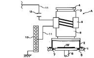
さらに、各プラズマ処理装置間の電力を均一するために、この実施例では、金属板13及び13′が微調整としてそれぞれコイル状電極9及び9′の下端のアース側に設置されている。それらの金属板の中、金属板13を拡大して図2に示す。金属板には奇数の穴が穿たれており、その中心の穴が最初の設定位置としている。複数のプラズマ処理装置のうちのどちらかのレートが低い方は、その金属板の穴を1つ伸ばす方向にずらす。逆の場合は縮む方向にずらす。このように、金属板の穴を1つずつずらすことによって、各プラズマ処理装置のレートをほぼ同じに調整することができる。
【0024】
以上において、高周波電源10からの電力が分岐点Mで分岐され、それぞれ固定コンデンサー12及び12′を通って、プラズマ処理装置A及びBに印加すると、コイル状電極9及び9′の軸方向電場がファラディーシールド8及び8′によって電気的に短絡され、その結果、上部チャンバー3及び3′内に容量結合型プラズマの発生が抑制され、主として誘導結合型プラズマが発生する。
【0025】
そして、発生した誘導結合型プラズマは天板4及び4′から導入された反応ガスとともにそれぞれ下部チャンバー2及び2′内に導入され、ステージ6及び6′上に載置されているウェーハ等の被処理物W及びW′に対してアッシングやエッチング等の所定の処理を行う。
【0026】
【発明の効果】
以上に説明したように、本発明によれば、高周波電源からの電力供給ラインが分岐部から各々の前記プラズマ処理装置に対して分岐されることで、RF電力を同時に各プラズマ処理装置に流すことができる。また、高周波電源の分岐部の下流側で各々の前記プラズマ処理装置との間にそれぞれ固定コンデンサーが設置されて、また例えば、前記固定コンデンサーのインピーダンスを前記プラズマ発生用コイル状電極の同じ下流側におけるインピーダンスの2.3〜2.7倍にすることで、一個の高周波電源から各プラズマ処理装置に同時に放電することができる。
【0027】
また、固定コンデンサー同士の差異を±5%以内に設定することで、各プラズマ処理装置のチャンバーに対してRF電力を均等に分配することができる。更に、プラズマ発生用コイル状電極は前記プラズマ処理装置に巻回し、且つ前記プラズマ発生用コイル状電極のアース電極側に微調整用の金属板を設置することで、より確実に各プラズマ処理装置を同時に放電させることができる。
即ち、一個の高周波電源で複数のプラズマ処理装置を同時に放電させ、各処理チャンバー内の被処理物に対して同時に且つ均一に処理を施すことができる。
【図面の簡単な説明】
【図1】本発明に係る同時放電化装置の概略図
【図2】図1に示すプラズマ処理装置の部分拡大図
【符号の説明】
A、B…プラズマ処理装置、 1、1′…ベース、 2、2′…下部チャンバー、 3、3′…上部チャンバー、 4、4′…天板、 5、5′…開口部、 6、6′…ステージ、 7、7′…排気リング、 8、8′…ファラディーシールド、 9、9′…プラズマ発生用コイル状電極、 10…高周波電源、 11…電力供給ライン、 12、12′…固定コンデンサー、 13、13′…金属板、 W、W′…被処理物。[0001]
TECHNICAL FIELD OF THE INVENTION
The present invention relates to a simultaneous discharge device for simultaneously discharging a plurality of plasma processing devices with one high-frequency power supply.
[0002]
[Prior art]
Conventional plasma processing apparatuses include a parallel plate type apparatus in which a pair of electrodes are arranged inside a chamber, and a plasma processing apparatus in which an antenna (electrode) for generating plasma is provided outside the chamber. Further, as the latter device, a pair of sheet-like electrodes are arranged facing each other on the outer periphery of the chamber, a high-frequency power source is connected to one of the pair of sheet-like electrodes, and the other is grounded. There is a type in which an annular coil-shaped electrode is arranged and a high-frequency power source is connected to the coil-shaped electrode.
[0003]
Plasma generated by applying a high frequency to a plasma processing apparatus using a high-frequency power supply includes a capacitively coupled plasma (CCP) and an inductively coupled plasma (ICP: Inductive Coupled Plasma). In a plasma processing apparatus using a sheet electrode, a capacitively coupled plasma is mainly generated, and in a plasma processing apparatus using a coiled electrode, an inductively coupled plasma is mainly generated.
[0004]
It has been found that inductively coupled plasma is preferred because capacitively coupled plasma damages the substrate being processed. In view of the above, a plasma processing apparatus using a coil-shaped electrode, as a prior art for further suppressing the generation of capacitively-coupled plasma, is disclosed in JP-A-5-502971, JP-A-8-50996 or JP-A-8-88220. Is disclosed in Japanese Patent Publication No. In each of these prior arts, a Faraday shield is disposed between an antenna (coil-shaped electrode) and a plasma processing chamber, and the axial electric field of the antenna is electrically short-circuited to suppress capacitively coupled plasma. Things.
[0005]
[Problems to be solved by the invention]
However, in the related art, there is no inconvenience when discharging one plasma processing apparatus using one high-frequency power supply, but when discharging a plurality of plasma processing apparatuses simultaneously with one high-frequency power supply, Since the arrangement state of the RF cable (that is, the power supply line) and the like constituting the coiled electrode is slightly different between the chambers in each plasma processing apparatus, the impedance is slightly different between the chambers. As a result, there is a problem that plasma is easily generated in a chamber having a low impedance, and it is difficult to generate plasma in a chamber having a high impedance.
[0006]
The present invention has been made in view of the above-described problem, and simultaneously discharges a plurality of plasma processing apparatuses with one high-frequency power supply, so that a film formed on a surface of an object to be processed such as a semiconductor wafer is identical in each chamber. It is an object of the present invention to provide a simultaneous discharge device capable of performing etching or ashing at a rate.
[0007]
[Means for Solving the Problems]
In order to solve the above problems, a simultaneous discharge device of the present invention is a simultaneous discharge device for simultaneously discharging a plurality of plasma processing devices with one high-frequency power supply, wherein the plurality of plasma processing devices have plasma generating electrodes. A plasma processing apparatus mainly including an inductively coupled plasma having a coil shape, wherein a power supply line from the high-frequency power supply is provided with a branch portion for each of the plasma processing devices and branched, and a downstream side of the branch portion. A fixed condenser was installed between each of the plasma processing apparatuses on the side. Here, it is preferable that the impedance of the fixed capacitor is 2.3 to 2.7 times the impedance of the coil electrode for plasma generation on the same downstream side.
[0008]
Since the power supply line from the high-frequency power supply is provided with a branch portion for each of the plasma processing apparatuses and is branched, RF power can be simultaneously supplied to each of the plasma processing apparatuses.
[0009]
A fixed capacitor is provided between each of the plasma processing apparatuses at a downstream side of the branch of the high-frequency power supply, and the impedance of the fixed capacitor is set to 2.3 of the impedance of the coil electrode for plasma generation. By increasing the power to 2.7 times, it is possible to simultaneously discharge from one high-frequency power supply to each plasma processing apparatus.
[0010]
Further, by setting the difference between the fixed capacitors within ± 5%, the RF power can be evenly distributed to the chambers of each plasma processing apparatus. Furthermore, by winding the coil-shaped electrode for plasma generation around the plasma processing apparatus, and installing a metal plate for fine adjustment on the earth electrode side of the coil-shaped electrode for plasma generation, each plasma processing apparatus can be more reliably used. It can be discharged at the same time.
That is, a plurality of plasma processing apparatuses can be simultaneously discharged by one high-frequency power supply, and the objects to be processed in each processing chamber can be simultaneously and uniformly processed.
[0011]
BEST MODE FOR CARRYING OUT THE INVENTION
Hereinafter, embodiments of the present invention will be described. FIG. 1 is a schematic view of a simultaneous discharge apparatus according to the present invention, and FIG. 2 is a partially enlarged view of one of the plasma processing apparatuses in FIG.
As shown in FIG. 1, the inductively coupled plasma processing apparatuses A and B include
[0012]
That is, the
[0013]
[0014]
Further, Faraday
[0015]
On the other hand, as a feature of this embodiment, as shown in FIG. 1, a high-
[0016]
One end of the high
[0017]
Once the impedances of the fixed
[0018]
As described above, the fixed
[0019]
By the way, the impedance of each plasma processing apparatus A and B can be regarded as the sum of the impedance of the fixed capacitor on each plasma processing apparatus side and the impedance of the coil electrode for plasma generation. If the impedance is set to be larger than the impedance of the shape electrodes, the difference between the impedances of the coil electrodes for plasma generation is not so different when viewed from the impedance of the entire plasma processing apparatuses A and B. However, if the impedance of each fixed capacitor is too large or too small, stable and uniform plasma processing cannot be performed.
[0020]
Therefore, as a result of intensive research, the impedance of the coil electrode for plasma generation was somewhat varied by setting the impedance of the fixed capacitor to 2.3 to 2.7 times that of the coil electrode for plasma generation on the same downstream side. Can also be discharged at the same time.
[0021]
When the impedance of the fixed capacitor is less than 2.3 times the impedance of the coil electrode for plasma generation, discharge occurs only in one of them, and simultaneous discharge is not performed. On the other hand, if the impedance of the fixed capacitor is about 2.7 times or more the impedance of the coil electrode for plasma generation, the resistance of the capacitor itself becomes too large and the plasma efficiency becomes poor, which is not preferable.
[0022]
Further, although the plasma processing apparatuses A and B can discharge at the same time, if the power distributed to each of the plasma processing apparatuses A and B is not uniform, a difference occurs in the rate of ashing or etching. In this embodiment, the difference between the
[0023]
Furthermore, in order to make the power between the plasma processing apparatuses uniform, in this embodiment, the
[0024]
In the above, when the electric power from the high
[0025]
Then, the generated inductively coupled plasma is introduced into the
[0026]
【The invention's effect】
As described above, according to the present invention, the power supply line from the high-frequency power supply is branched from the branch unit to each of the plasma processing apparatuses, so that the RF power is simultaneously supplied to each of the plasma processing apparatuses. Can be. In addition, fixed capacitors are respectively installed between the respective plasma processing apparatuses on the downstream side of the branch portion of the high-frequency power supply, and for example, the impedance of the fixed capacitors is set on the same downstream side of the plasma generating coil-shaped electrode. By setting the impedance to 2.3 to 2.7 times the impedance, a single high-frequency power supply can simultaneously discharge each plasma processing apparatus.
[0027]
Further, by setting the difference between the fixed capacitors within ± 5%, the RF power can be evenly distributed to the chambers of each plasma processing apparatus. Furthermore, the coil-shaped electrode for plasma generation is wound around the plasma processing apparatus, and a metal plate for fine adjustment is installed on the earth electrode side of the coil-shaped electrode for plasma generation, so that each of the plasma processing apparatuses can be more reliably used. It can be discharged at the same time.
That is, a plurality of plasma processing apparatuses can be simultaneously discharged by one high-frequency power supply, and the objects to be processed in each processing chamber can be simultaneously and uniformly processed.
[Brief description of the drawings]
1 is a schematic view of a simultaneous discharge apparatus according to the present invention; FIG. 2 is a partially enlarged view of a plasma processing apparatus shown in FIG. 1;
A, B: Plasma processing device, 1, 1 ': Base, 2, 2': Lower chamber, 3, 3 ': Upper chamber, 4, 4': Top plate, 5, 5 ': Opening, 6, 6 '... Stage, 7, 7' ... Exhaust ring, 8, 8 '... Faraday shield, 9,9' ... Coiled electrode for plasma generation, 10 ... High frequency power supply, 11 ... Power supply line, 12,12 '... Fixed Condenser, 13, 13 ': Metal plate, W, W': Workpiece.
Claims (4)
Priority Applications (4)
| Application Number | Priority Date | Filing Date | Title |
|---|---|---|---|
| JP2002168260A JP2004014904A (en) | 2002-06-10 | 2002-06-10 | Simultaneous discharging apparatus |
| US10/452,261 US6836073B2 (en) | 2002-06-10 | 2003-06-02 | Simultaneous discharge apparatus |
| TW092115077A TW200409567A (en) | 2002-06-10 | 2003-06-03 | Simultaneous discharging apparatus |
| KR10-2003-0035887A KR20030095256A (en) | 2002-06-10 | 2003-06-04 | Simultaneous discharge apparatus |
Applications Claiming Priority (1)
| Application Number | Priority Date | Filing Date | Title |
|---|---|---|---|
| JP2002168260A JP2004014904A (en) | 2002-06-10 | 2002-06-10 | Simultaneous discharging apparatus |
Publications (1)
| Publication Number | Publication Date |
|---|---|
| JP2004014904A true JP2004014904A (en) | 2004-01-15 |
Family
ID=29706802
Family Applications (1)
| Application Number | Title | Priority Date | Filing Date |
|---|---|---|---|
| JP2002168260A Pending JP2004014904A (en) | 2002-06-10 | 2002-06-10 | Simultaneous discharging apparatus |
Country Status (4)
| Country | Link |
|---|---|
| US (1) | US6836073B2 (en) |
| JP (1) | JP2004014904A (en) |
| KR (1) | KR20030095256A (en) |
| TW (1) | TW200409567A (en) |
Families Citing this family (13)
| Publication number | Priority date | Publication date | Assignee | Title |
|---|---|---|---|---|
| KR100720989B1 (en) * | 2005-07-15 | 2007-05-28 | 주식회사 뉴파워 프라즈마 | Multi chamber plasma process system |
| CA2516499A1 (en) * | 2005-08-19 | 2007-02-19 | Atlantic Hydrogen Inc. | Decomposition of natural gas or methane using cold arc discharge |
| US20080289494A1 (en) * | 2005-08-19 | 2008-11-27 | Atlantic Hydrogen Inc. | Decomposition of natural gas or methane using cold arc discharge |
| US7453191B1 (en) * | 2007-07-06 | 2008-11-18 | Uion Co., Ltd. | Induction concentration remote atmospheric pressure plasma generating apparatus |
| US9111729B2 (en) * | 2009-12-03 | 2015-08-18 | Lam Research Corporation | Small plasma chamber systems and methods |
| US9190289B2 (en) * | 2010-02-26 | 2015-11-17 | Lam Research Corporation | System, method and apparatus for plasma etch having independent control of ion generation and dissociation of process gas |
| US8999104B2 (en) | 2010-08-06 | 2015-04-07 | Lam Research Corporation | Systems, methods and apparatus for separate plasma source control |
| US9155181B2 (en) | 2010-08-06 | 2015-10-06 | Lam Research Corporation | Distributed multi-zone plasma source systems, methods and apparatus |
| US9449793B2 (en) | 2010-08-06 | 2016-09-20 | Lam Research Corporation | Systems, methods and apparatus for choked flow element extraction |
| US9967965B2 (en) | 2010-08-06 | 2018-05-08 | Lam Research Corporation | Distributed, concentric multi-zone plasma source systems, methods and apparatus |
| US9177762B2 (en) | 2011-11-16 | 2015-11-03 | Lam Research Corporation | System, method and apparatus of a wedge-shaped parallel plate plasma reactor for substrate processing |
| US10283325B2 (en) | 2012-10-10 | 2019-05-07 | Lam Research Corporation | Distributed multi-zone plasma source systems, methods and apparatus |
| JP5960758B2 (en) * | 2014-07-24 | 2016-08-02 | 東京エレクトロン株式会社 | Substrate processing system and substrate processing apparatus |
Family Cites Families (6)
| Publication number | Priority date | Publication date | Assignee | Title |
|---|---|---|---|---|
| US4887005A (en) * | 1987-09-15 | 1989-12-12 | Rough J Kirkwood H | Multiple electrode plasma reactor power distribution system |
| DE69128345T2 (en) | 1990-01-04 | 1998-03-26 | Mattson Tech Inc | INDUCTIVE PLASMA REACTOR IN THE LOWER HIGH FREQUENCY RANGE |
| US5540800A (en) | 1994-06-23 | 1996-07-30 | Applied Materials, Inc. | Inductively coupled high density plasma reactor for plasma assisted materials processing |
| JPH0850996A (en) | 1994-08-05 | 1996-02-20 | Aneruba Kk | Plasma treatment device |
| JP3279919B2 (en) | 1996-05-14 | 2002-04-30 | 東京応化工業株式会社 | Simultaneous discharge device |
| JP3868217B2 (en) * | 2001-02-09 | 2007-01-17 | 東京応化工業株式会社 | Plasma processing equipment |
-
2002
- 2002-06-10 JP JP2002168260A patent/JP2004014904A/en active Pending
-
2003
- 2003-06-02 US US10/452,261 patent/US6836073B2/en not_active Expired - Fee Related
- 2003-06-03 TW TW092115077A patent/TW200409567A/en not_active IP Right Cessation
- 2003-06-04 KR KR10-2003-0035887A patent/KR20030095256A/en not_active Application Discontinuation
Also Published As
| Publication number | Publication date |
|---|---|
| KR20030095256A (en) | 2003-12-18 |
| TW200409567A (en) | 2004-06-01 |
| US20030227259A1 (en) | 2003-12-11 |
| TWI325288B (en) | 2010-05-21 |
| US6836073B2 (en) | 2004-12-28 |
Similar Documents
| Publication | Publication Date | Title |
|---|---|---|
| JP3653524B2 (en) | Plasma generation method and plasma generation apparatus including inductively coupled plasma generation source | |
| TWI435664B (en) | Hybrid rf capacitively and inductively coupled plasma source using multifrequency rf powers and methods of use thereof | |
| JP4057547B2 (en) | ICP antenna and plasma generator using the same | |
| US5874704A (en) | Low inductance large area coil for an inductively coupled plasma source | |
| KR20000053680A (en) | Antenna device for generating inductively coupled plasma | |
| TW201448032A (en) | Plasma processing device | |
| JP2006221852A (en) | Induction coupled plasma generator | |
| JP2000323298A (en) | Plasma treatment device and method | |
| JP2004014904A (en) | Simultaneous discharging apparatus | |
| TWI279169B (en) | Plasma processing apparatus capable of performing uniform plasma treatment by preventing drift in plasma discharge current | |
| TW201911977A (en) | Upper electrode element, reaction chamber and semiconductor processing device | |
| JP2006286536A (en) | Plasma generation method, induction coupling type plasma source, and plasma treatment device | |
| JPH0850996A (en) | Plasma treatment device | |
| JP2972707B1 (en) | Plasma etching apparatus and plasma etching method | |
| KR20100061126A (en) | Compound plasma reactor | |
| JP6530859B2 (en) | Plasma processing system | |
| WO2008031321A1 (en) | Inductive coupling coil and inductive coupling plasma apparatus thereof | |
| KR101214361B1 (en) | Plasma generation apparatus | |
| US20200219698A1 (en) | Recursive coils for inductively coupled plasmas | |
| TW469533B (en) | Dry etching apparatus | |
| JP3460113B2 (en) | Plasma processing equipment | |
| KR100743842B1 (en) | Plasma reactor having plasma chamber coupled with magnetic flux channel | |
| JPH1022265A (en) | Plasma generating device | |
| JP3485013B2 (en) | Plasma processing method and apparatus | |
| JP2001052895A (en) | Plasma generating device and plasma processing device equipped therewith |
Legal Events
| Date | Code | Title | Description |
|---|---|---|---|
| A621 | Written request for application examination |
Free format text: JAPANESE INTERMEDIATE CODE: A621 Effective date: 20040622 |
|
| A977 | Report on retrieval |
Free format text: JAPANESE INTERMEDIATE CODE: A971007 Effective date: 20050111 |
|
| A131 | Notification of reasons for refusal |
Free format text: JAPANESE INTERMEDIATE CODE: A131 Effective date: 20060822 |
|
| A521 | Written amendment |
Free format text: JAPANESE INTERMEDIATE CODE: A523 Effective date: 20061023 |
|
| A131 | Notification of reasons for refusal |
Free format text: JAPANESE INTERMEDIATE CODE: A131 Effective date: 20070320 |
|
| A02 | Decision of refusal |
Free format text: JAPANESE INTERMEDIATE CODE: A02 Effective date: 20070710 |