JP6530859B2 - Plasma processing system - Google Patents
Plasma processing system Download PDFInfo
- Publication number
- JP6530859B2 JP6530859B2 JP2018511164A JP2018511164A JP6530859B2 JP 6530859 B2 JP6530859 B2 JP 6530859B2 JP 2018511164 A JP2018511164 A JP 2018511164A JP 2018511164 A JP2018511164 A JP 2018511164A JP 6530859 B2 JP6530859 B2 JP 6530859B2
- Authority
- JP
- Japan
- Prior art keywords
- high frequency
- plasma
- sample
- electrode
- processing apparatus
- Prior art date
- Legal status (The legal status is an assumption and is not a legal conclusion. Google has not performed a legal analysis and makes no representation as to the accuracy of the status listed.)
- Active
Links
Images


Classifications
-
- H—ELECTRICITY
- H01—ELECTRIC ELEMENTS
- H01J—ELECTRIC DISCHARGE TUBES OR DISCHARGE LAMPS
- H01J37/00—Discharge tubes with provision for introducing objects or material to be exposed to the discharge, e.g. for the purpose of examination or processing thereof
- H01J37/32—Gas-filled discharge tubes
- H01J37/32431—Constructional details of the reactor
- H01J37/32697—Electrostatic control
- H01J37/32706—Polarising the substrate
-
- H—ELECTRICITY
- H01—ELECTRIC ELEMENTS
- H01J—ELECTRIC DISCHARGE TUBES OR DISCHARGE LAMPS
- H01J37/00—Discharge tubes with provision for introducing objects or material to be exposed to the discharge, e.g. for the purpose of examination or processing thereof
- H01J37/32—Gas-filled discharge tubes
- H01J37/32431—Constructional details of the reactor
- H01J37/32532—Electrodes
-
- H—ELECTRICITY
- H01—ELECTRIC ELEMENTS
- H01J—ELECTRIC DISCHARGE TUBES OR DISCHARGE LAMPS
- H01J37/00—Discharge tubes with provision for introducing objects or material to be exposed to the discharge, e.g. for the purpose of examination or processing thereof
- H01J37/32—Gas-filled discharge tubes
- H01J37/32009—Arrangements for generation of plasma specially adapted for examination or treatment of objects, e.g. plasma sources
- H01J37/32082—Radio frequency generated discharge
- H01J37/321—Radio frequency generated discharge the radio frequency energy being inductively coupled to the plasma
-
- H—ELECTRICITY
- H01—ELECTRIC ELEMENTS
- H01J—ELECTRIC DISCHARGE TUBES OR DISCHARGE LAMPS
- H01J37/00—Discharge tubes with provision for introducing objects or material to be exposed to the discharge, e.g. for the purpose of examination or processing thereof
- H01J37/32—Gas-filled discharge tubes
- H01J37/32009—Arrangements for generation of plasma specially adapted for examination or treatment of objects, e.g. plasma sources
- H01J37/32082—Radio frequency generated discharge
- H01J37/32174—Circuits specially adapted for controlling the RF discharge
-
- H—ELECTRICITY
- H01—ELECTRIC ELEMENTS
- H01J—ELECTRIC DISCHARGE TUBES OR DISCHARGE LAMPS
- H01J37/00—Discharge tubes with provision for introducing objects or material to be exposed to the discharge, e.g. for the purpose of examination or processing thereof
- H01J37/32—Gas-filled discharge tubes
- H01J37/32431—Constructional details of the reactor
- H01J37/32532—Electrodes
- H01J37/32541—Shape
-
- H—ELECTRICITY
- H01—ELECTRIC ELEMENTS
- H01J—ELECTRIC DISCHARGE TUBES OR DISCHARGE LAMPS
- H01J37/00—Discharge tubes with provision for introducing objects or material to be exposed to the discharge, e.g. for the purpose of examination or processing thereof
- H01J37/32—Gas-filled discharge tubes
- H01J37/32431—Constructional details of the reactor
- H01J37/32715—Workpiece holder
-
- H—ELECTRICITY
- H01—ELECTRIC ELEMENTS
- H01J—ELECTRIC DISCHARGE TUBES OR DISCHARGE LAMPS
- H01J2237/00—Discharge tubes exposing object to beam, e.g. for analysis treatment, etching, imaging
- H01J2237/32—Processing objects by plasma generation
- H01J2237/33—Processing objects by plasma generation characterised by the type of processing
- H01J2237/334—Etching
Description
本発明は、真空容器内部の処理室内に配置された半導体ウエハ等の板状の試料を処理室内に形成したプラズマを用いて処理するプラズマ処理装置に係り、特に、処理室内に配置された試料台内に配置した電極に電力を供給して試料台上面上に試料を静電吸着して保持しつつ当該試料を処理するプラズマ処理装置に関する。 The present invention relates to a plasma processing apparatus for processing a plate-like sample such as a semiconductor wafer or the like disposed in a processing chamber inside a vacuum vessel using plasma formed in the processing chamber, and in particular, a sample stage disposed inside the processing chamber The present invention relates to a plasma processing apparatus for processing a sample while supplying electric power to an electrode disposed in the electrode to electrostatically hold and hold the sample on the upper surface of the sample stage.
真空容器等の処理容器内部の処理室に配置した半導体ウエハ等の試料をプラズマを用いてエッチングするドライエッチングに代表されるプラズマ処理は、通常、減圧された処理室内に処理用のガスを導入し、処理室内に電界または磁界を供給して当該ガスの原子または分子を励起してプラズマを形成し、このプラズマを用いて試料を処理する技術である。この技術においては、処理室内で形成されたプラズマを試料の表面に曝し、この表面に予め形成されたマスク層を含む複数の膜層を備えた膜構造のマスク部以外の処理対象の膜層をエッチングすることで所望の形状が得られる。 In plasma processing represented by dry etching in which a sample such as a semiconductor wafer disposed in a processing chamber inside a processing chamber such as a vacuum container is etched using plasma, a processing gas is usually introduced into the processing chamber under reduced pressure. An electric field or a magnetic field is supplied into a processing chamber to excite atoms or molecules of the gas to form a plasma, and the plasma is used to process a sample. In this technique, the plasma formed in the processing chamber is exposed to the surface of the sample, and the film layer to be treated other than the mask portion of the film structure provided with a plurality of film layers including the mask layer formed in advance on this surface The desired shape can be obtained by etching.
このようなプラズマが内側で生成され試料が処理される真空容器を含むプラズマ処理装置において、プラズマを形成する技術として、誘導電界によるもの、平行に配置された平板状の電極間の空間の電界によるもの(電極間の電界としてマグネトロンによるもの含む)や所定の空間に放射された電界の波動によるもの(μ波の電界と磁界とによる電子サイクロトロン共鳴を用いるものを含む)が主に用いられている。なお、現在では、誘導結合による方式におけるプラズマの生成に13.56MHzの高周波の電界が用いられるものが一般的である。 In a plasma processing apparatus including a vacuum vessel in which such plasma is generated inside and a sample is processed, as a technique for forming a plasma, by an induction electric field, by an electric field of a space between parallel plate-like electrodes Mainly used are those (including those by a magnetron as the electric field between the electrodes) and those by the waves of the electric field radiated to a predetermined space (including those using electron cyclotron resonance by μ electric and magnetic fields) . At present, it is common to use a 13.56 MHz high frequency electric field to generate plasma in the inductive coupling method.
また、電子サイクロトロン共鳴(ELectron Cyclotron Resonace:ECR)による方式では、例えば、2.45GHzのより高い周波数の電界が用いられる。これら誘導結合および電子サイクロトロン共鳴によりプラズマを形成するプラズマ処理装置では、通常、プラズマの生成とは別に、試料にイオンを誘引する電位を形成して試料台上に載せられて保持される試料の表面へプラズマ中のイオンを入射させてプラズマと電位を形成する電力とを結合させる。 In addition, in the method based on EL cyclotron resonance (ECR), for example, a higher frequency electric field of 2.45 GHz is used. In the plasma processing apparatus which forms a plasma by these inductive coupling and electron cyclotron resonance, the surface of the sample which is usually placed on the sample table and held by forming an electric potential for attracting ions to the sample separately from the generation of the plasma. The ions in the plasma are introduced to couple the power of the plasma and the potential to form a potential.
このような電力の供給により形成された電位に誘引された電荷を有したイオンが試料表面と衝突する際のエネルギーを利用してこの試料表面に予め形成されて配置された処理対象の膜のエッチングを当該衝突の方向に促進することが一般的に行われている。このようなイオンのエネルギーの大きさやイオンの入射の方向を制御して所望の形状が得られるエッチング処理を実現するため、上記プラズマを形成するために供給されるものとは異なる(一般的にはより低い)周波数の高周波電力が試料をプラズマに対して対面させて支持する試料台の内部に配置された電極へその大きさが調節されつつ供給される。 Etching of a film to be processed which is formed in advance and disposed on the surface of the sample by utilizing energy when ions having charges induced to the potential formed by the supply of power collide with the surface of the sample It is common practice to promote in the direction of the collision. In order to realize an etching process in which a desired shape is obtained by controlling the magnitude of energy of such ions and the direction of incidence of ions, it is different from that supplied to form the plasma (generally, The lower frequency radio frequency power is supplied to the electrode arranged inside the sample stage supporting the sample facing the plasma with its size being adjusted.
一方、平行平板によるプラズマを用いたプラズマ処理装置では、従来から、13.56MHzの高周波の電界が平板間でのプラズマの生成に用いられてきたが、近年はVHF帯(例えば、30MHz乃至300MHz)の電界が用いられるようになっている。このようなプラズマを生成するために供給される電界の周波数にVHF帯が用いられるようになった理由は、プラズマの密度の向上と処理室内の圧力が相対的に低い条件においても処理室内に安定して放電を形成してプラズマを生成できるようにするためである。 On the other hand, in a plasma processing apparatus using parallel plate plasma, a 13.56 MHz high frequency electric field has conventionally been used to generate plasma between plates, but in recent years the VHF band (eg, 30 MHz to 300 MHz) Electric field is used. The reason why the VHF band has come to be used for the frequency of the electric field supplied to generate such plasma is that the plasma density is improved and the inside of the processing chamber is stable even under relatively low pressure conditions. To form a discharge and to generate a plasma.
また、このような平行平板を用いたプラズマ処理装置においても、先の誘導電界によるものやECR等のより高い周波数の電界の波動によるものと同様に、プラズマを生成するためのものとは別に、一方の平板状の電極である試料が載置される試料台の内部に配置された電極に供給する高周波電力の大きさを調節してプラズマから試料の表面に入射するイオンのエネルギーを調節する技術も用いられるようになってきている。 Also, in the plasma processing apparatus using such a parallel plate, apart from the one for generating plasma, as in the case of the above-mentioned induced electric field or the wave of a higher frequency electric field such as ECR, Technology for adjusting the energy of ions incident on the surface of the sample from the plasma by adjusting the magnitude of the high frequency power supplied to the electrode disposed inside the sample stage on which the sample, which is one flat plate-like electrode, is placed Is also being used.
このような試料上面上方にプラズマとの間で形成されるバイアス電位の分布を調節するために試料台内の電極に供給される高周波の電力は、現在は、例えば、数百kHzから数MHzの周波数のものが用いられている。このような入射するイオンのエネルギーの調節に用いる高周波の電力も、従来のものより高いMHz帯またはそれ以上の周波数帯のものが用いられる傾向にある。 The high frequency power supplied to the electrode in the sample stage to adjust the distribution of the bias potential formed between the upper surface of the sample and the plasma is, for example, several hundred kHz to several MHz at present. The frequency is used. The high frequency power used to adjust the energy of such incident ions also tends to be used in a frequency band higher than that of the conventional one in the MHz band or higher.
なお、このようなプラズマ処理装置では、処理中に試料の温度を処理に適した範囲内の値に制御するために、試料台の内部にその内側を冷媒が循環して通流する冷媒流路を備えて試料台の温度が調節される。さらに、試料が載せられ静電吸着された試料台上面と試料との間の隙間にHeガス等の熱伝達性を有する流体が供給され、試料台(または冷媒流路内の冷媒)と試料との間での熱伝達を促進させている。 In such a plasma processing apparatus, in order to control the temperature of the sample to a value within the range suitable for the processing during processing, a refrigerant flow path through which the refrigerant circulates and flows inside the sample stage. The temperature of the sample table is adjusted. Further, a fluid having heat conductivity such as He gas is supplied to the gap between the sample and the sample table on which the sample is mounted and electrostatically adsorbed, and the sample table (or the refrigerant in the coolant channel) and the sample Promote heat transfer between
また、冷媒による温度の調節に加えて、試料台上部の内部に配置されたヒータを用いて試料を加熱することも行われている。上記のような技術の例としては、特開2014−056706号公報(特許文献1)に開示されたものが従来知られていた。本特許文献1には、金属製の円筒型チャンバの内部に配置されて半導体ウエハWが載置されるサセプタと、このサセプタと各々がマッチングユニットを介して電気的に接続された2つの高周波電源と、サセプタの上方でこれと平行に向かい合って配置されチャンバの天井を構成する上部電極を兼ねたシャワーヘッドと、サセプタ内部に配置された冷媒通路および静電チャック並びにヒータとを備えたプラズマエッチング装置が開示されている。
Moreover, in addition to the control of the temperature by a refrigerant | coolant, heating a sample using the heater arrange | positioned inside the upper part of a sample stand is also performed. As an example of the above-mentioned technique, what was indicated by JP, 2014-056706, A (patent documents 1) was conventionally known. In
さらに、本特許文献1が開示するプラズマ処理装置は、サセプタにはプラズマ形成用の27MHz以上の周波数の高周波電力とイオン引き込みに適した13MHz以下の低い周波数の高周波電力とが供給されて、接地電位にされた上部電極との間の処理室の空間に容量結合型のプラズマを生成する陰極結合型のものである。さらに、本従来技術では、サセプタ内の内側(中心部)と外側(周辺部)の領域の各々に配置されたヒータである発熱線と各々のヒータ用の電源とがヒータ回路用フィルタを介して接続され、ヒータ回路用のフィルタは、プラズマの生成やウエハWに印加される2つの周波数の高周波電力のノイズがヒータ給電回路へ流入することを遮断して抑制しているため、ヒータを用いたウエハWの温度の制御の正確性やプラズマの生成および高周波電力によるバイアス電位の安定性や再現性が向上する。
Furthermore, in the plasma processing apparatus disclosed in
上記の従来技術は、次の点について考慮が不十分であったために問題が生じていた。 The above-mentioned prior art has a problem because the following points are not sufficiently considered.
すなわち、上記のプラズマの生成と当該プラズマによる試料の処理中に試料へのイオンの入射エネルギーの各々を異なる高周波電源からの電力を用いて調節する従来の技術において、試料を支持する試料台内部に配置されたヒータや試料の静電吸着用の電極に接続された給電経路を構成するケーブルやその上の回路のインピーダンスの大きさは、プラズマを形成するための高周波電力やバイアス電位形成用の高周波電力がこれら経路や回路に流入することやこれによる悪影響を抑制して所望の処理の結果が得られるような範囲内の適切な値を有している必要がある。このため、一般的に、給電経路を構成するケーブルや給電経路上に配置される回路を構成する各素子や部品は、通常は、それらのインピーダンスが予め設計の際に定められた値を有したものとして当該給電経路上に取り付けられ配置される。 That is, in the prior art in which each of the above-mentioned plasma generation and the incident energy of ions to the sample during processing of the sample by the plasma is adjusted using power from different high frequency power sources, The size of the impedance of the circuit that forms the feed path connected to the heater or the electrode for electrostatic adsorption of the sample and the circuit on it is the high frequency power for forming plasma and the high frequency for forming bias potential. It is necessary to have an appropriate value within the range in which the power flows into these paths and circuits and the adverse effect thereof is suppressed to obtain the desired processing result. For this reason, in general, the cables constituting the feeding path and the respective elements and parts constituting the circuit disposed on the feeding path usually have their impedance values determined in advance in the design. It is attached and arranged on the said feed route as a thing.
しかしながら、バイアス形成用の電力の大きさが大きくなったり、或いはプラズマの生成にVHF帯以上の周波数の高周波を用いた場合には、上記ヒータ等の電極及びこれに接続された給電経路や回路を構成する素子の静電容量やインダクタンス等回路定数のばらつきや変化がわずかに生じても、これらの経路や回路に漏洩する高周波電力の大きさが変動してしまう。このようなばらつきは、ケーブルの長さや形状、各素子に固有の性能や特性の差によって生じる。このため、試料表面に形成されるバイアス電位、或いは試料上面上方のプラズマの密度の大きさや分布といったプラズマの生成される状態、曳いては試料の処理結果としての試料表面の処理後の形状のばらつき等処理の再現性に影響を及ぼすことが判明してきた。 However, when the size of the power for bias formation is increased or when high frequency of frequency higher than VHF band is used for generation of plasma, the electrode such as the heater and the feeding path and circuit connected thereto are used. Even if slight variations or changes in circuit constants such as capacitance and inductance of the elements to be configured occur, the magnitude of the high frequency power leaked to these paths and circuits will vary. Such variations are caused by differences in cable length and shape, and performance and characteristics unique to each element. Therefore, the state of plasma generation, such as the bias potential formed on the sample surface or the size and distribution of the density of plasma above the upper surface of the sample, that is, the variation in the shape of the sample surface as a result of processing the sample It has been found to affect the repeatability of isoprocessing.
また、このようなバラツキは同じ構成を備えた複数の装置同士の間において生起して装置間差を大きくしてしまうという問題が有った。さらに、経路や回路に流入する高周波電力の変化によって、静電吸着の機能や加熱による試料の温度調節の精度が損なわれ処理の歩留まりが損なわれてしまう問題が生じるという点について、上記従来技術では考慮されていなかった。 In addition, there is a problem that such variations occur among a plurality of devices having the same configuration, and the difference between the devices is increased. Furthermore, with respect to the point that the problem of the function of electrostatic adsorption and the accuracy of temperature control of the sample due to heating being impaired and the yield of processing being impaired is caused by the change of the high frequency power flowing into the path and circuit. It was not considered.
本発明の目的は、このような問題を考慮して、歩留まりを向上させたプラズマ処理装置を提供することにある。 An object of the present invention is to provide a plasma processing apparatus with improved yield in consideration of such problems.
上記目的は、真空容器内部に配置されその内側でプラズマが形成される処理室と、この処理室内に配置され前記プラズマを用いて処理される試料がその上に載せられる試料台と、この試料台上面を構成してその上に前記試料が載せられる誘電体製の膜内に配置され当該試料を吸着するための電力が供給されて異なる極性が形成される膜状の2つの電極と、当該2つの電極と各々の電源との間の給電路上に配置され前記2つの電極各々に接続された2つの給電線路が同じ軸回りに並列に巻かれたコイル状部分と、このコイル状部分と前記2つ電極との間において前記2つの給電線路を接続しコンデンサを備えたバイパス線路とを備えたプラズマ処理装置により達成される。 The above object is to provide a processing chamber which is disposed inside a vacuum vessel and in which a plasma is formed, a sample stage which is disposed in the processing chamber and on which a sample to be treated using the plasma is placed. Two film-like electrodes disposed in a dielectric film on which an upper surface is to be placed and on which the sample is placed and power for adsorbing the sample is supplied and different polarities are formed; A coiled portion in which two feed lines disposed on feed paths between two electrodes and each power source and connected to each of the two electrodes are wound in parallel around the same axis; This is achieved by a plasma processing apparatus comprising: a bypass line connected to the two feed lines between the two electrodes and including a capacitor.
本発明により、特に周波数が高いプラズマ生成用の高周波電力が双極型の静電吸着電極の回路へ流入したりその機差を抑制でき、プラズマ生成の変動および再現性の低下や装置間差の発生を抑制することが可能となり、歩留まりを向上させたプラズマ処理装置を提供することができる。 According to the present invention, the high frequency power for plasma generation particularly at high frequency can flow into the circuit of the bipolar electrostatic adsorption electrode and the machine difference thereof can be suppressed, and the fluctuation of plasma generation and the reduction of reproducibility and the generation of the difference between devices Can be suppressed, and a plasma processing apparatus with an improved yield can be provided.
本発明の実施例を図面を用いて以下説明する。 Embodiments of the present invention will be described below with reference to the drawings.
本発明の実施例を図1乃至7を用いて説明する。 Embodiments of the present invention will be described with reference to FIGS.
まず、図1を用いて本実施例の構成の概要を説明する。図1は、本発明の実施例に係るプラズマ処理装置の構成の概略を模式的に示す縦断面図である。 First, the outline of the configuration of the present embodiment will be described with reference to FIG. FIG. 1 is a longitudinal sectional view schematically showing the outline of the configuration of a plasma processing apparatus according to an embodiment of the present invention.
図1に示すプラズマ処理装置は、側壁が円筒形を有した真空容器10とその外周を囲み及び上面を覆って配置された電磁コイル1、真空容器10下方でその下部と接続された管路である排気口27及びこれと連結されて真空容器10下方に配置されたターボ分子ポンプ等の真空ポンプ(図示せず)を備えている。さらに、真空容器10の内部には、処理対象の試料3が配置されてプラズマが形成される空間である処理室40が配置されている。
The plasma processing apparatus shown in FIG. 1 includes a
本実施例のプラズマ処理装置では、処理室40には試料3がその上面に載せられてこれを支持する試料台2が配置されている。さらに、試料台2の上方であって真空容器10の円筒形の内側側壁に周囲を囲まれた空間の上下方の箇所には、真空容器10内部に配置された円板状の上部電極4と試料台2の内部に配置された円板形状を有した金属製の下部電極2’とが各々対向して備えられている。
In the plasma processing apparatus of the present embodiment, a sample table 2 is mounted on the upper surface of the
即ち、円筒形を有した空間である処理室40上方には、半導体ウエハ等の円形またはこれと同等な形状を有した基板状の試料3がその上面上に載置される試料台2の当該上面上方でこれに対向して配置され円板形状を有した上部電極4が配置されている。さらに、当該上部電極4下面下方の試料3の側には当該下面を覆って隙間を開けて配置されたシャワープレート5が配置されている。
That is, above the
上部電極4とシャワープレート5との間に配置された隙間は、ガス導入ライン6の一端部と連結されこれを構成する配管内部と隙間とが連通されて配置される。ガス導入ライン6の配管の他端側には、図示していないが、内部に処理室40より高圧にされたガスが貯留された容器を備えたガス源及びこのガス源と他端部との間の配管上に配置されて配管内をガス源から隙間に向けて流れるガスの流量を増減して調節するマスフローコントローラ(MFC)が配置されている。
A gap disposed between the upper electrode 4 and the shower plate 5 is connected to one end of the gas introduction line 6 so that the inside of the pipe constituting this and the gap communicate with each other. Although not shown in the drawing, the other end of the piping of the gas introduction line 6 has a gas source including a container in which a gas which is at a higher pressure than the
この構成により、ガス源の貯留部から配管を通ってMFCにより流量が調節されたガスが、上部電極4とシャワープレート5との間の隙間に導入されて当該隙間内を拡散して充満する。その後、ガスはシャワープレート5の中央部に配置された複数の貫通孔であるガス導入孔を通って試料台2の上方から下方に向けて処理室40に導入される。
With this configuration, the gas whose flow rate is adjusted by the MFC from the reservoir of the gas source is introduced into the gap between the upper electrode 4 and the shower plate 5 to diffuse and fill the gap. Thereafter, the gas is introduced into the
本実施例において、上部電極4は導電性材料であるアルミまたはステンレス等で形成されている。その内部には通路が配置されその内部にチラー等の温度調節器を含む上部電極温度制御手段7において所定の範囲内の温度にされた冷媒が循環して供給される。このことにより、上部電極4の温度は、試料3の処理中にその処理に適した範囲内の値になるように調節される。
In the present embodiment, the upper electrode 4 is formed of a conductive material such as aluminum or stainless steel. A passage is disposed in the interior thereof, and a refrigerant whose temperature is within a predetermined range is circulated and supplied in the upper electrode temperature control means 7 including a temperature controller such as a chiller therein. As a result, the temperature of the upper electrode 4 is adjusted during processing of the
本実施例のシャワープレート5は、石英やシリコン等の誘電体材料から構成された円板形状を有した部材である。シャワープレート5は、処理室40の天井面の中央部を構成して、処理室40下部において円筒形を有した試料台2の上面またはこれに載せられた円板形状を有した試料3と対向して、その中心軸を試料台2、試料3の載置面または処理室40の上下方向の中心軸と位置を合致またはこれと見做せる程度に近似した同等の位置に配置されている。さらに、シャワープレート5の外周側であって真空容器10の内周壁面との間には、シャワープレート5の外周を囲んで石英等の誘電体材料から構成され上部電極4またはシャワープレート5を真空容器10から絶縁するためのリング状の部材である、絶縁リング13が配置されている。
The shower plate 5 of the present embodiment is a member having a disk shape made of a dielectric material such as quartz or silicon. The shower plate 5 constitutes the central portion of the ceiling surface of the
本実施例の上部電極4、下部電極2’各々は、真空容器10の外部に配置され異なる周波数の電力を出力する各々の高周波電源と電気的に接続されている。本実施例では、試料3の処理中には、各々の高周波電源から出力された高周波電力が上部電極4及び下部電極2’に供給されると共に、電磁コイル1で磁場が生起され、処理室内40に電界と磁界とが並行して供給される。
Each of the upper electrode 4 and the lower electrode 2 'of the present embodiment is electrically connected to each high frequency power source which is disposed outside the
すなわち、上部電極4は放電用高周波電源8と同軸ケーブル等の給電経路を通して電気的に接続され、放電用高周波電力整合器9を介して所定の周波数の高周波電力が供給される。本実施例では、放電用高周波電力として200MHzの高周波帯の周波数が用いられる。また、真空容器10の蓋を構成する上部の内部に配置される上部電極4は、その上方および周囲が石英、テフロン(登録商標)および空間等で形成される上部電極絶縁体12により囲まれて内蔵され、上部電極4が真空容器10から電気的に絶縁される。
That is, the upper electrode 4 is electrically connected to the discharge high frequency power supply 8 through a feed path such as a coaxial cable, and high frequency power of a predetermined frequency is supplied via the discharge high frequency power matching unit 9. In the present embodiment, a frequency in the high frequency band of 200 MHz is used as the high frequency power for discharge. Further, the upper electrode 4 disposed inside the upper portion constituting the lid of the
試料台2内部の下部電極2’は、試料台2に載せられた試料3上面上方にバイアス電位を形成するための所定の周波数(本実施例では4MHz)の高周波電力を出力するバイアス用高周波電源20と同軸ケーブル等の給電経路29を通して電気的に接続されている。試料3の処理中に、バイアス用高周波電源20からバイアス用高周波電力整合器21を介してバイアス用の4MHzの高周波電力が下部電極2’に供給される。
The lower electrode 2 'inside the sample table 2 outputs a high frequency power of a predetermined frequency (4 MHz in this embodiment) for forming a bias potential above the upper surface of the
試料3が試料台2上面に載せられて保持され、処理室40が真空容器10の側壁外側に対して密封された状態で、処理室40の上部電極4及び下部電極2’の間の円筒形の空間には、MFCによりその供給される流量または速度が調節されつつシャワープレート5のガス導入孔からガスが導入されると共に、試料台2下方の処理室40の底面に配置された排気用の開口と連通された排気口27から処理室40内のガスの原子、分子等の粒子が、排気口27内に配置されてその流路断面積を当該流路を横切る軸回りに板状のフラップを回転させて増減する排気調節バルブ26によって排気の流量または速度を調節されつつ排気される。この状態で、図示されない制御装置からの指令信号に基いてMFC及び排気調節バルブ26の動作が調節され、上記処理室40へのガスの供給と排気との流量または速度のバランスにより、処理室40内の圧力がプラズマ11の放電とその維持あるいは試料3の処理に適した範囲内の値にされる。
The cylindrical shape between the upper electrode 4 and the
この状態で、上記ガスの原子または分子を解離あるいは電離させて放電を生起可能にその出力が調節されて供給された高周波電力によって形成された電界及び電磁コイル1による磁界が供給され、これら電界および磁界とによるECRが生起されて処理室40内にプラズマ11が形成される。このように、本実施例のプラズマ処理装置は、電界とともに磁界を供給する(有磁場の)平行平板型のプラズマ処理装置である。
In this state, the electric field formed by the high frequency power supplied with the power regulated so as to dissociate or ionize the atoms or molecules of the gas and cause discharge is supplied, and the magnetic field by the
次に、試料台2の構成について説明する。本実施例の試料台2の基材である下部電極2’の円形の上部上面には、アルミナあるいはイットリア等のセラミクス材料から構成された誘電体製の静電吸着膜14が配置されている。静電吸着膜14の内部には、各々が直流電源19と電気的に接続された複数の膜状のタングステン電極15が配置され内蔵されている。なお、符号23は絶縁体、符号24はサセプタ、符号28は試料設置手段の保持機構を示す。
Next, the configuration of the sample table 2 will be described. A dielectric
試料台2の下部電極2’の内部には、その上下方向の中心軸回りに多重の円弧状または螺旋状に配置された冷媒通路25が配置されている。当該冷媒通路25は、試料台2の冷媒通路25の出口入口の各々に接続された配管25’を挟んで、本実施例のプラズマ処理装置が配置された建屋の床面下方の階に配置されたチラー等の温度調節器を含む温度制御用冷媒導入機構に連結されている。試料3の処理中に温度制御用冷媒導入機構において予め定められた範囲内の温度に調節され配管25’に供給された冷媒は、試料台2に流入して冷媒通路25に供給されて熱交換して試料台2の出口に接続された配管25’を通り再度温度制御用冷媒導入機構に戻り循環することで、下部電極2’あるいは試料台2が処理に適した許容範囲内の温度にされる。
Inside the lower electrode 2 'of the sample table 2,
また、静電吸着膜14上面には、少なくとも1つの開口とこれに連通して静電吸着膜14を貫通する管路であって内部に伝熱性ガスが供給される伝熱ガス供給路30’が配置されている。伝熱ガス供給路30’は、上端部が開口である伝熱ガス供給孔と連通し、下端部は内部が高圧にされたヘリウム等の伝熱ガスが貯留された容器を含むヘリウム導入機構30と連通し、その途中の試料台2外側において伝熱ガスの通流量あるいは圧力を調節する調節バルブ(図示せず)が配置されている。この構成により、ヘリウム導入機構30から試料台2の静電吸着膜14上面とその上方に載せられた試料3裏面との間に、調節バルブにより圧力が調整され試料台2と試料3との間の熱伝達量を大きくする伝達ガスが供給されて、これらの熱伝達の効率が高められ試料3の温度の制御の応答性や精度が向上される。
Further, the upper surface of the
タングステン電極15には、これに直流電力を供給する直流電源19が接続されている。これらの間を接続する給電線路22上には、試料台2の下方において、タングステン電極15に近い順に、少なくともコンデンサ16、空芯巻きインダクタンス17、さらには低域通過フィルタ18が接続されている。
The
本実施例において、静電吸着膜14内部に複数配置されたタングステン電極15には、試料3が静電吸着膜14上面上方に載せられた状態で、各々が接続された直流電源19からの直流電力によって異なる極性が形成されこれらの極性によって試料3を静電吸着膜14に吸着する静電気力が形成される、所謂双極性を備えた電極(双極型の電極)である。また、本実施例に示された複数のタングステン電極15の試料台2上方から見た平面形あるいはその平面形の静電吸着膜14上面へ投影された形状は、これらの異なる極性、つまり正負電位各々が付与される部分は、同じまたはこれと見做せる程度に近似した面積を有したものに形成されている。
In the present embodiment, a plurality of
タングステン電極15各々の給電線路22のタングステン電極15と空芯巻きインダクタンス17との間の箇所は、コンデンサ16をその上に備えたバイパス線路16’によって接続されている。コンデンサ16をその上に含むバイパス線路16’は、異なる極性を具備したタングステン電極15と直流電源19との間各々を接続する給電線路22同士の間を交流的に短絡してそれぞれの電極間の交流電位差を抑制する役割を有する。本実施例の給電線路22は、バイパス線路16’と2つの給電線路22各々との接続部分と2つのタングステン電極15及び空芯巻きインダクタンス17との間には接地電極あるいは接地電位にされる箇所を有していない。
A portion between the
本実施例では、コンデンサ16に1000pFの容量のものが用いられる。このコンデンサ16は、特にプラズマ生成用の高周波電力(本実施例では200MHz)の高周波電力に対して、表面に異なる極性の電位が形成されたタングステン電極15間の電位差を抑制できる作用を奏するように配置されている。
In the present embodiment, a capacitor of 1000 pF is used as the
低域通過フィルタ18は、バイアス用高周波電源20から下部電極2’に供給される諸体の周波数(本実施例では4MHzが用いられる)の高周波電力がタングステン電極15に接続された給電線路22上を通過すること抑制または遮断するために配置される。これら直流を通過する特性を有する低域通過フィルタ18が配置されることで、バイアス形成用の高周波電力が直流電源19に流入することが抑制される。
The
正負の電位各々にされる複数のタングステン電極15のうちの2つに接続され直流電圧を供給する給電線路22上に配置された2つの空芯巻きインダクタンス17は、各々が絶縁性を備えた材料から構成された被膜とこれにより被覆され相互に直流的に絶縁されたコイル状の導体材料から構成され、各々のコイル状の線路が同じ方向の軸の周りに当該軸を共通にして巻かれて形成されている。本実施例では、図1中に示す空芯巻きインダクタンス17の大きさは、各々がコイル形状部分の径は40mm、巻き数は5、長さは70mmに形成され、各々のインダクタンスの大きさは0.7〜0.9μHにされている。
The two air-cored
これら空芯巻きインダクタンス17は、プラズマ生成用の高周波電力が静電吸着膜14内のタングステン電極15を通して給電線路22へ流入するのを阻止する目的で配置されている。処理室40内にプラズマ11が形成されている状態で、プラズマ生成用の高周波電力は、上部電極4からプラズマ11を介して試料台2の静電吸着膜14に内蔵されたタングステン電極15に流入する。
These air core wound
タングステン電極15に流入した高周波電力はこれに接続された給電線路22に流入する。この流入の量が大きいと、給電線路22上の寄生容量やその後段に配置される低域通過フィルタ18の特性のバラツキにより、試料台2上方の処理室40内に形成されるプラズマ11の密度や強度の大きさ或いはその分布の試料3上面の半径方向または周方向のバラツキの大きさが大きくなってしまう。
The high frequency power flowing into the
このため、給電線路22へのプラズマ形成用の高周波電力が流入する量を小さく抑制する必要がある。このためには、タングステン電極15から見た直流電源19の側におけるプラズマ生成用の200MHzの高周波電力に対するインピーダンスを十分以上に高くする必要がある。
Therefore, it is necessary to reduce the amount of high frequency power for plasma formation flowing into the
本実施例の空芯巻きインダクタンス17は、試料台2の下部電極2’下面下方において給電線路22と接続されたタングステン電極15に近い位置に配置されることで、当該給電線路22の寄生インピーダンスの影響を小さく抑制しながら、給電線路22のプラズマ生成用高周波に対するインピーダンスを高めることができる。
The air-
すなわち、本実施例では、プラズマ生成用高周波電力の周波数として200MHzが用いられており、また空芯巻きインダクタンス17は0.7〜0.9μHにされているため、タングステン電極15から見た給電線路22のプラズマ生成用の高周波電力に対するインピーダンスは約1000Ω程度にされる。この空芯巻きインダクタンス17により、プラズマ生成用の高周波電力が給電線路22を流れることが抑制され、給電線路22の寄生容量や後段の低域通過フィルタ18の特性のばらつきに起因する静電吸着膜14上方の処理室40におけるプラズマの生成の状態、強度や分布の変化やバラツキを抑制できる。
That is, in the present embodiment, 200 MHz is used as the frequency of high frequency power for plasma generation, and since the air
次に、コンデンサ16と空芯巻きインダクタンス17の組み合わせについて説明する。前記のようにコンデンサ16は、双極型の静電吸着用の複数(図1上は2つ)のタングステン電極15と各々用の可変電力供給可能に構成された直流電源19との間を接続して電流が内部を流れるバイパス線路16’同士の間を空芯巻きインダクタンス17よりタングステン電極15に近い位置で接続する線路上に配置されている。このコンデンサ16をその上に備えたバイパス線路16’により、給電線路22同士は当該線路を流れる交流の電流に対しては(交流的に)短絡される。
Next, the combination of the
図2,4,6は、図1に示す実施例に係るプラズマ処理装置における静電吸着電極、直流電源及びこれらの間の給電線路の構成とその上を流れる電流とを模式的に示す図である。図2では、本実施例において、双極性静電吸着電極であるタングステン電極15の正負各々の極性を有した電極各々に同一方向かつ同量の高周波電力の電流(高周波電流)31,32が流入した場合を示す。符号31は正電位にされたタングステン電極15とこれに接続された給電線路を流れる高周波電流を、符号32は負電位にされたタングステン電極15とこれに接続された給電線路を流れる高周波電流を示す。
2, 4 and 6 are diagrams schematically showing the configuration of the electrostatic attraction electrode, the DC power supply, and the feed line between them in the plasma processing apparatus according to the embodiment shown in FIG. 1, and the current flowing thereon. is there. In FIG. 2, in the present embodiment, current (high frequency current) 31 and 32 of the same direction and the same amount of high frequency power flows in each electrode having positive and negative polarity of
この図において、空芯巻きインダクタンス17は、各々が同じように動作して当該高周波電力がコイル状部分の線路の内部を流れるとインピーダンスを発現し当該高周波電力の電流が流れることを遮るように起電力が発生し、高周波電力の電流が流れて直流電源19へ向かうことを抑制する作用を奏する。さらに、本実施例のように、正負各々の極性を有した2つのタングステン電極15に接続された給電線路22上の2つの空芯巻きインダクタンス17は、そのコイル状部分の線路の巻の軸が共通にされた(共通巻きにした)構成を備えている。この構成により、共通巻きにされた2つのコイル状部分に同じまたは同等の大きさの高周波電流が流れた結果、特性が揃えられたインダクタンスが2つの空芯巻きインダクタンス17のコイル状の部分に生起され、直流電源19に流れ込む高周波電流の量の線路ごとでのバラつきが低減される。
In this figure, each of the air cored
一方、図3は、本実施例の比較例に係る静電吸着電極、直流電源及びこれらの間の給電線路の構成とその上を流れる電流とを模式的に示す図である。本比較例では、図2に示す構成と異なり、コンデンサ16は2つのタングステン電極15に各々接続された給電線路22の間を交流的に接続する線路上に配置されていない。
On the other hand, FIG. 3 is a figure which shows typically the structure of the electrostatic adsorption electrode which concerns on the comparative example of a present Example, DC power supply, and the feed-line between these, and the electric current which flows above it. In the present comparative example, unlike the configuration shown in FIG. 2, the
例えば、プラズマ生成用の高周波電力がVHF帯(本実施例では30乃至300MHz)以上の超高周波帯の電界である場合には、プラズマ中の定在波分布により正極および負極に流入する高周波の位相が異なった結果、2つの給電線路22を流れる高周波電流31,32の向きが異なる場合がある。図3に示す例では、正電位にされたタングステン電極15およびこれに接続された給電線路22を流れる高周波電流31は直流電源19に向けて、負電位にされたタングステン電極15およびこれに接続された給電線路22を流れる高周波電流32はタングステン電極15に向けて流れている状態を示している。
For example, when the high frequency power for plasma generation is an electric field in the super high frequency band of VHF band (30 to 300 MHz in this embodiment), the phase of the high frequency flowing into the positive electrode and the negative electrode due to the standing wave distribution in plasma. As a result, the directions of the
図3に示す比較例の構成では、コンデンサ16が空芯巻きインダクタンス17とタングステン電極15との間の給電線路22同士を接続して、謂わば空芯巻きインダクタンス17の前段に交流的に配置されていない。この際には、図3に示す各々の給電線路22に高周波電流31、32が逆向きに流れる場合には、これらの給電線路22に接続された2つの共通巻きの空芯巻きインダクタンス17のコイル状部分に生じるインダクタンスによる起電力は互いに相殺し合うことになる。このため、空芯巻きインダクタンス17を備えていても図2に示したような特性が揃えられたインダクタンスによる高周波電流のバラつきを低減する作用が損なわれ、図2の実施例が備える高いインピーダンスの効果の奏功が阻害される。
In the configuration of the comparative example shown in FIG. 3, the
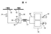
さらに、図4は、図1に示す実施例に係るプラズマ処理装置における静電吸着電極、直流電源及びこれらの間の給電線路の構成とその上を流れる電流とを模式的に示す図である。本図では、図3と同様に、正電位にされたタングステン電極15およびこれに接続された給電線路22を流れる高周波電流31は直流電源19に向けて、負電位にされたタングステン電極15およびこれに接続された給電線路22を流れる高周波電流32はタングステン電極15に向けて流れている状態を示している。
Further, FIG. 4 is a view schematically showing the configuration of the electrostatic attraction electrode, the DC power supply, the feed line between them and the current flowing thereon in the plasma processing apparatus according to the embodiment shown in FIG. In this figure, similarly to FIG. 3, the
この図において、高周波電流31は正電位にされたタングステン電極15と空芯巻きインダクタンス17との間の給電線路22に接続されたバイパス線路16’をコンデンサ16を介してバイパス電流33として通り、給電線路22上を通して負電位にされたタングステン電極15に接続された給電線路22に流入する。このため、コンデンサ16及びバイパス線路16’が接続されたことにより、高周波電流31がバイパスされるため、一方の空芯巻きインダクタンス17のコイル状部分に高周波電流32の流れている状態で位相の異なる高周波電流31が他方の空芯巻きインダクタンス17のコイル状部分に流入することが抑制される。このことにより、位相の異なる高周波電流が共通巻きのコイル状部分に流れることでインダクタンスの作用が相殺されたり損なわれたりすることが抑制される。
In this figure, the high frequency current 31 passes through the bypass line 16 'connected to the
一方、正負電位の各々にされたタングステン電極15の各々に流入する高周波電流はそれらの向きが同じでその大きさ、例えば振幅に差(電位差)がある場合においても、本実施例の構成では上記と同様の作用を奏することができる。
On the other hand, even if the high frequency current flowing into each of the
図5は、本実施例の比較例に係る静電吸着電極、直流電源及びこれらの間の給電線路の構成とその上を流れる電流とを模式的に示す図である。本図では、図3と同様に、コンデンサ16及びバイパス線路16’が2つの給電線路22同士の間を接続しておらず、正負電位の各々にされたタングステン電極15及びこれら各々に接続された給電線路22を流れる高周波電力はその位相が同じにされる一方でその振幅が異なり電位差がある場合を示している。各タングステン電極15と空芯巻きインダクタンスとの間の給電線路を流れる高周波電流31,32の流れる向きは図2と同じで高周波電流31の振幅が高周波電流32のものより大きくされている。
FIG. 5 is a view schematically showing the configuration of the electrostatic chucking electrode, the DC power supply, the feed line between them, and the current flowing thereon according to a comparative example of the present embodiment. In this figure, similarly to FIG. 3, the
この図の場合には、空芯巻きインダクタンス17を流れた振幅が大きな高周波電流31によって、線路間容量を介して逆向き電流34が生じる。この逆向き電流34により、振幅が小さな高周波電流32が流れる空芯巻きインダクタンス17の作用が抑制され、空芯巻きインダクタンス17でのインピーダンスが低下して高周波電流31または高周波電流32が流れる量を増加させてしまう。
In the case of this figure, the reverse current 34 is generated via the inter-line capacitance by the high frequency current 31 having a large amplitude flowing through the air
一方で、図6に示すように、本実施例では、コンデンサ16を備えるバイパス線路16’が空芯巻きインダクタンス17の前段で2つの給電線路22同士の間で接続されて配置されており、振幅が大きな高周波電流31の一部はバイパス線路16’にバイパス電流33として分かれて回路を流れて、さらに負電位にされたタングステン電極15に接続された給電線路22とバイパス線路16’との接続部から高周波電流32と合流して空芯巻きインダクタンス17、低域通過フィルタ18及び直流電源19に向けて流れることになる。このため、バイパス線路16’のコンデンサ16の分だけ2つの給電線路22間の電位差が低減される。
On the other hand, as shown in FIG. 6, in the present embodiment, the bypass line 16 'including the
このことにより、空芯巻きインダクタンス17に流入する高周波電流の量はこれらの差が小さくされて同等のものに近づけられる。このため、空芯巻きインダクタンス17の特性が揃えられたインダクタンスが2つの空芯巻きインダクタンス17のコイル状の部分に生起され、これらを流れて直流電源19に流れ込む高周波電流の量の線路ごとでのバラつきが低減されるという作用・効果が、2つの給電線路22を流れる高周波電力の電流の振幅に差がある、或いは高周波電力の電位差がある場合でも、奏される。
As a result, the amount of the high frequency current flowing into the air
以上述べてきたように、コンデンサ16を空芯巻きインダクタンス17の前段に配置することで、正負それぞれのタングステン電極15に流入する高周波電流の位相や振幅が相互に異なっていても、空芯巻きインダクタンス17のインピーダンスが損なわれることが抑制される。このことによって、静電吸着用の電極へ流入するプラズマ形成用の高周波電力の量の変動により、試料台2の静電吸着膜14上面上方に形成されるプラズマ11の密度や強度の大きさやその分布が、バラつきが変動することが抑制され、試料の処理の歩留まりが損なわれることが抑制される。
As described above, by arranging the
上記実施例では、双極型の静電吸着用の電極である複数(図2,4,6では2つ)のタングステン電極15の正負電位にされた各々に接続された給電線路22上に各々の線路が共通の軸回りに巻かれた(共通巻きとした)コイル状部分を備えた2つの空芯巻きインダクタンス17が配置されている。高周波電流が流れるコイル状部分のインダクタンスは、その内側の芯の部分にフェライト等透磁率が真空の空間または大気より高い材料の部材を用いることで高めることが可能である。一方で、プラズマ生成用の高周波電力として周波数がVHF帯またはそれより高いものが使用される場合では、このような高い透磁率の材料の部材が抵抗体として作用して高周波電力の損失が大きくなってしまい、結果としてより高いインピーダンスとこれによる作用が損なわれてしまう虞がある。
In the above embodiment, each of the
このことから、本実施例では上記静電吸着用の電極に接続された給電経路上に配置される素子として空芯巻きインダクタンス17を備えている。また、空芯巻きインダクタンス17の特性安定化や個体差を抑制するために、ポリテトラフルオロエチレン(PTFE)等の損失の小さい樹脂等の材料をコイル状の線路内側の芯または線路の固定ジグとして用いても良い。
From this, in the present embodiment, the air
図7は、図1に示す実施例の空芯巻きインダクタンスの構成の概略を模式的に示す縦断面図である。本実施例では、図7に示すように、空芯巻きインダクタンス17は、複数の給電線路22のうち正電位にされるタングステン電極15に接続された給電線路(正極側線路)35と負電位にされるタングステン電極15に接続された給電線路(負極側線路)36の一部が、これらを対として隣接して並べられて円筒形を有した固定ジグ37の上下方向の軸周りに上下の一方から他方に向けて円筒面に沿って巻きつけられて構成されている。プラズマ形成用の高周波電力の電流は、タングステン電極15を通してこのような構成を有するコイル状の部分の2つの給電線路35,36を共通の芯の部材である固定ジグ37の周囲に並行して流れることで、特性が揃えられたインダクタンスが形成され高周波電流の量の線路ごとでのバラつきが低減される。
FIG. 7 is a longitudinal sectional view schematically showing the outline of the configuration of the air core winding inductance of the embodiment shown in FIG. In the present embodiment, as shown in FIG. 7, the air-
本実施例の給電線路35,36は、PTFEを材料として構成された円筒形を有した固定ジグ37の円筒面上で上下方向軸回りに上下方向に延びて配置された螺旋状の溝の内側に挿入され、当該溝に沿って固定ジグ37に巻きつけられている。また、本例において、給電線路35と給電線路36とは銅芯線38の表面を絶縁性を有する樹脂等の材料で構成された絶縁被膜39で被覆されている。
The feed lines 35, 36 of the present embodiment are formed on the inside of a spiral groove which is vertically extended around an axis in the vertical direction on the cylindrical surface of a fixing
なお、コンデンサ16および空芯巻きインダクタンス17は、タングステン電極15からなるべく近い距離に配置されることが望ましい。コンデンサ16および空芯巻きインダクタンス17の箇所とタングステン電極15との間の給電線路22の長さが高周波電流の波長以上になると、当該給電線路22の寄生インピーダンスが流れる高周波電流の特性に影響を与えて変動が大きくなり試料台2上方の処理室40内に形成されるプラズマ11の密度や強度及びその分布の変動が大きくなって処理の再現性が損なわれてしまう虞がある。そこで、プラズマ生成用の高周波電力の周波数が200MHzであるので、タングステン電極15からコンデンサ16および空芯巻きインダクタンス17までの給電線路22の長さを高周波電力の電流の波長(1.5m)以下に、特には0.3mとされている。
The
空芯巻きインダクタンス17は、コイル状部分の寄生インピーダンス或いは寄生キャパシタンスに伴う自己共振特性を有し、通常インダクタンスとキャパシタンスの並列回路であらわせるインピーダンス特性を有している。給電線路22或いは給電線路35,36を流れる高周波電力の周波数が自己共振周波数と同じまたはこれに近い場合には並列共振が生じてしまい空芯巻きインダクタンス17においてインピーダンスが生起する。
The air-cored
しかしながら、このような共振によるインピーダンスは、コイル状部分を含む素子の構造や流れる高周波電力の周波数から受ける影響が大きく、これらの僅かな変動に対して急激に変化してしまう。このため本実施例では、空芯巻きインダクタンス17の自己共振周波数をプラズマ生成用の高周波電力のものに対して1.1倍以上または0.9倍以下とすることが好ましい。例えば、本実施例は、高周波電力の周波数が200MHzであるため空芯巻きインダクタンス17の自己共振周波数を240MHz近辺となるように構成することが望ましい。
However, the impedance due to such resonance is greatly affected by the structure of the element including the coiled portion and the frequency of the flowing high frequency power, and changes rapidly with these slight fluctuations. For this reason, in the present embodiment, it is preferable to set the self-resonant frequency of the air core wound
以上本実施例によれば、周波数が高いプラズマ生成用の高周波電力が双極型の静電吸着電極の回路へ流入したりその機差を抑制でき、プラズマ生成の変動および再現性の低下や装置間差の発生を抑制することが可能となり、歩留まりを向上させたプラズマ処理装置を提供することができる。 As described above, according to this embodiment, the high frequency power for plasma generation with high frequency can flow into the circuit of the bipolar electrostatic adsorption electrode or the machine difference thereof can be suppressed, and the fluctuation of plasma generation and the reduction of reproducibility and the inter-apparatus It is possible to suppress the occurrence of a difference, and a plasma processing apparatus with an improved yield can be provided.
なお、本発明は上記した実施例に限定されるものではなく、様々な変形例が含まれる。例えば、上記した実施例は本発明を分かりやすく説明するために詳細に説明したものであり、必ずしも説明した全ての構成を備えるものに限定されるものではない。また、ある構成の一部について、他の構成の追加・削除・置換をすることが可能である。 The present invention is not limited to the embodiments described above, but includes various modifications. For example, the embodiments described above are described in detail in order to explain the present invention in an easy-to-understand manner, and are not necessarily limited to those having all the configurations described. In addition, it is possible to add, delete, and replace another configuration for a part of one configuration.
本発明は、半導体装置の製造装置、特にリソグラフィー技術によって描かれたパタンをマスクに半導体材料のエッチング処理を行うプラズマエッチング装置に関する。本発明では、広域圧力でのプラズマ生成特性で優位なVHF帯以上の高周波にてプラズマを生成する場合に、プラズマ生成用高周波が試料設置手段内に設けられる静電吸着機能部への流入を効果的に阻止するフィルタを実現する。本発明の効果により、VHF帯以上の高周波をプラズマ生成に用いるプラズマ処理装置におけるプロセス再現性低下や装置間差の発生を大幅に抑制が実現できる。 The present invention relates to an apparatus for manufacturing a semiconductor device, and more particularly to a plasma etching apparatus for performing etching processing of a semiconductor material using a pattern drawn by lithography as a mask. In the present invention, when plasma is generated at a high frequency higher than the VHF band which is superior in plasma generation characteristics at wide pressure, the high frequency for plasma generation is effective to flow into the electrostatic adsorption function unit provided in the sample setting means. Implement a filter that blocks By the effect of the present invention, it is possible to significantly suppress the reduction in process reproducibility and the occurrence of inter-apparatus differences in a plasma processing apparatus using a high frequency band higher than the VHF band for plasma generation.
1…電磁コイル、2…試料台、2’…下部電極、3…試料、4…上部電極、5…シャワープレート、6…ガス導入ライン、7…上部電極温度制御手段、8…放電用高周波電源、9…放電用高周波電力整合器、10…真空容器、11…プラズマ、12…上部電極絶縁体、13…絶縁リング、14…静電吸着膜、15…タングステン電極、16…コンデンサ、16’…バイパス線路、17…空芯巻きインダクタンス、18…低域通過フィルタ、19…直流電源、20…バイアス用高周波電源、21…バイアス用高周波電力整合器、22…給電線路、23…絶縁体、24…サセプタ、25…冷媒通路、25’…配管、26…排気調節バルブ、27…排気口、28…試料設置手段の保持機構、29…給電経路、30…ヘリウム導入機構、30’…伝熱ガス供給路、31…高周波電流、32…高周波電流、33…バイパス電流、34…逆向き電流、35…給電線路(正極側線路)、36…給電線路(負極側線路)、37…PTFE製の空芯巻きインダクタンス固定ジグ、38…銅芯線、39…絶縁被膜、40…処理室。
DESCRIPTION OF
Claims (5)
置され前記プラズマを用いて処理される試料がその上に載せられる試料台と、この試料台
上面を構成してその上に前記試料が載せられる誘電体製の膜内に配置され当該試料を吸着
するための電力が供給されて異なる極性が形成される膜状の2つの電極と、当該2つの電
極と各々の電源との間の給電路上に配置され前記2つの電極各々に接続された2つの給電
線路が同じ軸回りに並列に巻かれたコイル状部分と、このコイル状部分と前記2つの電極
との間において前記2つの給電線路を接続しコンデンサを備えたバイパス線路とを備えた
プラズマ処理装置。 A processing chamber disposed inside the vacuum vessel and in which a plasma is formed; a sample stage disposed in the processing chamber on which a sample to be treated using the plasma is placed; Two film-like electrodes which are disposed in a dielectric film on which the sample is to be placed and which are supplied with electric power for adsorbing the sample to form different polarities, and the two electrodes, respectively A coiled portion in which two feed lines disposed on a feed path between the power supply and the feed line and connected to each of the two electrodes are wound in parallel around the same axis, the coiled portion and the two electrodes And a bypass line connected between the two feed lines and including a capacitor.
前記処理室内に前記プラズマを形成する電界を形成する高周波電力を供給する高周波電
源を有し、前記高周波電力の周波数が30乃至300MHzの範囲内であるプラズマ処理
装置。 The plasma processing apparatus according to claim 1,
A plasma processing apparatus, comprising: a high frequency power supply for supplying high frequency power for forming an electric field for forming the plasma in the processing chamber, wherein the frequency of the high frequency power is in a range of 30 to 300 MHz.
前記コイル状部分が内部に芯を有さないプラズマ処理装置。 The plasma processing apparatus according to claim 1 or 2, wherein
The plasma processing apparatus in which the said coiled part does not have a core inside.
前記コイル状部分が前記2つの給電線路上であって当該2つの給電線路の前記2つの電
極からの距離が前記高周波電力の電流の1波長以内に配置されたプラズマ処理装置。 The plasma processing apparatus according to claim 2, wherein
The plasma processing apparatus, wherein the coiled portion is on the two feed lines, and the distance from the two electrodes of the two feed lines is within one wavelength of the current of the high frequency power.
前記2つの給電線路上の前記コイル状部分と前記各々の電源との間に配置され前記高周
波電力を濾過するフィルタを備えたプラズマ処理装置。 The plasma processing apparatus according to claim 2 or 4, wherein
A plasma processing apparatus comprising a filter disposed between the coiled portions on the two feed lines and the respective power supplies for filtering the high frequency power.
Applications Claiming Priority (1)
| Application Number | Priority Date | Filing Date | Title |
|---|---|---|---|
| PCT/JP2017/011093 WO2018173095A1 (en) | 2017-03-21 | 2017-03-21 | Plasma treatment device |
Publications (2)
| Publication Number | Publication Date |
|---|---|
| JPWO2018173095A1 JPWO2018173095A1 (en) | 2019-04-04 |
| JP6530859B2 true JP6530859B2 (en) | 2019-06-12 |
Family
ID=63584322
Family Applications (1)
| Application Number | Title | Priority Date | Filing Date |
|---|---|---|---|
| JP2018511164A Active JP6530859B2 (en) | 2017-03-21 | 2017-03-21 | Plasma processing system |
Country Status (5)
| Country | Link |
|---|---|
| US (1) | US10825657B2 (en) |
| JP (1) | JP6530859B2 (en) |
| KR (1) | KR102056724B1 (en) |
| TW (1) | TWI701706B (en) |
| WO (1) | WO2018173095A1 (en) |
Families Citing this family (3)
| Publication number | Priority date | Publication date | Assignee | Title |
|---|---|---|---|---|
| CN111199860A (en) * | 2018-11-20 | 2020-05-26 | 江苏鲁汶仪器有限公司 | Etching uniformity adjusting device and method |
| KR102593142B1 (en) * | 2020-05-19 | 2023-10-25 | 세메스 주식회사 | Apparatus for treating substrate and method for controlling temperature of ferrite core |
| KR20220061617A (en) * | 2020-11-06 | 2022-05-13 | 세메스 주식회사 | Apparatus for treating substrate |
Family Cites Families (9)
| Publication number | Priority date | Publication date | Assignee | Title |
|---|---|---|---|---|
| JPS605539A (en) | 1983-06-23 | 1985-01-12 | Fujitsu Ltd | Electrostatic absorber |
| JP2685610B2 (en) * | 1989-12-07 | 1997-12-03 | 東京エレクトロン株式会社 | Plasma processing equipment |
| US5557215A (en) * | 1993-05-12 | 1996-09-17 | Tokyo Electron Limited | Self-bias measuring method, apparatus thereof and electrostatic chucking apparatus |
| JP3306677B2 (en) * | 1993-05-12 | 2002-07-24 | 東京エレクトロン株式会社 | Self-bias measurement method and device, and electrostatic suction device |
| JP6027374B2 (en) | 2012-09-12 | 2016-11-16 | 東京エレクトロン株式会社 | Plasma processing apparatus and filter unit |
| JP2016031955A (en) | 2014-07-28 | 2016-03-07 | 株式会社日立ハイテクノロジーズ | Plasma processing apparatus and plasma processing method |
| US9779919B2 (en) * | 2015-01-09 | 2017-10-03 | Hitachi High-Technologies Corporation | Plasma processing apparatus and plasma processing method |
| JP6567943B2 (en) * | 2015-01-09 | 2019-08-28 | 株式会社日立ハイテクノロジーズ | Plasma processing apparatus and plasma processing method |
| JP6650593B2 (en) * | 2017-02-17 | 2020-02-19 | パナソニックIpマネジメント株式会社 | Plasma processing apparatus and plasma processing method |
-
2017
- 2017-03-21 KR KR1020187003988A patent/KR102056724B1/en active IP Right Grant
- 2017-03-21 JP JP2018511164A patent/JP6530859B2/en active Active
- 2017-03-21 US US15/755,338 patent/US10825657B2/en active Active
- 2017-03-21 WO PCT/JP2017/011093 patent/WO2018173095A1/en active Application Filing
-
2018
- 2018-02-26 TW TW107106355A patent/TWI701706B/en active
Also Published As
| Publication number | Publication date |
|---|---|
| KR20180125432A (en) | 2018-11-23 |
| WO2018173095A1 (en) | 2018-09-27 |
| US10825657B2 (en) | 2020-11-03 |
| TWI701706B (en) | 2020-08-11 |
| JPWO2018173095A1 (en) | 2019-04-04 |
| US20200234924A1 (en) | 2020-07-23 |
| TW201843695A (en) | 2018-12-16 |
| KR102056724B1 (en) | 2019-12-17 |
Similar Documents
| Publication | Publication Date | Title |
|---|---|---|
| JP5643062B2 (en) | Plasma processing equipment | |
| JP5800547B2 (en) | Plasma processing apparatus and plasma processing method | |
| JP6027374B2 (en) | Plasma processing apparatus and filter unit | |
| US6265031B1 (en) | Method for plasma processing by shaping an induced electric field | |
| US9530619B2 (en) | Plasma processing apparatus and filter unit | |
| TWI611735B (en) | Plasma processing device (1) | |
| JP5309179B2 (en) | Plasma processing apparatus and coupling window configuration for producing uniform process speed | |
| KR101873485B1 (en) | Plasma processing apparatus | |
| US9218943B2 (en) | Plasma processing apparatus and plasma processing method | |
| TW201814407A (en) | Chamber with flow-through source | |
| US20150243486A1 (en) | Plasma processing apparatus | |
| US6850012B2 (en) | Plasma processing apparatus | |
| US9754766B2 (en) | Plasma processing apparatus | |
| JP6530859B2 (en) | Plasma processing system | |
| TW202004831A (en) | Plasma treatment apparatus | |
| JP6097317B2 (en) | Plasma processing method | |
| WO2020121588A1 (en) | Plasma treatment device | |
| JP6062461B2 (en) | Plasma processing equipment | |
| JP2016046357A (en) | Plasma processing device | |
| USRE40963E1 (en) | Method for plasma processing by shaping an induced electric field | |
| KR20020039638A (en) | Method and apparatus for plasma chemical treatment of a substrate surface |
Legal Events
| Date | Code | Title | Description |
|---|---|---|---|
| A521 | Written amendment |
Free format text: JAPANESE INTERMEDIATE CODE: A523 Effective date: 20180227 |
|
| A621 | Written request for application examination |
Free format text: JAPANESE INTERMEDIATE CODE: A621 Effective date: 20180227 |
|
| A131 | Notification of reasons for refusal |
Free format text: JAPANESE INTERMEDIATE CODE: A131 Effective date: 20181106 |
|
| A521 | Written amendment |
Free format text: JAPANESE INTERMEDIATE CODE: A523 Effective date: 20181227 |
|
| TRDD | Decision of grant or rejection written | ||
| A01 | Written decision to grant a patent or to grant a registration (utility model) |
Free format text: JAPANESE INTERMEDIATE CODE: A01 Effective date: 20190423 |
|
| A61 | First payment of annual fees (during grant procedure) |
Free format text: JAPANESE INTERMEDIATE CODE: A61 Effective date: 20190517 |
|
| R150 | Certificate of patent or registration of utility model |
Ref document number: 6530859 Country of ref document: JP Free format text: JAPANESE INTERMEDIATE CODE: R150 |
|
| S531 | Written request for registration of change of domicile |
Free format text: JAPANESE INTERMEDIATE CODE: R313531 |
|
| S533 | Written request for registration of change of name |
Free format text: JAPANESE INTERMEDIATE CODE: R313533 |
|
| R350 | Written notification of registration of transfer |
Free format text: JAPANESE INTERMEDIATE CODE: R350 |