JP2004014677A - Transmission apparatus using plastic fiber - Google Patents
Transmission apparatus using plastic fiber Download PDFInfo
- Publication number
- JP2004014677A JP2004014677A JP2002164038A JP2002164038A JP2004014677A JP 2004014677 A JP2004014677 A JP 2004014677A JP 2002164038 A JP2002164038 A JP 2002164038A JP 2002164038 A JP2002164038 A JP 2002164038A JP 2004014677 A JP2004014677 A JP 2004014677A
- Authority
- JP
- Japan
- Prior art keywords
- temperature
- plastic fiber
- light emitting
- semiconductor light
- emitting element
- Prior art date
- Legal status (The legal status is an assumption and is not a legal conclusion. Google has not performed a legal analysis and makes no representation as to the accuracy of the status listed.)
- Pending
Links
Images


Classifications
-
- G—PHYSICS
- G02—OPTICS
- G02B—OPTICAL ELEMENTS, SYSTEMS OR APPARATUS
- G02B6/00—Light guides; Structural details of arrangements comprising light guides and other optical elements, e.g. couplings
- G02B6/24—Coupling light guides
- G02B6/42—Coupling light guides with opto-electronic elements
- G02B6/4201—Packages, e.g. shape, construction, internal or external details
-
- G—PHYSICS
- G02—OPTICS
- G02B—OPTICAL ELEMENTS, SYSTEMS OR APPARATUS
- G02B6/00—Light guides; Structural details of arrangements comprising light guides and other optical elements, e.g. couplings
- G02B6/24—Coupling light guides
- G02B6/42—Coupling light guides with opto-electronic elements
- G02B6/43—Arrangements comprising a plurality of opto-electronic elements and associated optical interconnections
-
- B—PERFORMING OPERATIONS; TRANSPORTING
- B41—PRINTING; LINING MACHINES; TYPEWRITERS; STAMPS
- B41J—TYPEWRITERS; SELECTIVE PRINTING MECHANISMS, i.e. MECHANISMS PRINTING OTHERWISE THAN FROM A FORME; CORRECTION OF TYPOGRAPHICAL ERRORS
- B41J2/00—Typewriters or selective printing mechanisms characterised by the printing or marking process for which they are designed
- B41J2/435—Typewriters or selective printing mechanisms characterised by the printing or marking process for which they are designed characterised by selective application of radiation to a printing material or impression-transfer material
- B41J2/447—Typewriters or selective printing mechanisms characterised by the printing or marking process for which they are designed characterised by selective application of radiation to a printing material or impression-transfer material using arrays of radiation sources
- B41J2/46—Typewriters or selective printing mechanisms characterised by the printing or marking process for which they are designed characterised by selective application of radiation to a printing material or impression-transfer material using arrays of radiation sources characterised by using glass fibres
-
- G—PHYSICS
- G02—OPTICS
- G02B—OPTICAL ELEMENTS, SYSTEMS OR APPARATUS
- G02B6/00—Light guides; Structural details of arrangements comprising light guides and other optical elements, e.g. couplings
- G02B6/24—Coupling light guides
- G02B6/42—Coupling light guides with opto-electronic elements
- G02B6/4201—Packages, e.g. shape, construction, internal or external details
- G02B6/4266—Thermal aspects, temperature control or temperature monitoring
- G02B6/4268—Cooling
- G02B6/4271—Cooling with thermo electric cooling
-
- G—PHYSICS
- G02—OPTICS
- G02B—OPTICAL ELEMENTS, SYSTEMS OR APPARATUS
- G02B6/00—Light guides; Structural details of arrangements comprising light guides and other optical elements, e.g. couplings
- G02B6/02—Optical fibres with cladding with or without a coating
-
- G—PHYSICS
- G02—OPTICS
- G02B—OPTICAL ELEMENTS, SYSTEMS OR APPARATUS
- G02B6/00—Light guides; Structural details of arrangements comprising light guides and other optical elements, e.g. couplings
- G02B6/24—Coupling light guides
- G02B6/42—Coupling light guides with opto-electronic elements
- G02B6/4201—Packages, e.g. shape, construction, internal or external details
- G02B6/4246—Bidirectionally operating package structures
-
- H—ELECTRICITY
- H01—ELECTRIC ELEMENTS
- H01S—DEVICES USING THE PROCESS OF LIGHT AMPLIFICATION BY STIMULATED EMISSION OF RADIATION [LASER] TO AMPLIFY OR GENERATE LIGHT; DEVICES USING STIMULATED EMISSION OF ELECTROMAGNETIC RADIATION IN WAVE RANGES OTHER THAN OPTICAL
- H01S5/00—Semiconductor lasers
- H01S5/02—Structural details or components not essential to laser action
- H01S5/022—Mountings; Housings
- H01S5/0225—Out-coupling of light
- H01S5/02251—Out-coupling of light using optical fibres
-
- H—ELECTRICITY
- H01—ELECTRIC ELEMENTS
- H01S—DEVICES USING THE PROCESS OF LIGHT AMPLIFICATION BY STIMULATED EMISSION OF RADIATION [LASER] TO AMPLIFY OR GENERATE LIGHT; DEVICES USING STIMULATED EMISSION OF ELECTROMAGNETIC RADIATION IN WAVE RANGES OTHER THAN OPTICAL
- H01S5/00—Semiconductor lasers
- H01S5/02—Structural details or components not essential to laser action
- H01S5/022—Mountings; Housings
- H01S5/0233—Mounting configuration of laser chips
- H01S5/0234—Up-side down mountings, e.g. Flip-chip, epi-side down mountings or junction down mountings
-
- H—ELECTRICITY
- H01—ELECTRIC ELEMENTS
- H01S—DEVICES USING THE PROCESS OF LIGHT AMPLIFICATION BY STIMULATED EMISSION OF RADIATION [LASER] TO AMPLIFY OR GENERATE LIGHT; DEVICES USING STIMULATED EMISSION OF ELECTROMAGNETIC RADIATION IN WAVE RANGES OTHER THAN OPTICAL
- H01S5/00—Semiconductor lasers
- H01S5/02—Structural details or components not essential to laser action
- H01S5/024—Arrangements for thermal management
- H01S5/02453—Heating, e.g. the laser is heated for stabilisation against temperature fluctuations of the environment
-
- H—ELECTRICITY
- H01—ELECTRIC ELEMENTS
- H01S—DEVICES USING THE PROCESS OF LIGHT AMPLIFICATION BY STIMULATED EMISSION OF RADIATION [LASER] TO AMPLIFY OR GENERATE LIGHT; DEVICES USING STIMULATED EMISSION OF ELECTROMAGNETIC RADIATION IN WAVE RANGES OTHER THAN OPTICAL
- H01S5/00—Semiconductor lasers
- H01S5/06—Arrangements for controlling the laser output parameters, e.g. by operating on the active medium
- H01S5/0607—Arrangements for controlling the laser output parameters, e.g. by operating on the active medium by varying physical parameters other than the potential of the electrodes, e.g. by an electric or magnetic field, mechanical deformation, pressure, light, temperature
- H01S5/0612—Arrangements for controlling the laser output parameters, e.g. by operating on the active medium by varying physical parameters other than the potential of the electrodes, e.g. by an electric or magnetic field, mechanical deformation, pressure, light, temperature controlled by temperature
-
- H—ELECTRICITY
- H01—ELECTRIC ELEMENTS
- H01S—DEVICES USING THE PROCESS OF LIGHT AMPLIFICATION BY STIMULATED EMISSION OF RADIATION [LASER] TO AMPLIFY OR GENERATE LIGHT; DEVICES USING STIMULATED EMISSION OF ELECTROMAGNETIC RADIATION IN WAVE RANGES OTHER THAN OPTICAL
- H01S5/00—Semiconductor lasers
- H01S5/06—Arrangements for controlling the laser output parameters, e.g. by operating on the active medium
- H01S5/068—Stabilisation of laser output parameters
- H01S5/06804—Stabilisation of laser output parameters by monitoring an external parameter, e.g. temperature
Abstract
Description
【0001】
【発明の属する技術分野】
本発明は、光通信システム等に利用される、プラスチックファイバーを用いた伝送装置に関するものである。
【0002】
【従来の技術】
一般的に、光通信における光の伝搬路としては、石英ガラスを主材料としたシングルモード型、もしくはマルチモードファイバーが用いられる。これらのファイバーの直径は200μm以下であり、アライメントにおいてもミクロン単位の高い位置合わせ精度が求められる。そのため、工事現場等の一般環境下におけるファイバー敷設作業は容易ならざるものがあり、この点が、さらなる普及を妨げる大きな要因となっている。
【0003】
その一方、敷設作業が比較的容易になされ得る大直径のプラスチックファイバーも開発されているが、これらは製造上の問題から主にステップインデックス型の構造を有し、高いビットレートの信号を遠距離まで伝送することができない。つまり、ステップインデックス型のファイバーに光パルスを入力させた場合は、長距離の伝搬後に、出射端で光パルスの波形が崩れて広がってしまう現象が認められる。そのため、連続したパルスを伝送させると、時間軸上で前後のパルスが重なりあって、ファイバーの出射端面において、0レベルにおいても完全に消光しない状態となる。言い換えれば、短いパルス幅の信号列は伝送後、信号の0,1の判定がし難くなるということであり、大容量の光通信には不向きであることが分かる(「プラスチックオプティカルファイバの基礎と実際」小池康博、宮田清蔵 監修、株式会社エヌ・ティー・エス、pp.84−87 (2000)参照)。
【0004】
【発明が解決しようとする課題】
そこで、上述の問題を解消するために、大きな直径を有し、かつ、伝送後もパルス幅の広がらないグレーデッドインデックス(分布屈折率)型のファイバーが提案され、実用化が期待されているが、一方でその種のファイバーにおいては以下の問題が明らかになってきた。
【0005】
フッ化物を用いたプラスチックファイバー(商品名ルキナ、旭硝子株式会社)が実用化されているが、フッ化物は原材料が高価であるため低コスト化が困難で、またコア径を大きくすると使用するフッ化物の量が増すため更にコストが上がり、低コストで大口径コアによる敷設作業の容易さが特長であるプラスチックファイバーの利点を活かすことができない。
【0006】
一方、安価でコアの大口径化が容易な材料としてポリメチルメタクリレート(PMMA)が知られており、これを主たるコア材料としてグレーデッドインデックス型の光ファイバーを作製することが考えられている。しかしながら、PMMAを主成分とするコアを有するファイバーにおいて、伝搬損失の低い波長域は図6(文献:”POF−polymer optical fibers for data communication” Springer−Verlag(2002)から引用)に示すように、可視領域の中のごく限られた範囲(520nm、570nm、650nmの付近)に存在する。
【0007】
これらの中で、高速変調可能な半導体レーザあるいはLEDが作成可能な波長域は、現在のところ650nm付近の領域のみである。その他のより短波長の領域でも、II−VI族化合物半導体を用いたレーザの研究が行われているが、実用に耐える信頼性が得られる目処は立っていない。650nm付近の低損失の波長域において、630〜680nmの領域では略300dB/km以下の低損失特性が得られ、特に640〜660nmの狭い領域では略200dB/km以下の更なる低損失特性が得られる。この狭い領域外の例えば660nmよりやや長波長の光を用いる場合においては、伝搬損失が波長に応じて大きく変化するため、光源の波長が変化すると伝送装置の特性が変化してしまう。このような分散の大きな伝送特性を、新たな材料を適用することによって改善することも可能であるが、ファイバーのコストは通常のPMMAを用いる場合より上がってしまう。
【0008】
他方、上記650nm近傍の波長の光を発し、通信に必要な1mW程度の光量が得られ、そして400MHzから1GHz以上までの高速変調が可能な光源としては、DVDなどで用いられている端面発光型の半導体レーザが、高温下での発振の安定性、信頼性において最も優れている。しかしながら、この種の半導体レーザをプラスチックファイバーと組み合わせて光伝送に用いる場合、ファブリペロ共振器型レーザの問題として、発振波長が温度に応じてシフトするという問題がある。これは、半導体のエネルギーギャップが温度依存性を有する本質に由来するものであり、発振波長の変化は、
【数1】

【0009】
650nm帯の半導体レーザにおける実際の波長の温度依存性は約0.2nm/degである。したがって、環境温度が100℃上昇すると、発振波長は約20nm長波長側へシフトする。半導体レーザを作製するときの絶対波長のばらつきも±5nm程度あるので、上記シフトと合わせると30nmの範囲をカバーする必要があるが、図6のような伝搬特性を有するプラスチックファイバーでは損失が増大する可能性があるため、例えば使用する距離が限定されてしまう。
【0010】
このような場合、幹線系の光通信で採用されているペルチェ素子を用いて加熱・冷却により温度を一定に保つことにより、上記問題を解決することが可能であるが、その場合は、ペルチェ素子が高価であることから伝送装置のコスト上昇を招く。
【0011】
本発明は上記の事情に鑑み、大口径のコアを形成可能なプラスチックファイバーと、出射光波長の温度依存性を有する半導体発光素子とを組み合わせてなる伝送装置において、大幅なコスト上昇を招くことなく、低損失の安定した伝送特性を実現することを目的とする。
【0012】
【課題を解決するための手段】
本発明によるプラスチックファイバーを用いた伝送装置は、
前述したようにPMMAを主成分とするコアを有するプラスチックファイバーと、
このプラスチックファイバーを伝搬させる光を発する半導体発光素子とを有するプラスチックファイバーを用いた伝送装置において、
上記半導体発光素子として、波長が630〜680nmの範囲にある光を発するものが用いられるとともに、
上記半導体発光素子を加熱する加熱手段と、この半導体発光素子の温度を検出する温度検出手段と、この温度検出手段が出力する温度検出信号に基づいて前記加熱手段の駆動を制御して上記半導体発光素子の温度を、それが配置される環境において想定される最高温度よりも低い所定の目標値に設定する制御回路とからなる温度調節機構が設けられたことを特徴とするものである。
【0013】
なお上記半導体発光素子として、より好ましくは、波長が640〜660nmの範囲にある光を発するものが用いられる。
【0014】
またこの半導体発光素子は、端面発光型半導体レーザであることが望ましい。また別の観点からは、面発光型半導体レーザあるいは面発光型LEDが用いられることも好ましい。
【0015】
他方、前記プラスチックファイバーとしては、分布屈折率型のものが用いられることが望ましい。
【0016】
【発明の効果】
本発明のプラスチックファイバーを用いた伝送装置においては、PMMAを主成分とするコアを有するプラスチックファイバーにおいて、略300dB/km以下の低損失特性が得られる波長630〜680nmの範囲にある光を発する半導体発光素子が用いられていることにより、伝搬損失が低く抑えられるようになる。特に、640〜660nmの範囲にある光を発する半導体発光素子が用いられる場合は、さらに低い略200dB/km以下の低損失特性が得られるので、より好ましい。
【0017】
また、本発明によるプラスチックファイバーを用いた伝送装置においては、前述の通りの加熱手段と、温度検出手段と、制御回路とからなる温度調節機構により、半導体発光素子の温度を所定の目標値に設定するようにしているので、半導体発光素子が発する光の波長変動を狭い範囲に抑えて、光波長がプラスチックファイバーの低損失特性が得られる領域から外れることを防止し、常に低損失の安定した伝送特性を実現できる。そこで本発明によれば、高速・大容量の光通信が可能な距離を大幅に伸ばすことが可能となる。
【0018】
そして上記温度調節機構には、冷却作用を有するペルチェ素子等の高価な素子を用いずに、加熱手段を用いて半導体発光素子の温度を所定の目標値に設定するようにしているので、本発明のプラスチックファイバーを用いた伝送装置は、大幅なコスト上昇を招くことなく安定した伝送特性を実現できようになる。
【0019】
その上、上記温度調節機構は、半導体発光素子の温度を、それが配置される環境において想定される最高温度よりも低い所定の目標値に設定するように構成されているので、加熱手段を用いて半導体発光素子の温度をこの最高温度あるいはそれよりも高い目標値に設定する場合と比べれば、温度調節機構が簡略化され、装置コストの上昇を抑える効果はより顕著となる。さらに、高温で加速される光源の劣化や、モジュール部品の信頼性の低下を懸念しなくて済むようにもなる。
【0020】
なお、本発明のプラスチックファイバーを用いた伝送装置においては、温度調節の目標値を上記の通りに設定していることにより、環境温度がかなり上昇した際には、半導体発光素子が温度調節されないということも当然起こり得る。しかしそのようになっても、発光波長範囲を前述の通りに限定した半導体発光素子を用いていることから、実用に足りる低損失特性を確保できる。この点に関しては、後述の実施の形態において具体的数値を示して詳しく説明する。
【0021】
【発明の実施の形態】
以下、図面を参照して本発明の実施の形態を詳細に説明する。
【0022】
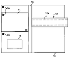
図1は、本発明の第1の実施形態によるプラスチックファイバーを用いた伝送装置の一部破断側面図である。ここに示される部分は光送信モジュール部を構成するものであり、図示の通りベースプレート1と、このベースプレート1に実装されたキャン型パッケージ2と、一端部がこのパッケージ2の中に挿通されたプラスチックファイバー3と、ベースプレート1の中に穿設された穴の中に配設されたサーミスタ4と、ステムの部分が上記ベースプレート1に取り付けられてパッケージ2の中に収納された端面発光型の半導体レーザ5と、同じくパッケージ2の中に収納されたボールレンズ6とを有している。またベースプレート1は電気ヒータ7を内蔵しており、この電気ヒータ7を上記サーミスタ4の出力信号に基づいて駆動する温度制御回路8が設けられている。
【0023】
上記半導体レーザ5は、温度25℃、出力3mWにおける発振波長が648nmで、発振波長の温度依存性が約0.2nm/degのものであり、直径5.6mmのキャン型パッケージ2に実装されている。プラスチックファイバー3はPMMAからなるコアを有するものであり、そのコア径は700μm、クラッドを含む直径は900μmである。半導体レーザ5から発せられたレーザ光9は、ボールレンズ6によりプラスチックファイバー3のコア3aの端面で収束するように集光されてコア3a内に入射し、そこをマルチモードで導波、伝搬する。
【0024】
半導体レーザ5の温度は、加熱手段としての電気ヒータ7と、温度検出手段としてのサーミスタ4と、温度制御回路8とからなる温度調節機構によって、所定の目標値に設定される。すなわち温度制御回路8は、サーミスタ4から出力される温度検出信号Sに基づいて電気ヒータ7の駆動電流を制御し、それによってベースプレート1の温度つまり半導体レーザ5の温度を目標値に維持する。
【0025】
なお上記温度調節の目標値は、使用環境において想定される最高温度よりも低い値とされる。ここでは、環境温度が例えば−45〜85℃の間の値を取り得るものと想定され、温度調節の目標値は35℃とされる。
【0026】
電気ヒータ7は半導体レーザ5を加熱するだけで、冷却することは不可能である。このような簡便な温度調節機構を用いる場合、上記のように温度調節の条件を設定すると、半導体レーザ5の温度は、環境温度が−45〜35℃の範囲では35℃に制御されるが、35℃を超えて85℃までの環境温度範囲では、環境温度そのままに変動することになる。
【0027】
しかし、温度調節を行なわない場合の半導体レーザ5の温度変化範囲は130℃であるのに対し、この温度調節を行なうことにより、温度変化範囲を50℃まで大幅に低減することができる。そこで、半導体レーザ5の発振波長の変動範囲も、約26nmから10nm程度までに抑えることができる。具体的にこの発振波長は、環境温度が−45〜35℃の範囲では約650nmに制御され、そして35〜85℃の範囲では約650〜660nmの範囲で変動する。
【0028】
以上のようにしてレーザ光9の波長変動範囲を小さく抑えることにより、図6に示したPMMAプラスチックファイバーの低損失領域を有効に使って、常に低損失の安定した伝送特性を実現できる。そこでこの伝送装置によれば、高速・大容量の光通信が可能な距離を大幅に伸ばすことが可能となる。
【0029】
また温度調節機構は、−45〜35℃の環境温度範囲でのみ半導体レーザ5の温度を目標値に制御し、35〜85℃の環境温度範囲では温度調節をしないものとされているので、比較的安価に形成することができる。それにより、本実施の形態の電送装置は、温度調節を行なうために大きくコストアップすることを回避できるものとなる。
【0030】
なお、端面発光型の半導体レーザ5は3mW以上の高出力が容易に得られ、更なる高出力化も可能であるため、ファイバー光学系の各種結合部の損失を含む伝送損失を出力向上により補償できることと、高温下での動作安定性が優れているために、加熱による温度調節により動作温度が比較的高温になっても安定して動作することの2点から、本発明において特に好適に用いられるものである。
【0031】
例えば、発振波長を645±5nm(35℃)として半導体レーザを作製するとき、上記実施の形態のように35〜85℃の間に動作範囲を限定すると、素子ばらつきと素子温度変化を考慮しても、640〜660nmの範囲に発振波長を限定することが可能となる。そこで、図6に示した伝搬損失特性のPMMAプラスチックファイバーを用いた場合には、略200dB/km以下の低損失領域を有効に利用することができる。具体的には、分布屈折率型のPMMAプラスチックファイバーを用いて、1GHz・100mの高速、長距離伝送も可能となる。
【0032】
なお、上記実施の形態ではボールレンズ6による集光方式を用いたが、集光用にボールレンズ以外のレンズを用いても構わない。また集光レンズは、予めキャン型パッケージ2の窓部に作り付けることも可能である。さらにプラスチックファイバーのコア径は700μmに限られるものではなく、それ以外に900μm等とされても構わない。本発明で使用するプラスチックファイバーはコア径を大きく形成できるので、そのファイバー端を半導体発光素子に近接配置することにより、レンズを用いずにレーザ光を直接ファイバーに結合させることも可能である。
【0033】
また、温度調節の目標値を常温より高めに設定することにより、各光学要素への結露を防止する効果も得られる。
【0034】
さらに、上記実施の形態では端面発光型半導体レーザを用いているが、本発明では面発光レーザも適用可能である。面発光レーザでは、発振波長の温度依存性がDBR(Distributed Bragg Reflector)ミラーの効果で、一般に端面発光型半導体レーザの1/3程度と小さく、温度調節しなくても発振波長を前記実施の形態におけるのと同様の範囲に収めることができる。しかし、図6に示すようなPMMAプラスチックファイバーの特に低損失の領域を有効に使うためには、更に狭い範囲に温度調節して使用することが好ましく、その観点から考えれば、本発明ではこの面発光レーザを適用することも好ましいと言える。同様に本発明では、DBRミラーを用いたLEDであるRC(Resonant Cavity)−LEDを適用することも可能である。
【0035】
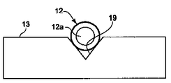
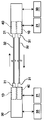
次に、本発明の別の実施の形態について説明する。図2は、本発明の第2の実施の形態によるプラスチックファイバーを用いた伝送装置の側面形状を示すものであり、また図3および図4は、この伝送装置のサブマウントから上の部分の平面形状および正面形状を示すものである。本実施の形態の伝送装置は、後述する図5の送受信モジュール30の送信サブモジュール10を構成するものであり、端面発光型の半導体レーザチップ11と、PMMAプラスチックファイバー12と、それらを固定するSi製のサブマウント13と、このSiサブマウント13を固定する、放熱板を兼ねたベースプレート14とを有している。
【0036】
半導体レーザチップ11は、温度25℃、出力3mWにおける発振波長が650nmで、発振波長の温度依存性が約0.2nm/degのものであり、その接合面、つまり活性層15に近い側の面を半田付けすることによって、Siサブマウント13上に固定されている。PMMAプラスチックファイバー12は、コア12aの径が500μm、クラッドを含む直径が700μmのものであり、半導体レーザチップ11から発せられたレーザ光16がそのコア12aの端面に直接照射されるように配置されている。それによりレーザ光16がコア12a内に入射し、そこをマルチモードで導波、伝搬する。
【0037】
Siサブマウント13の上面には、半導体レーザチップ11に近接させて、温度検出手段としてのサーミスタ17が固定されている。またSiサブマウント13の上面には、半導体レーザチップ11とPMMAプラスチックファイバー12とを分離する分離溝18が設けられるとともに、PMMAプラスチックファイバー12を位置決めするための断面V字形の溝19が設けられている。PMMAプラスチックファイバー12は、上記V溝19によって位置規定した後、UV硬化型接着剤によってSiサブマウント13に固定される。
【0038】
半導体レーザチップ11から出射するレーザ光16の広がり角度は半値全角で30度程度であり、上記分離溝18の幅を50〜100μm程度とすれば、レンズを用いなくても、レーザ光16を70%以上の効率でPMMAプラスチックファイバー12に結合させることができる。また、半導体レーザチップ11とSiサブマウント13にアライメントマーク20を設けておくことにより、PMMAプラスチックファイバー12を位置規定するV溝19と半導体レーザチップ11の発光位置とを位置合わせできるので、簡便な組立により高精度なアライメントが可能である。
【0039】
本実施の形態でも、第1の実施の形態におけるのと同様に半導体レーザチップ11の温度は、ベースプレート14に内蔵された加熱手段としての電気ヒータ22と、温度検出手段としてのサーミスタ17と、温度制御回路21とからなる温度調節機構によって、所定の目標値に設定される。すなわち温度制御回路21は、サーミスタ17から出力される温度検出信号Sに基づいて電気ヒータ22の駆動電流を制御し、それによってベースプレート14の温度つまり半導体レーザチップ11の温度を目標値に維持する。
【0040】
なお上記温度調節の目標値は、使用環境において想定される最高温度よりも低い値とされる。ここでも、環境温度が例えば−45〜85℃の間の値を取り得るものと想定され、温度調節の目標値は35℃とされる。このように温度調節の条件を設定すると、半導体レーザチップ11の温度は、環境温度が−45〜35℃の範囲では35℃に制御されるが、35℃を超えて85℃までの環境温度範囲では、環境温度そのままに変動することになる。
【0041】
しかし、温度調節を行なわない場合の半導体レーザチップ11の温度変化範囲は130℃であるのに対し、この温度調節を行なうことにより、温度変化範囲を50℃まで大幅に低減することができる。そこで、半導体レーザチップ11の発振波長の変動範囲も、約26nmから10nm程度までに抑えることができる。具体的にこの発振波長は、環境温度が−45〜35℃の範囲では約652nmに制御され、そして35〜85℃の範囲では約652〜662nmの範囲で変動する。
【0042】
以上のようにしてレーザ光16の波長変動範囲を小さく抑えることにより、図6に示したPMMAプラスチックファイバーの低損失領域を有効に使って、常に低損失の安定した伝送特性を実現できる。そこで本実施の形態においても、高速・大容量の光通信が可能な距離を大幅に伸ばすことが可能となる。
【0043】
なお本実施の形態において、半導体レーザチップ11の加熱はそれと別体のヒータにより行なっているが、半導体レーザチップ11の上にヒータを形成すれば、更に効率の高い加熱が可能となる。また、半導体レーザチップ11と別体のヒータを用いる場合は、それをベースプレート14中ではなく、Siサブマウント13の上等に設けても構わない。
【0044】
以上説明した送信サブモジュール10は、図5に示すように送受信モジュール30内に配置され、該サブモジュール10のPMMAプラスチックファイバー12(図5では省略)がコネクタ31を用いて伝送用PMMAプラスチックファイバー32に接続される。また各送受信モジュール30には、前述の温度制御回路21が接続されるとともに、送受信回路33が接続される。
【0045】
この例の場合には、双方向通信可能な送受信モジュール30内に、送信サブモジュール10に加えて受信用フォトダイオード等からなる受信サブモジュール40が配置され、その受信サブモジュール40もコネクタを31を用いて伝送用PMMAプラスチックファイバー32に接続される。つまり本例では、2つの送受信モジュール30がコネクタを31を介して2本のファイバー32によって接続されることにより、双方向光通信システムが構築される。
【0046】
上に説明した実施の形態では、モジュール内に伝送用のPMMAプラスチックファイバー32と同様のファイバー12を配して、それを半導体発光素子と結合させているが、本発明は伝送に用いるPMMAプラスチックファイバーの低損失特性を有効に活かして高性能な伝送装置を得るものであり、したがって、モジュール内部には必ずしも伝送に用いるのと同様の光ファイバーを用いる必要はなく、ガラスの光ファイバーや、外部のファイバーに適切に結合できるレンズ、導波路等の光学系を用いても構わない。
【0047】
また上記実施の形態では、サブモジュール内に加熱手段および温度検出手段を設けているが、サブモジュールを用いる装置によっては、サブモジュール外に加熱手段および温度検出手段を設けた方が良いことがある。さらに、他の目的に共用するため、あるいは複数のサブモジュールを同時に温度制御するために、外部に加熱手段および温度検出手段を設けても構わない。
【0048】
また本発明においては、PMMAのみからコアが形成されてなるプラスチックファイバーに限らず、PMMAに他の物質が添加された材料からコアが形成されてなるプラスチックファイバーを用いることも可能であり、その場合にも、プラスチックファイバーの損失特性は、損失の値自体は変化しても基本的に図6に示すパターンとなるから、先に説明したのと同様の効果を得ることができる。また本発明においては、PMMA以外の材料からコアが形成されてなるプラスチックファイバーでも、基本的に図6に示す損失特性を有するものであれば同様に適用可能である。
【0049】
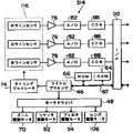
さらに、本発明によるプラスチックファイバーを用いた伝送装置は、一般的な光通信のみに限らず、情報を光信号によって伝送する全てのシステムに適用可能である。そのような光通信以外のシステムとしては、例えばディジタルラボシステムを挙げることが出来る。図7には、ディジタルラボシステム310の一例の概略構成が示されており、図8にはディジタルラボシステム310の外観が示されている。図7に示すように、このラボシステム310は、ラインCCDスキャナ314、画像処理部316、レーザプリンタ部318、及びプロセッサ部320を含んで構成されており、ラインCCDスキャナ314と画像処理部316は、図8に示す入力部326に設けられており、レーザプリンタ部318及びプロセッサ部320は、図8に示す出力部328に設けられている。
【0050】
ラインCCDスキャナ314は、ネガフィルムやリバーサルフィルム等の写真フィルムに記録されているフィルム画像を読み取るためのものであり、例えば135サイズの写真フィルム、110サイズの写真フィルム、及び透明な磁気層が形成された写真フィルム(240サイズの写真フィルム:いわゆるAPSフィルム)、120サイズ及び220サイズ(ブローニサイズ)の写真フィルムのフィルム画像を読取対象とすることができる。ラインCCDスキャナ314は、上記の読取対象のフィルム画像をラインCCDで読み取り、画像データを出力する。なお、上記のラインCCDスキャナ314に代えて、エリアCCDによってフィルム画像を読み取るエリアCCDスキャナを設けてもよい。
【0051】
画像処理部316は、ラインCCDスキャナ314から出力された画像データ(スキャン画像データ)が入力されると共に、デジタルカメラでの撮影によって得られた画像データ、フィルム画像以外の原稿(例えば反射原稿等)をスキャナで読み取ることで得られた画像データ、コンピュータで生成された画像データ等(以下、これらをファイル画像データと総称する)を外部から入力する(例えば、メモリカード等の記憶媒体を介して入力したり、通信回線を介して他の情報処理機器から入力する等)ことも可能なように構成されている。
【0052】
画像処理部316は、入力された画像データに対して各種の補正等の画像処理を行って、記録用画像データとしてレーザプリンタ部318へ出力する。また、画像処理部316は、画像処理を行った画像データを画像ファイルとして外部へ出力する(例えばメモリカード等の記憶媒体に出力したり、通信回線を介して他の情報処理機器へ送信する等)ことも可能である。
【0053】
レーザプリンタ部318はR、G、Bのレーザ光を発振するレーザ光源を備えており、画像処理部316から入力された記録用画像データに応じて変調したレーザ光を印画紙に照射して、走査露光によって印画紙に画像を記録する。また、プロセッサ部320は、レーザプリンタ部318で走査露光によって画像が記録された印画紙に対し、発色現像、漂白定着、水洗、乾燥の各処理を施す。これにより、印画紙上に画像が形成される。
【0054】
(ラインCCDスキャナの構成)次にラインCCDスキャナ314の構成について説明する。図9にはラインCCDスキャナ314の光学系の概略構成が示されている。この光学系は、ハロゲンランプやメタルハライドランプ等から成り写真フィルム322に光を照射する光源330を備えており、光源330の光射出側には、写真フィルム322に照射する光を拡散光とする光拡散ボックス336が配置されている。
【0055】
写真フィルム322は、光拡散ボックス336の光射出側に配置されたフィルムキャリア338(図11参照、図9では図示省略)によって光軸と直交する方向に搬送される。なお、図9では長尺状の写真フィルム322を示しているが、1コマ毎にスライド用のホルダに保持されたスライドフィルム(リバーサルフィルム)やAPSフィルムについては、各々専用のフィルムキャリアが用意されており(APSフィルム用のフィルムキャリアは磁気層に磁気記録された情報を読み取る磁気ヘッドを有している)、これらの写真フィルムを搬送することも可能である。
【0056】
また、光源330と光拡散ボックス336との間には、C(シアン)、M(マゼンタ)、Y(イエロー)の調光フィルタ114C、114M、114Yが射出光の光軸に沿って順に設けられており、写真フィルム322を挟んで光源330と反対側には、光軸に沿って、フィルム画像を透過した光を結像させるレンズユニット340、ラインCCD116が順に配置されている。図9ではレンズユニット340として単一のレンズのみを示しているが、レンズユニット340は、実際には複数枚のレンズから構成されたズームレンズである。
【0057】
ラインCCD116は、CCDセルから成る光電変換素子が一列に多数配置されかつ電子シャッタ機構が設けられたセンシング部が、間隔を空けて互いに平行に3ライン設けられており、各センシング部の光入射側にR、G、Bの色分解フィルタの何れかが各々取付けられて構成されている(いわゆる3ラインカラーCCD)。ラインCCD116は、各センシング部の受光面がレンズユニット340の結像位置に一致するように配置されている。また、各センシング部の近傍には、転送部が各センシング部に対応して各々設けられており、各センシング部の各CCDセルに蓄積された電荷は、対応する転送部を介して順に転送される。また図示は省略するが、ラインCCD116とレンズユニット340との間にはシャッタが設けられている。
【0058】
図10にはラインCCDスキャナ314の電気系の概略構成が示されている。ラインCCDスキャナ314は、ラインCCDスキャナ314全体の制御行なうマイクロプロセッサ46を備えている。マイクロプロセッサ46には、バス62を介してRAM64(例えばSRAM)、ROM66(例えば記憶内容を書換え可能なROM)が接続されると共に、モータドライバ48が接続されており、モータドライバ48にはフィルタ駆動モータ54が接続されている。フィルタ駆動モータ54は調光フィルタ114C、114M、114Yを各々独立にスライド移動させることが可能である。
【0059】
マイクロプロセッサ46は、図示しない電源スイッチのオンオフに連動して光源330を点消灯させる。また、マイクロプロセッサ46は、ラインCCD116によるフィルム画像の読み取り(測光)を行う際に、フィルタ駆動モータ54によって調光フィルタ114C、114M、114Yを各々独立にスライド移動させ、ラインCCD116に入射される光量を各成分色光毎に調節する。
【0060】
またモータドライバ48には、レンズユニット340の複数枚のレンズの位置を相対的に移動させることでレンズユニット340のズーム倍率を変更するズーム駆動モータ70、レンズユニット340全体を移動させることでレンズユニット340の結像位置を光軸に沿って移動させるレンズ駆動モータ106が接続されている。マイクロプロセッサ46は、フィルム画像のサイズやトリミングを行うか否か等に応じて、ズーム駆動モータ70によってレンズユニット340のズーム倍率を所望の倍率に変更する。
【0061】
一方、ラインCCD116にはタイミングジェネレータ74が接続されている。タイミングジェネレータ74は、ラインCCD116や後述するA/D変換器82等を動作させるための各種のタイミング信号(クロック信号)を発生する。ラインCCD116の信号出力端は、増幅器76を介してA/D変換器82に接続されており、ラインCCD116から出力された信号は、増幅器76で増幅されA/D変換器82でディジタルデータに変換される。
【0062】
A/D変換器82の出力端は、相関二重サンプリング回路(CDS)88を介してインタフェース(I/F)回路90に接続されている。CDS88では、フィードスルー信号のレベルを表すフィードスルーデータ及び画素信号のレベルを表す画素データを各々サンプリングし、各画素毎に画素データからフィードスルーデータを減算する。そして、演算結果(各CCDセルでの蓄積電荷量に正確に対応する画素データ)を、I/F回路90を介してスキャン画像データとして画像処理部316へ順次出力する。
【0063】
なお、ラインCCD116からはR、G、Bの測光信号が並列に出力されるので、増幅器76、A/D変換器82、CDS88から成る信号処理系も3系統設けられており、I/F回路90からは、スキャン画像データとしてR、G、Bの画像データが並列に出力される。
【0064】
また、モータドライバ48にはシャッタを開閉させるシャッタ駆動モータ92が接続されている。ラインCCD116の暗出力については、後段の画像処理部316で補正されるが、暗出力レベルは、フィルム画像の読み取りを行っていないときに、マイクロプロセッサ46がシャッタを閉止させることで得ることができる。
【0065】
(画像処理部の構成)次に画像処理部316の構成について図11を参照して説明する。画像処理部316は、ラインCCDスキャナ314に対応してラインスキャナ補正部122が設けられている。ラインスキャナ補正部122は、ラインCCDスキャナ314から並列に出力されるR、G、Bの画像データに対応して、暗補正回路124、欠陥画素補正部128、及び明補正回路130から成る信号処理系が3系統設けられている。
【0066】
暗補正回路124は、ラインCCD116の光入射側がシャッタにより遮光されている状態で、ラインCCDスキャナ314から入力されたデータ(ラインCCD116のセンシング部の各セルの暗出力レベルを表すデータ)を各セル毎に記憶しておき、ラインCCDスキャナ314から入力されたスキャン画像データから、各画素毎に対応するセルの暗出力レベルを減ずることによって補正する。
【0067】
また、ラインCCD116の光電変換特性は各セル単位で濃度のばらつきもある。欠陥画素補正部128の後段の明補正回路130では、ラインCCDスキャナ314に画面全体が一定濃度の調整用のフィルム画像がセットされている状態で、ラインCCD116で前記調整用のフィルム画像を読み取ることによりラインCCDスキャナ314から入力された調整用のフィルム画像の画像データ(この画像データが表す各画素毎の濃度のばらつきは各セルの光電変換特性のばらつきに起因する)に基づいて各セル毎にゲインを定めておき、ラインCCDスキャナ314から入力された読取対象のフィルム画像の画像データを、各セル毎に定めたゲインに応じて各画素毎に補正する。
【0068】
一方、調整用のフィルム画像の画像データにおいて、特定の画素の濃度が他の画素の濃度と大きく異なっていた場合には、ラインCCD116の前記特定の画素に対応するセルには何らかの異常があり、前記特定の画素は欠陥画素と判断できる。欠陥画素補正部128は調整用のフィルム画像の画像データに基づき欠陥画素のアドレスを記憶しておき、ラインCCDスキャナ314から入力された読取対象のフィルム画像の画像データのうち、欠陥画素のデータについては周囲の画素のデータから補間してデータを新たに生成する。
【0069】
また、ラインCCD116は写真フィルム322の搬送方向と直交する方向に延びた3本のライン(CCDセル列)が写真フィルム322の搬送方向に沿って所定の間隔を空けて順に配置されているので、ラインCCDスキャナ314からR、G、Bの各成分色の画像データの出力が開始されるタイミングには時間差がある。ラインスキャナ補正部122には、図示しない遅延回路が設けられており、フィルム画像上で同一の画素のR、G、Bの画像データが同時に出力されるように、最も遅く出力される画像データの出力タイミングを基準として残りの2色毎に異なる遅延時間で画像データの出力タイミングの遅延を行う。
【0070】
ラインスキャナ補正部122の出力端はセレクタ132の入力端に接続されており、補正部122から出力された画像データはセレクタ132に入力される。また、セレクタ132の入力端は入出力コントローラ134のデータ出力端にも接続されており、入出力コントローラ134からは、外部から入力されたファイル画像データがセレクタ132に入力される。セレクタ132の出力端は入出力コントローラ134、イメージプロセッサ部136A、136Bのデータ入力端に各々接続されている。セレクタ132は、入力された画像データを、入出力コントローラ134、イメージプロセッサ部136A、136Bの各々に選択的に出力可能とされている。
【0071】
イメージプロセッサ部136Aは、メモリコントローラ138、イメージプロセッサ140、3個のフレームメモリ142A、142B、142Cを備えている。フレームメモリ142A、142B、142Cは各々1フレーム分のフィルム画像の画像データを記憶可能な容量を有しており、セレクタ132から入力された画像データは3個のフレームメモリ142の何れかに記憶されるが、メモリコントローラ138は、入力された画像データの各画素のデータが、フレームメモリ142の記憶領域に一定の順序で並んで記憶されるように、画像データをフレームメモリ142に記憶させる際のアドレスを制御する。
【0072】
イメージプロセッサ140は、フレームメモリ142に記憶された画像データを取込み、階調変換、色変換、画像の超低周波輝度成分の階調を圧縮するハイパートーン処理、粒状を抑制しながらシャープネスを強調するハイパーシャープネス処理等の各種の画像処理を行う。なお、上記の画像処理の処理条件は、オートセットアップエンジン144(後述)によって自動的に演算され、演算された処理条件に従って画像処理が行われる。イメージプロセッサ140は入出力コントローラ134に接続されており、画像処理を行った画像データは、フレームメモリ142に一旦記憶された後に、所定のタイミングで入出力コントローラ134へ出力される。なお、イメージプロセッサ部136Bは、上述したイメージプロセッサ部136Aと同一の構成であるので説明を省略する。
【0073】
ラインCCDスキャナ314は、異なる解像度で2回の読み取りを行うこともできる。1回目の比較的低解像度での読み取り(以下、プレスキャンという)では、例えば、フィルム画像の濃度が極端に低い場合(例えばネガフィルムにおける露光オーバのネガ画像)にも、ラインCCD116で蓄積電荷の飽和が生じないように決定した読取条件(写真フィルムに照射する光のR、G、Bの各波長域毎の光量、CCDの電荷蓄積時間)でフィルム画像の読み取りが行われる。このプレスキャンによって得られた画像データ(プレスキャン画像データ)は、セレクタ132から入出力コントローラ134に入力され、更に入出力コントローラ134に接続されたオートセットアップエンジン144に出力される。
【0074】
オートセットアップエンジン144は、CPU146、RAM148(例えばDRAM)、ROM150(例えば記憶内容を書換え可能なROM)、入出力ポート152を備え、これらがバス154を介して互いに接続されて構成されている。
【0075】
オートセットアップエンジン144は、入出力コントローラ134から入力された複数コマ分のフィルム画像のプレスキャン画像データに基づいて、ラインCCDスキャナ314による2回目の比較的高解像度での読み取り(以下、ファインスキャンという)における光源330の光量を決定すると共に、ファインスキャンによって得られた画像データに対する画像処理の処理条件を演算し、演算した処理条件をイメージプロセッサ部136のイメージプロセッサ140へ出力する。この画像処理の処理条件の演算では、撮影時の露光量、撮影光源種やその他の特徴量から類似のシーンを撮影した複数のフィルム画像が有るか否か判定し、類似のシーンを撮影した複数のフィルム画像が有った場合には、これらのフィルム画像のファインスキャン画像データに対する画像処理の処理条件が同一又は近似するように決定する。
【0076】
なお、画像処理の最適な処理条件は、画像処理後の画像データを、レーザプリンタ部318における印画紙への画像の記録に用いるのか、外部へ出力するのか等によっても変化する。画像処理部316には2つのイメージプロセッサ部136A、136Bが設けられているので、例えば、画像データを印画紙への画像の記録に用いると共に外部へ出力する等の場合には、オートセットアップエンジン144は各々の用途に最適な処理条件を各々演算し、イメージプロセッサ部136A、136Bへ出力する。これにより、イメージプロセッサ部136A、136Bでは、同一のファインスキャン画像データに対し、互いに異なる処理条件で画像処理が行われる。
【0077】
さらに、オートセットアップエンジン144は、入出力コントローラ134から入力されたフィルム画像のプレスキャン画像データに基づいて、レーザプリンタ部318で印画紙に画像を記録する際のグレーバランス等を規定する画像記録用パラメータを算出し、レーザプリンタ部318に記録用画像データ(後述)を出力する際に同時に出力する。また、オートセットアップエンジン144は、外部から入力されるファイル画像データに対しても、上記と同様にして画像処理の処理条件を演算する。
【0078】
入出力コントローラ134はI/F回路156を介してレーザプリンタ部318に接続されている。画像処理後の画像データを印画紙への画像の記録に用いる場合には、イメージプロセッサ部136で画像処理が行われた画像データは、入出力コントローラ134からI/F回路156を介し記録用画像データとしてレーザプリンタ部318へ出力される。また、オートセットアップエンジン144はパーソナルコンピュータ158に接続されている。画像処理後の画像データを画像ファイルとして外部へ出力する場合には、イメージプロセッサ部136で画像処理が行われた画像データは、入出力コントローラ134からオートセットアップエンジン144を介してパーソナルコンピュータ158に出力される。
【0079】
パーソナルコンピュータ158は、CPU160、メモリ162、ディスプレイ164及びキーボード166(図8も参照)、ハードディスク168、CD−ROMドライバ170、搬送制御部172、拡張スロット174、画像圧縮/伸長部176を備えており、これらがバス178を介して互いに接続されて構成されている。搬送制御部172はフィルムキャリア338に接続されており、フィルムキャリア338による写真フィルム322の搬送を制御する。また、フィルムキャリア338にAPSフィルムがセットされた場合には、フィルムキャリア338がAPSフィルムの磁気層から読み取った情報(例えば画像記録サイズ等)が入力される。
【0080】
また、メモリカード等の記憶媒体に対してデータの読出し/書込みを行うドライバ(図示省略)や、他の情報処理機器と通信を行うための通信制御装置は、拡張スロット174を介してパーソナルコンピュータ158に接続される。入出力コントローラ134から外部への出力用の画像データが入力された場合には、前記画像データは拡張スロット174を介して画像ファイルとして外部(前記ドライバや通信制御装置等)に出力される。また、拡張スロット174を介して外部からファイル画像データが入力された場合には、入力されたファイル画像データは、オートセットアップエンジン144を介して入出力コントローラ134へ出力される。この場合、入出力コントローラ134では入力されたファイル画像データをセレクタ132へ出力する。
【0081】
なお、画像処理部316は、プレスキャン画像データ等をパーソナルコンピュータ158に出力し、ラインCCDスキャナ314で読み取られたフィルム画像をディスプレイ164に表示したり、印画紙に記録することで得られる画像を推定してディスプレイ164に表示し、キーボード166を介してオペレータにより画像の修正等が指示されると、これを画像処理の処理条件に反映することも可能とされている。
【0082】
図12にはレーザプリンタ部318及びプロセッサ部320の電気系の概略構成が示されている。レーザプリンタ部318は画像データを記憶するフレームメモリ230を備えている。フレームメモリ230はI/F回路232を介して画像処理部316に接続されており、画像処理部316から入力された記録用画像データ(印画紙224に記録すべき画像の各画素毎のR、G、B濃度を表す画像データ)はI/F回路232を介してフレームメモリ230に一旦記憶される。フレームメモリ230はD/A変換器234を介して露光部236に接続されると共に、プリンタ部制御回路238に接続されている。
【0083】
上記のようなディジタルラボシステムにおける情報をやりとりするいずれの部位にも、本発明装置は好適に使用できる。特に本発明装置は、ラインCCDスキャナから画像処理部へのデータ転送(図10の増幅器76−A/D変換器82間、A/D変換器82−CDS88間、CDS88−I/F回路90間)、画像処理部からレーザプリンタ部へのデータ転送(図12のA/D変換器234−露光部236間、フレームメモリ230−A/D変換器234間)、画像処理部から主制御(パーソナルコンピュータ)へのデータ転送(図11の入出力ポート152−バス178間)、主制御(パーソナルコンピュータ)から外部装置へのデータ転送(図7の画像処理部316−「記録媒体や他の情報処理機器等」間)、入力機から出力機へのデータ転送(図11の画像処理部316−レーザプリンタ部318間)等において光信号を伝送するために好ましく適用することができる。
【0084】
さらに本発明装置は、印刷製版工程における入力−編集(DTP)−出力の各工程間での情報伝送に、好適に使用することもできる。また本発明装置は、医療分野の情報伝送(例えば、病院内LAN、病院間LAN、より具体的には患者のカルテや医療診断画像を蓄積したセントラルサーバと各診察室の端末との間の情報伝送等)にも好適に使用することができる。
【図面の簡単な説明】
【図1】本発明の第1の実施形態によるプラスチックファイバーを用いた伝送装置を示す一部破断側面図
【図2】本発明の第2の実施形態によるプラスチックファイバーを用いた伝送装置を示す側面図
【図3】図3の伝送装置の一部を示す平面図
【図4】図3の伝送装置の一部を示す正面図
【図5】図3の伝送装置を用いた双方向光通信システムを示す概略図
【図6】本発明に用いられるPMMAプラスチックファイバーの伝搬損失特性を示すグラフ
【図7】本発明の伝送装置が適用され得るディジタルラボシステムの概略ブロック
【図8】上記ディジタルラボシステムの外観図
【図9】上記ディジタルラボシステムにおけるラインCCDスキャナの光学系の概略構成図
【図10】上記ラインCCDスキャナの電気系の概略構成を示すブロック図
【図11】上記ディジタルラボシステムにおける画像処理部の概略構成を示すブロック図
【図12】上記ディジタルラボシステムにおけるレーザプリンタ部及びプロセッサ部の電気系の概略構成を示すブロック図
【符号の説明】
1 ベースプレート
2 パッケージ
3 PMMAプラスチックファイバー
3a コア
4 サーミスタ
5 端面発光型半導体レーザ
6 ボールレンズ
7 電気ヒータ
8 温度制御回路
9 レーザ光
10 送信サブモジュール
11 端面発光型半導体レーザチップ
12 PMMAプラスチックファイバー
12a コア
13 Siサブマウント
14 ベースプレート
15 活性層
16 レーザ光
17 サーミスタ
20 アライメントマーク
21 温度制御回路
22 電気ヒータ
30 送受信モジュール
31 コネクタ
32 伝送用PMMAプラスチックファイバー
33 送受信回路
40 受信サブモジュール
76 増幅器
82 A/D変換器
88 CDS
90 I/F回路
152 入出力ポート
178 バス
230 フレームメモリ
234 A/D変換器
236 露光部
316 画像処理部
318 レーザプリンタ部[0001]
BACKGROUND OF THE INVENTION
The present invention relates to a transmission device using a plastic fiber used in an optical communication system or the like.
[0002]
[Prior art]
Generally, as a light propagation path in optical communication, a single mode type or multimode fiber mainly made of quartz glass is used. These fibers have a diameter of 200 μm or less, and high alignment accuracy in micron units is also required for alignment. Therefore, fiber laying work in a general environment such as a construction site is not easy, and this point is a major factor that hinders further spread.
[0003]
On the other hand, large-diameter plastic fibers that can be installed relatively easily have also been developed, but these have a step index type structure mainly due to manufacturing problems, and can transmit high bit rate signals over long distances. Cannot be transmitted. That is, when an optical pulse is input to a step index type fiber, a phenomenon is observed in which the waveform of the optical pulse collapses and spreads at the output end after propagation over a long distance. For this reason, when continuous pulses are transmitted, the preceding and succeeding pulses overlap on the time axis, and the emission end face of the fiber is not completely quenched even at the zero level. In other words, a signal train having a short pulse width makes it difficult to determine 0 or 1 of a signal after transmission, and is not suitable for large-capacity optical communication (see “Plastic Optical Fiber Basics”). Actually, "Yasuhiro Koike, supervised by Kiyozo Miyata, NTS Corporation, pp. 84-87 (2000)).
[0004]
[Problems to be solved by the invention]
Therefore, in order to solve the above-mentioned problems, a graded index (distributed refractive index) type fiber having a large diameter and having a pulse width that does not increase even after transmission has been proposed and is expected to be put to practical use. On the other hand, the following problems have been revealed in this type of fiber.
[0005]
Plastic fiber using fluoride (trade name Lucina, Asahi Glass Co., Ltd.) has been put to practical use, but fluoride is difficult to reduce costs because the raw materials are expensive, and the fluoride used when the core diameter is increased The cost increases further, and the advantage of the plastic fiber, which is low in cost and easy to lay with a large-diameter core, cannot be utilized.
[0006]
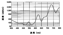
On the other hand, polymethyl methacrylate (PMMA) is known as a material that is inexpensive and can easily increase the diameter of the core, and it is considered that a graded index type optical fiber is produced using this as a main core material. However, in a fiber having a core mainly composed of PMMA, the wavelength range with low propagation loss is shown in FIG. 6 (reference: “POF-polymer optical fibers for data communication” Springer-Verlag (2002)). It exists in a very limited range in the visible region (near 520 nm, 570 nm, and 650 nm).
[0007]
Among these, the wavelength range in which a semiconductor laser or LED capable of high-speed modulation can be created is currently only a region around 650 nm. Research on lasers using II-VI group compound semiconductors has also been conducted in other shorter wavelength regions, but there is no prospect of obtaining reliability that can withstand practical use. In the low loss wavelength region near 650 nm, a low loss characteristic of approximately 300 dB / km or less is obtained in the region of 630 to 680 nm, and in particular, a further low loss characteristic of approximately 200 dB / km or less is obtained in the narrow region of 640 to 660 nm. It is done. When light having a wavelength slightly longer than 660 nm, for example, outside this narrow region is used, the propagation loss changes greatly depending on the wavelength, so that the characteristics of the transmission device change when the wavelength of the light source changes. Although it is possible to improve the transmission characteristics with such a large dispersion by applying a new material, the cost of the fiber is higher than that when using normal PMMA.
[0008]
On the other hand, as a light source that emits light having a wavelength in the vicinity of 650 nm, can obtain a light amount of about 1 mW necessary for communication, and can perform high-speed modulation from 400 MHz to 1 GHz or more, an edge-emitting type used in a DVD or the like. This semiconductor laser is most excellent in the stability and reliability of oscillation at a high temperature. However, when this type of semiconductor laser is used for optical transmission in combination with a plastic fiber, a problem with the Fabry-Perot resonator type laser is that the oscillation wavelength shifts with temperature. This is due to the fact that the energy gap of the semiconductor has temperature dependence, and the change in the oscillation wavelength is
[Expression 1]
[0009]
The temperature dependence of the actual wavelength in the 650 nm band semiconductor laser is about 0.2 nm / deg. Therefore, when the environmental temperature rises by 100 ° C., the oscillation wavelength shifts to the longer wavelength side by about 20 nm. Since the variation of absolute wavelength when manufacturing a semiconductor laser is about ± 5 nm, it is necessary to cover the range of 30 nm when combined with the shift, but the loss increases in the plastic fiber having the propagation characteristics as shown in FIG. Since there is a possibility, for example, the distance to be used is limited.
[0010]
In such a case, it is possible to solve the above problem by keeping the temperature constant by heating and cooling using a Peltier element employed in trunk-line optical communication. Is expensive, which increases the cost of the transmission apparatus.
[0011]
In view of the above circumstances, the present invention is a transmission device that combines a plastic fiber capable of forming a large-diameter core and a semiconductor light-emitting element having a temperature dependency of the outgoing light wavelength without causing a significant cost increase. The purpose is to realize a stable transmission characteristic with low loss.
[0012]
[Means for Solving the Problems]
A transmission device using a plastic fiber according to the present invention is:
As described above, a plastic fiber having a core mainly composed of PMMA,
In a transmission device using a plastic fiber having a semiconductor light emitting element that emits light propagating through the plastic fiber,
As the semiconductor light emitting element, one that emits light having a wavelength in the range of 630 to 680 nm is used.
Heating means for heating the semiconductor light emitting element; temperature detecting means for detecting the temperature of the semiconductor light emitting element; and driving of the heating means based on a temperature detection signal output from the temperature detecting means to control the semiconductor light emission. A temperature adjustment mechanism is provided, which includes a control circuit for setting the temperature of the element to a predetermined target value lower than the maximum temperature assumed in the environment in which the element is arranged.
[0013]
In addition, as the semiconductor light emitting element, a device that emits light having a wavelength in the range of 640 to 660 nm is more preferably used.
[0014]
The semiconductor light emitting device is preferably an edge emitting semiconductor laser. From another viewpoint, it is also preferable to use a surface emitting semiconductor laser or a surface emitting LED.
[0015]
On the other hand, it is desirable to use a distributed refractive index type plastic fiber.
[0016]
【The invention's effect】
In the transmission device using the plastic fiber of the present invention, a semiconductor that emits light in the wavelength range of 630 to 680 nm, which can obtain a low loss characteristic of approximately 300 dB / km or less, in a plastic fiber having a core mainly composed of PMMA. By using the light emitting element, the propagation loss can be suppressed low. In particular, when a semiconductor light emitting device that emits light in the range of 640 to 660 nm is used, it is more preferable because a lower loss characteristic of approximately 200 dB / km or less can be obtained.
[0017]
Further, in the transmission device using the plastic fiber according to the present invention, the temperature of the semiconductor light emitting element is set to a predetermined target value by the temperature adjusting mechanism including the heating unit, the temperature detection unit, and the control circuit as described above. Therefore, the wavelength variation of the light emitted from the semiconductor light-emitting element is suppressed to a narrow range, and the light wavelength is prevented from deviating from the region where the low loss characteristic of the plastic fiber can be obtained. The characteristics can be realized. Therefore, according to the present invention, it is possible to greatly extend the distance that enables high-speed and large-capacity optical communication.
[0018]
Since the temperature adjusting mechanism uses the heating means to set the temperature of the semiconductor light emitting element to a predetermined target value without using an expensive element such as a Peltier element having a cooling action, the present invention The transmission device using the plastic fiber can realize stable transmission characteristics without causing a significant cost increase.
[0019]
In addition, the temperature adjustment mechanism is configured to set the temperature of the semiconductor light emitting element to a predetermined target value lower than the highest temperature assumed in the environment in which the semiconductor light emitting element is disposed. Compared with the case where the temperature of the semiconductor light emitting element is set to the maximum temperature or a target value higher than that, the temperature adjustment mechanism is simplified, and the effect of suppressing the increase in device cost becomes more remarkable. Furthermore, there is no need to worry about the deterioration of the light source accelerated at high temperatures and the reliability of the module parts.
[0020]
In the transmission device using the plastic fiber of the present invention, the temperature adjustment target value is set as described above, so that the semiconductor light emitting element is not temperature adjusted when the environmental temperature is considerably increased. Of course this can happen. However, even in such a case, since the semiconductor light emitting element whose emission wavelength range is limited as described above is used, low loss characteristics sufficient for practical use can be secured. This point will be described in detail in the following embodiments with specific numerical values.
[0021]
DETAILED DESCRIPTION OF THE INVENTION
Hereinafter, embodiments of the present invention will be described in detail with reference to the drawings.
[0022]
FIG. 1 is a partially cutaway side view of a transmission device using plastic fibers according to a first embodiment of the present invention. The portion shown here constitutes an optical transmission module section. As shown in the figure, a base plate 1, a can-
[0023]
The
[0024]
The temperature of the
[0025]
The target value for temperature adjustment is set to a value lower than the maximum temperature assumed in the usage environment. Here, it is assumed that the environmental temperature can take a value between −45 and 85 ° C., for example, and the target value for temperature adjustment is 35 ° C.
[0026]
The
[0027]
However, the temperature change range of the
[0028]
As described above, by suppressing the wavelength fluctuation range of the laser light 9 to be small, a stable transmission characteristic with a low loss can always be realized by effectively using the low loss region of the PMMA plastic fiber shown in FIG. Therefore, according to this transmission apparatus, it is possible to greatly extend the distance that enables high-speed and large-capacity optical communication.
[0029]
The temperature adjustment mechanism controls the temperature of the
[0030]
The edge-emitting
[0031]
For example, when a semiconductor laser is manufactured with an oscillation wavelength of 645 ± 5 nm (35 ° C.), if the operating range is limited to 35 to 85 ° C. as in the above embodiment, element variation and element temperature change are taken into consideration. In addition, the oscillation wavelength can be limited to a range of 640 to 660 nm. Therefore, when the PMMA plastic fiber having the propagation loss characteristic shown in FIG. 6 is used, a low loss region of about 200 dB / km or less can be effectively used. Specifically, high-speed, long-distance transmission of 1 GHz · 100 m is possible using a distributed refractive index type PMMA plastic fiber.
[0032]
In the above embodiment, the condensing method using the ball lens 6 is used. However, a lens other than the ball lens may be used for condensing. The condensing lens can also be built in advance on the window portion of the can-
[0033]
Moreover, the effect which prevents the dew condensation on each optical element is also acquired by setting the target value of temperature control higher than normal temperature.
[0034]
Furthermore, although the edge emitting semiconductor laser is used in the above embodiment, a surface emitting laser is also applicable in the present invention. In the surface-emitting laser, the temperature dependency of the oscillation wavelength is generally about 1/3 of that of the edge-emitting semiconductor laser due to the effect of a distributed Bragg reflector (DBR) mirror, and the oscillation wavelength can be controlled without adjusting the temperature. Can be in the same range as in. However, in order to effectively use a particularly low-loss region of the PMMA plastic fiber as shown in FIG. 6, it is preferable to adjust the temperature to a narrower range. It can also be said that it is preferable to apply a light emitting laser. Similarly, in this invention, it is also possible to apply RC (Resonant Cavity) -LED which is LED using a DBR mirror.
[0035]
Next, another embodiment of the present invention will be described. FIG. 2 shows a side view of a transmission device using plastic fibers according to the second embodiment of the present invention, and FIGS. 3 and 4 are plan views of a portion above the submount of the transmission device. The shape and the front shape are shown. The transmission apparatus according to the present embodiment constitutes a
[0036]
The
[0037]
A
[0038]
The spread angle of the
[0039]
Also in this embodiment, the temperature of the
[0040]
The target value for temperature adjustment is set to a value lower than the maximum temperature assumed in the usage environment. Also here, it is assumed that the environmental temperature can take a value between −45 to 85 ° C., for example, and the target value for temperature adjustment is set to 35 ° C. When the temperature adjustment conditions are set in this way, the temperature of the
[0041]
However, the temperature change range of the
[0042]
As described above, by suppressing the wavelength fluctuation range of the
[0043]
In the present embodiment, the
[0044]
The
[0045]
In the case of this example, in addition to the
[0046]
In the embodiment described above, the
[0047]
In the above embodiment, the heating means and the temperature detection means are provided in the submodule. However, depending on the apparatus using the submodule, it may be better to provide the heating means and the temperature detection means outside the submodule. . Furthermore, a heating unit and a temperature detection unit may be provided outside in order to share them for other purposes or to control the temperature of a plurality of submodules simultaneously.
[0048]
In the present invention, not only the plastic fiber in which the core is formed only from PMMA, but also a plastic fiber in which the core is formed from a material in which another substance is added to PMMA can be used. In addition, since the loss characteristic of the plastic fiber basically has the pattern shown in FIG. 6 even if the loss value itself changes, the same effect as described above can be obtained. In the present invention, even a plastic fiber having a core formed of a material other than PMMA can be applied in the same manner as long as it has basically the loss characteristics shown in FIG.
[0049]
Furthermore, the transmission device using the plastic fiber according to the present invention is applicable not only to general optical communication but also to all systems that transmit information by optical signals. An example of such a system other than optical communication is a digital laboratory system. FIG. 7 shows a schematic configuration of an example of the
[0050]
The
[0051]
The
[0052]
The
[0053]
The
[0054]
(Configuration of Line CCD Scanner) Next, the configuration of the
[0055]
The
[0056]
Further, C (cyan), M (magenta), and Y (yellow) dimming
[0057]
In the
[0058]
FIG. 10 shows a schematic configuration of the electric system of the
[0059]
The
[0060]
The
[0061]
On the other hand, a
[0062]
An output terminal of the A /
[0063]
Since the
[0064]
The
[0065]
(Configuration of Image Processing Unit) Next, the configuration of the
[0066]
The dark correction circuit 124 receives data (data representing the dark output level of each cell of the sensing unit of the line CCD 116) input from the
[0067]
Further, the photoelectric conversion characteristics of the
[0068]
On the other hand, in the image data of the film image for adjustment, when the density of a specific pixel is significantly different from the density of other pixels, there is some abnormality in the cell corresponding to the specific pixel of the
[0069]
In addition, the
[0070]
The output end of the line
[0071]
The
[0072]
The
[0073]
The
[0074]
The auto setup engine 144 includes a CPU 146, a RAM 148 (for example, DRAM), a ROM 150 (for example, a ROM whose contents can be rewritten), and an input / output port 152, which are connected to each other via a
[0075]
The auto setup engine 144 reads the film image for a plurality of frames input from the input /
[0076]
The optimum processing conditions for image processing also vary depending on whether the image data after image processing is used for recording an image on photographic paper in the
[0077]
Further, the auto setup engine 144 is for image recording that defines a gray balance or the like for recording an image on photographic paper by the
[0078]
The input /
[0079]
The
[0080]
Also, a driver (not shown) for reading / writing data from / to a storage medium such as a memory card and a communication control device for communicating with other information processing devices are connected via a
[0081]
The
[0082]
FIG. 12 shows a schematic configuration of the electrical system of the
[0083]
The apparatus of the present invention can be suitably used for any part for exchanging information in the digital lab system as described above. Particularly, the apparatus of the present invention transfers data from the line CCD scanner to the image processing unit (between the
[0084]
Furthermore, the apparatus of the present invention can also be suitably used for information transmission between the input-editing (DTP) -output processes in the printing plate making process. In addition, the apparatus of the present invention transmits information in the medical field (for example, intra-hospital LAN, inter-hospital LAN, more specifically, information between a central server storing patient charts and medical diagnostic images and terminals in each examination room. Transmission) and the like.
[Brief description of the drawings]
FIG. 1 is a partially cutaway side view showing a transmission device using plastic fibers according to a first embodiment of the present invention.
FIG. 2 is a side view showing a transmission apparatus using plastic fibers according to a second embodiment of the present invention.
3 is a plan view showing a part of the transmission apparatus in FIG. 3;
4 is a front view showing a part of the transmission apparatus of FIG. 3;
FIG. 5 is a schematic diagram showing a bidirectional optical communication system using the transmission apparatus of FIG. 3;
FIG. 6 is a graph showing the propagation loss characteristics of the PMMA plastic fiber used in the present invention.
FIG. 7 is a schematic block diagram of a digital laboratory system to which the transmission apparatus of the present invention can be applied.
FIG. 8 is an external view of the digital lab system.
FIG. 9 is a schematic configuration diagram of an optical system of a line CCD scanner in the digital lab system.
FIG. 10 is a block diagram showing a schematic configuration of an electric system of the line CCD scanner.
FIG. 11 is a block diagram showing a schematic configuration of an image processing unit in the digital lab system.
FIG. 12 is a block diagram showing a schematic configuration of an electrical system of a laser printer unit and a processor unit in the digital lab system.
[Explanation of symbols]
1 Base plate
2 packages
3 PMMA plastic fiber
3a core
4 Thermistor
5 Edge-emitting semiconductor laser
6 ball lens
7 Electric heater
8 Temperature control circuit
9 Laser light
10 Transmission sub-module
11 Edge-emitting semiconductor laser chip
12 PMMA plastic fiber
12a core
13 Si submount
14 Base plate
15 Active layer
16 Laser light
17 Thermistor
20 Alignment mark
21 Temperature control circuit
22 Electric heater
30 transceiver module
31 connector
32 PMMA plastic fiber for transmission
33 Transmission / reception circuit
40 Receiving submodule
76 amplifier
82 A / D converter
88 CDS
90 I / F circuit
152 I / O port
178 bus
230 frame memory
234 A / D converter
236 Exposure section
316 Image processing unit
318 Laser printer section
Claims (5)
このプラスチックファイバーを伝搬させる光を発する半導体発光素子とを有するプラスチックファイバーを用いた伝送装置において、
前記半導体発光素子として、波長が630〜680nmの範囲にある光を発するものが用いられるとともに、
前記半導体発光素子を加熱する加熱手段と、この半導体発光素子の温度を検出する温度検出手段と、この温度検出手段が出力する温度検出信号に基づいて前記加熱手段の駆動を制御して前記半導体発光素子の温度を、それが配置される環境において想定される最高温度よりも低い所定の目標値に設定する制御回路とからなる温度調節機構が設けられたことを特徴とするプラスチックファイバーを用いた伝送装置。A plastic fiber having a core mainly composed of PMMA;
In a transmission device using a plastic fiber having a semiconductor light emitting element that emits light propagating through the plastic fiber,
As the semiconductor light emitting device, one that emits light having a wavelength in the range of 630 to 680 nm is used,
Heating means for heating the semiconductor light emitting element, temperature detecting means for detecting the temperature of the semiconductor light emitting element, and controlling the driving of the heating means based on a temperature detection signal output from the temperature detecting means to emit the semiconductor light Transmission using a plastic fiber, characterized in that a temperature control mechanism is provided comprising a control circuit for setting the temperature of the element to a predetermined target value lower than the maximum temperature assumed in the environment in which the element is arranged. apparatus.
Priority Applications (6)
| Application Number | Priority Date | Filing Date | Title |
|---|---|---|---|
| JP2002164038A JP2004014677A (en) | 2002-06-05 | 2002-06-05 | Transmission apparatus using plastic fiber |
| CNB031378633A CN1324338C (en) | 2002-06-05 | 2003-05-28 | Transmission apparatus using a plastic fiber |
| EP03012617A EP1369722A3 (en) | 2002-06-05 | 2003-06-03 | Transmission apparatus using a plastic fiber |
| TW092114980A TWI243260B (en) | 2002-06-05 | 2003-06-03 | Transmission device with plastic optical fiber |
| KR10-2003-0036279A KR20030094120A (en) | 2002-06-05 | 2003-06-05 | Transmission apparatus using plastic fiber |
| US10/454,601 US6874951B2 (en) | 2002-06-05 | 2003-06-05 | Transmission apparatus using a plastic fiber |
Applications Claiming Priority (1)
| Application Number | Priority Date | Filing Date | Title |
|---|---|---|---|
| JP2002164038A JP2004014677A (en) | 2002-06-05 | 2002-06-05 | Transmission apparatus using plastic fiber |
Publications (1)
| Publication Number | Publication Date |
|---|---|
| JP2004014677A true JP2004014677A (en) | 2004-01-15 |
Family
ID=29545768
Family Applications (1)
| Application Number | Title | Priority Date | Filing Date |
|---|---|---|---|
| JP2002164038A Pending JP2004014677A (en) | 2002-06-05 | 2002-06-05 | Transmission apparatus using plastic fiber |
Country Status (6)
| Country | Link |
|---|---|
| US (1) | US6874951B2 (en) |
| EP (1) | EP1369722A3 (en) |
| JP (1) | JP2004014677A (en) |
| KR (1) | KR20030094120A (en) |
| CN (1) | CN1324338C (en) |
| TW (1) | TWI243260B (en) |
Cited By (2)
| Publication number | Priority date | Publication date | Assignee | Title |
|---|---|---|---|---|
| JP2005244242A (en) * | 2004-02-25 | 2005-09-08 | Osram Opto Semiconductors Gmbh | Apparatus provided with at least one beam radiation semiconductor device, and method of stabilizing operating temperature of the beam radiation semiconductor device |
| JP2008016704A (en) * | 2006-07-07 | 2008-01-24 | Sony Corp | Manufacturing method and apparatus for semiconductor laser device |
Families Citing this family (6)
| Publication number | Priority date | Publication date | Assignee | Title |
|---|---|---|---|---|
| US7636522B2 (en) * | 2004-04-15 | 2009-12-22 | Infinera Corporation | Coolerless photonic integrated circuits (PICs) for WDM transmission networks and PICs operable with a floating signal channel grid changing with temperature but with fixed channel spacing in the floating grid |
| EP1648057A1 (en) * | 2004-10-13 | 2006-04-19 | Harman Becker Automotive Systems GmbH | Semiconductor laser device |
| KR100637930B1 (en) * | 2004-11-08 | 2006-10-24 | 한국전자통신연구원 | Wavelength tunable light source module for wavelength division multiplexed passive optical network system |
| DE102005009642B4 (en) * | 2005-03-03 | 2010-01-21 | Schott Ag | Optical signal pickup with beam shaping device |
| CN102809786A (en) * | 2011-06-01 | 2012-12-05 | 深圳市博特光通讯设备有限公司 | Package of electro-optical module for plastic optical fiber |
| TWI683073B (en) * | 2019-02-01 | 2020-01-21 | 達豐通訊科技股份有限公司 | Light box structure |
Family Cites Families (7)
| Publication number | Priority date | Publication date | Assignee | Title |
|---|---|---|---|---|
| US6152588A (en) * | 1994-09-28 | 2000-11-28 | Sdl, Inc. | Addressable vehicular lighting system |
| US6130444A (en) * | 1998-02-27 | 2000-10-10 | Nec Corporation | Optical fiber secured with a photosetting resin covered with a UV light-transmissive plate |
| US6244754B1 (en) * | 1998-03-30 | 2001-06-12 | Sumitomo Electric Industries, Ltd. | Semiconductor laser module and method of manufacturing the same |
| DE19817738C2 (en) * | 1998-04-21 | 2003-02-06 | Karl-Friedrich Klein | Hollow optical waveguide for trace analysis in aqueous solutions |
| JP2001094200A (en) * | 1999-09-21 | 2001-04-06 | Hitachi Ltd | Semiconductor laser module |
| JP2002171023A (en) * | 2000-11-30 | 2002-06-14 | Hitachi Ltd | Integrated optical element, semiconductor laser module, and optical transmission device |
| JP2002250846A (en) * | 2001-02-26 | 2002-09-06 | Seiko Epson Corp | Optical module, its manufacturing method and optical transmission device |
-
2002
- 2002-06-05 JP JP2002164038A patent/JP2004014677A/en active Pending
-
2003
- 2003-05-28 CN CNB031378633A patent/CN1324338C/en not_active Expired - Fee Related
- 2003-06-03 TW TW092114980A patent/TWI243260B/en not_active IP Right Cessation
- 2003-06-03 EP EP03012617A patent/EP1369722A3/en not_active Withdrawn
- 2003-06-05 KR KR10-2003-0036279A patent/KR20030094120A/en not_active Application Discontinuation
- 2003-06-05 US US10/454,601 patent/US6874951B2/en not_active Expired - Fee Related
Cited By (2)
| Publication number | Priority date | Publication date | Assignee | Title |
|---|---|---|---|---|
| JP2005244242A (en) * | 2004-02-25 | 2005-09-08 | Osram Opto Semiconductors Gmbh | Apparatus provided with at least one beam radiation semiconductor device, and method of stabilizing operating temperature of the beam radiation semiconductor device |
| JP2008016704A (en) * | 2006-07-07 | 2008-01-24 | Sony Corp | Manufacturing method and apparatus for semiconductor laser device |
Also Published As
| Publication number | Publication date |
|---|---|
| CN1467523A (en) | 2004-01-14 |
| EP1369722A3 (en) | 2004-06-30 |
| TWI243260B (en) | 2005-11-11 |
| TW200401127A (en) | 2004-01-16 |
| KR20030094120A (en) | 2003-12-11 |
| US6874951B2 (en) | 2005-04-05 |
| EP1369722A2 (en) | 2003-12-10 |
| US20030228113A1 (en) | 2003-12-11 |
| CN1324338C (en) | 2007-07-04 |
Similar Documents
| Publication | Publication Date | Title |
|---|---|---|
| US7576908B2 (en) | Fiber device, wavelength converter and image forming apparatus | |
| US6169562B1 (en) | Image exposure apparatus | |
| JP2004014677A (en) | Transmission apparatus using plastic fiber | |
| US7903325B2 (en) | Wavelength converter and image display device | |
| JP2001346002A (en) | Light source device and image reader | |
| JP3667990B2 (en) | Image reading device | |
| JP2008085038A (en) | Light-emitting element driving method and apparatus | |
| JP2001111782A (en) | Image reader | |
| JP2007147688A (en) | Wavelength conversion element, laser apparatus, and photographic processor | |
| US20100091150A1 (en) | Solid-state imaging device and signal processing system | |
| JP2003229636A (en) | Semiconductor laser element and semiconductor laser device | |
| JP2826222B2 (en) | Assembling method of semiconductor laser | |
| JP2001045225A (en) | Image reader | |
| JP2003218441A (en) | Light emitting unit | |
| Li et al. | Beam-curvature-compensated Solid-state Beam Scanner Integrated with Multi-grating Pitch Tunable Slow-light VCSELs for Enhanced Field of View | |
| JP2903269B2 (en) | Optical scanning device and photoreceptor | |
| JPH1198315A (en) | Picture reading device | |
| JP2000312278A (en) | Image reader | |
| JP2001326415A (en) | Optical module and light source device | |
| Dagenais et al. | Complex needs drive optoelectronic integration | |
| JP2005223040A (en) | Exposure light source, exposure device, and image forming device | |
| JP2002261386A (en) | Light emitting device, optical communication system and method for generating signal light | |
| JPH11313200A (en) | Image reader | |
| KITA et al. | Tunable Lasers: Quantum dots and silicon photonics combine in broadband tunable laser | |
| JP2004235590A (en) | Image forming apparatus |
Legal Events
| Date | Code | Title | Description |
|---|---|---|---|
| A621 | Written request for application examination |
Free format text: JAPANESE INTERMEDIATE CODE: A621 Effective date: 20050207 |
|
| A711 | Notification of change in applicant |
Free format text: JAPANESE INTERMEDIATE CODE: A712 Effective date: 20061205 |
|
| A131 | Notification of reasons for refusal |
Free format text: JAPANESE INTERMEDIATE CODE: A131 Effective date: 20071204 |
|
| A02 | Decision of refusal |
Free format text: JAPANESE INTERMEDIATE CODE: A02 Effective date: 20080401 |