JP2004014200A - Fluorescent display tube, and control electrode member of the same - Google Patents
Fluorescent display tube, and control electrode member of the same Download PDFInfo
- Publication number
- JP2004014200A JP2004014200A JP2002163476A JP2002163476A JP2004014200A JP 2004014200 A JP2004014200 A JP 2004014200A JP 2002163476 A JP2002163476 A JP 2002163476A JP 2002163476 A JP2002163476 A JP 2002163476A JP 2004014200 A JP2004014200 A JP 2004014200A
- Authority
- JP
- Japan
- Prior art keywords
- mesh
- grid electrode
- display tube
- fluorescent display
- grid
- Prior art date
- Legal status (The legal status is an assumption and is not a legal conclusion. Google has not performed a legal analysis and makes no representation as to the accuracy of the status listed.)
- Pending
Links
Images


Abstract
Description
【0001】
【発明の属する技術分野】
本発明は、蛍光表示管に関し、特にその制御電極の改良に関する。
【0002】
【従来の技術】
基板の表示面に所定形状で設けられた複数個の蛍光体層と、その蛍光体層の上方に架設されたフィラメント状陰極と、それら蛍光体層および陰極の間の高さ位置でその蛍光体層を覆う複数の制御電極とを備え、その陰極から発生させられた電子をその制御電極で制御してその蛍光体層に選択的に入射させることによりその蛍光体層を発光させる形式の蛍光表示管が知られている。このような蛍光表示管は低い動作電圧で鮮明に表示されると共に、発光色の異なる蛍光体層を用意することによりカラー表示が可能となる等の特徴がある為、音響機器や自動車の表示パネルの表示部品などとして多用されている。
【0003】
【発明が解決しようとする課題】
ところで、上記の制御電極は例えば金属製メッシュから成るものであり、異電極毎すなわち相互に独立したタイミングで制御される表示パターン毎に分割して基板の表示面に固定されていた。このような金属製メッシュは、例えばエッチング加工等によって複数個が1枚の金属薄板にまとめて形成され、プレスによる打ち抜き加工によって個々に分割されていた。そのため、複雑な輪郭形状を備えた表示パターンを設けようとしても、金属製メッシュを個々に分割するための金型の設計が困難であるため、表示パターン設計上の制約となっていた。また、複数の制御電極が個々に分割された状態で基板の表示面に固着されることから、固着位置のずれや欠落等の不具合が生じ易い問題もあった。
【0004】
本発明は、以上の事情を背景として為されたものであって、その目的は、複雑な表示パターンにも対応可能で制御電極の位置ずれや欠落等の生じ難い蛍光表示管およびその蛍光表示管を製造するための制御電極を提供することにある。
【0005】
【課題を解決するための第1の手段】
斯かる目的を達成するため、第1発明の蛍光表示管の要旨とするところは、基板の表示面に所定形状で設けられた複数個の蛍光体層と、その蛍光体層の上方に架設された陰極と、それら複数個の蛍光体層および陰極の間の高さ位置でそれら蛍光体層の各々を所定の発光区分毎に覆う複数の制御電極とを備え、その陰極から発生させられた電子をその制御電極で制御してその蛍光体層に入射させることによりその蛍光体層を選択的に発光させる形式の蛍光表示管であって、(a)前記蛍光体層および前記陰極の間の高さ位置に配置された絶縁体材料製の平坦な網目状部材と、(b)前記発光区分単位で相互に所定距離隔てて前記網目状部材上に区画された複数の領域毎にその網目状部材に積層された前記制御電極として機能させられる複数の導体層とを、含むことにある。
【0006】
【第1発明の効果】
このようにすれば、網目状部材に複数の領域毎に積層された導体層の各々が、相互に電気的に独立した複数の制御電極として機能させられる。そのため、この複数の導体層を備えた網目状部材(以下、制御電極部材という)には相対位置が固定された状態で複数の制御電極が備えられることから、その制御電極部材を基板の表示面に固定するだけで、網目状部材上における相対位置を保ちつつそれら複数の制御電極を同時に配置することができる。しかも、複数の制御電極すなわち複数の導体層はその相互の境界で電気的に分割されることになるため、網目状部材に設ける複数の導体層の各々の形状を適宜定めることによって、網目状部材の形状を矩形等の単純形状に保ったまま、実質的に所望の位置および形状で制御電極を分割することができる。したがって、複雑な表示パターンにも対応可能で制御電極の位置ずれや欠落等の生じ難い蛍光表示管が得られる。
【0007】
【課題を解決するための第2の手段】
また、前記目的を達成するための第2発明の制御電極部材の要旨とするところは、複数個の蛍光体層に向かう電子を所定の発光区分毎に制御する複数の制御電極を設けるために蛍光表示管の表示面にそれら複数個の蛍光体層を覆うように配置される制御電極部材であって、(a)絶縁体材料製の平坦な網目状部材と、その網目状部材上に区画された複数の領域毎に相互に所定距離隔ててその網目状部材に積層された前記制御電極として機能させられる複数の導体層とを含むことにある。
【0008】
【第2発明の効果】
このようにすれば、網目状部材には、制御電極として機能させられる導体層がその複数の領域毎に備えられるため、制御電極部材には、相対位置が一定に保たれた複数の制御電極が一体的に備えられることとなる。そのため、基板の表示面に設けられた複数個の蛍光体層により構成される発光区分に対応して上記領域を定めて制御電極部材を表示面に配設することにより、複数の制御電極をその相対位置を所期の位置に保ちつつ同時にその発光区分毎に設けることができる。このとき、網目状部材に積層される複数の制御電極すなわち導体層は、相互に所定距離隔てられることで電気的に絶縁させられることから、網目状部材の全体形状を矩形等の単純形状に保ちながら、所望の位置および形状で制御電極を分割することができる。すなわち、蛍光体層および発光区分を任意の平面形状で設け且つそれらの形状に応じた任意の形状で制御電極を設けることができる。したがって、複雑な表示パターンにも対応可能で配設する際の制御電極の位置ずれや欠落等の生じ難い制御電極部材が得られる。
【0009】
【発明の他の態様】
ここで、好適には、前記蛍光表示管または前記制御電極部材において、前記網目状部材は、前記蛍光体層上に位置する部分の開口率が他の部分の開口率よりも高められたものである。このようにすれば、蛍光体層上に配置される部分では相対的に開口率が高くされるため網目状部材による遮光が抑制されるが、他の部分では相対的に開口率が低くされることによって機械的強度が確保されるため、網目状部材全体の機械的強度が十分に高く保たれる。なお、開口率を高くするほど遮光が少なくなって輝度が高められると共に一般的には網目状部材の影が観察され難くなって表示品位が向上するが、その反面で蛍光体層の内周側における電子の制御が困難になる。このため、蛍光体層上に位置させられる部分の開口率は、電子の制御性と表示品位との兼ね合いで定めることが望ましい。
【0010】
また、好適には、前記網目状部材は、厚膜セラミック・シート、セラミック繊維製シート、エッチング・ガラス、ガラスクロス、或いは金属メッシュにガラスを電着した琺瑯から成るものである。これらのものは適当な開口率と機械的強度を備えているので好適に用いられる。なお、本願において「絶縁体材料製」とは、少なくとも表面において電気絶縁性を有する材料で構成されることを言うものである。
【0011】
また、好適には、前記導体層は、厚膜スクリーン印刷法を用いて前記網目状部材の一面に厚膜導体ペーストを所定パターンで塗布することによって形成された厚膜導体層である。このようにすれば、適宜の印刷パターンが形成されたスクリーンを用いることにより、所望の形状で分割された導体層を容易に設けることができる。すなわち、本発明によれば、矩形等の単純形状の網目状部材に導体パターンを形成するだけで所望の形状のグリッド電極が形成できることから、種々の表示パターンのそれぞれに対応して種々の形状や寸法のメッシュ状グリッド電極を作製する必要がないのでその製造コストを低下し得る利点もあるが、上記のように導体パターン形成に厚膜印刷法を利用すれば、一層製造コストを低下させ得る。
【0012】
また、好適には、前記蛍光表示管は、前記網目状部材すなわち制御電極部材を支持するためにその網目状部材と前記基板の表示面との間に介在させられた複数個の点状支持体を含むものである。このようにすれば、網目状部材が表示面に直に載せられる場合に比較して、導体層と表示面上の蛍光体層や電極等との電気的絶縁性が高められる。しかも、その点状支持体が存在する位置では、網目状部材の形状や大きさに拘わらずこれを支持することができ、その振動や撓みを抑制できるため、網目状部材を任意の形状および大きさで設けることができる。更に、点状支持体は微小で目立たないことから、表示面上の如何なる位置に配置されても表示品質に殆ど影響を与えることは無い。なお、上記の点状支持体は、例えば、ガラス、ジルコニアやアルミナに代表されるセラミックス等の誘電体材料、或いは、鉄等の導電性材料で構成される。
【0013】
また、好適には、前記網目状部材は全体形状が平坦である。網目状部材は、少なくとも蛍光体層上に位置させられることとなる導体層が設けられた範囲が平坦であれば電子の制御機能上は十分であるが、このようにすれば、網目状部材が折り曲げ加工等の困難なセラミック材料やガラス材料等で構成される場合にも、容易に製造することができる。
【0014】
また、好適には、前記点状支持体は、球体または正多面体である。このようにすれば、点状支持体の姿勢の相違に起因する表示面と制御電極との相互間隔の変化が生じ得ないので、点状支持体の配設が一層容易になる。
【0015】
また、好適には、前記点状支持体は、0.2〜0.5(mm)程度の差渡し(球体である場合には直径)寸法を備えたものである。差渡し寸法を0.2(mm)以上とすれば、制御電極が表示面から十分に離隔させられているので、メッシュ状の制御電極が用いられる場合においてその影が蛍光体層上に生じる不都合が抑制される。影の生じ得る距離はメッシュの開口寸法に応じて変化し得るが、通常用いられている300(μm)程度の開口寸法のものであれば、上記の下限値が好適である。また、差渡し寸法を0.5(mm)以下とすれば、電子の回り込みに起因する漏れ発光を抑制しつつ、異なる制御電極で制御される蛍光体層の相互間隔を十分に小さくすることができる。
【0016】
また、好適には、前記点状支持体は、前記網目状部材および前記基板に導電性材料で固着されることにより前記複数の導体層およびその基板上の複数本の制御電極用配線の間に導通経路を構成したものである。このようにすれば、制御電極部材を点状支持体で支持すると同時に基板の表示面からその制御電極部材上の複数の制御電極の各々への通電経路が確保されることから、制御電極の取付作業および通電経路の形成が簡単になる利点がある。なお、上記導電性材料は、例えば、導電性ペーストとして市販されている銀ペースト、アルミニウム・ペースト、銅ペースト、カーボン・ペースト等が好適に用いられる。また、上記通電経路は、点状支持体がガラス、ジルコニアやアルミナに代表されるセラミックス等の誘電体材料で構成される場合には、例えば、その表面を固着のための導電性材料で略覆うことによって確保されるが、点状支持体が鉄等の導電性材料で構成される場合にはその点状支持体自身が通電経路を成すので特に配慮する必要はない。
【0017】
また、上記のように通電経路が確保される場合において、一層好適には、前記蛍光表示管は、前記表示面に備えられた制御電極配線上に位置させられた前記点状支持体を含むものである。前述したように点状支持体は表示面の適宜の位置に設け得るため、制御電極配線上に配置すれば表示面の配線が一層簡単になる利点がある。
【0018】
【発明の実施の形態】
以下、本発明の一実施例を図面を参照して詳細に説明する。
【0019】
図1は、本発明の一適用例である蛍光表示管10の全体構成をその一部を切り欠いて示す斜視図である。図において、蛍光表示管10は、ガラス、セラミックス、琺瑯などの絶縁体材料製平板から成る基板12および透明なガラス平板から成るカバー・ガラス板14と、矩形枠状のスペーサ・ガラス16と、それら基板12およびスペーサ・ガラス16間を通って配置された複数本の陽極端子18p、複数本のグリッド端子18g、および一対のカソード端子18kとを備えており、それら基板12およびカバー・ガラス板14がスペーサ・ガラス16を介してガラス封着により接合されることにより長手平箱状の気密容器が構成され、その内部にそれらの部材により囲まれた真空空間が形成されている。
【0020】
真空空間により覆われた基板12の一面20は蛍光表示管10の表示面として機能するものである。その表示面20には、後述するような種々の蛍光体層22(図3等を参照)から成る複数個の表示パターン24が備えられている。これら複数個の表示パターン24は、基板12の長手方向に沿って伸びる矩形を成す一枚のグリッド電極部材26で覆われている。本実施例においては、このグリッド電極部材26が制御電極部材に相当する。
【0021】
また、表示面20上のうち上記グリッド電極部材26と基板12の長辺との間の位置には、その長辺に沿って並ぶ複数個の端子パッド28が備えられている。前記の各端子18は気密容器内に位置するその先端がこの端子パッド28に押し付けられており、表示面20に設けられた後述する陽極配線30やグリッド配線32等(図3,図4参照)に、端子パッド28を介して接続されている。
【0022】
また、基板12の両端部には、前記のカソード端子18kを備えた一対のフィラメント支持フレーム34(図において右側に位置する一方だけを図示)が、表示面20上にそれぞれ固設されている。それらフィラメント支持フレーム34の間には、直熱型カソードとして機能する細線状の複数本のフィラメント状陰極36が基板12の長手方向に平行であって蛍光体層22から離隔した所定の高さ位置に張設(すなわち、蛍光体層22の上方に架設)されている。このフィラメント状陰極36は、表面に電子放出層として(Ba,Sr,Ca)O等の仕事関数の低いアルカリ土類金属の酸化物固溶体がコーティングされたタングステン(W)ワイヤ等から成るものである。なお、図1においては示していないが、蛍光表示管10には、気密容器内の真空度を高めるためのゲッタや、気密容器が形成された後に排気して内部を真空にするための排気管或いは排気穴等が備えられている。
【0023】
図2(a)は、前記グリッド電極部材26の全体を示す平面図である。図において、グリッド電極部材26は、例えばセラミックス、ガラスや琺瑯等の絶縁体材料製メッシュ50に、図に示されるような複数箇所に区分してその複数の領域毎に導体層52(後述する図5参照)を固着したものであり、その区分毎にグリッド電極26aが形成されている。したがって、本実施例においては、複数のグリッド電極26aの各々の形状は矩形ではなく、図に示すような様々な形状となっている。各グリッド電極26は、制御の単位となる発光区分毎に1乃至複数個の表示パターン24を覆うように設けられており、各グリッド電極26aの形状は、それが覆う1乃至複数個の表示パターン24全体の形状に応じて定められている。また、本実施例においては、メッシュ50が網目状部材に相当する。
【0024】
図2(b)に(a)におけるb部を拡大して示すように、グリッド電極部材26を構成するメッシュ50は、差渡し寸法が例えば300(μm)程度の六角形の開口を備えたものである。メッシュ50の線幅は例えば30(μm)程度であって、上記開口寸法はこの線幅に対して十分に大きい値に定められているため、その下側に位置する蛍光体層22の発光を観察するに際して、グリッド電極部材26は殆ど視覚上の妨げにはならない。なお、グリッド電極26aは、例えば表示パターン24の外周縁よりも僅かに外側までの範囲に設けられている。
【0025】
また、上記の図2(b)において、メッシュ50の実体部分を太線で示した部分には導体材料(導体層52)が固着されており、グリッド電極26aを構成する。一方、図において2箇所に示されるグリッド電極26aの間に位置する細線で示した部分26b、すなわちグリッド電極26a,26aの外周縁26c、26c相互間の部分には導体材料が固着されていない。グリッド電極部材26上の複数のグリッド電極26aは、相互間にこのような非導体部26bが設けられることによって相互に絶縁させられている。
【0026】
図3は、表示面20上に位置する表示パターン24の一例を上記のグリッド電極部材26越しに示したものである。図に示される範囲には、7セグメントの8字形状の蛍光体層22Sで構成された2つの表示パターン24と、図におけるそれぞれの下端部に隣接するドット形状の1個の蛍光体層22Dから構成された2つの表示パターン24とが設けられている。これらの表示パターン24は、例えば、図2(a)において左上部分に位置する逆L字型のグリッド電極26aの下側に配置されている。表示面20の図示しない位置には、同様な表示パターン24の他、例えば種々の文字や図形等の蛍光体層22で構成された表示パターン24が存在する。これら蛍光体層22の各々は、例えば、赤色(R)発光の(ZnxCd(1−x))S:Ag,Cl蛍光体、緑色(G)発光のZnS:Cu,Al蛍光体、青色(B)発光のZnS:Cl蛍光体、黄色(Y)発光の(ZnxCd(1−x))S:Ag,Cl蛍光体等の種々の発光色の種々の蛍光体から適宜選択されたもので構成され、例えば15〜30(μm)程度の厚さ寸法を備えている。
【0027】
図4は、適宜の位置における蛍光表示管10の断面を用いてその要部構成を説明する図である。基板12の表示面20には、複数本の陽極配線30およびグリッド配線32がその表示面20の略全面を覆う絶縁体層38の下側に備えられている。その絶縁体層38上の複数箇所には陽極40が設けられているが、陽極40はその絶縁体層38を貫通して複数箇所に設けられたスルーホール42を介して上記の陽極配線30に導通する。なお、陽極40は、例えば蛍光表示管10の長手方向に略沿って並ぶ複数個毎に行単位で共通の陽極配線30に接続されている。前記の蛍光体層22は、この陽極40上に固着されており、陽極40,陽極配線30,および端子パッド28を介して陽極端子18pに接続されている。また、この図4から明らかなように、グリッド電極部材26には、表示面20上でこれを自立させるための脚部は何ら備えられていない。
【0028】
上記の陽極配線30およびグリッド配線32は、薄いアルミニウム薄膜或いは15(μm)程度の厚さ寸法を備えた厚膜導体から成るものである。また、上記の絶縁体層38は、例えば黒色顔料を含む低融点ガラス等から成る厚膜絶縁体からなるものであり、例えば30〜40(μm)程度の厚さ寸法で設けられている。また、陽極40は、例えばグラファイトを主成分とする厚膜導体から成るものであり、一部がスルーホール42内に入り込んで設けられているが、例えば絶縁体層38上の厚さ寸法は40(μm)程度である。なお、図から明らかなように、陽極40は蛍光体層22よりも僅かに大きいパターン形状で設けられているため、その外周に周縁部がはみ出しているが、前記の図3においては、そのはみ出し部分を省略して示した。
【0029】
また、絶縁体層38上には、例えば平均粒径が0.2〜0.5(mm)程度の範囲内、例えば0.5(mm)程度の多数の球状スペーサ44が配置されており、前記のグリッド電極部材26は、その球状スペーサ44上に載せられ且つ導電接着層46でこれに固着されている。この球状スペーサ44は、例えばガラスビーズ或いはアルミナや黒色のジルコニア等のセラミックボール等の絶縁体材料から成るものである。また、球状スペーサ44は、その下端部が導電接着層48で絶縁体層38に固着されているため、グリッド電極部材26は、その球状スペーサ44を介して表示面20上に固定されている。このため、グリッド電極部材26は、絶縁体層38の表面から0.5(mm)程度だけ上方に配置されているが、絶縁体層38上における陽極40および蛍光体層22の厚さ寸法はそれぞれ40(μm)程度および15〜30(μm)程度であるから、蛍光体層22とグリッド電極部材26との相互間隔は、例えば0.45(mm)程度の極めて小さい値になっている。また、グリッド電極部材26と球状スペーサ44とを固着する導電接着層46は、その球状スペーサ44の側面(すなわちグリッド電極部材26と絶縁体層38の間の部分)を覆う範囲にまで広がっており、導電接着層48に連続する。上記の球状スペーサ44は視覚上の妨げとならない程度に微小な点状と言いうるものであって、本実施例においては、上記の球状スペーサ44が点状支持体に相当する。
【0030】
また、球状スペーサ44のうちの一部は、前記のグリッド配線32のうちの例えばスルーホール42によって露出させられた部分の上に配置されており、導電接着層48によってそのグリッド配線32に固着されている。このため、グリッド電極部材26上の各グリッド電極26aは、導電接着層46,48を介してそのグリッド配線32に接続されており、更に、そのグリッド配線32および端子パッド28を介して前記のグリッド端子18gに接続されている。なお、前記の図3に示すように、グリッド配線32の先端部の一部は絶縁体層38上にも備えられており、そこにも球状スペーサ44は固着されている。そのため、グリッド電極26aは、そのような位置においてもグリッド配線32に導通させられている。何れにしても、グリッド電極26aは、表示面20のうちそれにより覆われている範囲内でグリッド配線32に接続されているのである。
【0031】
図5にグリッド電極部材26の支持構造を拡大して示す。グリッド電極部材26は、前述したように絶縁体材料製のメッシュ50と、前記グリッド電極26aを構成するために例えばその一面に固着された導体層52とから構成されている。球状スペーサ44を固着するための導電接着層46は、この導体層52を覆うように設けられているため、これにより、グリッド電極26aとグリッド配線32とが導電接着層46,48を介した導通経路で接続される。
【0032】
なお、前記の図4に示されるように、球状スペーサ44は、絶縁体層38上のうち蛍光体層20上から外れた位置に備えられているが、その位置は、表示パターン24の外側に限られない。図3に示されるように、表示パターン24内であっても蛍光体層22相互間に十分な大きさの空白部分があれば、そこにも球状スペーサ44が設けられ得る。すなわち、球状スペーサ44は、グリッド電極26aの周縁部の他、その内周側であって蛍光体層22から外れた適宜の位置に備えられているのである。図3の例では、8字形状の蛍光体層22内の球状スペーサ44は、矩形を成す4本の蛍光体層22の略中央すなわち何れからも最も離隔して位置している。
【0033】
また、前述したグリッド電極部材26を構成するメッシュ部50の目開きの大きさと球状スペーサ44の平均粒径との関係や、前記の図3等から明らかなように、球状スペーサ44の直径は、例えばメッシュ開口の差渡し寸法の略2倍程度である。このような寸法関係とすることにより、球状スペーサ44が目立つことを避けつつグリッド電極部材26を一定の高さ位置で確実に支持している。また、球状スペーサ44は、例えば適当な粒度分布を有する群の粗粒子側を最大径に応じて定めた目開きのフィルタ(メッシュ等)で除去することにより、最大径を抑え且つその最大径の占める割合を高めたものが好適に用いられる。
【0034】
以上のように構成された蛍光表示管10を駆動するに際しては、前記フィラメント状陰極36に定常的に電流が流されることにより熱電子が放出された状態で、前記グリッド電極26aに例えば時分割駆動により正電圧が順次印加されることに同期して、複数個の蛍光体層22のうちの所望のものに陽極40を介して正電圧を印加する。上記フィラメント状陰極36から放出された熱電子は、その零(V)のフィラメント状陰極36に対して例えば20(V)程度の正電圧(加速電圧)が印加されたグリッド電極26aにより加速されるので、そのグリッド電極26aにより覆われた蛍光体層22にも正電圧が印加されていると、熱電子がそれら蛍光体層22に衝突してその蛍光体層22を発光させるが、蛍光体層22に正電圧が印加されていても、その上に位置するグリッド電極26aにフィラメント状陰極36に対して数ボルト程度の負のバイアス電圧(カットオフ・バイアス=負の消去電圧)が印加されていると、熱電子が蛍光体層22に到達せず蛍光体層22は発光しない。したがって、所謂ダイナミック駆動によって、所望のパターンで発光表示が行われる。
【0035】
このとき、本実施例においては、メッシュ50の複数の領域毎に積層された導体層50の各々がグリッド電極26aとして機能させられることにより、複数のグリッド電極26aが前記の図2(a)に示されるように発光区分に応じた適宜の形状に構成されていることから、表示面20に設けられた種々の表示パターン24から、その発光区分単位で順次に発光させることができる利点がある。すなわち、駆動単位の選択の自由度が高められている。なお、複数のグリッド電極26aは、前述したように相互の境界には非導体部26bが設けられることによって相互に絶縁させられているため、個別に加速電圧を印加することが可能である。したがって、一枚のメッシュ50上に形成されていても駆動上何らの支障も無い。
【0036】
また、本実施例では、前述したように蛍光体層22とグリッド電極部材26との相互間隔が0.45(mm)程度の極めて小さな値に設定されているにも拘わらず、駆動中にそれらの相互間隔が変化して輝度が変化したり、或いは短絡が生じること等の不具合が何ら認められず安定した発光が得られる。
【0037】
また、本実施例においては、基板12上に球状スペーサ44を介してグリッド電極部材26が固着されているため、蛍光体層22や配線30,32等との絶縁が確実である。しかも、微小な球状スペーサ44は目立たないため、表示品質を低下させることなくグリッド電極部材26の撓みを抑制するために必要となる所望の位置に配置することができることから、輝度変化や短絡の問題が一層生じ難い利点がある。
【0038】
また、本実施例においては、球状スペーサ44を介して固着する際に導電接着層46,48を介してグリッド電極26aとグリッド配線32との導通が確保されるため、固着と同時に導通経路が確保され、別途導通経路を設ける必要の無い利点もある。
【0039】
因みに、図6に示すような従来の蛍光表示管54では、表示面20上に基板12の長手方向に沿って並ぶ複数のグリッド電極56が備えられていた。このグリッド電極56は、その長手方向の両端部に設けられた脚部で支持されていることから、その形状が矩形等の単純形状に限定されており、且つグリッド電極56が基板12の長手方向に沿って分割されていた。したがって、同時に発光させられ得る表示パターン24の区分すなわち発光区分は基板12の長手方向においてのみ分割可能であるため、表示パターン設計の制約になっていた。本実施例によれば、これに比べてパターン設計の自由度が著しく高められていることが判る。
【0040】
ところで、上記の蛍光表示管10は、例えば図7に工程図を示される製造方法に従って製造される。まず、配線形成工程58では、例えば厚膜導体ペーストをスクリーン印刷することにより、或いはアルミニウム薄膜を蒸着してエッチング処理すること等によって、基板12上に前記の陽極配線30およびグリッド配線32を形成する。絶縁体層形成工程60では、例えば低融点ガラスおよび黒色顔料等から成る厚膜絶縁ペーストをスクリーン印刷法等で基板12上に所定の厚さに塗布して焼成することにより前記の絶縁体層38を形成する。なお、グリッド配線32の一部が絶縁体層38上に設けられる場合には、この絶縁体層38の形成後にその配線形成工程が実施される。陽極形成工程62では、例えばグラファイト等を主成分とする厚膜導体ペーストを所定の厚さにスクリーン印刷し且つ焼成することにより前記の陽極40を形成する。蛍光体層形成工程64においては、例えば厚膜スクリーン印刷法等を用いてその陽極40上に蛍光体ペーストを塗布することにより、前記の蛍光体層12を形成する。
【0041】
続いて、メッシュ固着工程66では、別途製造された前記グリッド電極部材26を前記の球状スペーサ44を介して絶縁体層38上に固着する。グリッド電極部材26は、先ず、メッシュ作製工程68において例えばセラミック繊維をシート状に成形し、或いはガラス・クロスを所定の大きさに切断加工する等によって前記メッシュ50を作製し、導体層形成工程70において、そのメッシュ50の一面に例えば厚膜スクリーン印刷法等を用いて厚膜導体ペーストを塗布することにより、前記の導体層52を形成することによって製造される。上記の厚膜導体ペーストは、例えば、黒色のカーボン・ペーストや厚膜銀ペーストである。なお、メッシュ50には、脚部形成のためのプレス加工等は何ら施されず平坦なままである。
【0042】
封着工程72においては、上記のグリッド電極部材26の上側に、例えば別途製造したリード・フレーム、スペーサ・ガラス16,およびカバー・ガラス板14を順次に載せて加熱処理を施す。リード・フレームは、前記の端子18とフィラメント支持フレーム34とが一体となったものであり、この工程に先立ってフィラメントが張設されている。これにより、予め基板12上に塗布されたガラス・フリット等でリード・フレームを基板12に固着すると同時に、スペーサ16を介してカバー・ガラス板14が基板12に固着され、それらの間に気密空間が形成される。この後、排気・封止工程74において、前述した図示しない排気孔から排気して内部を真空とした後にその排気孔を封止することにより、前記の蛍光表示管10が得られる。
【0043】
上記の製造工程において、メッシュ固着工程66は、例えば図8に示される工程に従って実施される。この工程の詳細を工程の要部段階における固着の進行状況を模式的に示す図9(a)〜(e)を参照して説明する。
【0044】
第1ペースト塗布工程76においては、絶縁体層38上のうち球状スペーサ44を配置しようとする所定位置(グリッド配線32上の位置を含む)に導電性ペースト78を所定量塗布する。このペースト塗布は、例えば厚膜スクリーン印刷法を用いて行っても良いが、ディスペンサを用いる等適宜の方法で実施できる。図9(a)は、この段階を示している。なお、上記の導電性ペースト78は、例えば、銀、低融点ガラス、樹脂、および溶剤から成る厚膜導体材料である。
【0045】
次いで、球状スペーサ配置工程80では、上記導電性ペースト78上に球状スペーサ44を載せる。この工程は、例えば静電的に或いは真空吸着し、または機械的に保持した球状スペーサ44を複数個同時に或いは1個ずつ順次に載せることとなる。図9(b)は、この段階を示している。次いで、第2ペースト塗布工程82においては、この球状スペーサ44上に導電性ペースト84を塗布する。図9(c)は、この段階を示している。なお、導電性ペースト84は例えばディスペンサ等を用いて塗布される。次いで、メッシュ載置工程86においては、球状スペーサ44の上にグリッド電極部材26を載せる。図9(d)は、この段階を示している。そして、第3ペースト塗布工程88において、グリッド電極部材26上から導電性ペースト90を塗布する。なお、上記第3ペースト塗布工程88においても、例えばディスペンサ等を用いて導電性ペースト90が塗布される。また、導電性ペースト84,90の組成は、例えば導電性ペースト78と同様である。
【0046】
上記の工程の後、更に、導電性ペースト78,84,90の組成に応じた所定条件で乾燥および焼成処理を施すことにより、それらの有機成分および溶剤が除去されて前記の導電接着層46,48が生成され、メッシュ26すなわちグリッド電極26が絶縁体層38上に固着される。この焼成処理において、或いは前記の第3ペースト塗布工程88の実施中または直後において、塗布された導電性ペースト90は、図9(e)に矢印で示すように球状スペーサ44の表面を導電性ペースト78に到達するまで流下させられる。そのため、前記の図4,図5に示されるように、球状スペーサ44の表面が導電接着層46,48で略覆われ、グリッド電極26aとグリッド配線32との導通が確保された状態でグリッド電極部材26が表示面20上に取り付けられるのである。本実施例においては、このようにして球状スペーサ44を用いてグリッド電極部材26を所定の高さ位置に取り付けることから、前述したように脚部を有していな平坦なグリッド電極部材26が用いられる。
【0047】
したがって、本実施例によれば、複数のグリッド電極26aを一体的に備えたグリッド電極部材26が表示面20に固着されることによってそれら複数のグリッド電極26aが同時に設けられることから、各々が別部材で構成された従来のグリッド電極56を表示面20に設ける場合に比較して、グリッド電極26aの取扱いが極めて容易になると共に、その形状の自由度すなわちパターン設計の自由度も極めて高い利点がある。
【0048】
しかも、複数のグリッド電極26aはグリッド電極部材26上でその位置が固定されていることから、表示面20に固着するに際してそれらの相対位置を何ら考慮しなくとも高い相対位置精度が得られ且つグリッド電極の欠落等が生じ難い利点もある。
【0049】
因みに、前記の図6に示す従来の蛍光表示管54では、複数枚のグリッド電極56を相互の相対位置に留意しつつ表示面20に固着する必要があり、しかも、グリッド電極56毎の固着状態のばらつきに起因して欠落も生じ易い不都合があった。
【0050】
また、本実施例によれば、上述したように厚膜スクリーン印刷法を用いてメッシュ50上に導体パターンを塗り分けるだけで複数のグリッド電極26aを一体的に製造できる。そのため、様々な寸法・形状のグリッド電極が望まれる場合にも、容易且つ安価に対応できる利点もある。
【0051】
図10は、本発明の他の実施例のグリッド電極部材92の要部を示す図である。図において、グリッド電極部材92は、メッシュ94上に導体層が積層されることによって形成されたグリッド電極96が備えられている。導体層は、メッシュ94が太線で描かれた部分に設けられており、その外周縁を一点鎖線で示した。なお、図においてはメッシュ94を格子目に描いているが、前述した実施例のメッシュ50と同様に六角形の開口を備えたものであっても差し支えない。
【0052】
上記のグリッド電極96の下側には、例えば図に破線で示すような数字の「1」形状の表示パターン98が配置されている。メッシュ94は、互いに直交する2方向に沿ってそれぞれ伸びる経糸および緯糸のうちの一方が、その表示パターン98上において連続を断たれており、その表示パターン98上には、それらのうちの一方のみが存在する。そのため、このグリッド電極部材92は、表示パターン98上だけ目が粗くすなわち開口率が高くなっている。
【0053】
したがって、本実施例によれば、メッシュ94による遮光が緩和されるので、輝度が高められると共にパターン輪郭の明瞭性が高められ、延いては表示品質が高められる利点がある。このとき、表示パターン98上よりも外側では、メッシュ94の経糸および緯糸が共に存在してその開口率が相対的に低くなっていることから、グリッド電極部材92全体としての機械的強度は、その低開口率の部分によって十分に高く保たれる。すなわち、開口率を部分的に高くすることによる機械的強度の低下は特に問題とならない。
【0054】
なお、前述した実施例においては、メッシュ50がセラミック繊維から成るシート或いはガラス・クロスで構成されていたが、メッシュ50は、例えば厚膜誘電体材料で構成することもできる。厚膜誘電体材料製のメッシュすなわちメッシュ状厚膜シートは、例えば以下のようにして作製することができる。
【0055】
すなわち、先ず、所定の耐熱性を有する基板上に剥離層を形成する。この剥離層は、後述する焼成温度で焼結しない平均粒径が0.01〜5(μm)程度のアルミナやガラス等の高融点粒子およびエチルセルロース等の樹脂等から構成されるものであり、例えば厚膜スクリーン印刷法等を用いて、50(μm)程度以下の厚さ寸法で設けられる。次いで、これに乾燥処理を施した後、例えば厚膜スクリーン印刷法等を用いて、その上に厚膜誘電体ペーストを前記メッシュ50の平面形状に対応する形状で繰り返し塗布して所定の厚さ寸法に積層する。この厚膜誘電体ペーストは、例えば、アルミナやジルコニア等の厚膜誘電体粉末および例えばPbO−B2O3−SiO2−Al2O3−TiO2系の低軟化点ガラス等のガラスフリットをエチルセルロース等の樹脂と共にテルピネオール等の有機溶剤中に分散させたものが好適に用いられる。なお、厚さ寸法は、表示面20上に球状スペーサ44で支持して設けたときにその球状スペーサ44相互間における撓みが実質的に生じないように、その球状スペーサ44の配置を考慮して定めればよい。
【0056】
次いで、上記の厚膜誘電体ペーストで形成した格子状の誘電体樹脂膜上に、カーボンや銀等の導体粉末およびガラスフリットが樹脂と共に有機溶剤中に分散させられた厚膜導体ペーストを、例えば厚膜スクリーン印刷法を用いて前記のグリッド電極26aの形状で塗布する。すなわち、複数箇所に分割された導体塗布領域を樹脂膜上に設ける。なお、上記厚膜導体ペーストを構成するガラスフリット、樹脂、および有機溶剤は、例えば厚膜誘電体ペーストに用いたものと同様なものを用いればよい。
【0057】
上記のようにして誘電体樹脂膜および導体樹脂膜を積層形成し、乾燥して溶剤を除去した後、それらに含まれるガラスフリットの軟化点よりも十分に高い温度で焼成処理を施すと、誘電体樹脂膜および導体樹脂膜が焼結させられて前記のメッシュ50および導体層52すなわちグリッド電極部材26がそれらから生成される。このとき、基板と誘電体樹脂膜との間に設けられた剥離層は、上記焼成処理温度においても焼結しないようにその構成成分が選択されているため、樹脂成分は焼失させられるが高融点粒子は焼結させられない。そのため、焼成処理後には、グリッド電極部材26と基板上との間に相互に結合させられていない高融点粒子から成る層が介在するだけであるため、グリッド電極部材26をその基板上から容易に剥離することができる。メッシュ50は、例えばこのようにして製造されたものであってもよい。
【0058】
以上、本発明を図面を参照して詳細に説明したが、本発明は更に別の態様でも実施できる。
【0059】
例えば、実施例においては、導体層52がメッシュ50の一面に積層されたグリッド電極部材26が用いられていたが、導体層52は、上記一面に代えて或いはこれに加えて、メッシュ50の蛍光体層22側の裏面や開口内面等に設けられても良い。
【0060】
また、実施例においては、表示面20に1枚のグリッド電極部材26が備えられる場合について説明したが、グリッド電極部材26は、製造上或いは駆動上等の都合に応じて適宜分割することができ、表示面20に複数枚のグリッド電極26を設けることもできる。この場合において、複数枚のグリッド電極26のうちには、一つのグリッド電極26aのみが設けられているものが含まれていても差し支えない。
【0061】
また、矩形の表示パターン24に対しては従来のグリッド電極56であっても特に不都合はないので、そのようなグリッド電極56と本発明のグリッド電極部材26とが混在して備えられても差し支えない。
【0062】
また、実施例においては、メッシュ50がシート状セラミックス、ガラスクロス、或いは厚膜シートで構成された場合について説明したが、この他、エッチング処理を施して開口を形成したシート状ガラスや、ガラス層を電着した琺瑯メッシュ等の種々の網目状部材をメッシュ50に代えて用いることもできる。すなわち、本発明の制御電極部材は、その表面が十分な電気絶縁性を有していれば種々の材料から成る網目状部材を用いて構成することができる。
【0063】
また、実施例においては、矩形或いは六角形状の開口を備えたメッシュ50,94が用いられていたが、開口の形状は視認性や取扱い性等を考慮して適宜変更される。また、開口寸法および線幅等は、蛍光表示管10の用途に応じたその観察距離を考慮して視覚上の妨げと成らないように適定められる。
【0064】
また、図10に示されるグリッド電極部材92は、表示パターンの真上の部分のみの開口率が高められていたが、機械的強度に問題が生じなければ、更に広い範囲で開口率を高めることもできる。例えば、導体層が設けられる全範囲すなわちグリッド電極96を構成する部分全体が高開口率にされてもよいのである。
【0065】
また、上記のように開口率を高める場合においては、実施例で示したように格子を構成する経糸および緯糸の一方を欠落させる他、経糸相互および緯糸相互の間隔を共に或いは一方のみ広げること等、適宜の方法で開口率を高めることができる。
【0066】
また、実施例においては、グリッド電極部材26が平均粒径が0.5(mm)程度の球状スペーサ44すなわち点状支持体で支持されていたが、その支持方法は、表示パターンの視認性を阻害しない適宜の方法を採用し得る。なお、点状支持体の平均粒径は所望とする蛍光体層22とグリッド電極26a,96等との相互間隔に応じて適宜変更される。また、表示面20上において点状といい得る大きさのものであれば、球状スペーサ44に代えて或いはこれと同時に、立方体、直方体、その他の多面体を用いることもできる。また、棒状等の支持体を用いたり、従来のグリッド電極56と同様に脚部を設けてこれによって支持してもよい。
【0067】
また、実施例においては、球状スペーサ44を導電性ペースト68上に載せることによってこれを所定位置に配置していたが、例えば球状スペーサ44が分散させられた導電性ペーストをその球状スペーサ44の一層程度の厚みで表示面20に所定形状で塗布することによって設けることもできる。この塗布は、例えば、メタル・マスクを用いたスクリーン印刷によって実施し得る。
【0068】
また、実施例の蛍光表示管10においては、絶縁体材料製の球状スペーサ44の略全面を覆うように導電接着層46,48を設けることによって、グリッド電極26とグリッド配線32との導通を確保していたが、球状スペーサ44を鉄等の金属やカーボン・ビーズ等の導電材料で構成する場合には、球状スペーサ44自体が導通経路の一部を構成し得るので、導電接着層46,48を相互に連続するように形成しなくとも、通電経路を確保できる。
【0069】
また、実施例においては、球状スペーサ44で支持することによってグリッド電極部材26を蛍光体層22から離隔した位置に設けていたが、例えば、実施例で示したように導体層52すなわちグリッド電極26aがメッシュ50の上面だけに備えられる場合には、グリッド電極部材26を蛍光体層22上に直に載せてもそれらの間の短絡は生じない。したがって、この場合には球状スペーサ44等は必ずしも配置する必要がない。
【0070】
その他、一々例示はしないが、本発明は、その主旨を逸脱しない範囲で種々変更を加え得るものである。
【図面の簡単な説明】
【図1】本発明の一実施例の蛍光表示管の全体を一部を切り欠いて示す斜視図である。
【図2】(a)は図1の蛍光表示管に備えられたグリッド電極部材の全体を示す平面図であり、(b)は(a)のb部を拡大して示す図である。
【図3】図1の蛍光表示管の表示面の要部を拡大して説明する図である。
【図4】図1の蛍光表示管の断面構造を説明する図である。
【図5】グリッド電極部材の固着構造を詳細に説明する図である。
【図6】従来のグリッド電極を備えた蛍光表示管の全体を示す斜視図である。
【図7】図1の蛍光表示管の製造工程を説明する工程図である。
【図8】図7の製造工程におけるメッシュ固着工程を説明する工程図である。
【図9】(a)〜(e)は図8の工程の各段階における球状スペーサ配置部分の状態を示す模式図である。
【図10】本発明の他の実施例のグリッド電極の配置状態を説明する図である。
【符号の説明】
10:蛍光表示管
12:基板
20:表示面
22:蛍光体層
26:グリッド電極部材(制御電極部材)
26a:グリッド電極(制御電極)
44:球状スペーサ(点状支持体)
46、48:導電接着層
50:メッシュ(網目状部材)[0001]
TECHNICAL FIELD OF THE INVENTION
The present invention relates to a fluorescent display tube, and more particularly to an improvement in a control electrode thereof.
[0002]
[Prior art]
A plurality of phosphor layers provided in a predetermined shape on the display surface of the substrate, a filamentary cathode provided above the phosphor layer, and the phosphor at a height between the phosphor layer and the cathode; And a plurality of control electrodes covering the layer, and a fluorescent display of a type in which electrons generated from the cathode are controlled by the control electrode and selectively incident on the phosphor layer to cause the phosphor layer to emit light. Tubes are known. Such a fluorescent display tube has features such as being able to display sharply at a low operating voltage and being capable of providing color display by preparing phosphor layers having different emission colors. It is widely used as a display component of a camera.
[0003]
[Problems to be solved by the invention]
Incidentally, the above-mentioned control electrode is made of, for example, a metal mesh, and is divided and fixed to the display surface of the substrate for each different electrode, that is, for each display pattern controlled at mutually independent timing. A plurality of such metal meshes are collectively formed on one sheet of metal by, for example, etching or the like, and are individually divided by punching with a press. Therefore, even if it is attempted to provide a display pattern having a complicated outline shape, it is difficult to design a metal mold for dividing the metal mesh into individual parts, which has been a restriction on the display pattern design. In addition, since a plurality of control electrodes are fixed to the display surface of the substrate in a state of being divided individually, there has been a problem that a problem such as a shift or a drop in a fixed position is likely to occur.
[0004]
The present invention has been made in view of the above circumstances, and an object of the present invention is to provide a fluorescent display tube capable of coping with a complicated display pattern and in which a control electrode is less likely to be displaced or missing, and the fluorescent display tube. It is to provide a control electrode for manufacturing the.
[0005]
[First means for solving the problem]
In order to achieve such an object, the gist of the fluorescent display tube of the first invention is that a plurality of phosphor layers provided in a predetermined shape on a display surface of a substrate and a plurality of phosphor layers are provided above the phosphor layers. And a plurality of control electrodes that cover each of the phosphor layers at predetermined heights between the plurality of phosphor layers and the cathode for each predetermined light-emitting section, and electrons generated from the cathode are provided. Is controlled by the control electrode to make the phosphor layer selectively emit light by causing the phosphor layer to emit light. (A) a height between the phosphor layer and the cathode; A flat mesh member made of an insulator material disposed at a vertical position; and (b) a mesh member for each of a plurality of regions partitioned on the mesh member at a predetermined distance from each other in the light emitting section units. A plurality of conductors functioning as the control electrode A layer is to contain.
[0006]
[Effect of the first invention]
With this configuration, each of the conductor layers laminated on the mesh member for each of the plurality of regions can function as a plurality of control electrodes that are electrically independent from each other. Therefore, since the mesh-like member having a plurality of conductor layers (hereinafter, referred to as a control electrode member) is provided with a plurality of control electrodes in a state where the relative position is fixed, the control electrode member is connected to the display surface of the substrate. , The plurality of control electrodes can be arranged simultaneously while maintaining the relative position on the mesh member. In addition, since the plurality of control electrodes, that is, the plurality of conductor layers are electrically divided at their mutual boundaries, the shape of each of the plurality of conductor layers provided on the mesh member is appropriately determined, whereby the mesh member is formed. The control electrode can be divided substantially at a desired position and shape while maintaining the shape of the control electrode in a simple shape such as a rectangle. Accordingly, it is possible to obtain a fluorescent display tube that can cope with a complicated display pattern and is unlikely to cause a positional shift or a drop of the control electrode.
[0007]
[Second means for solving the problem]
Further, the gist of the control electrode member of the second invention for achieving the above object is to provide a plurality of control electrodes for controlling electrons directed to a plurality of phosphor layers for each predetermined light emitting section. A control electrode member disposed on a display surface of a display tube so as to cover the plurality of phosphor layers, and (a) a flat mesh member made of an insulator material, and partitioned on the mesh member. And a plurality of conductor layers functioning as the control electrodes stacked on the mesh member at a predetermined distance from each other for each of the plurality of regions.
[0008]
[Effect of the second invention]
With this configuration, since the mesh-shaped member is provided with a conductor layer functioning as a control electrode in each of the plurality of regions, the control electrode member includes a plurality of control electrodes whose relative positions are kept constant. It will be provided integrally. Therefore, by arranging the control electrode member on the display surface by defining the above-mentioned region corresponding to the light emitting section composed of a plurality of phosphor layers provided on the display surface of the substrate, The relative position can be provided for each of the light emitting sections while maintaining the desired position. At this time, the plurality of control electrodes or conductor layers laminated on the mesh member are electrically insulated by being separated from each other by a predetermined distance, so that the entire shape of the mesh member is maintained in a simple shape such as a rectangle. Meanwhile, the control electrode can be divided into desired positions and shapes. That is, the phosphor layer and the light-emitting section can be provided in an arbitrary plane shape, and the control electrode can be provided in an arbitrary shape corresponding to the shape. Therefore, it is possible to obtain a control electrode member that can cope with a complicated display pattern and is less likely to be displaced or missing when the control electrode is provided.
[0009]
Other aspects of the invention
Here, preferably, in the fluorescent display tube or the control electrode member, the mesh member is such that an aperture ratio of a portion located on the phosphor layer is higher than an aperture ratio of another portion. is there. By doing so, the aperture ratio is relatively high in the portion arranged on the phosphor layer, so that the shading by the mesh member is suppressed, but in other portions, the aperture ratio is relatively low. Since the mechanical strength is ensured, the mechanical strength of the entire mesh member is kept sufficiently high. In addition, as the aperture ratio is increased, the light shielding is reduced and the brightness is increased, and generally, the shadow of the mesh member is hardly observed and the display quality is improved, but on the other hand, the inner peripheral side of the phosphor layer is improved. It becomes difficult to control the electrons in. For this reason, it is desirable that the aperture ratio of the portion located on the phosphor layer is determined in consideration of the controllability of electrons and the display quality.
[0010]
Preferably, the mesh member is made of a thick film ceramic sheet, a ceramic fiber sheet, etched glass, glass cloth, or an enamel obtained by electrodepositing glass on a metal mesh. These are suitably used because they have an appropriate aperture ratio and mechanical strength. In the present application, “made of an insulator material” means that the material is made of a material having electrical insulation at least on the surface.
[0011]
Preferably, the conductor layer is a thick-film conductor layer formed by applying a thick-film conductor paste in a predetermined pattern on one surface of the mesh member using a thick-film screen printing method. With this configuration, by using a screen on which an appropriate print pattern is formed, a conductor layer divided into a desired shape can be easily provided. That is, according to the present invention, since a grid electrode having a desired shape can be formed only by forming a conductor pattern on a mesh-shaped member having a simple shape such as a rectangle, various shapes and shapes corresponding to various display patterns can be obtained. There is also an advantage that the production cost can be reduced because it is not necessary to prepare a mesh grid electrode having dimensions. However, if the thick film printing method is used for forming the conductor pattern as described above, the production cost can be further reduced.
[0012]
Preferably, the fluorescent display tube includes a plurality of dot-like supports interposed between the mesh-like member, that is, the control electrode member, and the display surface of the substrate for supporting the control electrode member. Is included. By doing so, the electrical insulation between the conductor layer and the phosphor layer, the electrodes, and the like on the display surface is improved as compared with the case where the mesh member is directly mounted on the display surface. In addition, at the position where the point-like support exists, the mesh-like member can be supported irrespective of the shape and size of the mesh-like member, and its vibration and bending can be suppressed. Can be provided. Further, since the point-like support is minute and inconspicuous, the display quality is hardly affected even if it is arranged at any position on the display surface. The point-like support is made of, for example, a dielectric material such as glass, ceramics represented by zirconia or alumina, or a conductive material such as iron.
[0013]
Preferably, the mesh member has a flat overall shape. The mesh member is sufficient in terms of the electron control function if the area where the conductor layer to be located at least on the phosphor layer is provided is sufficient for the electron control function. Even when it is made of a ceramic material or a glass material that is difficult to bend or the like, it can be easily manufactured.
[0014]
Preferably, the point-like support is a sphere or a regular polyhedron. With this configuration, since the mutual interval between the display surface and the control electrode cannot be changed due to the difference in the posture of the point-like support, the arrangement of the point-like support is further facilitated.
[0015]
Preferably, the point-like support has a delivery (diameter in the case of a sphere) dimension of about 0.2 to 0.5 (mm). If the width of the transfer electrode is 0.2 (mm) or more, the control electrode is sufficiently separated from the display surface, so that when a mesh-like control electrode is used, a shadow of the control electrode is generated on the phosphor layer. Is suppressed. The distance at which the shadow can be generated can vary depending on the opening size of the mesh, but the lower limit described above is suitable for a normally used opening size of about 300 (μm). Further, when the transfer dimension is 0.5 (mm) or less, it is possible to sufficiently reduce the mutual distance between the phosphor layers controlled by different control electrodes while suppressing the leakage light emission due to the electron wraparound. it can.
[0016]
Further, preferably, the point-like support is fixed to the mesh-like member and the substrate with a conductive material, so as to be between the plurality of conductor layers and the plurality of control electrode wirings on the substrate. This constitutes a conduction path. With this configuration, the control electrode member is supported by the point-like support, and at the same time, a current supply path from the display surface of the substrate to each of the plurality of control electrodes on the control electrode member is secured. There is an advantage that the operation and the formation of the current path are simplified. As the conductive material, for example, a silver paste, an aluminum paste, a copper paste, a carbon paste, or the like, which is commercially available as a conductive paste, is preferably used. When the point-like support is made of a dielectric material such as glass, ceramics represented by zirconia or alumina, for example, the energization path is substantially covered with a conductive material for fixing, for example. However, when the point-like support is made of a conductive material such as iron, the point-like support itself forms a current-carrying path, so that no special consideration is required.
[0017]
Further, in the case where the energization path is secured as described above, more preferably, the fluorescent display tube includes the point-like support member located on a control electrode wiring provided on the display surface. . As described above, the point-like support can be provided at an appropriate position on the display surface. Therefore, if it is disposed on the control electrode wiring, there is an advantage that the wiring on the display surface can be further simplified.
[0018]
BEST MODE FOR CARRYING OUT THE INVENTION
Hereinafter, an embodiment of the present invention will be described in detail with reference to the drawings.
[0019]
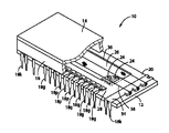
FIG. 1 is a perspective view showing an entire configuration of a
[0020]
One
[0021]
At a position on the
[0022]
At both ends of the
[0023]
FIG. 2A is a plan view showing the entire
[0024]
As shown in an enlarged view of a portion b in FIG. 2B, the
[0025]
In FIG. 2B, a conductor material (conductor layer 52) is fixed to a portion where a substantial portion of the
[0026]
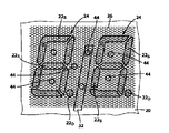
FIG. 3 shows an example of the
[0027]
FIG. 4 is a diagram for explaining the main configuration of the
[0028]
The
[0029]
On the
[0030]
A part of the
[0031]
FIG. 5 shows the support structure of the
[0032]
As shown in FIG. 4, the
[0033]
Further, as is clear from the relationship between the size of the openings of the
[0034]
When driving the
[0035]
At this time, in the present embodiment, each of the conductor layers 50 laminated for each of the plurality of regions of the
[0036]
Further, in the present embodiment, although the mutual distance between the
[0037]
Further, in the present embodiment, since the
[0038]
Further, in the present embodiment, when the
[0039]
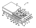
Incidentally, in the conventional
[0040]
Incidentally, the above-mentioned
[0041]
Subsequently, in a
[0042]
In the sealing step 72, for example, a lead frame, a
[0043]
In the above manufacturing process, the
[0044]
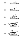
In the first
[0045]
Next, in a spherical
[0046]
After the above-described steps, the organic paste and the solvent are removed by performing drying and baking under predetermined conditions according to the composition of the
[0047]
Therefore, according to the present embodiment, the plurality of
[0048]
Moreover, since the positions of the plurality of
[0049]
Incidentally, in the conventional
[0050]
Further, according to the present embodiment, as described above, a plurality of
[0051]
FIG. 10 is a diagram showing a main part of a
[0052]
Below the
[0053]
Therefore, according to the present embodiment, since the shading by the
[0054]
In the above-described embodiment, the
[0055]
That is, first, a release layer is formed on a substrate having predetermined heat resistance. The release layer is made of a high melting point particle such as alumina or glass having an average particle diameter of about 0.01 to 5 (μm) which is not sintered at a firing temperature described later, and a resin such as ethyl cellulose. It is provided with a thickness of about 50 (μm) or less by using a thick film screen printing method or the like. Next, after performing a drying process on this, a thick film dielectric paste is repeatedly applied thereon in a shape corresponding to the plane shape of the
[0056]
Then, on a lattice-shaped dielectric resin film formed of the above-mentioned thick-film dielectric paste, a thick-film conductor paste in which a conductive powder such as carbon or silver and a glass frit are dispersed in an organic solvent together with a resin, for example, It is applied in the shape of the
[0057]
After laminating the dielectric resin film and the conductor resin film as described above, drying and removing the solvent, and performing a firing treatment at a temperature sufficiently higher than the softening point of the glass frit contained therein, the dielectric The body resin film and the conductor resin film are sintered to form the
[0058]
As described above, the present invention has been described in detail with reference to the drawings. However, the present invention can be implemented in other embodiments.
[0059]
For example, in the embodiment, the
[0060]
Further, in the embodiment, the case where one
[0061]
Also, since there is no particular problem with the
[0062]
Further, in the embodiment, the case where the
[0063]
Further, in the embodiment, the
[0064]
Further, in the
[0065]
In the case of increasing the aperture ratio as described above, in addition to dropping one of the warp and the weft constituting the lattice as shown in the examples, the interval between the warp and the weft is increased together or only one of them. The aperture ratio can be increased by an appropriate method.
[0066]
In the embodiment, the
[0067]
In the embodiment, the
[0068]
Further, in the
[0069]
In the embodiment, the
[0070]
Although not specifically exemplified, the present invention can be variously modified without departing from the gist thereof.
[Brief description of the drawings]
FIG. 1 is a perspective view showing a whole of a fluorescent display tube according to an embodiment of the present invention, with a part thereof being cut away.
2A is a plan view showing the entire grid electrode member provided in the fluorescent display tube of FIG. 1, and FIG. 2B is an enlarged view of a portion b of FIG.
FIG. 3 is an enlarged view illustrating a main part of a display surface of the fluorescent display tube of FIG. 1;
FIG. 4 is a diagram illustrating a cross-sectional structure of the fluorescent display tube of FIG.
FIG. 5 is a diagram illustrating in detail a fixing structure of a grid electrode member.
FIG. 6 is a perspective view showing an entire fluorescent display tube provided with a conventional grid electrode.
FIG. 7 is a process diagram illustrating a process of manufacturing the fluorescent display tube of FIG.
8 is a process diagram illustrating a mesh fixing process in the manufacturing process of FIG. 7;
9 (a) to 9 (e) are schematic diagrams showing the state of a spherical spacer arrangement portion at each stage of the process of FIG. 8;
FIG. 10 is a diagram illustrating an arrangement of grid electrodes according to another embodiment of the present invention.
[Explanation of symbols]
10: fluorescent display tube
12: Substrate
20: Display surface
22: phosphor layer
26: Grid electrode member (control electrode member)
26a: grid electrode (control electrode)
44: spherical spacer (point-like support)
46, 48: conductive adhesive layer
50: mesh (mesh-like member)
Claims (5)
前記蛍光体層および前記陰極の間の高さ位置に配置された絶縁体材料製の平坦な網目状部材と、
前記発光区分単位で相互に所定距離隔てて前記網目状部材上に区画された複数の領域毎にその網目状部材に積層された前記制御電極として機能させられる複数の導体層と
を、含むことを特徴とする蛍光表示管。A plurality of phosphor layers provided in a predetermined shape on the display surface of the substrate; a cathode provided above the phosphor layer; and a plurality of the phosphor layers located at a height between the plurality of phosphor layers and the cathode. A plurality of control electrodes that cover each of the body layers for each predetermined light-emitting section, and control the electrons generated from the cathode with the control electrodes to make the phosphor layers incident on the phosphor layers. A fluorescent display tube of a type that selectively emits light,
A flat mesh member made of an insulator material disposed at a height position between the phosphor layer and the cathode,
A plurality of conductor layers that function as the control electrodes stacked on the mesh member for each of a plurality of regions partitioned on the mesh member at a predetermined distance from each other in the light emitting section unit. Characteristic fluorescent display tube.
絶縁体材料製の平坦な網目状部材と、その網目状部材上に区画された複数の領域毎に相互に所定距離隔ててその網目状部材に積層された前記制御電極として機能させられる複数の導体層とを含むことを特徴とする蛍光表示管の制御電極部材。A control electrode member disposed on a display surface of a fluorescent display tube so as to cover the plurality of phosphor layers in order to provide a plurality of control electrodes for controlling electrons directed to the plurality of phosphor layers for each predetermined light emitting section. And
A flat mesh member made of an insulator material, and a plurality of conductors functioning as the control electrodes stacked on the mesh member at a predetermined distance from each other in a plurality of regions partitioned on the mesh member And a control electrode member of the fluorescent display tube.
Priority Applications (1)
| Application Number | Priority Date | Filing Date | Title |
|---|---|---|---|
| JP2002163476A JP2004014200A (en) | 2002-06-04 | 2002-06-04 | Fluorescent display tube, and control electrode member of the same |
Applications Claiming Priority (1)
| Application Number | Priority Date | Filing Date | Title |
|---|---|---|---|
| JP2002163476A JP2004014200A (en) | 2002-06-04 | 2002-06-04 | Fluorescent display tube, and control electrode member of the same |
Publications (1)
| Publication Number | Publication Date |
|---|---|
| JP2004014200A true JP2004014200A (en) | 2004-01-15 |
Family
ID=30431952
Family Applications (1)
| Application Number | Title | Priority Date | Filing Date |
|---|---|---|---|
| JP2002163476A Pending JP2004014200A (en) | 2002-06-04 | 2002-06-04 | Fluorescent display tube, and control electrode member of the same |
Country Status (1)
| Country | Link |
|---|---|
| JP (1) | JP2004014200A (en) |
Cited By (1)
| Publication number | Priority date | Publication date | Assignee | Title |
|---|---|---|---|---|
| JP2009176568A (en) * | 2008-01-24 | 2009-08-06 | Nippon Hoso Kyokai <Nhk> | Display device |
-
2002
- 2002-06-04 JP JP2002163476A patent/JP2004014200A/en active Pending
Cited By (1)
| Publication number | Priority date | Publication date | Assignee | Title |
|---|---|---|---|---|
| JP2009176568A (en) * | 2008-01-24 | 2009-08-06 | Nippon Hoso Kyokai <Nhk> | Display device |
Similar Documents
| Publication | Publication Date | Title |
|---|---|---|
| KR100767904B1 (en) | Image display apparatus | |
| US20060246295A1 (en) | Thick-film sheet member, devices to which the sheet member is applied, and methods of producing the sheet member and the devices | |
| JP3839713B2 (en) | Method for manufacturing flat display | |
| JP2002075255A (en) | Fluorescent display tube | |
| JP2004014200A (en) | Fluorescent display tube, and control electrode member of the same | |
| US7132784B2 (en) | Fluorescent display tube having provision for preventing short-circuit therein, and method of manufacturing the same | |
| JP2883014B2 (en) | Fluorescent display tube | |
| JP2002367542A (en) | Field emission display and method of manufacturing the same | |
| JP3418319B2 (en) | Fluorescent display tube | |
| JP2544068Y2 (en) | Fluorescent display | |
| JP2899331B2 (en) | Fluorescent light emitting device | |
| JP3018292U (en) | Fluorescent display tube | |
| RU2258974C1 (en) | Low-voltage cathode-ray fluorescent matrix screen | |
| JP2000353483A (en) | Anode substrate for fluorescent character display tube | |
| JPH0622922Y2 (en) | Fluorescent tube | |
| JP3563316B2 (en) | Method for manufacturing anode substrate of rib grid type fluorescent display tube | |
| JPH0635360Y2 (en) | Fluorescent display tube | |
| JP2528456Y2 (en) | Fluorescent display | |
| JP2004206977A (en) | Conductor alignment method and thick film sheet member | |
| JP2005093125A (en) | Image display device and its manufacturing method | |
| JPS603487Y2 (en) | Fluorescent display tube substrate device | |
| KR940009192B1 (en) | Manufacturing method of display pattern for fluorescent display | |
| JP2003208862A (en) | Fluorescent display tube and manufacturing method thereof | |
| JPH0245962Y2 (en) | ||
| JPH023251B2 (en) |