JP2004007575A - High frequency device, and communication apparatus - Google Patents
High frequency device, and communication apparatus Download PDFInfo
- Publication number
- JP2004007575A JP2004007575A JP2003108328A JP2003108328A JP2004007575A JP 2004007575 A JP2004007575 A JP 2004007575A JP 2003108328 A JP2003108328 A JP 2003108328A JP 2003108328 A JP2003108328 A JP 2003108328A JP 2004007575 A JP2004007575 A JP 2004007575A
- Authority
- JP
- Japan
- Prior art keywords
- electrode
- balanced
- terminal
- frequency device
- pair
- Prior art date
- Legal status (The legal status is an assumption and is not a legal conclusion. Google has not performed a legal analysis and makes no representation as to the accuracy of the status listed.)
- Pending
Links
Images


Abstract
Description
【0001】
【発明の属する技術分野】
本発明は、たとえば携帯電話などに用いられる、例えば弾性表面波フィルタ及び複合電子部品として実現される高周波デバイス等に関するものである。
【0002】
【従来の技術】
近年、移動体通信の発展に伴い、使用される部品の高性能化、小型化が期待されている。さらに、対雑音特性の良好化を目的としてICなどの半導体部品の平衡化が進み、RF段に使用されるフィルタにおいても平衡化が求められている。従来、移動体通信機器などのRF段のフィルタとしては、弾性表面波フィルタが広く用いられている。特に、縦モード型の弾性表面波フィルタはインターディジタルトランスデューサ電極の構成上、平衡−不平衡変換が容易に実現でき、平衡型入出力端子を有するRF段のフィルタとして、低ロス、高減衰、良好なバランス特性が期待されている。
【0003】
以下、従来の平衡型入出力端子を有する縦モード型の弾性表面波フィルタについて説明する。
【0004】
図9(a)に従来の平衡型入出力端子を有する縦モード型の弾性表面波フィルタの構成を示す(例えば、特許文献1を参照)。図9(a)において、弾性表面波フィルタ901は、圧電基板911上に、それぞれ一対の電極指から構成された第1、第2、第3のインターディジタルトランスデューサ電極(以下、IDT電極とする)902、903、904と第1、第2の反射器電極905、906とにより構成される。第1のIDT電極902の一方の電極指902aは不平衡型入出力端子909に接続され、第1のIDT電極902の他方の電極指902bは接地されている。また、第2のIDT電極903の一方の電極指903aは平衡型入出力端子の一方の第1の端子907に接続され、他方の電極指903bは接地されている。また、第3のIDT電極904の一方の側の電極指904aは平衡型入出力端子の他方の第2の端子908に接続され、他方の電極指904bは接地されている。
【0005】
以上の構成とすることにより、不平衡型−平衡型入出力端子を有する弾性表面波フィルタが得られる。なお、実際には、不平衡型入出力端子909,平衡型入出力端子907,908は、IDT電極902〜904と同一の圧電基板上に形成されるが、ここでは模式的に圧電基板911の外にあるものとして示した。
【0006】
また、図9(b)において弾性表面波フィルタ901の、平衡型入出力端子の第1、第2の端子907、908間には、インピーダンス整合用として第1のインダクタ910が接続されている。この構成にすることにより、平衡型入出力端子の第1、第2の端子907、908間のインピーダンス整合を行っている。
【0007】
このようなフィルタに関しては、良好なバランス特性を得るために、弾性表面波フィルタを構成する各IDT電極902〜903、および第1,第2の反射器電極905,906の設計およびレイアウトは、不平衡型入出力端子909が接続された電極指902aからみて、対称に近づくように施工されている。
【0008】
図10に示すのは、図9に示した従来の弾性表面波フィルタの特性図である。ただし、1800MHz帯で動作するものを例に示した。図10において、(a)は通過特性であり、(b)は通過帯域(1805MHzから1880MHzまで)における振幅バランス特性、(c)は通過帯域における位相バランス特性をそれぞれ示している。ここで、振幅バランス特性とは、平衡型入出力端子の一方の第1の端子907と不平衡型入出力端子909との信号振幅と平衡型入出力端子の他方の第2の端子908と不平衡型入出力端子909との信号振幅との振幅差を表したものであり、この値が零となればバランス特性の劣化はない。
【0009】
また、位相バランス特性とは、平衡型入出力端子の一方の第1の端子907と不平衡型入出力端子909との信号の位相と平衡型入出力端子の他方の第2の端子908と不平衡型入出力端子909との信号の位相との位相差の180度からのずれを表したものであり、この値が零となればバランス特性の劣化はない。
【0010】
今回、図10(b)、(c)に示したバランス特性は、第2の端子908から第1の端子907を見た場合である。ここで、逆に見た場合は両特性とも上下反転した波形となる。
【0011】
【特許文献1】
特開平6−204781号公報
【0012】
【発明が解決しようとする課題】
しかしながら、上述の弾性表面波フィルタにおいては、対称構造であるにも関わらず、図10より、通過帯域において、振幅バランス特性は−0.3dB〜+1.4dB、位相バランス特性は−14°〜−1°であり、重要な電気的特性の一つであるバランス特性の劣化が大きいという課題があった。
【0013】
これはバランス特性の劣化が構造だけではなく、寄生成分による入出力のIDT電極間の結合に起因するものである。
【0014】
例えば、図9の弾性表面波フィルタ901においては、不平衡型入出力端子909から見て、平衡型入出力端子の第1の端子907までの距離にある電極指の本数と、平衡型入出力端子の第2の端子908までの距離にある電極指の本数とは異なっている。このため電極指間の寄生成分の総和も異なり、これがIDT電極間の結合をアンバランスなものとする。
【0015】
例えば800MHz〜900MHz帯のような周波数帯域においては、このバランス特性の劣化は現れにくいが、システムが高周波数に対応すると、上述した1800MHzのような高周波領域でも信号の送受信が用いられる。したがって、フィルタが扱う周波数が高くなるにつれてこの影響は無視できなくなり、これを考慮した設計が必要となる。
【0016】
しかしながら、例えば不平衡型入出力端子909から見て、平衡型入出力端子の第1の端子907までの距離にある電極指の本数と、平衡型入出力端子の第2の端子908までの距離にある電極指の本数とを同数となるように設計しても、IDT電極902〜904の形状は、理想的に対称とすることはできないため、IDT電極間の結合をバランス化することはできない。
【0017】
さらに、バランス特性の劣化は、平衡型のフィルタにおいては、弾性表面波フィルタばかりでなく、レイアウトを対称に設計することが容易なはずの、円筒形のフィルタ、誘電体フィルタ等のフィルタでも生じることがあり、有効な解決が求められていた。
【0018】
本発明では、上記の課題に鑑みてなされたものであり、平衡型の入出力端子を有する高周波帯で動作する高周波素子を内蔵した高周波デバイスに関して、良好なバランス特性を有する高周波デバイス、およびそれを用いた通信機器を得ることを目的とするものである。
【0019】
【課題を解決するための手段】
上記の目的を達成するために、第1の本発明は、平衡型の一対の端子を少なくとも一つ有する高周波素子と、
前記高周波素子の端子と接続された外部入出力端子とを備え、
前記平衡型の一対の端子と、その平衡型の一対の端子にそれぞれ接続された前記外部入出力端子との間の各インピーダンス値は互いに異なる高周波デバイスである。
【0020】
また、第2の本発明は、前記各インピーダンス値の異なりは、前記高周波素子の前記平衡型の一対の端子のうち、他方に対して相対的に位相が進んでいる一方の端子の方が大きい第1の本発明の高周波デバイスである。
【0021】
また、第3の本発明は、前記平衡型の一対の端子の少なくとも一方と、その平衡型の一対の端子の前記一方に接続された前記外部入出力端子との間に設けられた第1のリアクタンス素子を備えた第2の本発明の高周波デバイスである。
【0022】
また、第4の本発明は、前記平衡型の一対の端子の他方と、その平衡型の一対の端子の前記他方に接続された前記外部入出力端子との間に設けられた、前記第1のリアクタンス素子とインピーダンス値が異なる第2のリアクタンス素子をさらに備えた第3の本発明の高周波デバイスである。
【0023】
また、第5の本発明は、前記第1のリアクタンス素子および/または第2のリアクタンス素子は、前記高周波素子を前記高周波デバイス内にワイヤーボンディング実装を行う際のワイヤーのインダクタンス成分として実現されている第3または第4の本発明の高周波デバイスである。
【0024】
また、第6の本発明は、前記第1のリアクタンス素子と前記第2のリアクタンス素子のインピーダンス値の差を終端インピーダンスで規格化した値が0.2以下である第4の本発明の高周波デバイスである。
【0025】
また、第7の本発明は、一方の主面上に設けられた表層電極と、その内層に設けられた少なくとも1層以上の内層電極と、前記表層電極と前記内層電極とを接続するビアホール電極とを有する積層基板を備え、
前記外部入出力端子は、前記表層電極として実現され、
前記高周波素子は、前記基板の他方の主面上に実装され、
前記第1のリアクタンス素子および/または第2のリアクタンス素子は、前記内層電極によるインダクタンス成分で実現されている第3または第4の本発明の高周波デバイスである。
【0026】
また、第8の本発明は、前記平衡型の一対の端子の少なくとも一方と、その平衡型の一対の端子の前記一方に接続された前記外部入出力端子との間にその一端が接続され、他端が接地された第1のサセプタンス素子を備えた第2の本発明の高周波デバイスである。
【0027】
また、第9の本発明は、前記平衡型の一対の端子の他方と、その平衡型の一対の端子の前記他方に接続された前記外部入出力端子との間にその一端が接続され、他端が接地された、前記第1のサセプタンス素子とアドミッタンス値が異なる第2のサセプタンス素子を備えた第8の本発明の高周波デバイスである。
【0028】
また、第10の本発明は、前記第1のサセプタンス素子と前記第2のサセプタンスのアドミッタンス値の差を終端インピーダンスで規格化した値が5以上である第9の本発明の高周波デバイスである。
【0029】
また、第11の本発明は、積層した複数の誘電体層と、
前記誘電体層間に設けられた層間電極と、
前記層間電極の全部または一部を接続する、複数の前記誘電体層にまたがって設けられたビアホール導体とを備え、
前記層間電極および前記ビアホール導体は、複数のストリップラインおよび複数のコンデンサを形成し、
前記第1のリアクタンス素子および第2のリアクタンス素子は、前記複数のストリップライン、前記複数のコンデンサおよび前記ビアホール導体により構成されている第4の本発明の高周波デバイスである。
【0030】
また、第12の本発明は、積層した複数の誘電体層と、
前記誘電体層間に設けられた層間電極と、
前記層間電極の全部または一部を接続する、複数の前記誘電体層にまたがって設けられたビアホール導体とを備え、
前記層間電極および前記ビアホール導体は、複数のストリップラインおよび複数のコンデンサを形成し、
前記第1のサセプタンス素子および第2のサセプタンス素子は、前記複数のストリップライン、前記複数のコンデンサおよび前記ビアホール導体により構成されている第4の本発明の高周波デバイスである。
【0031】
また、第13の本発明は、前記高周波素子は、高周波フィルタである第1の本発明の高周波デバイスである。
【0032】
また、第14の本発明は、前記高周波フィルタは、
圧電基板と、
前記圧電基板上に設けられた、少なくとも一つのインターディジタルトランスデューサ電極とを備えた弾性表面波フィルタである第13の本発明の高周波デバイスである。
【0033】
また、第15の本発明は、前記圧電基板上に形成された、前記平衡型の一対の端子のそれぞれと前記インターディジタルトランスデューサ電極との間に設けられた第1および第2の引き回し電極を備え、
前記第1および第2の引き回し電極の形状又は長さが異なる第14の本発明の高周波デバイスである。
【0034】
また、第16の本発明は、前記インターディジタルトランスデューサ電極は、少なくとも第1、第2および第3の3つのインターディジタルトランスデューサ電極から構成され、
前記弾性表面波フィルタは、少なくとも2つの前記インターディジタルトランスデューサ電極を用いた平衡型の弾性表面波フィルタであって、
前記第1のインターディジタルトランスデューサ電極の一方の電極指は不平衡型の入出力端子に接続され、他方の電極指は接地され、
前記第2のインターディジタルトランスデューサ電極の一方の電極指は前記平衡型の一対の端子の一方の第1の端子に接続されると共に、他方の電極指は接地され、
前記第3のインターディジタルトランスデューサ電極の一方の電極指は前記平衡型の一対の端子の他方の第2の端子に接続されると共に、他方の電極指は接地されている第14の本発明の高周波デバイスである。
【0035】
また、第17の本発明は、前記インターディジタルトランスデューサ電極は、少なくとも第1、第2および第3の3つのインターディジタルトランスデューサ電極から構成され、
前記弾性表面波フィルタは、少なくとも2つの前記インターディジタルトランスデューサ電極を用いた平衡型の弾性表面波フィルタであって、
前記第1のインターディジタルトランスデューサ電極の一方の電極指は前記平衡型の一対の端子の一方の第1の端子に接続されると共に、他方の電極指は前記平衡型の一対の端子の他方の第2の端子に接続され、
前記第2および前記第3のインターディジタルトランスデューサ電極の一方の電極指は、共通の不平衡型の入出力端子に接続されると共に、他方は接地されている第14の本発明の高周波デバイスである。
【0036】
また、第18の本発明は、前記第2の電極指の一方と前記第1の端子との間に接続された第1の共振器と、
前記第3の電極指の一方と前記第2の端子に接続された第2の共振器とを備えた第16または第17の本発明の高周波デバイスである。
【0037】
また、第19の本発明は、前記第1の共振器および前記第2の共振器の形状は互いに異なる第18の本発明の高周波デバイスである。
【0038】
また、第20の本発明は、前記平衡型の一対の端子の一方と、前記平衡型の端子の他方とを接続するインダクタを備えた第1の本発明の高周波デバイスである。
【0039】
また、第21の本発明は、送信手段および/または受信手段を備え、
前記送信手段または前記受信手段は、第1から第20のいずれかの本発明の高周波デバイスを用いた通信機器である。
【0040】
なお、前記インダクタが、前記積層体表層に部品として実装されていてもよい。
【0041】
また、前記インダクタが、前記積層体内層に構成された前記複数のストリップライン及び前記ビアホール導体により構成されていてもよい。
【0042】
【発明の実施の形態】
以下では、本発明にかかる実施の形態について、図面を参照しつつ説明を行う。
【0043】
(実施の形態1)
はじめに、図1(a)を参照しながら、本発明の実施の形態1の平衡型フィルタデバイスについて説明する。なお、図1(a)は、本実施の形態における平衡型入出力端子を有する弾性表面波フィルタの構成を示し、図1(b)は、図1(a)の弾性表面波フィルタを備えた平衡型フィルタデバイスの構成を示す。
【0044】
図1(a)において、本実施の形態の弾性表面波フィルタ101は、圧電基板117上に、それぞれ一対の電極指から構成された第1、第2、第3のIDT電極102、103、104と第1、第2の反射器電極105、106、第1、第2の弾性表面波共振器107、108とにより構成されている。
【0045】
ここで、第1,第2の弾性表面波共振器107,108は、フィルタ特性に減衰特性を持たせる為、及び整合を取る為等に用いており、その形状は、第1及び第2の弾性表面波共振器107,108で同一である。
【0046】
第1のIDT電極102の一方の電極指102aは不平衡型入出力端子109に接続され、他方の電極指102bは接地されている。また、第2のIDT電極103の一方の電極指103aは第1の弾性表面波共振器107に接続され、他方の電極指103bは接地されている。また、第3のIDT電極104の一方の電極指104aは第2の弾性表面波共振器108に接続され、他方の電極指104bは接地されている。
【0047】
更に、第1の弾性表面波共振器107は平衡型入出力端子の一方の第1の端子110に接続され、第2の弾性表面波共振器108は平衡型入出力端子の他方の第2の端子111に接続されている。以上の構成とすることにより不平衡型−平衡型入出力端子を有する弾性表面波フィルタが得られる。なお、この構成は、第1,第2の弾性表面波共振器107,108を備えたことを除けば、図9(a)に示す従来の弾性表面波フィルタ901と同様である。また、実際には、不平衡型入出力端子109,平衡型入出力端子の第1,第2の端子110,111は、IDT電極102〜103と同一の圧電基板上に形成されるが、ここでは模式的に圧電基板117の外にあるものとして示した。これは以下に説明する各弾性表面波フィルタの図においても同様である。
【0048】
また、図1(b)に示す平衡型フィルタデバイス120において、弾性表面波フィルタ101の不平衡型入出力端子109は第1の入出力端子113に接続されている。
【0049】
また、平衡型入出力端子の一方の第1の端子110と第2の入出力端子114の間にリアクタンス素子として第2のインダクタ116が接続され、平衡型入出力端子の他方の第2の端子111は第3の入出力端子115に接続されている。
【0050】
さらに、平衡型入出力端子の第1の端子110と第2のインダクタ116との間の接続点121と、第2の端子111と第3の入出力端子115との間の接続点121には、インピーダンス整合用として第1のインダクタ112が接続されている。
【0051】
図2に示すのは図1(b)に示した平衡型フィルタデバイス120の具体的な特性である。図2において、(a)は通過特性であり、(b)は通過帯域における振幅バランス特性、(c)は通過帯域における位相バランス特性である。図2より、リアクタンス素子として第2のインダクタ116を平衡型入出力端子の一方の第1の端子110に接続することにより、通過帯域において、振幅バランス特性は−0.7dB〜+1.5dB、位相バランス特性は−7.1°〜+4.4°を得ている。このように、図10の弾性表面波フィルタの特性に比べて、通過特性、振幅バランス特性をほとんど劣化させることなく、位相バランス特性が改善することが可能となる。なお、図2(b)の振幅バランス特性は誇張して描かれており、実際はほとんど劣化しない。
【0052】
ここで、図2(b)、(c)に示したバランス特性は、第3の入出力端子115から第2の入出力端子114を見た場合の特性を示している。具体的には、図2(c)において、位相バランス特性が0°からマイナス側に劣化している、すなわち平衡型入出力端子の第1の端子110側の位相が進んでいるため、基準とした第3の入出力端子115側ではなく、第2の入出力端子114側に第2のインダクタ116を接続することにより、位相バランス特性が改善されている。
【0053】
ここで、今回接続した第2のインダクタ116のインピーダンスは実質上13.5Ωであり、終端インピーダンスで規格化した場合の値は0.18である。
【0054】
なお、本実施の形態では、従来の特性がマイナス側に劣化している場合を例としたが、従来の特性がプラス側に劣化している場合は、基準とした第3の入出力端子115側にインダクタを接続することにより位相バランス特性を改善することが同様に可能となる。すなわち、弾性表面波フィルタ101単体で位相バランス特性を測定したときに、平衡型入出力端子の第1,第2の端子110,111のいずれかからみて、位相が進んでいると認められた場合の端子と、その端子が接続された第2の入出力端子114または第3の入出力端子115との間に、第2のインダクタ116を設けるようにする。つまり、平衡型入出力端子の第1,第2の端子110,111のうち、相対的に位相が進んでいるほうのインピーダンスを大きくする。
【0055】
なお、本実施の形態では、第2のインダクタ116の終端インピーダンスで規格化した値が0.18の場合を例としたが、この値が0.2以下であれば同様の効果が得られる。
【0056】
なお、本実施の形態では、弾性表面波フィルタの構成として図1(a)について説明したが、図3の弾性表面波フィルタ301として示すように、図1(a)の第1、第2の弾性表面波共振器107,108がない場合(これは図9に示す従来の弾性表面波フィルタと同等の構成となる)の構成であってもよい。
【0057】
或いは図4の弾性表面波フィルタ401に示すように、圧電基板410上に、それぞれ一対の電極指から構成される第1、第2、第3のIDT電極402、403、404と第1、第2の反射器電極405、406とにより構成され、第1のIDT電極402の一方の電極指402aは平衡型入出力端子の一方の第1の端子407に接続され、第1のIDT電極402の他方の電極指402bは平衡型入出力端子の他方の第2の端子408に接続され、更に、第2、第3のIDT電極403、404の一方の電極指403aおよび404aを不平衡型入出力端子409に接続し、他方の電極指403bおよび404bを接地するような構成を用いても同様の効果が得られる。
【0058】
すなわち、本実施の形態の平衡型フィルタデバイス120は、内蔵する弾性表面波フィルタが従来例と同じく位相バランス特性が劣化していても、フィルタの外部でインダクタを接続することにより、インピーダンス値を平衡型入出力端子の第1の端子110と第2の端子111とで異ならせて、これを改善することができる。通信装置等において、他の回路とともに組み込まれる場合は、平衡型フィルタデバイス120として実装されるため、位相バランス特性に優れた弾性表面波フィルタが容易に得られることになる。
【0059】
なお、本実施の形態では、第1のインダクタ112を平衡型入出力端子の一方の第1の端子110と平衡型入出力端子の他方の第2の端子111の間に接続しているが、第1のインダクタ112無しでインピーダンス整合が取れる場合は、第1のインダクタ112を接続する必要はなく、これを省略した構成としても良い。
【0060】
(実施の形態2)
図5を参照しながら、本発明の実施の形態2の高周波フィルタデバイスについて説明する。なお、図5は、本実施の形態における平衡型入出力端子を有する高周波フィルタデバイスの構成を示している。
【0061】
図5において、本実施の形態の平衡型フィルタデバイスは、図1(a)で示したような弾性表面波フィルタ101と同等のIDT電極、反射器電極や弾性表面波共振器等から構成されている弾性表面波フィルタ500を備えている。第1の入出力端子501は、弾性表面波フィルタ500の不平衡型入出力端子511(図1の不平衡型入出力端子109に相当する)に接続され、平衡型入出力端子の一方の第1の端子504と平衡型入出力端子の他方の第2の端子505の間にはインピーダンス整合用として第1のインダクタ506が接続されている。
【0062】
更に、平衡型入出力端子の一方の第1の端子504と第2の入出力端子502の間にリアクタンス素子として第2のインダクタ507が接続され、平衡型入出力端子の他方の第2の端子505と第3の入出力端子503の間にリアクタンス素子として第3のインダクタ508が接続されている。
【0063】
ここで、図1(a)の平衡型入出力端子の一方の第1の端子110は図5の平衡型入出力端子の一方の第1の端子504に対応しており、図1(a)の平衡型入出力端子の他方の第2の端子111は図5の平衡型入出力端子の他方の第2の端子505に対応している。ここで、第2のインダクタ507と第3のインダクタ508の値の関係として、インダクタ値の差を本実施の形態1に示した第2のインダクタ116と同値になるように設定することにより、図2(a)〜(c)に示した特性と同等の特性が得られる。要するに、弾性表面波フィルタ500単体で位相バランス特性を測定したときに、平衡型入出力端子の第1,第2の端子504,505のいずれかからみて、位相が進んでいると認められた側の端子と接続されたインダクタ(第2のインダクタ507または第3のインダクタ508)のインダクタ値の値を大きくなるように設定する。
【0064】
これに対して、第2のインダクタ507と第3のインダクタ508を同値になるようにすると、図10で示した従来特性と同等の特性となり、バランス特性の劣化が改善されることは無い。
【0065】
すなわち、平衡型入出力端子の第1、第2の端子504、505それぞれに異なるリアクタンス成分を接続することにより、図10の弾性表面波フィルタの特性に比べて、通過特性、振幅バランス特性をほとんど劣化させることなく、位相バランス特性が改善することが可能となる。
【0066】
具体的には、図10(c)において、位相バランス特性が0°からマイナス側に劣化しているため、第2の入出力端子502側に対して、第3の入出力端子503側に接続された第3のインダクタ508よりインピーダンスの大きい第2のインダクタ507を接続することにより、位相バランス特性が改善されている。ここで、今回接続した第2のインダクタ507と第3のインダクタ508のインピーダンスの差は実質上13.5Ωであり、終端インピーダンスで規格化した場合の値は0.18である。
【0067】
なお、本実施の形態では、従来の特性がマイナス側に劣化している場合を例としたが、従来の特性がプラス側に劣化している場合は、基準とした第3の入出力端子503側の第3のインダクタ508のインピーダンス値を第2の入出力端子502側の第2のインダクタ507より大きくすることにより位相バランス特性を改善することが同様に可能となる。つまり、平衡型入出力端子の第1,第2の端子504,505のうち、相対的に位相が進んでいるほうのインピーダンスを大きくする。
【0068】
なお、本実施の形態では、第2のインダクタ507と第3のインダクタ508の終端インピーダンスで規格化した値の差が0.18の場合を例としたが、この値が0.2以下であれば同様の効果が得られる。
【0069】
なお、本実施の形態では、弾性表面波フィルタの構成として、図1(a)と同一の場合について説明したが、図3,4に示すような構成の弾性表面波フィルタの構成を用いても同様の効果が得られる。
【0070】
なお、本実施の形態では、第1のインダクタ506を平衡型入出力端子の一方の第1の端子504と平衡型入出力端子の他方の第2の端子505の間に接続しているが、第1のインダクタ506無しでインピーダンス整合が取れる場合は、第1のインダクタ506を接続する必要はない。
【0071】
(実施の形態3)
次に図6を参照しながら、本発明の実施の形態3の平衡型フィルタデバイスの具体的な構造について説明する。
【0072】
図6において、本実施の形態の平衡型フィルタデバイス620は、圧電基板600上に構成された弾性表面波フィルタを有し、この弾性表面波フィルタが、セラミックなどを主材料としたパッケージ基板606にワイヤーボンディング実装を用いて、実装された構成を有している。また、圧電基板600上に不平衡型入出力端子電極601、平衡型入出力端子の一方の第1の端子電極602、平衡型入出力端子電極の他方の第2の端子電極603及び接地電極604、605が形成されている。
【0073】
更に、パッケージ基板606上に第1〜第5の電極607〜611が形成されている。不平衡型入出力端子電極601は第1のワイヤー612を介して第1の電極607に接続され、平衡型入出力端子の一方の第1の端子電極602は第2のワイヤー613を介して第2の電極608に接続され、平衡型入出力端子の他方の第2の端子電極603は第3のワイヤー614を介して第3の電極609に接続されている。また、接地電極604、605は第4、第5のワイヤー615、616を介して、それぞれ第4、第5の電極610、611に接続されている。
【0074】
ここで、平衡型入出力端子の一方の第1の端子電極602に接続された第2のワイヤー613と平衡型入出力端子の他方の第2の端子電極603に接続された第3のワイヤー614の長さは、異なるインピーダンスを持たせるため、非対称に構成されている。
【0075】
従って、パッケージ基板606への実装の際に、圧電基板600の方向性を変更し、平衡型入出力端子の第1、第2の端子電極602、603それぞれに接続されるワイヤーの長さを非対称に構成することにより、図5に示す構成と同等になり、図2(b)に示したような位相バランス特性を改善した特性を得ることが可能となる。
【0076】
なお、本実施の形態では、ワイヤーを用いてリアクタンス成分を形成しているが、圧電基板上での引き回し電極を用いてリアクタンス成分を形成しても同様の効果が得られる。このときに限り、第2のワイヤー613と第3のワイヤー614とは対称の長さとしてもよい。もちろん違えていても良い。
【0077】
また、図1で示した第1の弾性表面波共振器107及び第2の弾性表面波共振器108の形状を異ならしめることによっても、平衡型入出力端子の負荷のインピーダンスを変えることができ、そのため同様に位相バランス特性を改善した特性を得ることが可能となる。
【0078】
(実施の形態4)
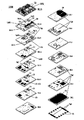
図7及び図8を参照しながら、本発明の実施の形態4の平衡型フィルタデバイスについて説明する。なお、図7は、本実施の形態における平衡型フィルタデバイスの構造の断面図を、図8は構造の分解斜視図を示している。
【0079】
図7において、平衡型フィルタデバイス710は、圧電基板700上に構成された、図1、図3,図4と同様の構成を有する弾性表面波フィルタが、複数の誘電体層を積層した積層体701上に、フリップチップ実装を用いて実装された構成を有している。弾性表面波フィルタの不平衡型入出力端子、平衡型入出力端子などは金などを主成分とするバンプ702を介して、積層体701上の電極703と電気的に接続される。ただし図においては平衡型入出力端子のみを示すものとした。
【0080】
更に、電極703は積層体701の内層に構成されたビアホール電極704、内部電極705を介して、積層体701の底面に形成された端子電極706と電気的に接続され、端子電極706はメイン基板(図示せず)と電気的に接続される。
【0081】
図7の具体的な構成として図8に分解斜視図を示す。積層体701は3層の誘電体層701a〜701cから構成されている。なお、誘電体層の積層枚数は適宜に選択されるものである。
【0082】
第1の誘電体層701a上には電極703a〜703dが形成され、第2の誘電体層701b上には内部電極705aが形成され、第3の誘電体層701c上には内部電極705b、705cが形成されている。また、第3の誘電体層701cの裏面には、メイン基板(図示せず)と接続するための端子電極706a〜706dが形成されており、電極703a〜703d、内部電極705a〜705c及び端子電極706a〜706dを電気的に接続するためにビアホール電極704a〜704gが適宜配置されている。
【0083】
圧電基板700上に形成された弾性表面波フィルタの不平衡型入出力端子は電極703aにバンプ等を介して電気的に接続される。また、平衡型入出力端子の一対の入出力端子はそれぞれ電極703b、703cに、接地端子は電極703dにバンプなどを介して電気的に接続される。
【0084】
電極703aはビアホール電極704aを介して第3の誘電体層701cに形成された内部電極705cに接続され、更にビアホール電極704bを介して第3の誘電体層701cの裏面に形成された端子電極706aに電気的に接続される。
【0085】
また、電極703bはビアホール電極704cを介して、内部電極705bに接続され、更にビアホール電極704dを介して、第3の誘電体層701cの裏面に形成された端子電極706bに電気的に接続される。
【0086】
また、電極703cはビアホール電極704eを介して、第3の誘電体層701cの裏面に形成された端子電極706cに電気的に接続される。
【0087】
また、電極703dはビアホール電極704fを介して内部電極705aに接続され、更にビアホール電極705gを介して、第3の誘電体層701cの裏面に形成された端子電極706dに電気的に接続される。
【0088】
ここで、内部電極705a〜705c、ビアホール電極704a〜704gはインダクタ成分を有するため、内部電極705cの長さ、幅を調整することにより、所望の値を持つインダクタを構成することが可能となる。従って、平衡型入出力端子の一対の入出力端子のうち、一方の入出力端子には積層体701の内層に構成された内部電極705cとビアホール電極704c、704dのインダクタ成分が接続され、他方の入出力端子にはビアホール電極704eのインダクタ成分のみ接続されることになる。
【0089】
つまり、図5に示した等価回路において、内部電極705cとビアホール電極704c、704dは第2のインダクタ507に対応し、ビアホール電極704eは第3のインダクタ508に対応する。
【0090】
従って、弾性表面波フィルタを小型な積層パッケージ基板に実装する際に、積層体内層に形成された内部電極の形状により、弾性表面波フィルタの平衡型入出力端子の一対の入出力端子のそれぞれに、互いに異なるインダクタ成分を接続することが可能となる。従って、異なるインダクタを平衡型入出力端子に接続することにより、図2(b)に示したような位相バランス特性を改善した特性を得ることが可能となる。
【0091】
なお、本実施の形態1〜4に関しては、リアクタンス成分について説明を行ったが、平衡型入出力端子の第1の端子と接地の間及び、第2の端子と接地の間にサセプタンス素子、具体的には容量を接続することでも可能である。
【0092】
ここで図15に、サセプタンス素子を接続した場合の平衡型フィルタデバイスの構成を示す。図において、図5と同一部または相当部には同一符号を付し、詳細な説明は省略する。また、サセプタンス素子1510は、弾性表面波フィルタ500の平衡型入出力端子の第1の端子504と第2の入出力端子502との間を接続するように設けられている。また、サセプタンス素子1520は、弾性表面波フィルタ500の平衡型入出力端子の平衡型入出力端子の第2の端子505と第3の入出力端子502との間を接続するように設けられている。
【0093】
さらに、サセプタンス素子1510は、一端が平衡型入出力端子の第1の端子504と第2の入出力端子502との接続点に接続され、他端が接地された第1のコンデンサ1511から構成される。
【0094】
また、サセプタンス素子1520は、一端が平衡型入出力端子の第2の端子505と第3の入出力端子503との接続点に接続され、他端が接地された第2のコンデンサ1521から構成される。
【0095】
このような構成において、弾性表面波フィルタ500単体で位相バランス特性を測定したときに、平衡型入出力端子の第1,第2の端子504,505のいずれかからみて、位相が進んでいると認められた側の端子と接続されたサセプタンス素子(サセプタンス素子1520または1520)のアドミッタンス値の値を小さくするように設定する。つまり、平衡型入出力端子の第1,第2の端子504,505のうち、相対的に位相が進んでいるほうのインピーダンスを大きくする。
【0096】
また、第4のインダクタ1512と第5のインダクタ1522は省略した構成としてもよい。
【0097】
この際、第1の端子及び第2の端子に接続されるサセプタンス素子のアドミッタンスを終端インピーダンスで規格化した値は5以上であるとより大きな効果が得られる。
【0098】
さらに、第1のサセプタンス素子1510または第2のサセプタンス素子1520は、いずれか一方だけを備えた構成としてもよい。この場合、サセプタンス素子を設けるのは、平衡型入出力端子の第1,第2の端子504,505のいずれかからみて、位相が進んでいると認められた側の端子とすればよい。
【0099】
また、図7,8に示すような実装を行った場合、積層パッケージ基板や圧電基板上の配線等により発生する容量成分を利用することにより、デバイスサイズの変更無しに負荷の値を変更することが可能となる。
【0100】
(実施の形態5)
図11から図14を参照しながら、本発明の実施の形態4の複合電子部品について説明する。なお、図11は、本実施の形態における複合電子部品のブロック図を、図12は本実施の形態における複合電子部品の分解斜視図(ただし、図面上で誘電体層DL1の下に示されているのは誘電体層DL1の裏面である。)を、図13(a)は本実施の形態における複合電子部品(表側)の説明図であり、図13(b)は本実施の形態における複合電子部品(裏側)の説明図であり、図14には本実施の形態における複合電子部品の回路図を示している。
【0101】
本実施の形態の複合電子部品1000は、第1の周波数帯(EGSM)、第2の周波数帯(DCS)、および第3の周波数帯(PCS)のそれぞれにおける送信周波数帯および受信周波数帯を通過させるフィルタ機能を有したトリプルバンドの高周波スイッチであって、スイッチ回路(送受信切換回路)1001、1002、および分波手段(分波回路)1003を備えている。更に、送信時の高調波歪みを抑圧するローパスフィルタ(LPF)1004、1005、受信時に必要な信号のみを抽出するバンドパスフィルタ(BPF)1006、1007を備えている。
【0102】
ここで、送受信切換回路1001、1002としてPINダイオードを用いたものが一般的であり、送受信切換回路1001、1002、分波回路1003、ローパスフィルタ1004、1005を構成するインダクタ、コンデンサを積層体に電極パターンとして内層化、あるいは表層にチップ部品を用いて実装することにより、分波回路1003、送受信切換回路1001、1002及びローパスフィルタ1004、1005、弾性表面波フィルタとしてのバンドパスフィルタ1006、1007を1つの積層デバイスとして実現する。
【0103】
図12において、本実施の形態の複合電子部品は、15層の誘電体層DL1〜DL15から構成されている。なお、誘電体層の積層枚数は、複合電子部品の必要特性に応じて適宜に選択されるものである。
【0104】
なお、 誘電体層としては、フォルステライト系あるいはアルミナを主成分とする化合物などのセラミック粉体に低融点ガラスフリットを混合したいわゆるガラスセラミック基板を用いることができる。また、そのセラミック粉体に有機バインダおよび有機溶媒を混合して得られたスラリーを成形したグリーンシートには、多層配線間を電気的に接続するための多数のビアホールがメカニカルパンチングまたはレーザ加工により穿孔されている。
【0105】
所定のグリーンシート上には、銀(あるいは金や銅)の粉体を導電体の主成分とする導電性ペーストを用いて印刷を行い、配線パターンを形成するとともに、各グリーンシートの配線パターンを層間接続するためのビアホール内に同じく導電性ペーストを印刷充填することにより、ストリップラインおよびコンデンサ電極が形成されている。
【0106】
このようにして得られた15層のグリーンシートを正確に位置合わせして、誘電体層DL1からDL15を順に積層し、一定の条件下において加温および加圧することによって、一体化された積層体1200を得ることができる。この積層体を乾燥後、酸化雰囲気中の焼成炉にて400〜500度で焼成してグリーンシート内の有機バインダをバーンアウトし、導電体の主成分として、(1)金や銀の粉体を用いた場合は通常の空気中で、(2)銅の粉体を用いた場合には不活性ガスあるいは還元性雰囲気中で、約850〜950度の温度範囲において焼成することにより、最終的に積層体1200を得ることができる。
【0107】
図13に示すように、複合電子部品を構成する各種のストリップラインおよびコンデンサが内蔵された多層構造を有する積層体1200の上面には、不平衡入力−平衡出力のSAWフィルタSF1〜SF2、ダイオードD1〜D5、およびコンデンサや抵抗などのチップ部品SD1〜SD8が、積層体1200の上面に形成されたそれぞれの端子T2を介して搭載され、積層体1200の内部回路に電気的に接続されている。
【0108】
また、誘電体層DL1の裏面には、複合電子部品を電子機器のメイン基板に表面実装するための複数の端子T1が形成されている。なお、これらの端子T1、T2の形成は、前述のような導電性ペーストを印刷、パターニングすることにより行われている。
【0109】
つぎに、このような多層構造を有する複合電子部品の配線パターンの積層構造についていくつかの例を挙げながら説明する。
【0110】
第1、第7及び第14の誘電体層DL1、DL7、DL14には、グランド電極G1、G2、G3が印刷などにより形成され、ビアホール電極Vg1がグランド電極G1、G2、G3を電気的に接続するために、第2から第14の誘電体層DL2〜DL14に適宜配置されている。さらに第1の誘電体層DL1の裏面に配置された端子T1のうち接地端子電極Tg1とグランド電極G1も同様にビアホール電極Vg1を介して電気的に接続されている。
【0111】
また、第14の誘電体層DL14上のストリップライン電極パターンは、ビアホール電極Vp11、Vp21を介して第13の誘電体層DL13上のストリップライン電極パターンへ層間接続される。また、第13の誘電体層DL13のストリップライン電極パターンは、ビアホール電極Vp12、Vp22を介して第12の誘電体層DL12のストリップラインパターンへ層間接続される。このようにして、たとえばストリップラインL1およびストリップラインL2は、それぞれビアホール電極を介して順次に第9から第14の誘電体層DL9〜DL14の6層にわたって接続されている。
【0112】
また、コンデンサC1、C2は、第11の誘電体層DL11上にコンデンサC1の電極パターンを設け、第10の誘電体層DL10上にコンデンサC1、C2が共用する電極パターンを設け、第9の誘電体層DL9上にコンデンサC2の電極パターンを設けることにより、直列に接続されている。
【0113】
同様にそれぞれのストリップライン電極パターン、コンデンサ電極パターン及びビアホール電極を適宜配置し、積層体1200の表層に実装されたダイオード等と適宜、電気的に接続することにより、図14に示す複合電子部品の回路を積層体1200に構成する。なお、図12に示したストリップラインL1、L2、コンデンサC1、C2は図13に示すインダクタ、コンデンサとそれぞれ対応している。
【0114】
このようにして、ストリップラインやコンデンサの構成がなされているが、本実施の形態における複合電子部品の入出力端子はすべてビアホールを介して第1の誘電体層DL1の裏面に集結されているため、電子機器のメイン基板に実装される際の実装面積を小さく押さえることが可能になる。
【0115】
ここで、弾性表面波フィルタSF2の平衡型入出力端子と積層体内層電極の接続関係について詳細に説明する。弾性表面波フィルタSF2は半田実装などを用いて積層体1200の表層に形成された端子T1と電気的に接続される。更に、平衡型入出力端子の一方は、第15の誘電体層DL15に形成されたビアホール電極を介して、第14の誘電体層DL14に形成されたストリップラインLd21に、平衡型入出力端子の他方は、第15の誘電体層DL15に形成されたビアホール電極を介して、第14の誘電体層DL14に形成されたストリップラインLd22にそれぞれ接続される。更に、ストリップラインLd21は第1から第14の誘電体層DL1〜DL14に形成されたビアホール電極Vd2を介して、積層体1200の底面に形成された端子T1に接続される。
【0116】
一方、ストリップラインLd11は第13の誘電体層DL13に形成されたストリップラインLd12、第12の誘電体層DL12に形成されたストリップラインLd13及び、第1から第14の誘電体層DL1〜DL14に形成されたビアホール電極Vd1を介して、積層体1200の底面に形成された端子T1に接続される。
【0117】
ここで、ストリップラインLd11、Ld12、Ld13、Ld21、ビアホール電極Vd1、Vd2はインダクタ成分を有するため、それぞれの電極の長さ、幅を調整することにより、所望の値を持つインダクタを構成することが可能となる。従って、平衡型入出力端子の一方には積層体1200の内層に構成されたストリップラインLd21とビアホール電極Vd1のインダクタ成分が接続され、他方にはストリップラインLd11、Ld12、Ld13とビアホール電極Vd1のインダクタ成分が接続されることになる。また、積層体1200の表層にはインダクタのチップ部品SD7は半田実装などにより、表層に形成された端子T2と接続されている。更に第15の誘電体層DL15に形成されたビアホール電極を介して、ストリップラインLd11、Ld21に接続されている。
【0118】
つまり、弾性表面波フィルタの平衡型入出力端子の部分に関しては、図5に示した等価回路において、弾性表面波フィルタSF2を弾性表面波フィルタ500とすると、ストリップラインLd21とビアホール電極Vd2は第2のインダクタ507に対応し、ストリップラインLd11〜Ld13とビアホール電極Vd1は第3のインダクタ508に対応する。また、表層に実装されたチップ部品SD7は第1のインダクタ506に対応する。
【0119】
従って、弾性表面波フィルタを積層体に実装するとともに、積層体内層に形成されたストリップライン及びビアホール電極の形状により、異なるインダクタ成分を構成することが可能となる。従って、異なるインダクタを平衡型入出力端子に接続することにより、図2(b)に示したような位相バランス特性を改善した特性を得ることが可能となる。
【0120】
また、本実施の形態の複合電子部品を例えば、携帯電話機などに用いる際に、無線回路を構成するメイン基板上に実装するが、その場合、積層体と弾性表面波フィルタの複合化を実現しているため、従来と比較して、実装面積の大幅な削減が可能となり、携帯電話機の小型、低背化が実現できる。
【0121】
なお、本実施の形態では、平衡型入出力端子の一対の入出力端子のそれぞれにストリップラインを異なるストリップラインを接続することにより、負荷のインピーダンスを互いに異ならしめたが、平衡型入出力端子のそれぞれと接地の間に異なるインピーダンスを持つコンデンサを接続しても同様の効果が得られる。この場合は、サセプタンス素子を有する図15の平衡型フィルタデバイスが実現されることになる。
【0122】
なお、本実施の形態では、2つの弾性表面波フィルタを実装した場合を例として述べたが、1つだけの弾性表面波フィルタを実装した場合、あるいは3つ以上の弾性表面波フィルタを実装した場合でも同様の効果が得られる。
【0123】
なお、本実施の形態では、EGSM、DCS、PCSの3つのシステムの組み合わせにおいて、使用される場合を例として述べたが、他のシステムの組み合わせ、例えば、EGSM、DCS、UMTS(Universal MobileTelecommunications System)などの組み合わせでも同様に使用することができる。
【0124】
なお、本実施の形態では、3つの通信システムを使用するトリプルバンドの複合電子部品を例として述べたが、スイッチ回路の構成を変えることにより、2つの通信システム(例えば、EGSMとUMTS)を使用するデュアルバンドの複合電子部品あるいは4つ以上のシステム(例えば、EGSM、AMPS(Advanced Mobile Phone Service)、DCS、PCS)を使用する高周波スイッチの場合でも同様の効果が得られる。
【0125】
なお、本実施の形態では、スイッチ回路として、ダイオードを用いた場合を例として述べたが、片方のスイッチ回路のみGaAsスイッチを用いた場合、また、両方のスイッチ回路としてGaAsスイッチが用いた場合でも同様の効果が得られる。
【0126】
また、本発明の形態では、高周波スイッチとの複合電子部品を例として述べたが、ローパスフィルタやバンドパスフィルタ等、他の高周波回路との複合電子部品においても同様の効果が得られる。
【0127】
なお、上記の各実施の形態において、平衡型フィルタデバイス120,510,620,710,および複合電子部品1000は本発明の高周波デバイスの一例である。
【0128】
また、弾性表面波フィルタ101,301,401,500,SF2は本発明の高周波素子の一例である。
【0129】
また、平衡型入出力端子の一対の入出力端子110,111は本発明の平衡型の一対の端子の一方および他方の一例である。
【0130】
また、第1のインダクタ506、第2のインダクタ507は本発明の第1のリアクタンス素子の一例であり、第3のインダクタ508は本発明の第2のリアクタンス素子の一例である。
【0131】
また、第1のサセプタンス素子1510は本発明の第1のサセプタンス素子の一例であり、第2のサセプタンス素子1520は本発明の第2のサセプタンス素子の一例である。
【0132】
また、第1の弾性表面波共振器107は本発明の第1の共振器の一例であり、第2の弾性表面波共振器108は本発明の第2の共振器の一例である。
【0133】
また、第1のインダクタ112は本発明のインダクタの一例である。
【0134】
しかしながら、本発明は上記の実施の形態に限定されるものではない。上記の各実施の形態において、本発明の高周波素子は、弾性表面波フィルタであるとしたが、平衡型の一対の端子を少なくとも一つ有するフィルタであれば、誘電体フィルタ、積層フィルタ、バルク波フィルタであってもよい。特に1800MHz帯や2GHz以上、10GHz以下の高周波帯域にて用いられるフィルタに採用することが望ましい。
【0135】
ここで図16に、そのようなフィルタの一例を示す。フィルタ1600は、不平衡型入出力端子1601と、平衡型の一対の入出力端子の第1の端子1602,1603,および各端子間に接続接続されたコンデンサ1610〜1614および、コンデンサ1610とコンデンサ1611との間に一端が、他端がコンデンサ1613と接続された第1のλ/2共振器1620と、一端がコンデンサ1611とコンデンサ1612との間に接続され、他端がコンデンサ1613とコンデンサ1614との間に接続され、第2のλ/2共振器1630を備えた不平衡出力−平衡出力バンドパスフィルタである。このようなフィルタでも、上記各実施の形態に示したような実装を行うことにより、平衡型の一対の入出力端子の第1の端子1602,1603のインピーダンス値を異ならせて、位相バランス特性を容易に改善させることができる。
【0136】
さらに、本発明の高周波素子は、フィルタに限定されず、半導体素子に適用するようにしてもよい。例えば、平衡回路を有する低雑音アンプ(LNA)等に提供することができる。
【0137】
さらに、本発明は、上記の高周波デバイスを搭載した通信装置として実現してもよい。
【0138】
例えば、通信装置の一例として携帯電話を用いた場合を図17に示す。携帯電話1700は、電波の送受信を行うアンテナ1701,アンテナ1701を送信系、受信系とで共用するためのアンテナ共用器1702,受信系のRFフィルタ1703,低雑音アンプ1704、周波数変換部1705,受信系のIFフィルタ1706,信号の変復調を行う変復調部1707,送信系のIFフィルタ1708,周波数変換部1709,送信側のRFフィルタ1711,パワーアンプ1712、および送信系、受信系の両方で用いられる発振器1710を備えている。
【0139】
このような携帯電話において、上記の各実施の形態の平衡型フィルタデバイスを、RFフィルタ1711,1703に用いることができる。また、高周波素子として半導体素子を用いると、低雑音アンプ1704に用いることができる。
【0140】
【発明の効果】
以上の説明から明らかなように、本発明は、良好な位相バランス特性を有する高周波デバイス等を提供することができる。
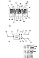
【図面の簡単な説明】
【図1】(a)本発明の実施の形態1における弾性表面波フィルタの構成図
(b)本発明の実施の形態1における平衡型フィルタデバイスの構成図
【図2】本発明の実施の形態1における平衡型フィルタデバイスの特性図
(a)通過特性
(b)振幅バランス特性
(c)位相バランス特性
【図3】本発明の実施の形態1における弾性表面波フィルタの第1の電極構成図
【図4】本発明の実施の形態1における弾性表面波フィルタの第2の電極構成図
【図5】本発明の実施の形態2における平衡型フィルタデバイスの構成図
【図6】本発明の実施の形態3における平衡型フィルタデバイスの構造図
【図7】本発明の実施の形態4における平衡型フィルタデバイスの構造断面図
【図8】本発明の実施の形態4における平衡型フィルタデバイスの構造の分解斜視図
【図9】従来の弾性表面波フィルタの電極構成図
【図10】従来の弾性表面波フィルタの特性図(a)通過特性
(b)振幅バランス特性
(c)位相バランス特性
【図11】本発明の実施の形態5における複合電子部品のブロック図
【図12】本発明の実施の形態5における複合電子部品の分解斜視図
【図13】本発明の実施の形態5における複合電子部品(表側)の説明図(図13(a))、および複合電子部品(裏側)の説明図(図13(b))
【図14】本発明の実施の形態5における複合電子部品の回路図
【図15】本発明の実施の形態1〜4における平衡型フィルタデバイスの他の例の構成図
【図16】本発明の高周波素子の他の例を示す図
【図17】本発明の高周波デバイスを搭載した通信装置を示す図
【符号の説明】
101 弾性表面波フィルタ
102,103,104 IDT電極
105,106 反射器電極
107,108 弾性表面波共振器
109 不平衡型入出力端子
110,111 平衡型入出力端子
112 第1のインダクタ
113 第1の入出力端子
114 第2の入出力端子
115 第3の入出力端子
116 第2のインダクタ[0001]
TECHNICAL FIELD OF THE INVENTION
The present invention relates to a high-frequency device or the like used as a surface acoustic wave filter and a composite electronic component for use in, for example, a mobile phone.
[0002]
[Prior art]
2. Description of the Related Art In recent years, with the development of mobile communication, higher performance and smaller size of components used are expected. Furthermore, the balancing of semiconductor components such as ICs has been progressing for the purpose of improving the noise immunity, and there is a demand for a filter used in the RF stage to be balanced. 2. Description of the Related Art Conventionally, a surface acoustic wave filter has been widely used as a filter in an RF stage of a mobile communication device or the like. In particular, the longitudinal mode type surface acoustic wave filter can easily realize balanced-unbalanced conversion due to the configuration of the interdigital transducer electrode, and has a low loss, high attenuation, and good performance as an RF stage filter having balanced input / output terminals. The balance characteristics are expected.
[0003]
Hereinafter, a conventional longitudinal mode type surface acoustic wave filter having balanced input / output terminals will be described.
[0004]
FIG. 9A shows a configuration of a conventional longitudinal mode type surface acoustic wave filter having balanced input / output terminals (for example, see Patent Document 1). In FIG. 9A, a surface
[0005]
With the above configuration, a surface acoustic wave filter having an unbalanced-balanced input / output terminal can be obtained. In practice, the unbalanced input /
[0006]
In FIG. 9B, a
[0007]
Regarding such a filter, in order to obtain a good balance characteristic, the design and layout of each of the
[0008]
FIG. 10 is a characteristic diagram of the conventional surface acoustic wave filter shown in FIG. However, the one operating in the 1800 MHz band is shown as an example. In FIG. 10, (a) shows the pass characteristic, (b) shows the amplitude balance characteristic in the pass band (from 1805 MHz to 1880 MHz), and (c) shows the phase balance characteristic in the pass band. Here, the amplitude balance characteristic means that the signal amplitude between one of the
[0009]
The phase balance characteristic refers to the phase of the signal between the
[0010]
This time, the balance characteristics shown in FIGS. 10B and 10C are obtained when the
[0011]
[Patent Document 1]
JP-A-6-204781
[0012]
[Problems to be solved by the invention]
However, in the above-described surface acoustic wave filter, in spite of its symmetrical structure, as shown in FIG. 10, in the pass band, the amplitude balance characteristic is −0.3 dB to +1.4 dB, and the phase balance characteristic is −14 ° to −14 dB. This is 1 °, and there is a problem that the balance characteristic, which is one of important electrical characteristics, is greatly deteriorated.
[0013]
This is because the deterioration of the balance characteristic is caused not only by the structure but also by the coupling between the input and output IDT electrodes due to the parasitic component.
[0014]
For example, in the surface
[0015]
For example, in a frequency band such as the 800 MHz to 900 MHz band, the balance characteristic hardly deteriorates. However, if the system supports a high frequency, signal transmission / reception is used even in a high frequency region such as the above 1800 MHz. Therefore, as the frequency handled by the filter increases, this effect cannot be ignored, and a design taking this into consideration is required.
[0016]
However, for example, when viewed from the unbalanced input /
[0017]
Further, the deterioration of the balance characteristic may occur not only in a surface acoustic wave filter but also in a filter such as a cylindrical filter or a dielectric filter, for which it is easy to design the layout symmetrically, in a balanced filter. There was a need for an effective solution.
[0018]
The present invention has been made in view of the above problems, and relates to a high-frequency device having a built-in high-frequency element that operates in a high-frequency band having a balanced input / output terminal. The purpose is to obtain the used communication equipment.
[0019]
[Means for Solving the Problems]
In order to achieve the above object, a first present invention provides a high-frequency element having at least one pair of balanced terminals,
An external input / output terminal connected to a terminal of the high-frequency element,
The high-frequency devices have different impedance values between the pair of balanced terminals and the external input / output terminals respectively connected to the pair of balanced terminals.
[0020]
Further, in the second aspect of the present invention, one of the balanced type terminals of the high-frequency element, one of which is relatively advanced in phase with respect to the other, is larger in the impedance values. 1 is a high-frequency device according to a first aspect of the present invention.
[0021]
Further, a third aspect of the present invention is a first aspect of the present invention, wherein the first input terminal is provided between at least one of the pair of balanced terminals and the external input / output terminal connected to the one of the pair of balanced terminals. 9 is a high-frequency device according to a second embodiment of the present invention including a reactance element.
[0022]
A fourth aspect of the present invention is a method according to the first aspect, wherein the first terminal is provided between the other of the pair of balanced terminals and the external input / output terminal connected to the other of the pair of balanced terminals. A third high-frequency device according to the present invention, further comprising a second reactance element having an impedance value different from that of the second reactance element.
[0023]
In a fifth aspect of the present invention, the first reactance element and / or the second reactance element are realized as an inductance component of a wire when the high-frequency element is mounted on the high-frequency device by wire bonding. A third or fourth high-frequency device according to the present invention.
[0024]
A sixth invention provides the high-frequency device according to the fourth invention, wherein a value obtained by normalizing a difference between an impedance value of the first reactance element and an impedance value of the second reactance element by a termination impedance is 0.2 or less. It is.
[0025]
A seventh aspect of the present invention provides a surface electrode provided on one main surface, at least one inner layer electrode provided in the inner layer, and a via-hole electrode connecting the surface electrode and the inner layer electrode. And a laminated substrate having
The external input / output terminal is realized as the surface electrode,
The high-frequency element is mounted on the other main surface of the substrate,
The first reactance element and / or the second reactance element is a third or fourth high-frequency device according to the present invention realized by an inductance component of the inner layer electrode.
[0026]
Also, in the eighth invention, one end is connected between at least one of the pair of balanced terminals and the external input / output terminal connected to the one of the pair of balanced terminals, A second high-frequency device according to the present invention, comprising a first susceptance element whose other end is grounded.
[0027]
Further, a ninth aspect of the present invention is characterized in that one end is connected between the other of the pair of balanced terminals and the external input / output terminal connected to the other of the pair of balanced terminals. An eighth high-frequency device according to the present invention, comprising a second susceptance element having an end grounded and having an admittance value different from that of the first susceptance element.
[0028]
A tenth aspect of the present invention is the high-frequency device according to the ninth aspect, wherein a value obtained by standardizing a difference between an admittance value of the first susceptance element and an admittance value of the second susceptance by a termination impedance is 5 or more.
[0029]
Further, an eleventh aspect of the present invention provides a method for manufacturing a semiconductor device, comprising the steps of:
An interlayer electrode provided between the dielectric layers,
A via-hole conductor provided over a plurality of the dielectric layers, connecting all or a part of the interlayer electrode,
The interlayer electrode and the via-hole conductor form a plurality of strip lines and a plurality of capacitors,
The first reactance element and the second reactance element are a high-frequency device according to a fourth aspect of the present invention, comprising the plurality of strip lines, the plurality of capacitors, and the via-hole conductor.
[0030]
Further, a twelfth aspect of the present invention includes a plurality of stacked dielectric layers,
An interlayer electrode provided between the dielectric layers,
A via-hole conductor provided over a plurality of the dielectric layers, connecting all or a part of the interlayer electrode,
The interlayer electrode and the via-hole conductor form a plurality of strip lines and a plurality of capacitors,
The first susceptance element and the second susceptance element are a high-frequency device according to a fourth aspect of the present invention, comprising the plurality of strip lines, the plurality of capacitors, and the via-hole conductor.
[0031]
A thirteenth aspect of the present invention is the high-frequency device according to the first aspect, wherein said high-frequency element is a high-frequency filter.
[0032]
Further, a fourteenth aspect of the present invention provides the high frequency filter,
A piezoelectric substrate,
A high-frequency device according to a thirteenth aspect of the present invention, which is a surface acoustic wave filter including at least one interdigital transducer electrode provided on the piezoelectric substrate.
[0033]
Further, a fifteenth aspect of the present invention includes first and second routing electrodes provided between the interdigital transducer electrode and each of the pair of balanced terminals formed on the piezoelectric substrate. ,
A fourteenth high-frequency device according to the present invention, wherein the first and second routing electrodes have different shapes or lengths.
[0034]
In a sixteenth aspect, the interdigital transducer electrode includes at least first, second, and third three interdigital transducer electrodes,
The surface acoustic wave filter is a balanced surface acoustic wave filter using at least two of the interdigital transducer electrodes,
One electrode finger of the first interdigital transducer electrode is connected to an unbalanced input / output terminal, the other electrode finger is grounded,
One electrode finger of the second interdigital transducer electrode is connected to one first terminal of the pair of balanced terminals, and the other electrode finger is grounded;
One electrode finger of the third interdigital transducer electrode is connected to the other second terminal of the pair of balanced terminals, and the other electrode finger is grounded. Device.
[0035]
According to a seventeenth aspect of the present invention, the interdigital transducer electrode includes at least first, second, and third three interdigital transducer electrodes,
The surface acoustic wave filter is a balanced surface acoustic wave filter using at least two of the interdigital transducer electrodes,
One electrode finger of the first interdigital transducer electrode is connected to one first terminal of the pair of balanced terminals, and the other electrode finger is connected to the other of the pair of terminals of the balanced type. 2 terminal,
One electrode finger of the second and third interdigital transducer electrodes is connected to a common unbalanced input / output terminal, and the other electrode ground is a fourteenth high-frequency device of the present invention. .
[0036]
An eighteenth aspect of the present invention provides a first resonator connected between one of the second electrode fingers and the first terminal,
A sixteenth or seventeenth high-frequency device according to the present invention, comprising: one of the third electrode fingers; and a second resonator connected to the second terminal.
[0037]
A nineteenth invention is the high-frequency device according to the eighteenth invention, wherein the shapes of the first resonator and the second resonator are different from each other.
[0038]
A twentieth aspect of the present invention is the high-frequency device according to the first aspect of the present invention, further comprising an inductor connecting one of the pair of balanced terminals and the other of the balanced terminals.
[0039]
Further, a twenty-first aspect of the present invention includes a transmitting unit and / or a receiving unit,
The transmission means or the reception means is a communication device using any one of the first to twentieth high-frequency devices of the present invention.
[0040]
Note that the inductor may be mounted as a component on the surface layer of the multilayer body.
[0041]
Further, the inductor may be constituted by the plurality of strip lines and the via-hole conductor formed in the laminated body layer.
[0042]
BEST MODE FOR CARRYING OUT THE INVENTION
Hereinafter, embodiments of the present invention will be described with reference to the drawings.
[0043]
(Embodiment 1)
First, a balanced filter device according to a first embodiment of the present invention will be described with reference to FIG. FIG. 1A shows the configuration of a surface acoustic wave filter having balanced input / output terminals according to the present embodiment, and FIG. 1B shows the configuration of the surface acoustic wave filter shown in FIG. 1 shows a configuration of a balanced filter device.
[0044]
In FIG. 1A, a surface
[0045]
Here, the first and second surface
[0046]
One
[0047]
Further, the first surface
[0048]
In the
[0049]
Further, a
[0050]
Further, a
[0051]
FIG. 2 shows specific characteristics of the
[0052]
Here, the balance characteristics shown in FIGS. 2B and 2C show characteristics when the second input /
[0053]
Here, the impedance of the
[0054]
In this embodiment, the case where the conventional characteristic is degraded to the minus side is described as an example. However, if the conventional characteristic is degraded to the plus side, the third input /
[0055]
In the present embodiment, a case where the value normalized by the terminating impedance of the
[0056]
In this embodiment, FIG. 1A has been described as the configuration of the surface acoustic wave filter. However, as shown as the surface
[0057]
Alternatively, as shown in a surface
[0058]
That is, even if the built-in surface acoustic wave filter has deteriorated phase balance characteristics as in the conventional example, the
[0059]
In the present embodiment, the
[0060]
(Embodiment 2)
Second Embodiment A high-frequency filter device according to a second embodiment of the present invention will be described with reference to FIG. FIG. 5 shows the configuration of a high-frequency filter device having balanced input / output terminals according to the present embodiment.
[0061]
In FIG. 5, the balanced filter device according to the present embodiment includes IDT electrodes, reflector electrodes, surface acoustic wave resonators, and the like, which are equivalent to the surface
[0062]
Further, a
[0063]
Here, one
[0064]
On the other hand, if the
[0065]
That is, by connecting different reactance components to the first and
[0066]
Specifically, in FIG. 10C, since the phase balance characteristic is degraded from 0 ° to the minus side, the phase balance characteristic is connected to the third input /
[0067]
In the present embodiment, the case where the conventional characteristic is degraded to the minus side is described as an example. However, if the conventional characteristic is degraded to the plus side, the third input /
[0068]
In the present embodiment, a case where the difference between the values normalized by the terminating impedances of the
[0069]
In the present embodiment, the case where the configuration of the surface acoustic wave filter is the same as that shown in FIG. 1A has been described, but the configuration of the surface acoustic wave filter having the configuration shown in FIGS. Similar effects can be obtained.
[0070]
In the present embodiment, the
[0071]
(Embodiment 3)
Next, a specific structure of the balanced filter device according to the third embodiment of the present invention will be described with reference to FIG.
[0072]
In FIG. 6, a
[0073]
Further, first to
[0074]
Here, the
[0075]
Therefore, when mounting on the
[0076]
In the present embodiment, the reactance component is formed using a wire, but the same effect can be obtained by forming the reactance component using a routing electrode on a piezoelectric substrate. Only at this time, the
[0077]
Also, by changing the shapes of the first surface
[0078]
(Embodiment 4)
Embodiment 4 A balanced filter device according to
[0079]
7, a
[0080]
Further, the
[0081]
FIG. 8 is an exploded perspective view showing the specific configuration of FIG. The
[0082]
[0083]
The unbalanced input / output terminal of the surface acoustic wave filter formed on the
[0084]
The
[0085]
The
[0086]
The
[0087]
The
[0088]
Here, since the
[0089]
That is, in the equivalent circuit shown in FIG. 5, the
[0090]
Therefore, when the surface acoustic wave filter is mounted on a small laminated package substrate, each of the pair of input / output terminals of the balanced type input / output terminal of the surface acoustic wave filter depends on the shape of the internal electrode formed in the laminated body layer. , Different inductor components can be connected. Therefore, by connecting different inductors to the balanced input / output terminals, it is possible to obtain a characteristic in which the phase balance characteristic is improved as shown in FIG.
[0091]
In the first to fourth embodiments, the reactance component has been described. However, a susceptance element between the first terminal of the balanced type input / output terminal and the ground and between the second terminal and the ground. Typically, it is also possible to connect a capacitor.
[0092]
FIG. 15 shows a configuration of a balanced filter device when a susceptance element is connected. In the figure, the same or corresponding parts as those in FIG. 5 are denoted by the same reference numerals, and detailed description thereof will be omitted. The
[0093]
Further, the
[0094]
The
[0095]
In such a configuration, when the phase balance characteristic is measured with the surface
[0096]
Further, the
[0097]
At this time, a greater effect can be obtained if the value obtained by standardizing the admittance of the susceptance element connected to the first terminal and the second terminal by the terminal impedance is 5 or more.
[0098]
Furthermore, the
[0099]
Further, when the mounting as shown in FIGS. 7 and 8 is performed, the load value can be changed without changing the device size by using the capacitance component generated by the wiring or the like on the laminated package substrate or the piezoelectric substrate. Becomes possible.
[0100]
(Embodiment 5)
Fourth Embodiment A composite electronic component according to a fourth embodiment of the present invention will be described with reference to FIGS. FIG. 11 is a block diagram of the composite electronic component in the present embodiment, and FIG. 12 is an exploded perspective view of the composite electronic component in the present embodiment (however, shown in the drawing below the dielectric layer DL1). FIG. 13A is an explanatory view of the composite electronic component (front side) according to the present embodiment, and FIG. 13B is a diagram illustrating the composite electronic component according to the present embodiment. FIG. 14 is an explanatory diagram of the electronic component (back side), and FIG. 14 is a circuit diagram of the composite electronic component according to the present embodiment.
[0101]
Composite
[0102]
Here, those using PIN diodes as the transmission /
[0103]
In FIG. 12, the composite electronic component of the present embodiment includes 15 dielectric layers DL1 to DL15. The number of stacked dielectric layers is appropriately selected according to the required characteristics of the composite electronic component.
[0104]
As the dielectric layer, a so-called glass ceramic substrate in which a low melting point glass frit is mixed with a ceramic powder such as a forsterite-based compound or a compound mainly containing alumina can be used. In addition, a green sheet formed by mixing a ceramic powder with an organic binder and an organic solvent was formed into a green sheet, and a large number of via holes for electrically connecting the multilayer wirings were formed by mechanical punching or laser processing. Have been.
[0105]
On a predetermined green sheet, printing is performed using a conductive paste containing silver (or gold or copper) powder as a main component of a conductor to form a wiring pattern, and a wiring pattern of each green sheet is formed. A strip line and a capacitor electrode are formed by printing and filling a conductive paste in a via hole for interlayer connection.
[0106]
The thus obtained fifteen-layer green sheets are accurately positioned, and the dielectric layers DL1 to DL15 are sequentially laminated, and heated and pressed under certain conditions to form an integrated laminated body. 1200 can be obtained. After drying the laminate, the laminate is fired at 400 to 500 degrees in a firing furnace in an oxidizing atmosphere to burn out the organic binder in the green sheet, and as a main component of the conductor, (1) powder of gold or silver (2) baking in a temperature range of about 850 to 950 ° C. in normal air when using (2) copper powder in an inert gas or reducing atmosphere when using copper powder, The laminate 1200 can be obtained.
[0107]
As shown in FIG. 13, an unbalanced input-balanced output SAW filter SF1 to SF2, a diode D1 are provided on the upper surface of a
[0108]
Further, a plurality of terminals T1 for surface mounting the composite electronic component on the main board of the electronic device are formed on the back surface of the dielectric layer DL1. The terminals T1 and T2 are formed by printing and patterning the above-described conductive paste.
[0109]
Next, a laminated structure of a wiring pattern of a composite electronic component having such a multilayer structure will be described with reference to some examples.
[0110]
Ground electrodes G1, G2, G3 are formed on the first, seventh and fourteenth dielectric layers DL1, DL7, DL14 by printing or the like, and a via hole electrode Vg1 is electrically connected to the ground electrodes G1, G2, G3. In order to achieve this, they are appropriately arranged on the second to fourteenth dielectric layers DL2 to DL14. Further, among the terminals T1 arranged on the back surface of the first dielectric layer DL1, the ground terminal electrode Tg1 and the ground electrode G1 are also electrically connected via the via hole electrode Vg1.
[0111]
The strip line electrode pattern on the fourteenth dielectric layer DL14 is interlayer-connected to the strip line electrode pattern on the thirteenth dielectric layer DL13 via the via hole electrodes Vp11 and Vp21. The strip line electrode pattern of the thirteenth dielectric layer DL13 is interlayer-connected to the strip line pattern of the twelfth dielectric layer DL12 via via hole electrodes Vp12 and Vp22. In this manner, for example, the strip line L1 and the strip line L2 are sequentially connected via the ninth to fourteenth dielectric layers DL9 to DL14 via the via-hole electrodes, respectively.
[0112]
The capacitors C1 and C2 are provided with an electrode pattern of the capacitor C1 on the eleventh dielectric layer DL11, and provided on the tenth dielectric layer DL10 with an electrode pattern shared by the capacitors C1 and C2. By providing the electrode pattern of the capacitor C2 on the body layer DL9, they are connected in series.
[0113]
Similarly, by appropriately arranging the respective strip line electrode patterns, capacitor electrode patterns, and via hole electrodes and appropriately electrically connecting to the diodes and the like mounted on the surface layer of the
[0114]
In this way, the configuration of the strip line and the capacitor is performed. However, since the input / output terminals of the composite electronic component in the present embodiment are all gathered on the back surface of the first dielectric layer DL1 via the via holes. In addition, the mounting area when mounted on the main board of the electronic device can be reduced.
[0115]
Here, the connection relationship between the balanced type input / output terminal of the surface acoustic wave filter SF2 and the laminated internal layer electrode will be described in detail. The surface acoustic wave filter SF2 is electrically connected to the terminal T1 formed on the surface layer of the
[0116]
On the other hand, the strip line Ld11 is connected to the strip line Ld12 formed on the thirteenth dielectric layer DL13, the strip line Ld13 formed on the twelfth dielectric layer DL12, and the first to fourteenth dielectric layers DL1 to DL14. The via hole electrode Vd1 is connected to a terminal T1 formed on the bottom surface of the
[0117]
Here, since the strip lines Ld11, Ld12, Ld13, Ld21 and the via-hole electrodes Vd1, Vd2 have inductor components, it is possible to configure an inductor having a desired value by adjusting the length and width of each electrode. It becomes possible. Accordingly, one of the balanced type input / output terminals is connected to the strip line Ld21 formed in the inner layer of the
[0118]
That is, regarding the balanced input / output terminal portion of the surface acoustic wave filter, if the surface acoustic wave filter SF2 is the surface
[0119]
Therefore, it is possible to mount the surface acoustic wave filter on the laminate, and to configure different inductor components depending on the shapes of the strip lines and the via-hole electrodes formed in the laminate inner layer. Therefore, by connecting different inductors to the balanced input / output terminals, it is possible to obtain a characteristic in which the phase balance characteristic is improved as shown in FIG.
[0120]
Further, when the composite electronic component of the present embodiment is used for a mobile phone, for example, it is mounted on a main substrate constituting a wireless circuit. In this case, a composite of a laminate and a surface acoustic wave filter is realized. Therefore, the mounting area can be significantly reduced as compared with the related art, and the size and height of the mobile phone can be reduced.
[0121]
In the present embodiment, the load impedances are made different from each other by connecting different strip lines to the pair of input / output terminals of the balanced input / output terminals, respectively. The same effect can be obtained by connecting capacitors having different impedances between each of them and the ground. In this case, the balanced filter device having the susceptance element shown in FIG. 15 is realized.
[0122]
In this embodiment, the case where two surface acoustic wave filters are mounted has been described as an example. However, only one surface acoustic wave filter is mounted, or three or more surface acoustic wave filters are mounted. The same effect can be obtained in this case.
[0123]
In the present embodiment, the case where the system is used in a combination of three systems of EGSM, DCS, and PCS has been described as an example. However, another system combination, such as EGSM, DCS, and UMTS (Universal Mobile Telecommunications System). Such combinations can be used in the same manner.
[0124]
In this embodiment, a triple band composite electronic component using three communication systems has been described as an example. However, by changing the configuration of the switch circuit, two communication systems (eg, EGSM and UMTS) are used. A similar effect can be obtained in the case of a high-frequency switch using a dual-band composite electronic component or four or more systems (eg, EGSM, Advanced Mobile Phone Service (AMPS), DCS, PCS).
[0125]
Note that, in this embodiment, a case where a diode is used as a switch circuit has been described as an example. However, a case where a GaAs switch is used for only one switch circuit, or a case where a GaAs switch is used for both switch circuits is used. Similar effects can be obtained.
[0126]
In the embodiment of the present invention, a composite electronic component with a high-frequency switch has been described as an example. However, a similar effect can be obtained with a composite electronic component with another high-frequency circuit such as a low-pass filter or a band-pass filter.
[0127]
In each of the above embodiments, the
[0128]
The surface acoustic wave filters 101, 301, 401, 500, and SF2 are examples of the high-frequency device of the present invention.
[0129]
The pair of input /
[0130]
Further, the
[0131]
Further, the
[0132]
Further, the first surface
[0133]
The
[0134]
However, the present invention is not limited to the above embodiment. In each of the above embodiments, the high-frequency element of the present invention is a surface acoustic wave filter. However, any filter having at least one balanced pair of terminals may be used as a dielectric filter, a multilayer filter, or a bulk wave filter. It may be a filter. In particular, it is desirable to employ the filter used in the 1800 MHz band or the high frequency band of 2 GHz to 10 GHz.
[0135]
Here, FIG. 16 shows an example of such a filter. The
[0136]
Furthermore, the high-frequency element of the present invention is not limited to a filter, and may be applied to a semiconductor element. For example, it can be provided to a low noise amplifier (LNA) having a balance circuit.
[0137]
Furthermore, the present invention may be realized as a communication device equipped with the above high-frequency device.
[0138]
For example, FIG. 17 illustrates a case where a mobile phone is used as an example of a communication device. A
[0139]
In such a mobile phone, the balanced filter device of each of the above embodiments can be used for the RF filters 1711 and 1703. When a semiconductor element is used as a high-frequency element, it can be used for the low-
[0140]
【The invention's effect】
As is clear from the above description, the present invention can provide a high-frequency device or the like having good phase balance characteristics.
[Brief description of the drawings]
FIG. 1 (a) is a configuration diagram of a surface acoustic wave filter according to
(B) Configuration diagram of balanced filter device according to
FIG. 2 is a characteristic diagram of the balanced filter device according to the first embodiment of the present invention.
(A) Pass characteristics
(B) Amplitude balance characteristics
(C) Phase balance characteristics
FIG. 3 is a first electrode configuration diagram of the surface acoustic wave filter according to the first embodiment of the present invention.
FIG. 4 is a second electrode configuration diagram of the surface acoustic wave filter according to
FIG. 5 is a configuration diagram of a balanced filter device according to
FIG. 6 is a structural diagram of a balanced filter device according to
FIG. 7 is a structural sectional view of a balanced filter device according to
FIG. 8 is an exploded perspective view of the structure of a balanced filter device according to
FIG. 9 is a diagram showing an electrode configuration of a conventional surface acoustic wave filter.
FIG. 10 is a characteristic diagram of a conventional surface acoustic wave filter.
(B) Amplitude balance characteristics
(C) Phase balance characteristics
FIG. 11 is a block diagram of a composite electronic component according to a fifth embodiment of the present invention.
FIG. 12 is an exploded perspective view of a composite electronic component according to a fifth embodiment of the present invention.
FIG. 13 is an explanatory view of a composite electronic component (front side) according to
FIG. 14 is a circuit diagram of a composite electronic component according to a fifth embodiment of the present invention.
FIG. 15 is a configuration diagram of another example of the balanced filter device according to
FIG. 16 is a diagram showing another example of the high-frequency device of the present invention.
FIG. 17 is a diagram showing a communication device equipped with the high-frequency device of the present invention.
[Explanation of symbols]
101 surface acoustic wave filter
102,103,104 IDT electrode
105,106 reflector electrode
107,108 Surface acoustic wave resonator
109 unbalanced input / output terminal
110,111 balanced input / output terminals
112 First inductor
113 first input / output terminal
114 second input / output terminal
115 third input / output terminal
116 Second inductor
Claims (21)
前記高周波素子の端子と接続された外部入出力端子とを備え、
前記平衡型の一対の端子と、その平衡型の一対の端子にそれぞれ接続された前記外部入出力端子との間の各インピーダンス値は互いに異なる高周波デバイス。A high-frequency device having at least one balanced pair of terminals,
An external input / output terminal connected to a terminal of the high-frequency element,
A high-frequency device in which impedance values between the pair of balanced terminals and the external input / output terminals connected to the pair of balanced terminals are different from each other.
前記外部入出力端子は、前記表層電極として実現され、
前記高周波素子は、前記基板の他方の主面上に実装され、
前記第1のリアクタンス素子および/または第2のリアクタンス素子は、前記内層電極によるインダクタンス成分で実現されている請求項3または4に記載の高周波デバイス。A surface layer electrode provided on one main surface, at least one or more inner layer electrodes provided in the inner layer, and a laminated substrate having a via hole electrode connecting the surface layer electrode and the inner layer electrode,
The external input / output terminal is realized as the surface electrode,
The high-frequency element is mounted on the other main surface of the substrate,
The high-frequency device according to claim 3, wherein the first reactance element and / or the second reactance element is realized by an inductance component of the inner layer electrode.
前記誘電体層間に設けられた層間電極と、
前記層間電極の全部または一部を接続する、複数の前記誘電体層にまたがって設けられたビアホール導体とを備え、
前記層間電極および前記ビアホール導体は、複数のストリップラインおよび複数のコンデンサを形成し、
前記第1のリアクタンス素子および第2のリアクタンス素子は、前記複数のストリップライン、前記複数のコンデンサおよび前記ビアホール導体により構成されている請求項4に記載の高周波デバイス。A plurality of stacked dielectric layers,
An interlayer electrode provided between the dielectric layers,
A via-hole conductor provided over a plurality of the dielectric layers, connecting all or a part of the interlayer electrode,
The interlayer electrode and the via-hole conductor form a plurality of strip lines and a plurality of capacitors,
The high-frequency device according to claim 4, wherein the first reactance element and the second reactance element are configured by the plurality of strip lines, the plurality of capacitors, and the via-hole conductor.
前記誘電体層間に設けられた層間電極と、
前記層間電極の全部または一部を接続する、複数の前記誘電体層にまたがって設けられたビアホール導体とを備え、
前記層間電極および前記ビアホール導体は、複数のストリップラインおよび複数のコンデンサを形成し、
前記第1のサセプタンス素子および第2のサセプタンス素子は、前記複数のストリップライン、前記複数のコンデンサおよび前記ビアホール導体により構成されている請求項4に記載の高周波デバイス。A plurality of stacked dielectric layers,
An interlayer electrode provided between the dielectric layers,
A via-hole conductor provided over a plurality of the dielectric layers, connecting all or a part of the interlayer electrode,
The interlayer electrode and the via-hole conductor form a plurality of strip lines and a plurality of capacitors,
The high-frequency device according to claim 4, wherein the first susceptance element and the second susceptance element are configured by the plurality of strip lines, the plurality of capacitors, and the via-hole conductor.
圧電基板と、
前記圧電基板上に設けられた、少なくとも一つのインターディジタルトランスデューサ電極とを備えた弾性表面波フィルタである請求項13に記載の高周波デバイス。The high frequency filter,
A piezoelectric substrate,
The high-frequency device according to claim 13, wherein the high-frequency device is a surface acoustic wave filter including at least one interdigital transducer electrode provided on the piezoelectric substrate.
前記第1および第2の引き回し電極の形状又は長さが異なる請求項14に記載の高周波デバイス。A first and a second routing electrode provided between the interdigital transducer electrode and each of the pair of balanced terminals formed on the piezoelectric substrate;
The high-frequency device according to claim 14, wherein the first and second routing electrodes have different shapes or lengths.
前記弾性表面波フィルタは、少なくとも2つの前記インターディジタルトランスデューサ電極を用いた平衡型の弾性表面波フィルタであって、
前記第1のインターディジタルトランスデューサ電極の一方の電極指は不平衡型の入出力端子に接続され、他方の電極指は接地され、
前記第2のインターディジタルトランスデューサ電極の一方の電極指は前記平衡型の一対の端子の一方の第1の端子に接続されると共に、他方の電極指は接地され、
前記第3のインターディジタルトランスデューサ電極の一方の電極指は前記平衡型の一対の端子の他方の第2の端子に接続されると共に、他方の電極指は接地されている請求項14に記載の高周波デバイス。The interdigital transducer electrode is comprised of at least first, second and third three interdigital transducer electrodes;
The surface acoustic wave filter is a balanced surface acoustic wave filter using at least two of the interdigital transducer electrodes,
One electrode finger of the first interdigital transducer electrode is connected to an unbalanced input / output terminal, the other electrode finger is grounded,
One electrode finger of the second interdigital transducer electrode is connected to one first terminal of the pair of balanced terminals, and the other electrode finger is grounded;
15. The high-frequency device according to claim 14, wherein one electrode finger of the third interdigital transducer electrode is connected to the other second terminal of the pair of balanced terminals, and the other electrode finger is grounded. device.
前記弾性表面波フィルタは、少なくとも2つの前記インターディジタルトランスデューサ電極を用いた平衡型の弾性表面波フィルタであって、
前記第1のインターディジタルトランスデューサ電極の一方の電極指は前記平衡型の一対の端子の一方の第1の端子に接続されると共に、他方の電極指は前記平衡型の一対の端子の他方の第2の端子に接続され、
前記第2および前記第3のインターディジタルトランスデューサ電極の一方の電極指は、共通の不平衡型の入出力端子に接続されると共に、他方は接地されている請求項14に記載の高周波デバイス。The interdigital transducer electrode is comprised of at least first, second and third three interdigital transducer electrodes;
The surface acoustic wave filter is a balanced surface acoustic wave filter using at least two of the interdigital transducer electrodes,
One electrode finger of the first interdigital transducer electrode is connected to one first terminal of the pair of balanced terminals, and the other electrode finger is connected to the other of the pair of terminals of the balanced type. 2 terminal,
The high-frequency device according to claim 14, wherein one electrode finger of the second and third interdigital transducer electrodes is connected to a common unbalanced input / output terminal, and the other is grounded.
前記第3の電極指の一方と前記第2の端子に接続された第2の共振器とを備えた請求項16または17に記載の高周波デバイス。A first resonator connected between one of the second electrode fingers and the first terminal;
The high-frequency device according to claim 16, further comprising one of the third electrode fingers and a second resonator connected to the second terminal.
前記送信手段または前記受信手段は、請求項1から20のいずれかに記載の高周波デバイスを用いた通信機器。Comprising transmitting means and / or receiving means,
A communication device using the high-frequency device according to any one of claims 1 to 20, wherein said transmission means or said reception means.
Priority Applications (1)
| Application Number | Priority Date | Filing Date | Title |
|---|---|---|---|
| JP2003108328A JP2004007575A (en) | 2002-04-15 | 2003-04-11 | High frequency device, and communication apparatus |
Applications Claiming Priority (2)
| Application Number | Priority Date | Filing Date | Title |
|---|---|---|---|
| JP2002112564 | 2002-04-15 | ||
| JP2003108328A JP2004007575A (en) | 2002-04-15 | 2003-04-11 | High frequency device, and communication apparatus |
Publications (2)
| Publication Number | Publication Date |
|---|---|
| JP2004007575A true JP2004007575A (en) | 2004-01-08 |
| JP2004007575A5 JP2004007575A5 (en) | 2006-04-13 |
Family
ID=30447033
Family Applications (1)
| Application Number | Title | Priority Date | Filing Date |
|---|---|---|---|
| JP2003108328A Pending JP2004007575A (en) | 2002-04-15 | 2003-04-11 | High frequency device, and communication apparatus |
Country Status (1)
| Country | Link |
|---|---|
| JP (1) | JP2004007575A (en) |
Cited By (6)
| Publication number | Priority date | Publication date | Assignee | Title |
|---|---|---|---|---|
| JP2005210470A (en) * | 2004-01-23 | 2005-08-04 | Soshin Electric Co Ltd | Passive component |
| JP2006074749A (en) * | 2004-08-04 | 2006-03-16 | Matsushita Electric Ind Co Ltd | Antenna duplexer, and rf module and communication apparatus using the same |
| WO2006137248A1 (en) * | 2005-06-21 | 2006-12-28 | Murata Manufacturing Co., Ltd. | Saw splitter |
| US7233219B2 (en) | 2004-04-28 | 2007-06-19 | Fujitsu Media Devices Limited | Balanced output filter having specified package input and output ground metal patterns |
| US7701311B2 (en) | 2004-08-04 | 2010-04-20 | Panasonic Corporation | Antenna duplexer, and RF module and communication apparatus using the same |
| JP2012129921A (en) * | 2010-12-17 | 2012-07-05 | Kyocera Corp | Elastic wave device |
-
2003
- 2003-04-11 JP JP2003108328A patent/JP2004007575A/en active Pending
Cited By (8)
| Publication number | Priority date | Publication date | Assignee | Title |
|---|---|---|---|---|
| JP2005210470A (en) * | 2004-01-23 | 2005-08-04 | Soshin Electric Co Ltd | Passive component |
| US7233219B2 (en) | 2004-04-28 | 2007-06-19 | Fujitsu Media Devices Limited | Balanced output filter having specified package input and output ground metal patterns |
| JP2006074749A (en) * | 2004-08-04 | 2006-03-16 | Matsushita Electric Ind Co Ltd | Antenna duplexer, and rf module and communication apparatus using the same |
| US7701311B2 (en) | 2004-08-04 | 2010-04-20 | Panasonic Corporation | Antenna duplexer, and RF module and communication apparatus using the same |
| JP4504278B2 (en) * | 2004-08-04 | 2010-07-14 | パナソニック株式会社 | Antenna duplexer, and high-frequency module and communication device using the same |
| WO2006137248A1 (en) * | 2005-06-21 | 2006-12-28 | Murata Manufacturing Co., Ltd. | Saw splitter |
| JPWO2006137248A1 (en) * | 2005-06-21 | 2009-01-08 | 株式会社村田製作所 | SAW duplexer |
| JP2012129921A (en) * | 2010-12-17 | 2012-07-05 | Kyocera Corp | Elastic wave device |
Similar Documents
| Publication | Publication Date | Title |
|---|---|---|
| US7084718B2 (en) | Band elimination filter, filter device, antenna duplexer and communication apparatus | |
| US7283016B2 (en) | Balanced acoustic wave filter and acoustic wave filter | |
| US7924118B2 (en) | Duplexer and elastic wave device | |
| US6943645B2 (en) | Surface acoustic wave duplexer and communication apparatus having the same | |
| US7498899B2 (en) | Duplexer with filters including film bulk acoustic resonators | |
| JP3960551B2 (en) | Antenna duplexer and communication telephone using the same | |
| US20200195228A1 (en) | Multiplexer, transmission apparatus, and reception apparatus | |
| JP5355958B2 (en) | Filters, duplexers, and communication equipment | |
| US20070046395A1 (en) | Duplexer having matching circuit | |
| JP4634861B2 (en) | Surface acoustic wave device and communication device | |
| US7629863B2 (en) | Filter and duplexer | |
| US20120286895A1 (en) | Ladder filter, duplexer and module | |
| EP1300946A2 (en) | High frequency switch and radio communication apparatus | |
| US8581674B2 (en) | Filter and communications apparatus | |
| EP1372263A2 (en) | High-frequency device and communication apparatus | |
| JP2004056745A (en) | Compposite high frequency component | |
| WO2006040923A1 (en) | Splitter | |
| US20120068788A1 (en) | Elastic wave apparatus and duplexer | |
| JP2004007575A (en) | High frequency device, and communication apparatus | |
| JP6112654B2 (en) | module | |
| US11239826B2 (en) | Filter device | |
| JP6566170B2 (en) | Multiplexer, high-frequency front-end circuit, and communication device | |
| CN114424459A (en) | Filter device and communication device | |
| US20230208003A1 (en) | Directional coupler, high-frequency module, and communication apparatus | |
| JP2003198419A (en) | High frequency switch and radio communication equipment |
Legal Events
| Date | Code | Title | Description |
|---|---|---|---|
| A521 | Written amendment |
Free format text: JAPANESE INTERMEDIATE CODE: A523 Effective date: 20060227 |
|
| A621 | Written request for application examination |
Free format text: JAPANESE INTERMEDIATE CODE: A621 Effective date: 20060227 |
|
| A131 | Notification of reasons for refusal |
Free format text: JAPANESE INTERMEDIATE CODE: A131 Effective date: 20070911 |
|
| A02 | Decision of refusal |
Free format text: JAPANESE INTERMEDIATE CODE: A02 Effective date: 20080205 |