JP2003197574A5 - - Google Patents
Download PDFInfo
- Publication number
- JP2003197574A5 JP2003197574A5 JP2001398479A JP2001398479A JP2003197574A5 JP 2003197574 A5 JP2003197574 A5 JP 2003197574A5 JP 2001398479 A JP2001398479 A JP 2001398479A JP 2001398479 A JP2001398479 A JP 2001398479A JP 2003197574 A5 JP2003197574 A5 JP 2003197574A5
- Authority
- JP
- Japan
- Prior art keywords
- film
- polishing
- insulating film
- angstroms
- sicn
- Prior art date
- Legal status (The legal status is an assumption and is not a legal conclusion. Google has not performed a legal analysis and makes no representation as to the accuracy of the status listed.)
- Granted
Links
Images
Description
【0002】
【従来の技術】
これまで、LSIの絶縁膜材料としては、SiO 2 やSiNが用いられてきた。特に、SiO 2 は主要な絶縁膜であり、SiNは、例えばSiO 2 をRIEにより除去する時のマスクやストッパーとして、あるいは、水や金属の拡散バリア膜として用いられてきた。[0002]
[Prior Art]
So far, SiO 2 and SiN have been used as insulating film materials for LSIs. In particular, SiO 2 is a main insulating film, and SiN has been used, for example, as a mask or a stopper when SiO 2 is removed by RIE, or as a diffusion barrier film of water or metal.
【0031】
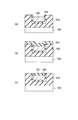
まず、半導体基板100上に絶縁膜101を形成し、この絶縁膜101をパターニングして、深さ3000オングストロームの溝102を形成した。絶縁膜101の構成は、膜厚6000オングストロームの低誘電率絶縁膜(LKD27:JSR社製)103と、膜厚500オングストロームのSiCO膜104の2層構造である。次いで、溝102が形成された絶縁膜101上に、膜厚100オングストロームのTaNライナー105を形成し、更にその上に6000オングストロームのCu膜106を堆積し、溝102内をCu膜で埋めた(図1(a))。なお、Cu膜106は、最初にスパッタ法によりシード層を形成し、次いでこのシード層上に鍍金法により形成した。[0031]
First, the insulating film 101 was formed on the
【0034】
次に、TaNライナー105の溝102の外側にある部分、およびSiCO膜104を研磨により除去した。研磨の条件は、以下の通りである。[0034]
Next, the portion of the
【0035】
研磨スラリー:0.2wt%の過酸化水素(酸化剤)、1wt%のキノリン酸、および3wt%のコロイダルシリカ(平均粒径:20nm)をKOHにてpHを10にコントロールした水分散液、
スラリー流量:200cc/分、
研磨パッド:IC1000(RODEL社)、
荷重:300g/cm2、
キャリアおよびテーブルの回転数:100rpm、
以上の研磨条件で2分間、研磨処理を行なったところ、SiCO膜104を容易に除去することが出来た。その結果、図1(c)に示す構造の低誘電率の絶縁膜103に埋め込まれたCuダマシン配線を得た。[0035]
Polishing slurry: an aqueous dispersion in which 0.2 wt% of hydrogen peroxide (oxidizing agent), 1 wt% of quinolinic acid, and 3 wt% of colloidal silica (average particle size: 20 nm) are controlled to pH 10 with KOH,
Slurry flow rate: 200 cc / min,
Polishing pad: IC 1000 (RODEL),
Load: 300 g / cm 2 ,
Carrier and table speed: 100 rpm,
When the polishing process was performed for 2 minutes under the above polishing conditions, the SiCO film 104 could be easily removed. As a result, a Cu damascene wire embedded in the low dielectric constant
【0036】
実施例2
本発明を、上部にSiCNからなる拡散・酸化防止膜を有するCuダマシン配線の形成に適用した実施例について、図2(a)〜(c)を参照して説明する。[0036]
Example 2
An embodiment in which the present invention is applied to the formation of a Cu damascene wiring having a diffusion / antioxidation film made of SiCN in the upper part will be described with reference to FIGS. 2 (a) to 2 (c).
【0038】
次に、全面に800オングストロームの厚さのSiCN膜201を堆積した。その後、SiCN膜201の、Cuダマシン配線106上を除く部分を研磨により除去した。研磨の条件は、以下の通りである。[0038]
Next, an 800 Å
【0039】
研磨スラリー:1.5wt%のピコリン酸、および5wt%のコロイダルシリカ(平均粒径:15nm)を含有する水分散液(pH:2)、
スラリー流量:200cc/分、
研磨パッド:IC1000(RODEL社)、
荷重:300g/cm2、
キャリアおよびテーブルの回転数:100rpm
以上の研磨条件で2分間、研磨処理を行い、図2(c)に示す構造の、上部にSiCNからなる拡散・酸化防止膜201を有するCuダマシン配線を得た。 このようにして得たCuダマシン配線の層間容量は、全面にSiC膜がある構造に対し、5%の改善がみられた。[0039]
Polishing slurry: aqueous dispersion (pH: 2) containing 1.5 wt% of picolinic acid and 5 wt% of colloidal silica (average particle diameter: 15 nm)
Slurry flow rate: 200 cc / min,
Polishing pad: IC 1000 (RODEL),
Load: 300 g / cm 2 ,
Carrier and table speed: 100 rpm
Polishing was carried out for 2 minutes under the above polishing conditions, to obtain a Cu damascene wire having a diffusion /
Priority Applications (2)
| Application Number | Priority Date | Filing Date | Title |
|---|---|---|---|
| JP2001398479A JP3748410B2 (en) | 2001-12-27 | 2001-12-27 | Polishing method and semiconductor device manufacturing method |
| US10/326,407 US6995090B2 (en) | 2001-12-27 | 2002-12-23 | Polishing slurry for use in CMP of SiC series compound, polishing method, and method of manufacturing semiconductor device |
Applications Claiming Priority (1)
| Application Number | Priority Date | Filing Date | Title |
|---|---|---|---|
| JP2001398479A JP3748410B2 (en) | 2001-12-27 | 2001-12-27 | Polishing method and semiconductor device manufacturing method |
Publications (3)
| Publication Number | Publication Date |
|---|---|
| JP2003197574A JP2003197574A (en) | 2003-07-11 |
| JP2003197574A5 true JP2003197574A5 (en) | 2004-07-08 |
| JP3748410B2 JP3748410B2 (en) | 2006-02-22 |
Family
ID=19189350
Family Applications (1)
| Application Number | Title | Priority Date | Filing Date |
|---|---|---|---|
| JP2001398479A Expired - Fee Related JP3748410B2 (en) | 2001-12-27 | 2001-12-27 | Polishing method and semiconductor device manufacturing method |
Country Status (2)
| Country | Link |
|---|---|
| US (1) | US6995090B2 (en) |
| JP (1) | JP3748410B2 (en) |
Families Citing this family (22)
| Publication number | Priority date | Publication date | Assignee | Title |
|---|---|---|---|---|
| RU2356926C2 (en) * | 2003-07-11 | 2009-05-27 | У.Р. Грэйс Энд Ко.-Конн. | Abrasive particles for mechanical polishing |
| US20050056810A1 (en) * | 2003-09-17 | 2005-03-17 | Jinru Bian | Polishing composition for semiconductor wafers |
| US20080261401A1 (en) * | 2004-04-08 | 2008-10-23 | Ii-Vi Incorporated | Chemical-Mechanical Polishing of Sic Surfaces Using Hydrogen Peroxide or Ozonated Water Solutions in Combination with Colloidal Abrasive |
| US20060108325A1 (en) * | 2004-11-19 | 2006-05-25 | Everson William J | Polishing process for producing damage free surfaces on semi-insulating silicon carbide wafers |
| CN101263583B (en) * | 2005-09-09 | 2010-05-26 | 旭硝子株式会社 | Polishing compound, polishing device, and semiconductor integrated circuit device |
| US7998866B2 (en) * | 2006-09-05 | 2011-08-16 | Cabot Microelectronics Corporation | Silicon carbide polishing method utilizing water-soluble oxidizers |
| US7678700B2 (en) * | 2006-09-05 | 2010-03-16 | Cabot Microelectronics Corporation | Silicon carbide polishing method utilizing water-soluble oxidizers |
| US7723234B2 (en) * | 2006-11-22 | 2010-05-25 | Clarkson University | Method for selective CMP of polysilicon |
| JP4523935B2 (en) * | 2006-12-27 | 2010-08-11 | 昭和電工株式会社 | An aqueous polishing slurry for polishing a silicon carbide single crystal substrate and a polishing method. |
| KR101453082B1 (en) * | 2007-06-15 | 2014-10-28 | 삼성전자주식회사 | Alternating current driving type quantum dot electroluminescence device |
| US9548211B2 (en) | 2008-12-04 | 2017-01-17 | Cabot Microelectronics Corporation | Method to selectively polish silicon carbide films |
| US8980113B2 (en) * | 2009-03-13 | 2015-03-17 | Saint-Gobain Ceramics & Plastics, Inc. | Chemical mechanical planarization using nanodiamond |
| KR101094161B1 (en) | 2009-10-19 | 2011-12-14 | 주식회사 케이씨텍 | Method of manufacturing slurry for chemical mechanical polishing |
| KR101203136B1 (en) * | 2010-03-22 | 2012-11-20 | 국립대학법인 울산과학기술대학교 산학협력단 | Method for manufacturing nano-wire |
| EP2587526A1 (en) * | 2010-06-23 | 2013-05-01 | Nissan Chemical Industries, Ltd. | Composition for polishing silicon carbide substrate and method for polishing silicon carbide substrate |
| KR102050783B1 (en) | 2011-11-25 | 2019-12-02 | 가부시키가이샤 후지미인코퍼레이티드 | Polishing composition |
| JP6068790B2 (en) * | 2011-11-25 | 2017-01-25 | 株式会社フジミインコーポレーテッド | Method for producing polishing composition |
| EP3333232B1 (en) | 2012-05-10 | 2020-03-04 | Versum Materials US, LLC | Chemical mechanical polishing composition having chemical additives and methods for using |
| US8999193B2 (en) | 2012-05-10 | 2015-04-07 | Air Products And Chemicals, Inc. | Chemical mechanical polishing composition having chemical additives and methods for using same |
| US9551075B2 (en) * | 2014-08-04 | 2017-01-24 | Sinmat, Inc. | Chemical mechanical polishing of alumina |
| KR102371795B1 (en) | 2016-09-23 | 2022-03-08 | 생-고뱅 세라믹스 앤드 플라스틱스, 인코포레이티드 | Chemical mechanical planarization slurry and method for forming same |
| CN112029417A (en) * | 2020-09-30 | 2020-12-04 | 常州时创新材料有限公司 | Polishing composition for silicon carbide CMP and preparation method thereof |
Family Cites Families (6)
| Publication number | Priority date | Publication date | Assignee | Title |
|---|---|---|---|---|
| JP3297220B2 (en) * | 1993-10-29 | 2002-07-02 | 株式会社東芝 | Semiconductor device manufacturing method and semiconductor device |
| JP3523107B2 (en) * | 1999-03-17 | 2004-04-26 | 株式会社東芝 | Slurry for CMP and CMP method |
| US6611060B1 (en) * | 1999-10-04 | 2003-08-26 | Kabushiki Kaisha Toshiba | Semiconductor device having a damascene type wiring layer |
| JP3736249B2 (en) | 2000-01-12 | 2006-01-18 | Jsr株式会社 | Chemical mechanical polishing aqueous dispersion used in the manufacture of semiconductor devices |
| KR100481651B1 (en) * | 2000-08-21 | 2005-04-08 | 가부시끼가이샤 도시바 | Slurry for chemical mechanical polishing and method for manufacturing semiconductor device |
| US20040018697A1 (en) * | 2002-07-26 | 2004-01-29 | Chung Henry Wei-Ming | Method and structure of interconnection with anti-reflection coating |
-
2001
- 2001-12-27 JP JP2001398479A patent/JP3748410B2/en not_active Expired - Fee Related
-
2002
- 2002-12-23 US US10/326,407 patent/US6995090B2/en not_active Expired - Fee Related
Similar Documents
| Publication | Publication Date | Title |
|---|---|---|
| JP2003197574A5 (en) | ||
| JP3748410B2 (en) | Polishing method and semiconductor device manufacturing method | |
| TWI233181B (en) | Very low effective dielectric constant interconnect Structures and methods for fabricating the same | |
| US6713873B1 (en) | Adhesion between dielectric materials | |
| US6586334B2 (en) | Reducing copper line resistivity by smoothing trench and via sidewalls | |
| US6376376B1 (en) | Method to prevent CU dishing during damascene formation | |
| US6103625A (en) | Use of a polish stop layer in the formation of metal structures | |
| JP3615205B2 (en) | Semiconductor device and manufacturing method of semiconductor device | |
| US7834459B2 (en) | Semiconductor device and semiconductor device manufacturing method | |
| CN1319148C (en) | Structures with improved interfacial strength of SiCOH dielectrics and method for preparing the same | |
| US6140239A (en) | Chemically removable Cu CMP slurry abrasive | |
| TW200525633A (en) | Multi-step plasma treatment method to improve cu interconnect electrical performance | |
| KR100703968B1 (en) | Method for fabricating interconnection line in a semiconductor device | |
| US6284642B1 (en) | Integrated method of damascene and borderless via process | |
| WO2009070967A1 (en) | A chemical-mechanical polishing liquid | |
| US6251789B1 (en) | Selective slurries for the formation of conductive structures | |
| JP2004146798A (en) | Semiconductor device and manufacturing method therefor | |
| TW444256B (en) | Process for fabricating semiconductor device having reliable conductive layer and interlayer insulating layer | |
| US20220367244A1 (en) | Titanium-containing diffusion barrier for cmp removal rate enhancement and contamination reduction | |
| TW200531193A (en) | Bonding structure and fabrication thereof | |
| JPH1116906A (en) | Semiconductor device and its manufacturing method | |
| US6459155B1 (en) | Damascene processing employing low Si-SiON etch stop layer/arc | |
| JP2004165434A (en) | Manufacturing method for semiconductor device | |
| TWI313495B (en) | Method for forming a metal interconnection layer of a semiconductor device using a modified dual damascene process | |
| JP2001284355A (en) | Semiconductor device and its manufacturing method |