JP2003166047A5 - - Google Patents
Download PDFInfo
- Publication number
- JP2003166047A5 JP2003166047A5 JP2002080873A JP2002080873A JP2003166047A5 JP 2003166047 A5 JP2003166047 A5 JP 2003166047A5 JP 2002080873 A JP2002080873 A JP 2002080873A JP 2002080873 A JP2002080873 A JP 2002080873A JP 2003166047 A5 JP2003166047 A5 JP 2003166047A5
- Authority
- JP
- Japan
- Prior art keywords
- rank
- here
- scratch
- membrane
- sample
- Prior art date
- Legal status (The legal status is an assumption and is not a legal conclusion. Google has not performed a legal analysis and makes no representation as to the accuracy of the status listed.)
- Pending
Links
Images
Description
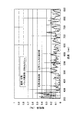
図13(a)に示すように、この試験に用いた耐摩耗性試験装置201は、往復動する可動台202上に試料(薄膜が形成された基板)203を載置し、下面にスチールウール204が配置された押圧子205を試料203に所定の荷重(ここでは700g)で押圧するように構成されている。符号206は押圧子205を保持するアームを示す。また、スチールウール204は、ここでは#0000のものを用いた。耐摩耗性は、図13(b)に示すように、A〜Dの4ランクにランク付けすることによって行った。ここで、ランクAは「傷が付かない」、ランクBは「傷が少し付く」、ランクCは「傷がつき、膜の剥離もある」、ランクDは「膜がほとんど剥離する」というランクである。 As shown in FIG. 13A, the abrasion resistance test apparatus 201 used in this test places the sample (substrate on which the thin film is formed) 203 on the movable table 202 which reciprocates, and the steel wool on the lower surface It is configured to press the pressing element 205, in which 204 is disposed, onto the sample 203 with a predetermined load (here, 700 g). Reference numeral 206 denotes an arm for holding the presser 205. Moreover, the steel wool 204 used here the thing of # 0000 . The abrasion resistance was performed by ranking in four ranks of A to D as shown in FIG. 13 (b). Here, rank A is "scratch-free", rank B is "scratch a bit", rank C is "scratched and there is peeling of the membrane" and rank D is "the membrane almost peels off" It is.
Priority Applications (6)
| Application Number | Priority Date | Filing Date | Title |
|---|---|---|---|
| JP2002080873A JP2003166047A (en) | 2001-09-20 | 2002-03-22 | Method and apparatus for forming film of halogen compound, and magnesium fluoride film |
| TW091120844A TWI276695B (en) | 2001-09-20 | 2002-09-12 | Method and apparatus for forming film of halogen compound, and magnesium fluoride film |
| US10/247,081 US20030068531A1 (en) | 2001-09-20 | 2002-09-19 | Film deposition method and film deposition system for depositing a halogen compound film, and magnesium fluoride film |
| KR10-2002-0057429A KR100498278B1 (en) | 2001-09-20 | 2002-09-19 | Film Deposition Method and Film Deposition System for Depositing a Halogen Compound Film, and Magnesium Fluoride Film |
| CNB021514518A CN1284879C (en) | 2001-09-20 | 2002-09-20 | Film forming method and device for halogen and magnesia fluoride film |
| US10/858,178 US7223449B2 (en) | 2001-09-20 | 2004-06-01 | Film deposition method |
Applications Claiming Priority (3)
| Application Number | Priority Date | Filing Date | Title |
|---|---|---|---|
| JP2001-287114 | 2001-09-20 | ||
| JP2001287114 | 2001-09-20 | ||
| JP2002080873A JP2003166047A (en) | 2001-09-20 | 2002-03-22 | Method and apparatus for forming film of halogen compound, and magnesium fluoride film |
Publications (2)
| Publication Number | Publication Date |
|---|---|
| JP2003166047A JP2003166047A (en) | 2003-06-13 |
| JP2003166047A5 true JP2003166047A5 (en) | 2005-06-09 |
Family
ID=26622600
Family Applications (1)
| Application Number | Title | Priority Date | Filing Date |
|---|---|---|---|
| JP2002080873A Pending JP2003166047A (en) | 2001-09-20 | 2002-03-22 | Method and apparatus for forming film of halogen compound, and magnesium fluoride film |
Country Status (5)
| Country | Link |
|---|---|
| US (2) | US20030068531A1 (en) |
| JP (1) | JP2003166047A (en) |
| KR (1) | KR100498278B1 (en) |
| CN (1) | CN1284879C (en) |
| TW (1) | TWI276695B (en) |
Families Citing this family (14)
| Publication number | Priority date | Publication date | Assignee | Title |
|---|---|---|---|---|
| JP3981281B2 (en) * | 2002-02-14 | 2007-09-26 | 松下電器産業株式会社 | Semiconductor integrated circuit design method and test method |
| USH2212H1 (en) * | 2003-09-26 | 2008-04-01 | The United States Of America As Represented By The Secretary Of The Navy | Method and apparatus for producing an ion-ion plasma continuous in time |
| US7615132B2 (en) * | 2003-10-17 | 2009-11-10 | Hitachi High-Technologies Corporation | Plasma processing apparatus having high frequency power source with sag compensation function and plasma processing method |
| KR100674532B1 (en) * | 2005-02-28 | 2007-01-29 | 한국과학기술연구원 | Method And Apparatus For Forming Metal Film Having Improved Adhesion On The Polymer |
| US7842355B2 (en) * | 2005-11-01 | 2010-11-30 | Applied Materials, Inc. | System and method for modulation of power and power related functions of PECVD discharge sources to achieve new film properties |
| JP4757689B2 (en) * | 2006-03-31 | 2011-08-24 | 株式会社昭和真空 | Film forming apparatus and film forming method |
| US8540851B2 (en) * | 2009-02-19 | 2013-09-24 | Fujifilm Corporation | Physical vapor deposition with impedance matching network |
| JP5504720B2 (en) * | 2009-07-14 | 2014-05-28 | 凸版印刷株式会社 | Deposition equipment |
| WO2011091159A1 (en) * | 2010-01-21 | 2011-07-28 | Roper Scientific, Inc. | Solid state back- illuminated photon sensor and its method of fabrication |
| JP5843491B2 (en) | 2010-06-24 | 2016-01-13 | キヤノン株式会社 | Coating liquid, optical component manufacturing method and photographing optical system |
| US8760054B2 (en) * | 2011-01-21 | 2014-06-24 | Axcelis Technologies Inc. | Microwave plasma electron flood |
| US9957618B2 (en) * | 2012-02-28 | 2018-05-01 | Massachusetts Institute Of Technology | Single-unit reactor design for combined oxidative, initiated, and plasma-enhanced chemical vapor deposition |
| JP7094154B2 (en) * | 2018-06-13 | 2022-07-01 | 東京エレクトロン株式会社 | Film forming equipment and film forming method |
| TWI700967B (en) * | 2019-07-09 | 2020-08-01 | 日商住友重機械工業股份有限公司 | Negative ion generator |
Family Cites Families (16)
| Publication number | Priority date | Publication date | Assignee | Title |
|---|---|---|---|---|
| JPS63106623A (en) * | 1986-10-23 | 1988-05-11 | Fujitsu Ltd | Liquid crystal display element |
| JPH04224136A (en) * | 1990-12-26 | 1992-08-13 | Matsunami Glass Kogyo Kk | Glass material treated with plasma discharge |
| US5756222A (en) * | 1994-08-15 | 1998-05-26 | Applied Materials, Inc. | Corrosion-resistant aluminum article for semiconductor processing equipment |
| JP3585276B2 (en) * | 1994-12-01 | 2004-11-04 | オリンパス株式会社 | Method of manufacturing optical thin film and substrate having this optical thin film |
| JP3808917B2 (en) * | 1995-07-20 | 2006-08-16 | オリンパス株式会社 | Thin film manufacturing method and thin film |
| JPH09243802A (en) | 1996-03-14 | 1997-09-19 | Olympus Optical Co Ltd | Formation of optical thin film and device for forming the same |
| JPH09324262A (en) * | 1996-06-06 | 1997-12-16 | Nikon Corp | Production of fluoride thin film and fluoride thin film |
| US6025585A (en) * | 1996-11-01 | 2000-02-15 | The Regents Of The University Of California | Low-resistivity photon-transparent window attached to photo-sensitive silicon detector |
| JP3987169B2 (en) * | 1997-10-02 | 2007-10-03 | オリンパス株式会社 | Optical thin film manufacturing method |
| TW477009B (en) * | 1999-05-26 | 2002-02-21 | Tadahiro Ohmi | Plasma process device |
| JP2001140067A (en) * | 1999-11-17 | 2001-05-22 | Canon Inc | Method for depositing optical thin film and film deposition system |
| JP4334723B2 (en) * | 2000-03-21 | 2009-09-30 | 新明和工業株式会社 | Ion plating film forming apparatus and ion plating film forming method. |
| JP3840058B2 (en) * | 2000-04-07 | 2006-11-01 | キヤノン株式会社 | Microlens, solid-state imaging device and manufacturing method thereof |
| US6677549B2 (en) * | 2000-07-24 | 2004-01-13 | Canon Kabushiki Kaisha | Plasma processing apparatus having permeable window covered with light shielding film |
| US6875700B2 (en) * | 2000-08-29 | 2005-04-05 | Board Of Regents, The University Of Texas System | Ion-Ion plasma processing with bias modulation synchronized to time-modulated discharges |
| JP4204824B2 (en) * | 2001-09-20 | 2009-01-07 | 新明和工業株式会社 | Optical system |
-
2002
- 2002-03-22 JP JP2002080873A patent/JP2003166047A/en active Pending
- 2002-09-12 TW TW091120844A patent/TWI276695B/en not_active IP Right Cessation
- 2002-09-19 US US10/247,081 patent/US20030068531A1/en not_active Abandoned
- 2002-09-19 KR KR10-2002-0057429A patent/KR100498278B1/en not_active IP Right Cessation
- 2002-09-20 CN CNB021514518A patent/CN1284879C/en not_active Expired - Fee Related
-
2004
- 2004-06-01 US US10/858,178 patent/US7223449B2/en not_active Expired - Fee Related
Similar Documents
| Publication | Publication Date | Title |
|---|---|---|
| JP2003166047A5 (en) | ||
| NO20051935L (en) | Mechanical drawing device. | |
| EP1383165A3 (en) | Peeling method | |
| EP1132948A3 (en) | Substrate holding device, semiconductor manufacturing apparatus and device manufacturing device | |
| WO2004031399A3 (en) | Parallel loading of arrays | |
| EP1642853A3 (en) | Handling robot system | |
| EP1511077A3 (en) | Substrate support | |
| WO2002055997A3 (en) | Substrate for fluorescence analysis | |
| DE502004002543D1 (en) | DEVICE WITH A SURFACE | |
| JP2007503016A5 (en) | ||
| EP1869997A3 (en) | Attachable apparatus for hands-free holding of handheld form factor items | |
| EP1374989A3 (en) | Array assay devices and methods of using the same | |
| JP2007517227A5 (en) | ||
| WO2005121824A3 (en) | Thermal optical chuck | |
| EP1780601A3 (en) | Lithographic apparatus and device manufacturing method | |
| TW200632117A (en) | Method of mounting substrate in film deposition apparatus and method of depositing film | |
| TW200619313A (en) | A polyolefin-based resin composition for coating a metal, a resin film and a resin film-coated metal material using the same | |
| DE10344624A1 (en) | Device for receiving a unit in an elastic vibration-damping manner in relation to a fixed holder comprises an elastic element which is arranged between the unit and the fixed holder | |
| JP2007506993A (en) | Plectrum retainer | |
| WO2008086780A3 (en) | Stand magnifier | |
| DK1782918T3 (en) | Holds for a grinding tool, a grinding tool and the support body for a grinding tool | |
| JP2007013131A5 (en) | ||
| ATE512564T1 (en) | MOUNTING MEMBER, ELECTROLUMINescent DEVICE THEREFOR, AND SUBSTRATE FOR THE DEVICE | |
| JP2008240036A5 (en) | ||
| EP1382551A3 (en) | Layer-Tray |