FR2765417A1 - Analog low-pass filter with double sampling - Google Patents
Analog low-pass filter with double sampling Download PDFInfo
- Publication number
- FR2765417A1 FR2765417A1 FR9808317A FR9808317A FR2765417A1 FR 2765417 A1 FR2765417 A1 FR 2765417A1 FR 9808317 A FR9808317 A FR 9808317A FR 9808317 A FR9808317 A FR 9808317A FR 2765417 A1 FR2765417 A1 FR 2765417A1
- Authority
- FR
- France
- Prior art keywords
- signal
- terminal
- capacitor
- output
- charging
- Prior art date
- Legal status (The legal status is an assumption and is not a legal conclusion. Google has not performed a legal analysis and makes no representation as to the accuracy of the status listed.)
- Granted
Links
Classifications
-
- H—ELECTRICITY
- H03—ELECTRONIC CIRCUITRY
- H03H—IMPEDANCE NETWORKS, e.g. RESONANT CIRCUITS; RESONATORS
- H03H9/00—Networks comprising electromechanical or electro-acoustic devices; Electromechanical resonators
- H03H9/46—Filters
-
- H—ELECTRICITY
- H03—ELECTRONIC CIRCUITRY
- H03H—IMPEDANCE NETWORKS, e.g. RESONANT CIRCUITS; RESONATORS
- H03H19/00—Networks using time-varying elements, e.g. N-path filters
- H03H19/004—Switched capacitor networks
Abstract
Description
Filtre passe-bas analogique à double échantillonnage
La présente invention concerne un filtre passe-bas analogique à double échantillonnage destiné à éliminer des signaux à haute fréquence tout en convertissant des entrées différentielles en une sortie asymétrique à l'aide de commutateurs analogiques, des combinaisons de condensateurs et d'un amplificateur opérationnel à entrée différentielle et sortie asymétrique.Analog double low pass filter
The present invention relates to a dual-sampling analog low-pass filter for eliminating high-frequency signals while converting differential inputs to an unbalanced output using analog switches, capacitor combinations, and an operational amplifier. differential input and unbalanced output.
D'une manière générale, bien qu'un traitement de signaux soit réalisé selon un mode d'entrées différentielles et de sorties différentielles, le signal de sortie final doit se présenter sous la forme d'un signal de sortie asymétrique pour permettre d'obtenir une gamme dynamique importante dans le cas de signaux analogiques audio, par exemple. In general, although signal processing is performed in a differential input and differential output mode, the final output signal should be in the form of an asymmetric output signal to provide a significant dynamic range in the case of analog audio signals, for example.
D'autre part, un amplificateur opérationnel à entrée différentielle et sortie différentielle (également appelé un amplificateur opérationnel totalement différentiel) est en général utilisé pour améliorer la gamme dynamique et le rapport d'élimination d'alimentation en courant (PSRR) d'un convertisseur numérique-analogique (DAC) sigma-delta (E tel qu'un DAC audio et vocal, auquel une méthode de suréchantillonnage est appliquée. Dans ce cas, toutefois, un circuit convertisseur à sortie asymétrique est également nécessaire pour fournir le signal final unique. En outre, ce circuit à entrée différentielle et sortie asymétrique a en général une fonction supplémentaire de filtrage passe-bas. On the other hand, an operational amplifier with differential input and differential output (also called a fully differential operational amplifier) is generally used to improve the dynamic range and power loss ratio (PSRR) of a converter. sigma-delta digital-to-analog (DAC) (E such as an audio and voice DAC, to which an oversampling method is applied) In this case, however, an unbalanced output converter circuit is also required to provide the single final signal. In addition, this differential input and unbalanced output circuit generally has an additional function of low pass filtering.
La figure 1 représente un exemple de filtre passe-bas analogique à entrée différentielle et sortie asymétrique conventionnel utilisé dans le DAC audio de la Société Burr
Brown. Comme on peut le voir sur le dessin, 6 résistances passives R1 à R6 et 4 condensateurs C1 à C4 sont organisés pour jouer le rôle d'un filtre passe-bas secondaire.FIG. 1 shows an example of an analog differential filter with conventional differential input and unbalanced output used in the Audio DAC of the Burr Company.
Brown. As can be seen in the drawing, six passive resistors R1 to R6 and four capacitors C1 to C4 are arranged to act as a secondary low-pass filter.
Cependant, le filtre passe-bas analogique à entrée différentielle et sortie asymétrique conventionnel nécessite une surface de puce importante lorsqu'il est mis en oeuvre sur une puce de semi-conducteur. De plus, si le pôle du filtre passe dans une gamme de fréquences basses, la constante de temps du circuit résistance-capacité du filtre doit être rendue supérieure à celle utilisée dans le cas d'une gamme de fréquences élevées. Par conséquent, la surface de puce requise est beaucoup plus importante. Comme cela a été décrit précédemment, la surface de puce importante du filtre conventionnel est due au nombre des résistances-passives et des condensateurs. However, the analog low pass filter with conventional differential input and unbalanced output requires a large chip area when it is implemented on a semiconductor chip. In addition, if the pole of the filter passes in a low frequency range, the time constant of the resistance-capacitance circuit of the filter must be made higher than that used in the case of a high frequency range. Therefore, the required chip area is much larger. As previously described, the large chip area of the conventional filter is due to the number of resistors and capacitors.
La présente invention a donc été conçue dans le but de remédier au problème susmentionné et propose, à cet effet, un filtre passe-bas analogique à double échantillonnage qui utilise une surface de puce moins importante tout en convertissant des signaux d'entrée analogiques différentiels en une sortie asymétrique avec une grande précision. The present invention has therefore been designed to overcome the aforementioned problem and proposes, for this purpose, a double sampling analog low pass filter which uses a smaller chip area while converting differential analog input signals into an asymmetrical output with high accuracy.
Pour atteindre ce but et conformément à l'un des aspects de la présente invention, il est proposé un filtre passe-bas analogique à double échantillonnage destiné à convertir des entrées différentielles de premier et second signaux analogiques en un signal de sortie asymétrique, le filtre passe-bas analogique à double échantillonnage comportant des première et seconde bornes d'entrée et une borne de sortie finale et étant caractérisé en ce qu'il comprend:
des premiers moyens de charge/décharge comprenant au moins un moyen de stockage de charge et destinés à charger et/ou décharger le moyen de stockage de charge en réponse à au moins un signal de commande lors de la réception d'un premier signal d'entrée analogique à partir de la première borne d'entrée;
des seconds moyens de charge/décharge comprenant au moins un moyen de stockage de charge et destinés à charger et/ou décharger le moyen de stockage de charge en réponse à au moins un signal de commande lors de la réception d'un second signal d'entrée analogique à partir de la seconde borne d'entrée;
un amplificateur opérationnel à entrée différentielle et sortie asymétrique destiné à amplifier la différence entre des sorties des premiers et seconds moyens de charge/décharge;
un moyen de commande de gain et de génération de pôle destiné à commander un gain de l'amplificateur opérationnel à entrée différentielle et sortie asymétrique et à générer un pôle d'une fonction de transfert de ce dernier, moyen de commande de gain et de génération de pôle qui est relié à une borne d'entrée de l'amplificateur opérationnelqet à la borne de sortie finale; et
un moyen de filtrage passe-bas destiné à filtrer un signal amplifié fourni par l'amplificateur opérationnel à entrée différentielle et sortie asymétrique, puis à transférer un signal filtré à la borne de sortie finale.To achieve this goal and in accordance with one of the aspects of the present invention, there is provided a dual-sampling analog low-pass filter for converting differential first and second analog signal inputs into an asymmetric output signal, the filter analog double-pass low pass device having first and second input terminals and a final output terminal and characterized by comprising:
first charge / discharge means comprising at least one charge storage means and for charging and / or discharging the charge storage means in response to at least one control signal upon receipt of a first signal of charge analog input from the first input terminal;
second charge / discharge means comprising at least one charge storage means and for charging and / or discharging the charge storage means in response to at least one control signal upon receipt of a second signal of charge analog input from the second input terminal;
an operational amplifier with differential input and asymmetric output for amplifying the difference between outputs of the first and second charging / discharging means;
gain control and pole generating means for controlling a gain of the differential input and output asymmetric output amplifier and generating a pole of a transfer function thereof, gain control and generation means a pole which is connected to an input terminal of the operational amplifier and to the final output terminal; and
low-pass filtering means for filtering an amplified signal supplied by the differential input and asymmetrical output operational amplifier, and then transferring a filtered signal to the final output terminal.
De préférence, les premiers et seconds moyens de charge/décharge sont respectivement sensibles à des signaux d'horloge déphasés pour charger et/ou décharger les moyens de stockage de charge. Preferably, the first and second charging / discharging means are respectively responsive to phase-shifted clock signals for charging and / or discharging the charge storage means.
De préférence également, les premiers moyens de charge/décharge comprennent plusieurs unités de charge/décharge destinées à charger le premier signal d'entrée analogique dans les moyens de stockage de charge et/ou à le décharger de ceux-ci en réponse aux signaux d'horloge déphasés, à des moments différents. Also preferably, the first charging / discharging means comprise a plurality of charge / discharge units for charging the first analog input signal to and / or discharging the load storage means in response to the input signals. 'clock out of phase, at different times.
Conformément à une caractéristique particulière de l'invention, les unités de charge/décharge comprennent un premier moyen commutateur destiné à commuter le premier signal d'entrée analogique; un condensateur dont une première borne est reliée au premier moyen commutateur; un second moyen commutateur relié à une seconde borne du condensateur et à l'une des bornes d'entrée de l'amplificateur opérationnel à entrée différentielle et sortie asymétrique; un troisième moyen commutateur relié à la première borne du condensateur et à la masse; et un quatrième moyen commutateur relié à la seconde borne du condensateur et à la masse, le quatrième moyen commutateur étant sensible à un premier signal d'horloge, tandis que le premier moyen commutateur est sensible à un signal retardé du premier signal d'horloge, le second moyen commutateur etant sensible à un second signal d'horloge, tandis que le troisième moyen commutateur est sensible à un signal retardé du second signal d'horloge, les premier et second signaux d'horloge étant déphasés d'environ 180 degrés afin que les moyens de stockage de charge soient chargés et/ou déchargés à des moments différents. According to a particular characteristic of the invention, the charge / discharge units comprise a first switch means for switching the first analog input signal; a capacitor having a first terminal connected to the first switching means; second switch means connected to a second terminal of the capacitor and to one of the input terminals of the differential input and output asymmetric output amplifier; third switch means connected to the first terminal of the capacitor and to ground; and fourth switch means connected to the second terminal of the capacitor and to ground, the fourth switch means being responsive to a first clock signal, while the first switch means is responsive to a delayed signal of the first clock signal, the second switch means being responsive to a second clock signal, while the third switch means is responsive to a delayed signal of the second clock signal, the first and second clock signals being out of phase by about 180 degrees so that the charge storage means are loaded and / or discharged at different times.
De préférence, les seconds moyens de charge/décharge comprennent plusieurs unités de charge/décharge-destinées à charger le second signal d'entrée analogique dans les moyens de stockage de charge et/ou à le décharger de ceux-ci en réponse aux signaux d'horloge de phase différente, à des moments différents dans le temps. Preferably, the second charging / discharging means comprise a plurality of charge / discharge units for charging the second analog input signal to the charge storage means and / or discharging thereof in response to the signal signals. different phase clock, at different times in time.
Conformément à une autre caractéristique de l'invention, les unités de charge/décharge comprennent un premier moyen commutateur destiné à commuter le second signal d'entrée analogique; un second moyen commutateur relié au premier moyen commutateur et à l'une des bornes d'entrée de l'amplificateur opérationnel à entrée différentielle et sortie asymétrique; un condensateur monté entre les premier et second moyens commutateurs; et des troisième et quatrième moyens commutateurs reliés à l'une des bornes du condensateur et à la masse, troisième et quatrième moyens commutateurs qui sont montés en parallèle; le second moyen commutateur étant sensible à un premier signal d'horloge, tandis que le troisième moyen commutateur est sensible à un signal retardé du premier signal d'horloge, le quatrième moyen commutateur etant sensible à un second signal d'horloge, tandis que le premier moyen commutateur est sensible à un signal retardé du second signal d'horloge, les premier et second signaux d'horloge étant déphasés d'environ 180 degrés afin que les moyens de stockage de charge soient chargés et/ou déchargés à des moments différents. According to another characteristic of the invention, the charge / discharge units comprise a first switch means for switching the second analog input signal; second switch means connected to the first switch means and to one of the input terminals of the differential input and output asymmetric output amplifier; a capacitor mounted between the first and second switching means; and third and fourth switch means connected to one of the capacitor terminals and ground, third and fourth switch means which are connected in parallel; the second switch means being responsive to a first clock signal, while the third switch means is responsive to a delayed signal of the first clock signal, the fourth switch means being responsive to a second clock signal, while the second switch means is responsive to a first clock signal; first switch means is responsive to a delayed signal of the second clock signal, the first and second clock signals being out of phase by about 180 degrees so that the charge storage means are loaded and / or discharged at different times.
De préférence, le moyen de commande de gain et de génération de pôle comprend une résistance et un condensateur reliés en commun à l'une des bornes d'entrée et à la borne de sortie de l'amplificateur opérationnel à entrée différentielle et sortie asymétrique. Preferably, the gain control and pole generation means comprises a resistor and a capacitor connected in common to one of the input terminals and to the output terminal of the differential input and output asymmetric output amplifier.
De préférence également, le moyen de filtrage passe-bas comprend une résistance reliée à la borne de sortie de l'amplificateur opérationnel à entrée différentielle et sortie asymétrique et à la borne de sortie finale; et un condensateur relié à la borne de sortie finale. Also preferably, the low-pass filtering means comprises a resistor connected to the output terminal of the operational amplifier with differential input and asymmetric output and to the final output terminal; and a capacitor connected to the final output terminal.
Ce qui précède, ainsi que d'autres buts, caractéristiques et avantages de la présente invention, ressortira plus clairement de la description détaillée suivante d'un mode de réalisation préféré donnée à titre d'exemple nullement limitatif en référence aux dessins annexés dans lesquels:
la figure 1 est un schéma de circuit d'un premier filtre passe-bas analogique conventionnel;
la figure 2 est un schéma de circuit d'un second filtre passe-bas analogique à une seule entrée et sortie asymétrique conventionnel, destiné à expliquer un principe de la présente invention;
la figure 3 représente une courbe caractéristique
Vin-Vout du filtre passe-bas de la figure 2;
la figure 4 est un schéma de circuit d'un troisième filtre passe-bas analogique conventionnel, destiné à expliquer le principe de la présente invention;
la figure 5 est un schéma de circuit d'un quatrième filtre passe-bas analogique conventionnel, destiné à expliquer le principe de la présente invention;
la figure 6 est un schéma de circuit d'un cinquième filtre passe-bas analogique conventionnel, destiné à expliquer le principe de la présente invention;
la figure 7 est un schéma de circuit d'un filtre passebas analogique selon la présente invention; et
la figure 8 est un chronogramme du filtre passe-bas analogique de la figure 7.The foregoing, as well as other objects, features and advantages of the present invention will become more clearly apparent from the following detailed description of a preferred embodiment given by way of non-limiting example with reference to the accompanying drawings in which:
Figure 1 is a circuit diagram of a first conventional analog low pass filter;
Fig. 2 is a circuit diagram of a second analog single-pass conventional unbalanced output low-pass filter for explaining a principle of the present invention;
FIG. 3 represents a characteristic curve
Vin-Vout of the low-pass filter of Figure 2;
Fig. 4 is a circuit diagram of a third conventional analog low-pass filter for explaining the principle of the present invention;
Fig. 5 is a circuit diagram of a fourth conventional analog low-pass filter for explaining the principle of the present invention;
Fig. 6 is a circuit diagram of a fifth conventional analog low-pass filter for explaining the principle of the present invention;
Fig. 7 is a circuit diagram of an analogue low pass filter according to the present invention; and
FIG. 8 is a timing diagram of the analog low-pass filter of FIG. 7.
Une description détaillée du mode de réalisation préféré de la présente invention va d'abord être donnée en référence à la figure 2. A detailed description of the preferred embodiment of the present invention will first be given with reference to FIG.
Sur cette figure, on peut voir un schéma de circuit d'un filtre passe-bas secondaire analogique à une seule entrée et à sortie asymétrique 20 conventionnel. La fonction de transfert (Vout/Vin) du filtre passe-bas 20 de la figure 2 est donnée par l'équation suivante:

dans laquelle le pôle P1 est 1 , et le pôle
2#R2C1
Si la tension d'entrée Vin du filtre passe-bas 20 est un signal d'échantillonnage/blocage fourni par un filtre à capacités commutées, par exemple, la tension de sortie Vout est le signal dont la composante de haute fréquence est éliminée, comme indiqué sur la figure 3.In this figure, one can see a circuit diagram of a conventional analog single-input and conventional unbalanced output low-pass filter. The transfer function (Vout / Vin) of the low-pass filter 20 of FIG. 2 is given by the following equation:
in which the pole P1 is 1, and the pole
2 # R2C1
If the input voltage Vin of the low pass filter 20 is a sampling / blocking signal provided by a switched capacity filter, for example, the output voltage Vout is the signal whose high frequency component is eliminated, as shown in Figure 3.
Un autre filtre passe-bas conventionnel 40 est représenté sur la figure 4. Dans ce cas, la tension de sortie
Vout du filtre passe-bas 40 est donnée par l'équation suivante:

Vout of the low-pass filter 40 is given by the following equation:
Ici, si Vinpl=Vinp2 A Vinp, Vinnl=Vinn2 fl, Vinn et les entrées sont différentielles, c'est-à-dire que Vinp = -Vinn, alors
Vinp = -Vinn A Vin ... (3) et, l'équation (2) ci-dessus devient:

Vinp = -Vinn A Vin ... (3) and, equation (2) above becomes:
Par conséquent, la fonction de transfert Vout/Vin peut s'écrire de la manière suivante:

et le filtre passe-bas 40 fonctionne à la manière d'un filtre passe-bas secondaire.Therefore, the Vout / Vin transfer function can be written in the following way:
and the low pass filter 40 operates in the manner of a secondary low pass filter.
Comme cela est indiqué dans les équations (1) et (4), étant donné que le gain dans l'équation (4) est quatre fois supérieur à celui de l'équation (1), il est possible d'obtenir le même signal de sortie en faisant en sorte que la valeur de la résistance passive R1 de la figure 4 représente 4 fois la valeur initiale. En d'autres termes, si la résistance passive R1 est remplacée par une résistance dont la valeur ohmique est 4R1, la capacité C du condensateur est de l/(4fsR1), fs étant la fréquence d'échantillonnage, et la valeur ohmique est l/(fsC). Cela signifie que si la résistance passive R1 est remplacée par 4R1 par la méthode des capacités commutées, le filtre passe-bas 40 devient un filtre passe-bas 50 représenté sur la figure 5, et la fonction de transfert du filtre passe-bas 50 est donnée par l'équation suivante:
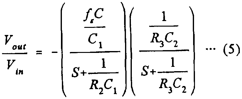
qui est semblable à l'équation (1). which is similar to equation (1).
En outre, le filtre passe-bas 40 fonctionne de la même manière que le filtre passe-bas 20. Sur la figure 5, +1 et 2 sont des signaux d'horloge de commutation complémentaires appliqués aux gâchettes des commutateurs analogiques. In addition, the low pass filter 40 operates in the same manner as the low pass filter 20. In Fig. 5, +1 and 2 are complementary switching clock signals applied to the gates of the analog switches.
De même, si la méthode des capacités commutées mentionnée ci-dessus est appliquée dans le cas d'entrées différentielles, le filtre passe-bas 40 devient un filtre passe-bas 60 représenté sur la figure 6. La capacité C' des condensateurs utilisés dans le filtre passe-bas 60 représente un quart de la capacité C du condensateur utilisé dans le filtre passe-bas 40 (c'est-à-dire que C' = C/4). Comme on peut le voir à partir des figures 5 et 6, la surface de puce nécessaire pour le filtre passe-bas 60 peut être pratiquement identique à celle requise pour le filtre passe-bas 50. De plus, le fonctionnement du filtre passe-bas 60 est le même que celui du filtre passe-bas 20. Similarly, if the switched capacitance method mentioned above is applied in the case of differential inputs, the low-pass filter 40 becomes a low-pass filter 60 shown in FIG. 6. The capacitor C 'of the capacitors used in FIG. the low-pass filter 60 represents one-quarter of the capacitance C of the capacitor used in the low-pass filter 40 (i.e., C '= C / 4). As can be seen from FIGS. 5 and 6, the chip area required for the low-pass filter 60 may be substantially the same as that required for the low-pass filter 50. In addition, the operation of the low-pass filter 60 is the same as that of the low-pass filter 20.
La description détaillée du mode de réalisation préféré de la présente invention va être poursuivie en référence au principe décrit ci-dessus de la présente invention et à la figure 7. The detailed description of the preferred embodiment of the present invention will be continued with reference to the above-described principle of the present invention and to FIG.
La figure 7 est un schéma de circuit d'un filtre passe-bas analogique selon la présente invention destiné à convertir des entrées différentielles en une sortie asynchrone. Comme cela est visible sur la figure 7, un filtre passe-bas 70 comprend des premier et second moyens de charge/décharge de signaux analogiques 1 et 2 destinés à recevoir des signaux analogiques différentiels Vinp et Vinn et à charger et/ou décharger des condensateurs, un amplificateur opérationnel à entrées différentielles et à sortie asynchrone 4 destiné à amplifier la différence entre ses bornes d'entrée. La borne d'entrée négative (-) de l'amplificateur opérationnel 4 est reliée à la borne de sortie commune des moyens de charge/décharge de signaux analogiques 1 et 2, tandis que sa borne d'entrée positive (+) est reliée à la masse. En outre, un moyen de commande de gain et de génération de pôle 3 est monté entre la borne d'entrée négative et la borne de sortie de l'amplificateur opérationnel 4 pour commander le gain de ce dernier, et pour générer le pôle de la fonction de transfert de l'amplificateur opérationnel 4, et un moyen de filtrage passe-bas 5 est monté entre la borne de sortie de l'amplificateur opérationnel 4 et la borne de sortie asymétrique finale Vout pour filtrer le signal de sortie de l'amplificateur opérationnel 4. Fig. 7 is a circuit diagram of an analog low pass filter according to the present invention for converting differential inputs to an asynchronous output. As can be seen in FIG. 7, a low-pass filter 70 comprises first and second analog signal load / discharge means 1 and 2 for receiving differential analog signals Vinp and Vinn and for charging and / or discharging capacitors. an operational amplifier with differential inputs and asynchronous output 4 for amplifying the difference between its input terminals. The negative input terminal (-) of the operational amplifier 4 is connected to the common output terminal of the analog signal charging / discharging means 1 and 2, while its positive (+) input terminal is connected to the mass. Further, gain control and pole generating means 3 are connected between the negative input terminal and the output terminal of the operational amplifier 4 to control the gain thereof, and to generate the pole of the transfer function of the operational amplifier 4, and a low-pass filtering means 5 is connected between the output terminal of the operational amplifier 4 and the final unbalanced output terminal Vout for filtering the output signal of the amplifier operational 4.
Les premiers moyens de charge/décharge de signal analogique chargent des premiers et second condensateurs
Cinpl et Cinp2 pendant qu'ils reçoivent le signal d'entrée analogique Vinp et déchargent les condensateurs Cinpl et
Cinp2 sur la borne d'entrée négative de l'amplificateur opérationnel 4. De même, les seconds moyens de charge/décharge de signal analogique chargent des troisième et quatrième condensateurs Cinnl et Cinn2 pendant qu'ils reçoivent le signal d'entrée analogique Vinn et déchargent les condensateurs Cinnl et Cinn2 sur la borne d'entrée négative de l'amplificateur opérationnel 4.The first analog signal charging / discharging means charge first and second capacitors
Cinpl and Cinp2 as they receive the Vinp analog input signal and discharge the Cinpl capacitors and
Cinp2 on the negative input terminal of the operational amplifier 4. Similarly, the second analog signal charging / discharging means charge third and fourth capacitors Cinn1 and Cinn2 as they receive the analog input signal Vinn and discharge the capacitors Cinn1 and Cinn2 on the negative input terminal of the operational amplifier 4.
Les premiers moyens de charge/décharge de signal analogique 1 comprennent des première et seconde unités de charge/décharge 11 et 12 respectivement destinées à charger le signal d'entrée analogique Vinp dans les condensateurs
Cinpl et Cinp2 et/ou à le décharger de ceux-ci en réponse à l'action de commutateurs SW1 à SW8, chacune des unités de charge/décharge 11 et 12 comprenant 4 commutateurs analogiques et un condensateur.The first analog signal charging / discharging means 1 comprise first and second charge / discharge units 11 and 12 respectively for charging the analog input signal Vinp in the capacitors.
Cinpl and Cinp2 and / or discharge thereof in response to the action of switches SW1 to SW8, each of the charging / discharging units 11 and 12 comprising 4 analog switches and a capacitor.
La première unité de charge/décharge 11 comprend un premier commutateur SW1 relié à une borne d'entrée pour commuter le signal d'entrée Vinp, le premier condensateur
Cinpl relié au premier commutateur SW1, un second-commutateur
SW2 relié au premier condensateur Cinpl et à la borne d'entrée négative de l'amplificateur opérationnel 4, un troisième commutateur SW3 relié au premier condensateur Cinpl et à la masse, et un quatrième commutateur SW4 relié au premier condensateur Cinpl et à la masse.The first charge / discharge unit 11 comprises a first switch SW1 connected to an input terminal for switching the input signal Vinp, the first capacitor
Cinpl connected to the first switch SW1, a second-switch
SW2 connected to the first capacitor Cinpl and to the negative input terminal of the operational amplifier 4, a third switch SW3 connected to the first capacitor Cinp1 and to the ground, and a fourth switch SW4 connected to the first capacitor Cinp1 and grounded.
La seconde unité de charge/décharge 12 comprend un cinquième commutateur SW5 relié à la borne d'entrée pour commuter le signal d'entrée Vinp, le second condensateur
Cinp2 relié au cinquième commutateur SW5, un sixième commutateur SW6 relié au second condensateur Cinp2 et à la borne d'entrée négative de l'amplificateur opérationnel 4, un septième commutateur SW7 relié au second condensateur Cinp2 et à la masse, et un huitième commutateur SW8 relié au second condensateur Cinp2 et à la masse.The second charge / discharge unit 12 comprises a fifth switch SW5 connected to the input terminal for switching the input signal Vinp, the second capacitor
Cinp2 connected to the fifth switch SW5, a sixth switch SW6 connected to the second capacitor Cinp2 and to the negative input terminal of the operational amplifier 4, a seventh switch SW7 connected to the second capacitor Cinp2 and to the ground, and an eighth switch SW8 connected to the second capacitor Cinp2 and to ground.
D'autre part, les seconds moyens de charge/décharge de signal analogique 2 comprennent des troisième et quatrième unités de charge/décharge 21 et 22 respectivement destinées à charger le signal d'entrée analogique Vinn dans les condensateurs Cinnl et Cinn2 et à le décharger de ceux-ci en réponse à l'action de commutateurs SW9 à SW16, chacune des troisième et quatrième unités de charge/décharge 21 et 22 comprenant 4 commutateurs analogiques et un condensateur. On the other hand, the second analog signal charging / discharging means 2 comprise third and fourth charge / discharge units 21 and 22 respectively for charging the analog input signal Vinn in the Cinn1 and Cinn2 capacitors and for discharging it. of these in response to the action of switches SW9 to SW16, each of the third and fourth charge / discharge units 21 and 22 comprising 4 analog switches and a capacitor.
La troisième unité de charge/décharge 21 comprend un neuvième commutateur SW9 relié à une autre borne d'entrée pour commuter le signal d'entrée Vinn, un dixième commutateur SW10 relié au neuvième commutateur SW9 et à la borne d'entrée négative de l'amplificateur opérationnel 4, le troisième condensateur Cinnl relié à un noeud situé entre les neuvième et dixième commutateurs SW9 et SW10, un onzième commutateur
SW11 relié au troisième condensateur Cinnl et à la masse, et un douzième commutateur SW12 également relié au troisième condensateur Cinnl et à la masse.The third charge / discharge unit 21 comprises a ninth switch SW9 connected to another input terminal for switching the input signal Vinn, a tenth switch SW10 connected to the ninth switch SW9 and to the negative input terminal of the operational amplifier 4, the third capacitor Cinnl connected to a node located between the ninth and tenth switches SW9 and SW10, an eleventh switch
SW11 connected to the third capacitor Cinnl and ground, and a twelfth switch SW12 also connected to the third capacitor Cinnl and grounded.
La quatrième unité de charge/décharge 22 comprend un troisième commutateur SW13 relié à l'autre borne d'entrée pour commuter le signal d'entrée Vinn, un quatrième commutateur SW14 relié au treizième commutateur SW13 et à la borne d'entrée négative de l'amplificateur opérationnel 4, le quatrième condensateur Cinn2 relié à un noeud situé entre les treizième et quatorzième commutateurs SW13 et SW14, un quinzième commutateur SW15 relié au quatrième condensateur
Cinn2 et à la masse, et un seizième commutateur SW16 également relié au quatrième condensateur Cinn2 et à la masse.The fourth charge / discharge unit 22 comprises a third switch SW13 connected to the other input terminal for switching the input signal Vinn, a fourth switch SW14 connected to the thirteenth switch SW13 and to the negative input terminal of the operational amplifier 4, the fourth capacitor Cinn2 connected to a node situated between the thirteenth and fourteenth switches SW13 and SW14, a fifteenth switch SW15 connected to the fourth capacitor
Cinn2 and ground, and a sixteenth SW16 switch also connected to the fourth capacitor Cinn2 and ground.
Les commutateurs SW1 à SW16 sont groupés en quatre groupes qui reçoivent quatre signaux d'horloge déphasés, les fréquences communes des signaux d'horloge étant fs. Les commutateurs SW1 à SW16 chargent et/ou déchargent les condensateurs Cinpl, Cinp2, Cinnl et Cinn2 en réponse à ces signaux d'horloge, comme cela sera décrit ci-après. The switches SW1 to SW16 are grouped into four groups which receive four out of phase clock signals, the common frequencies of the clock signals being fs. The switches SW1 to SW16 charge and / or discharge the capacitors Cinpl, Cinp2, Cinn1 and Cinn2 in response to these clock signals, as will be described hereinafter.
Les opérations de commutation des commutateurs SW1 à SW16 vont maintenant être décrites en détail en référence à la figure 8. La figure 8 est un chronogramme des signaux d'horloge appliqués aux commutateurs SW1 à SW16. Lorsque le signal est "haut", le commutateur auquel le signal est appliqué est passant, tandis que lorsque le signal est "bas", le commutateur est non passant. The switching operations of the switches SW1 to SW16 will now be described in detail with reference to Fig. 8. Fig. 8 is a timing chart of the clock signals applied to the switches SW1 to SW16. When the signal is "high", the switch to which the signal is applied is on, whereas when the signal is "low", the switch is off.
Comme cela est visible sur la figure 7, les commutateurs SW4, SW6, SW10 et SW16 reçoivent un premier signal d'horloge les commutateurs SWl, SW7, SW11 et SW13 reçoivent un premier signal d'horloge retardé #1d, les commutateurs SW2,
SW8, SW12 et SW14 reçoivent un second signal d'horloge 2 et les commutateurs SW3, SW5, SW9 et SW15 reçoivent un second signal d'horloge retardé +2d. En outre, comme cela est visible sur la figure 8, le premier signal d'horloge +1 et le second signal d'horloge sont déphasés d'environ 180 degrés. As can be seen in FIG. 7, the switches SW4, SW6, SW10 and SW16 receive a first clock signal. The switches SW1, SW7, SW11 and SW13 receive a first delayed clock signal # 1d, the switches SW2,
SW8, SW12 and SW14 receive a second clock signal 2 and the switches SW3, SW5, SW9 and SW15 receive a second delayed clock signal + 2d. Furthermore, as can be seen in FIG. 8, the first +1 clock signal and the second clock signal are out of phase by about 180 degrees.
Autrement dit, lorsqu'un signal est "haut", l'autre est "bas", et vice versa.In other words, when one signal is "high", the other is "low", and vice versa.
Lorsque le premier signal d'horloge 1 et le premier signal d'horloge retardé Qld deviennent successivement "hauts", les commutateurs SW1 et SW4 de la première unité de charge/décharge 11 sont rendus passants de sorte que la tension d'entrée Vinp est transférée pour charger le premier condensateur Cinpl, et les commutateurs SW6 et SW7 de la seconde unité de charge/décharge 12 sont rendus passants de sorte que la tension Vinp chargée précédemment du second condensateur Cinp2 est déchargée et transférée à la borne d'entrée négative de l'amplificateur opérationnel 4. When the first clock signal 1 and the first delayed clock signal Q 1 become "high" successively, the switches SW 1 and SW 4 of the first charge / discharge unit 11 are turned on so that the input voltage Vin p is transferred to charge the first capacitor Cinpl, and the switches SW6 and SW7 of the second charge / discharge unit 12 are turned on so that the previously charged voltage Vinp of the second capacitor Cinp2 is discharged and transferred to the negative input terminal of the operational amplifier 4.
Puis, après que le premier signal d'horloge 1 et le premier signal d'horloge retardé fld sont devenus successivement "bas" et lorsque le second signal d'horloge 2 et le second signal d'horloge retardé 2d deviennent successivement "hauts", les commutateurs SW2 et SW3 de la première unité de charge/décharge 11 sont rendus passants de sorte que la tension Vinp chargée précédemment du premier condensateur Cinpl est déchargée et transférée à la borne d'entrée négative de l'amplificateur opérationnel 4. De plus, les commutateurs SW5 et SW8 de la seconde unité de charge/décharge 12 sont rendus passants de sorte que la tension d'entrée Vinp est transférée pour charger le second condensateur Cinp2. Then, after the first clock signal 1 and the first delayed clock signal fld have successively become "low" and when the second clock signal 2 and the second delayed clock signal 2d successively become "high", the switches SW2 and SW3 of the first charge / discharge unit 11 are turned on so that the previously charged voltage Vinp of the first capacitor Cinp1 is discharged and transferred to the negative input terminal of the operational amplifier 4. the switches SW5 and SW8 of the second charge / discharge unit 12 are turned on so that the input voltage Vinp is transferred to charge the second capacitor Cinp2.
Comme cela a été décrit précédemment, étant donné que les moyens de charge/décharge 1 ou 2 chargent et déchargent le condensateur au cours d'un seul cycle d'horloge, le filtre passe-bas 70 de la présente invention réalise une double opération d'échantillonnage. As previously described, since the charging / discharging means 1 or 2 charge and discharge the capacitor in a single clock cycle, the low pass filter 70 of the present invention performs a dual operation of 'sampling.
De même, lorsque le premier signal d'horloge 1 et le premier signal d'horloge retardé Qld deviennent successivement "hauts", les commutateurs SW10 et SW11 de la troisième unité de charge/décharge 21 sont rendus passants de sorte que la tension Vinn chargée précédemment du troisième condensateur
Cinnl est déchargée et transférée à la borne d'entrée négative de l'amplificateur opérationnel 4, et les commutateurs SW13 et SW16 de la quatrième unité de charge/décharge 22 sont rendus passants de sorte que la tension d'entrée Vinn est transférée pour charger le quatrième condensateur Cinn2.Similarly, when the first clock signal 1 and the first delayed clock signal Qld become "high" successively, the switches SW10 and SW11 of the third charge / discharge unit 21 are turned on so that the voltage Vinn loaded previously of the third capacitor
Cinn1 is discharged and transferred to the negative input terminal of the operational amplifier 4, and the switches SW13 and SW16 of the fourth charge / discharge unit 22 are turned on so that the input voltage Vinn is transferred to charge. the fourth Cinn2 capacitor.
Puis, après que le premier signal d'horloge 1 et le premier signal d'horloge retardé Qld sont devenus successivement "bas" et lorsque le second signal d'horloge +2 et le second signal d'horloge retardé fid deviennent successivement "hauts", les commutateurs SW9 et SWl2 de la troisième unité de charge/décharge 21 sont rendus passants de sorte que la tension d'entrée Vinn est transférée pour charger le troisième condensateur Cinnl, et les commutateurs SW14 et SW15 de la quatrième unité de charge/décharge 22 sont rendus passants de sorte que la tension Vinn chargée précédemment du condensateur Cinn2 est déchargée et transférée à la borne d'entrée négative de l'amplificateur opérationnel 4. Ceci assure également la double opération d'échantillonnage. Then, after the first clock signal 1 and the first delayed clock signal Qld have successively become "low" and when the second clock signal +2 and the second delayed clock signal fid become successively "high" the switches SW9 and SW12 of the third charge / discharge unit 21 are turned on so that the input voltage Vinn is transferred to charge the third capacitor Cinn1, and the switches SW14 and SW15 of the fourth charge / discharge unit. 22 are turned on so that the voltage Vinn previously loaded capacitor Cinn2 is discharged and transferred to the negative input terminal of the operational amplifier 4. This also ensures the double sampling operation.
Pendant que le second signal d'horloge 2 et le second signal d'horloge retardé 2d sont "hauts", la quantité de charges transférées des unités de charge/décharge 11 et 22 à la borne d'entrée négative de l'amplificateur opérationnel 4 est donnée par l'équation suivante:
C(Vinp - Vinn)/4 = 2Vinp ' C/4 ou -2Vinn ' C/4 ...(6) dans laquelle Vinp = -Vinn A Vin ... (3).While the second clock signal 2 and the second delayed clock signal 2d are "high", the amount of charges transferred from the charging / discharging units 11 and 22 to the negative input terminal of the operational amplifier 4 is given by the following equation:
C (Vinp - Vinn) / 4 = 2Vinp 'C / 4 or -2Vinn' C / 4 ... (6) in which Vinp = -Vinn A Vin ... (3).
D'autre part, pendant que le premier signal d'horloge Xl et le premier signal d'horloge retardé 4 > ld sont "hauts", la quantité de charges transférées des unités de charge/décharge 12 et 21 à la borne d'entrée négative de l'amplificateur opérationnel 4 est donnée par l'équation suivante:
C(Vinp - Vinn)/4 = 2Vinp ' C/4 ou -2Vinn e C/4 ...(7)
dans laquelle Vinp = -Vinn A Vin ... (3).On the other hand, while the first clock signal X1 and the first delayed clock signal 4> 1d are "high", the amount of charges transferred from the charging / discharging units 12 and 21 to the input terminal negative of the operational amplifier 4 is given by the following equation:
C (Vinp - Vinn) / 4 = 2Vinp 'C / 4 or -2Vinn e C / 4 ... (7)
in which Vinp = -Vinn A Vin ... (3).
Par conséquent, la quantité totale de charges transférées à la borne d'entrée négative de l'amplificateur opérationnel 4 est la suivante:
Equation (6) + Equation (7) = 4Vinp ' C/4 = Vinp ' C
(8)
Comme cela a été décrit précédemment, étant donné que la capacité de chacun des condensateurs Cinpl, Cinp2, Cinnl et
Cinn2 est de C/4, le gain devient égal à 1/4 de la valeur initiale avec davantage de précision.Therefore, the total amount of charges transferred to the negative input terminal of the operational amplifier 4 is as follows:
Equation (6) + Equation (7) = 4Vinp 'C / 4 = Vinp' C
(8)
As has been previously described, since the capacitance of each of the capacitors Cinpl, Cinp2, Cinnl and
Cinn2 is C / 4, the gain becomes equal to 1/4 of the initial value with more precision.
Le moyen de commande de gain et de génération de pôle 3 comprend une résistance passive R2 montée entre la borne d'entrée négative et la borne de sortie de l'amplificateur opérationnel 4, et un condensateur C1 monté en parallèle à la résistance R2. Le moyen de commande de gain et de génération de pôle 3 joue le rôle d'un premier filtre passe-bas ayant une fréquence de coupure f3dB de:
- 2 gC (9)
2R2C1
En outre, le gain de tension K du moyen de commande de gain et de génération de pôle 3 est le suivant:

- 2 gC (9)
2R2C1
In addition, the voltage gain K of the gain control and pole generation means 3 is as follows:
L'amplificateur opérationnel à entrée différentielle et sortie asymétrique 4 comprend des bornes d'entrée négative et positive, la borne d'entrée positive étant reliée à la masse de sorte que la différence des deux signaux d'entrée est amplifiée et délivrée en sortie à partir de la borne de sortie. The operational amplifier with differential input and asymmetric output 4 comprises negative and positive input terminals, the positive input terminal being connected to ground so that the difference of the two input signals is amplified and outputted to from the output terminal.
Le moyen de filtrage passe-bas 5 comprend une résistance passive R3 montée entre la borne de sortie de l'amplificateur opérationnel 4 et la borne de sortie finale Vout du filtre passe-bas 70, et un condensateur C2 monté entre la borne de sortie finale Vout et la masse. Le moyen de filtrage passebas 5 joue le rôle d'un second filtre passe-bas ayant une fréquence de coupure f3dB de:
(11)
= 2itR3Q
En outre, le gain de tension K du moyen de filtrage passe-bas 5 est exprimé par l'équation suivante:
K = 1 . .. (12)
Le signal filtré par le moyen de filtrage passe-bas 5 est fourni en sortie sous la forme d'un signal de sortie analogique à partir de la borne de sortie finale Vout.The low-pass filtering means 5 comprises a passive resistor R3 mounted between the output terminal of the operational amplifier 4 and the final output terminal Vout of the low-pass filter 70, and a capacitor C2 connected between the final output terminal. Vout and the mass. The lowpass filtering means 5 acts as a second lowpass filter having a cutoff frequency f3dB of:
(11)
= 2itR3Q
In addition, the voltage gain K of the low-pass filtering means 5 is expressed by the following equation:
K = 1. .. (12)
The signal filtered by the low-pass filtering means 5 is output as an analog output signal from the final output terminal Vout.
Comme cela a été décrit précédemment, le filtre passebas 70 de la présente invention joue le rôle d'un filtre passe-bas analogique à double échantillonnage secondaire. As previously described, the low pass filter 70 of the present invention acts as a secondary double sampling analog low pass filter.
Cependant, le filtre passe-bas 70 peut également être conçu pour jouer le rôle d'un filtre passe-bas d'étage supérieur.However, the low-pass filter 70 may also be designed to act as a high-pass low-pass filter.
En outre, le filtre passe-bas 70 de la présente invention peut s'appliquer à un convertisseur numérique-analogique audio ou à un circuit intégré de communication vocale dans lequel un traitement de haute précision du signal analogique est nécessaire et dans lequel la distorsion harmonique totale (THD) doit être inférieure à 0,01%. La surface de puce nécessaire à la mise en oeuvre du filtre passe-bas analogique à double échantillonnage de l'invention est moins importante et l'appariement des condensateurs est plus facile que dans le filtre passe-bas conventionnel. In addition, the low-pass filter 70 of the present invention can be applied to a digital to analog audio converter or to an integrated speech communication circuit in which a high precision processing of the analog signal is required and in which the harmonic distortion total (THD) should be less than 0.01%. The chip area necessary for implementing the analog double-pass low-pass filter of the invention is smaller and capacitor pairing is easier than in the conventional low-pass filter.
Bien que la description précédente ait porté sur un mode de réalisation préféré de l'invention, celle-ci n'est bien entendu pas limitée à l'exemple particulier décrit et illustré ici et l'homme de l'art comprendra aisément qu'il est possible d'y apporter de nombreuses variantes et modifications sans pour autant sortir du cadre de l'invention. Although the foregoing description has dealt with a preferred embodiment of the invention, this is of course not limited to the particular example described and illustrated here and those skilled in the art will readily understand that It is possible to make many variations and modifications without departing from the scope of the invention.
Claims (8)
Applications Claiming Priority (1)
| Application Number | Priority Date | Filing Date | Title |
|---|---|---|---|
| KR1019970029634A KR100256251B1 (en) | 1997-06-30 | 1997-06-30 | Dual sampling analog low pass filter |
Publications (2)
| Publication Number | Publication Date |
|---|---|
| FR2765417A1 true FR2765417A1 (en) | 1998-12-31 |
| FR2765417B1 FR2765417B1 (en) | 2000-10-20 |
Family
ID=19512594
Family Applications (1)
| Application Number | Title | Priority Date | Filing Date |
|---|---|---|---|
| FR9808317A Expired - Lifetime FR2765417B1 (en) | 1997-06-30 | 1998-06-30 | ANALOG DOUBLE SAMPLING LOW PASS FILTER |
Country Status (4)
| Country | Link |
|---|---|
| US (1) | US6107871A (en) |
| JP (1) | JP3128647B2 (en) |
| KR (1) | KR100256251B1 (en) |
| FR (1) | FR2765417B1 (en) |
Cited By (1)
| Publication number | Priority date | Publication date | Assignee | Title |
|---|---|---|---|---|
| US6636406B1 (en) | 1997-04-08 | 2003-10-21 | X2Y Attenuators, Llc | Universal multi-functional common conductive shield structure for electrical circuitry and energy conditioning |
Families Citing this family (25)
| Publication number | Priority date | Publication date | Assignee | Title |
|---|---|---|---|---|
| US9054094B2 (en) | 1997-04-08 | 2015-06-09 | X2Y Attenuators, Llc | Energy conditioning circuit arrangement for integrated circuit |
| US7336468B2 (en) | 1997-04-08 | 2008-02-26 | X2Y Attenuators, Llc | Arrangement for energy conditioning |
| US7301748B2 (en) | 1997-04-08 | 2007-11-27 | Anthony Anthony A | Universal energy conditioning interposer with circuit architecture |
| US7321485B2 (en) | 1997-04-08 | 2008-01-22 | X2Y Attenuators, Llc | Arrangement for energy conditioning |
| US6549066B1 (en) * | 2001-08-21 | 2003-04-15 | National Semiconductor Corporation | Efficient implementation of a complex filter with on chip resistor tuning |
| KR20060120683A (en) | 2003-12-22 | 2006-11-27 | 엑스2와이 어테뉴에이터스, 엘.엘.씨 | Internally shielded energy conditioner |
| US7315200B2 (en) * | 2004-03-31 | 2008-01-01 | Silicon Labs Cp, Inc. | Gain control for delta sigma analog-to-digital converter |
| US7630188B2 (en) | 2005-03-01 | 2009-12-08 | X2Y Attenuators, Llc | Conditioner with coplanar conductors |
| US7817397B2 (en) | 2005-03-01 | 2010-10-19 | X2Y Attenuators, Llc | Energy conditioner with tied through electrodes |
| TWI257767B (en) * | 2005-03-03 | 2006-07-01 | Realtek Semiconductor Corp | Filtering device having multiple inputs and multiple feedback paths |
| US7414555B1 (en) * | 2005-09-16 | 2008-08-19 | Atheros Communications, Inc. | Interleaved ADC and folded mixer for WLAN devices |
| JP2007151100A (en) * | 2005-10-31 | 2007-06-14 | Sanyo Electric Co Ltd | Sample and hold circuit |
| CN101395683A (en) | 2006-03-07 | 2009-03-25 | X2Y衰减器有限公司 | Energy conditioner structures |
| JP2008035451A (en) * | 2006-08-01 | 2008-02-14 | Niigata Seimitsu Kk | Frequency synthesizer and loop filter therefor |
| US7990209B2 (en) * | 2009-06-19 | 2011-08-02 | Allegro Microsystems, Inc. | Switched capacitor notch filter |
| US8035436B2 (en) * | 2009-09-24 | 2011-10-11 | Oracle America, Inc. | Passive capacitively injected phase interpolator |
| KR101283468B1 (en) * | 2009-11-19 | 2013-07-23 | 한국전자통신연구원 | Loop filter and phase locked loop comprising the same |
| JP4729658B2 (en) * | 2009-12-21 | 2011-07-20 | オンキヨー株式会社 | Filter circuit |
| US8416014B2 (en) * | 2010-03-12 | 2013-04-09 | Allegro Microsystems, Inc. | Switched capacitor notch filter with fast response time |
| KR101019159B1 (en) * | 2010-09-17 | 2011-03-03 | 주식회사 룩센테크놀러지 | Signal sampling circuit having improved noise characteristics and image sensor using the same |
| US8508257B2 (en) * | 2011-04-28 | 2013-08-13 | Analog Devices, Inc. | Noise cancellation system and method for amplifiers |
| US8427217B1 (en) * | 2012-03-29 | 2013-04-23 | Panasonic Corporation | Phase interpolator based on an injected passive RLC resonator |
| US9496889B2 (en) * | 2014-10-13 | 2016-11-15 | Nxp B.V. | Direct sigma-delta receiver |
| CN106208679A (en) * | 2016-07-15 | 2016-12-07 | 武汉华星光电技术有限公司 | A kind of voltage conversion circuit and liquid crystal display drive chip |
| JP6753330B2 (en) * | 2017-02-15 | 2020-09-09 | 株式会社デンソー | Delta-sigma modulator, ΔΣA / D converter and incremental ΔΣA / D converter |
Citations (2)
| Publication number | Priority date | Publication date | Assignee | Title |
|---|---|---|---|---|
| EP0080234A1 (en) * | 1981-11-20 | 1983-06-01 | Koninklijke Philips Electronics N.V. | Filter circuit incorporating a differential amplifier |
| JPH01321716A (en) * | 1988-06-23 | 1989-12-27 | Nec Corp | Active filter |
Family Cites Families (3)
| Publication number | Priority date | Publication date | Assignee | Title |
|---|---|---|---|---|
| JPH0783510B2 (en) * | 1986-08-26 | 1995-09-06 | 松下電工株式会社 | Centralized monitoring controller |
| EP0433032A3 (en) * | 1989-12-15 | 1992-08-05 | Matsushita Electric Industrial Co., Ltd. | Signal reproducing apparatus |
| US5341050A (en) * | 1992-03-20 | 1994-08-23 | Hughes Aircraft Company | Switched capacitor amplifier circuit operating without serially coupled amplifiers |
-
1997
- 1997-06-30 KR KR1019970029634A patent/KR100256251B1/en not_active IP Right Cessation
-
1998
- 1998-06-29 US US09/106,262 patent/US6107871A/en not_active Expired - Lifetime
- 1998-06-30 FR FR9808317A patent/FR2765417B1/en not_active Expired - Lifetime
- 1998-06-30 JP JP10185177A patent/JP3128647B2/en not_active Expired - Lifetime
Patent Citations (2)
| Publication number | Priority date | Publication date | Assignee | Title |
|---|---|---|---|---|
| EP0080234A1 (en) * | 1981-11-20 | 1983-06-01 | Koninklijke Philips Electronics N.V. | Filter circuit incorporating a differential amplifier |
| JPH01321716A (en) * | 1988-06-23 | 1989-12-27 | Nec Corp | Active filter |
Non-Patent Citations (3)
| Title |
|---|
| JACOB MILLMAN ET AL.: "Microelectronics", 1988, MCGRAW-HILL, SINGAPORE, XP002122691 * |
| MOHAMED ISMAIL: "New Fully-Integrated Mosfet-Capacitor Active Filters", PROCEEDINGS OF THE INTERNATIONAL SYMPOSIUM ON CIRCUITS AND SYSTEMS, June 1985 (1985-06-01), New York, US, pages 1435 - 1438, XP002122690 * |
| PATENT ABSTRACTS OF JAPAN vol. 014, no. 130 (E - 0901) 12 March 1990 (1990-03-12) * |
Cited By (1)
| Publication number | Priority date | Publication date | Assignee | Title |
|---|---|---|---|---|
| US6636406B1 (en) | 1997-04-08 | 2003-10-21 | X2Y Attenuators, Llc | Universal multi-functional common conductive shield structure for electrical circuitry and energy conditioning |
Also Published As
| Publication number | Publication date |
|---|---|
| JP3128647B2 (en) | 2001-01-29 |
| KR19990005437A (en) | 1999-01-25 |
| KR100256251B1 (en) | 2000-05-15 |
| JPH11168353A (en) | 1999-06-22 |
| US6107871A (en) | 2000-08-22 |
| FR2765417B1 (en) | 2000-10-20 |
Similar Documents
| Publication | Publication Date | Title |
|---|---|---|
| FR2765417A1 (en) | Analog low-pass filter with double sampling | |
| JP3621385B2 (en) | Switched capacitor amplifier and analog interface circuit for charge coupled device using the same | |
| US5892473A (en) | Switched capacitor digital-analog converter with a decreased harmonic distortion | |
| EP1317068B1 (en) | Incremental-delta analogue to digital conversion | |
| TWI246826B (en) | High precision analog to digital converter | |
| US4851841A (en) | Gain scaling of oversampled analog-to-digital converters | |
| EP1646147A1 (en) | Analog filter for time discrete signals based on passive components | |
| US20110102223A1 (en) | Amplifier with digital input and digital pwm control loop | |
| WO1994023494A1 (en) | Double sampled biquad switched capacitor filter | |
| WO2004095512A2 (en) | Sample and hold circuits and methods with offset error correction and systems using the same | |
| US7936297B2 (en) | Analog to digital converter | |
| KR100285933B1 (en) | Full differential analogue circuit | |
| JPS618800A (en) | 2-hierarchical sample holding circuit | |
| EP1076874B1 (en) | Method and circuit for compensating the non-linearity of capacitors | |
| EP2131494B1 (en) | Circuit with switched capacitances with reduced consumption | |
| US11876539B2 (en) | Current to digital converter circuit, optical front end circuit, computed tomography apparatus and method | |
| US20020140591A1 (en) | Sigma-delta A/D converter | |
| AU7161900A (en) | Transducer interface arrangement including a sigma-delta modulator with offset correction and with gain setting | |
| JP2000174572A (en) | Voltage amplifier | |
| FR2769773A1 (en) | ANALOG-TO-DIGITAL CONVERSION DEVICE | |
| JPH04243326A (en) | Oversampling d/a converter | |
| FR2662033A1 (en) | Analog-digital conversion circuit of algorithmic type | |
| FR2712413A1 (en) | Method and apparatus for integrating a plurality of input signals. | |
| US20090015452A1 (en) | Method and Device for Analong Digital Conversion of a Complex Signal | |
| EP0308287B1 (en) | Switched capacitor biquadratic element without a permanent negative feedback loop and having a low sensitivity towards operational amplifier gain and capacitor ratio |
Legal Events
| Date | Code | Title | Description |
|---|---|---|---|
| CA | Change of address | ||
| CD | Change of name or company name | ||
| TP | Transmission of property | ||
| PLFP | Fee payment |
Year of fee payment: 19 |
|
| PLFP | Fee payment |
Year of fee payment: 20 |