EP4583130A1 - Structural body and structural body manufacturing method - Google Patents
Structural body and structural body manufacturing method Download PDFInfo
- Publication number
- EP4583130A1 EP4583130A1 EP23859879.1A EP23859879A EP4583130A1 EP 4583130 A1 EP4583130 A1 EP 4583130A1 EP 23859879 A EP23859879 A EP 23859879A EP 4583130 A1 EP4583130 A1 EP 4583130A1
- Authority
- EP
- European Patent Office
- Prior art keywords
- magnetic body
- body portion
- magnetic
- planar inductor
- insulating layer
- Prior art date
- Legal status (The legal status is an assumption and is not a legal conclusion. Google has not performed a legal analysis and makes no representation as to the accuracy of the status listed.)
- Pending
Links
Images




Classifications
-
- H—ELECTRICITY
- H01—ELECTRIC ELEMENTS
- H01F—MAGNETS; INDUCTANCES; TRANSFORMERS; SELECTION OF MATERIALS FOR THEIR MAGNETIC PROPERTIES
- H01F1/00—Magnets or magnetic bodies characterised by the magnetic materials therefor; Selection of materials for their magnetic properties
- H01F1/01—Magnets or magnetic bodies characterised by the magnetic materials therefor; Selection of materials for their magnetic properties of inorganic materials
- H01F1/03—Magnets or magnetic bodies characterised by the magnetic materials therefor; Selection of materials for their magnetic properties of inorganic materials characterised by their coercivity
- H01F1/12—Magnets or magnetic bodies characterised by the magnetic materials therefor; Selection of materials for their magnetic properties of inorganic materials characterised by their coercivity of soft-magnetic materials
- H01F1/14—Magnets or magnetic bodies characterised by the magnetic materials therefor; Selection of materials for their magnetic properties of inorganic materials characterised by their coercivity of soft-magnetic materials metals or alloys
- H01F1/20—Magnets or magnetic bodies characterised by the magnetic materials therefor; Selection of materials for their magnetic properties of inorganic materials characterised by their coercivity of soft-magnetic materials metals or alloys in the form of particles, e.g. powder
- H01F1/22—Magnets or magnetic bodies characterised by the magnetic materials therefor; Selection of materials for their magnetic properties of inorganic materials characterised by their coercivity of soft-magnetic materials metals or alloys in the form of particles, e.g. powder pressed, sintered, or bound together
-
- H—ELECTRICITY
- H01—ELECTRIC ELEMENTS
- H01F—MAGNETS; INDUCTANCES; TRANSFORMERS; SELECTION OF MATERIALS FOR THEIR MAGNETIC PROPERTIES
- H01F27/00—Details of transformers or inductances, in general
- H01F27/28—Coils; Windings; Conductive connections
- H01F27/32—Insulating of coils, windings, or parts thereof
- H01F27/323—Insulation between winding turns, between winding layers
-
- H—ELECTRICITY
- H01—ELECTRIC ELEMENTS
- H01F—MAGNETS; INDUCTANCES; TRANSFORMERS; SELECTION OF MATERIALS FOR THEIR MAGNETIC PROPERTIES
- H01F1/00—Magnets or magnetic bodies characterised by the magnetic materials therefor; Selection of materials for their magnetic properties
- H01F1/01—Magnets or magnetic bodies characterised by the magnetic materials therefor; Selection of materials for their magnetic properties of inorganic materials
- H01F1/03—Magnets or magnetic bodies characterised by the magnetic materials therefor; Selection of materials for their magnetic properties of inorganic materials characterised by their coercivity
- H01F1/12—Magnets or magnetic bodies characterised by the magnetic materials therefor; Selection of materials for their magnetic properties of inorganic materials characterised by their coercivity of soft-magnetic materials
- H01F1/14—Magnets or magnetic bodies characterised by the magnetic materials therefor; Selection of materials for their magnetic properties of inorganic materials characterised by their coercivity of soft-magnetic materials metals or alloys
- H01F1/20—Magnets or magnetic bodies characterised by the magnetic materials therefor; Selection of materials for their magnetic properties of inorganic materials characterised by their coercivity of soft-magnetic materials metals or alloys in the form of particles, e.g. powder
- H01F1/22—Magnets or magnetic bodies characterised by the magnetic materials therefor; Selection of materials for their magnetic properties of inorganic materials characterised by their coercivity of soft-magnetic materials metals or alloys in the form of particles, e.g. powder pressed, sintered, or bound together
- H01F1/24—Magnets or magnetic bodies characterised by the magnetic materials therefor; Selection of materials for their magnetic properties of inorganic materials characterised by their coercivity of soft-magnetic materials metals or alloys in the form of particles, e.g. powder pressed, sintered, or bound together the particles being insulated
- H01F1/26—Magnets or magnetic bodies characterised by the magnetic materials therefor; Selection of materials for their magnetic properties of inorganic materials characterised by their coercivity of soft-magnetic materials metals or alloys in the form of particles, e.g. powder pressed, sintered, or bound together the particles being insulated by macromolecular organic substances
-
- H—ELECTRICITY
- H01—ELECTRIC ELEMENTS
- H01F—MAGNETS; INDUCTANCES; TRANSFORMERS; SELECTION OF MATERIALS FOR THEIR MAGNETIC PROPERTIES
- H01F17/00—Fixed inductances of the signal type
- H01F17/0006—Printed inductances
-
- H—ELECTRICITY
- H01—ELECTRIC ELEMENTS
- H01F—MAGNETS; INDUCTANCES; TRANSFORMERS; SELECTION OF MATERIALS FOR THEIR MAGNETIC PROPERTIES
- H01F17/00—Fixed inductances of the signal type
- H01F17/0006—Printed inductances
- H01F17/0013—Printed inductances with stacked layers
-
- H—ELECTRICITY
- H01—ELECTRIC ELEMENTS
- H01F—MAGNETS; INDUCTANCES; TRANSFORMERS; SELECTION OF MATERIALS FOR THEIR MAGNETIC PROPERTIES
- H01F17/00—Fixed inductances of the signal type
- H01F17/04—Fixed inductances of the signal type with magnetic core
-
- H—ELECTRICITY
- H01—ELECTRIC ELEMENTS
- H01F—MAGNETS; INDUCTANCES; TRANSFORMERS; SELECTION OF MATERIALS FOR THEIR MAGNETIC PROPERTIES
- H01F27/00—Details of transformers or inductances, in general
- H01F27/24—Magnetic cores
- H01F27/255—Magnetic cores made from particles
-
- H—ELECTRICITY
- H01—ELECTRIC ELEMENTS
- H01F—MAGNETS; INDUCTANCES; TRANSFORMERS; SELECTION OF MATERIALS FOR THEIR MAGNETIC PROPERTIES
- H01F27/00—Details of transformers or inductances, in general
- H01F27/28—Coils; Windings; Conductive connections
- H01F27/32—Insulating of coils, windings, or parts thereof
- H01F27/324—Insulation between coil and core, between different winding sections, around the coil; Other insulation structures
-
- H—ELECTRICITY
- H01—ELECTRIC ELEMENTS
- H01F—MAGNETS; INDUCTANCES; TRANSFORMERS; SELECTION OF MATERIALS FOR THEIR MAGNETIC PROPERTIES
- H01F41/00—Apparatus or processes specially adapted for manufacturing or assembling magnets, inductances or transformers; Apparatus or processes specially adapted for manufacturing materials characterised by their magnetic properties
- H01F41/02—Apparatus or processes specially adapted for manufacturing or assembling magnets, inductances or transformers; Apparatus or processes specially adapted for manufacturing materials characterised by their magnetic properties for manufacturing cores, coils, or magnets
- H01F41/04—Apparatus or processes specially adapted for manufacturing or assembling magnets, inductances or transformers; Apparatus or processes specially adapted for manufacturing materials characterised by their magnetic properties for manufacturing cores, coils, or magnets for manufacturing coils
-
- H—ELECTRICITY
- H01—ELECTRIC ELEMENTS
- H01F—MAGNETS; INDUCTANCES; TRANSFORMERS; SELECTION OF MATERIALS FOR THEIR MAGNETIC PROPERTIES
- H01F41/00—Apparatus or processes specially adapted for manufacturing or assembling magnets, inductances or transformers; Apparatus or processes specially adapted for manufacturing materials characterised by their magnetic properties
- H01F41/02—Apparatus or processes specially adapted for manufacturing or assembling magnets, inductances or transformers; Apparatus or processes specially adapted for manufacturing materials characterised by their magnetic properties for manufacturing cores, coils, or magnets
- H01F41/04—Apparatus or processes specially adapted for manufacturing or assembling magnets, inductances or transformers; Apparatus or processes specially adapted for manufacturing materials characterised by their magnetic properties for manufacturing cores, coils, or magnets for manufacturing coils
- H01F41/041—Printed circuit coils
- H01F41/046—Printed circuit coils structurally combined with ferromagnetic material
-
- H—ELECTRICITY
- H01—ELECTRIC ELEMENTS
- H01F—MAGNETS; INDUCTANCES; TRANSFORMERS; SELECTION OF MATERIALS FOR THEIR MAGNETIC PROPERTIES
- H01F17/00—Fixed inductances of the signal type
- H01F17/0006—Printed inductances
- H01F2017/0066—Printed inductances with a magnetic layer
-
- H—ELECTRICITY
- H01—ELECTRIC ELEMENTS
- H01F—MAGNETS; INDUCTANCES; TRANSFORMERS; SELECTION OF MATERIALS FOR THEIR MAGNETIC PROPERTIES
- H01F17/00—Fixed inductances of the signal type
- H01F17/0006—Printed inductances
- H01F2017/0073—Printed inductances with a special conductive pattern, e.g. flat spiral
-
- H—ELECTRICITY
- H01—ELECTRIC ELEMENTS
- H01F—MAGNETS; INDUCTANCES; TRANSFORMERS; SELECTION OF MATERIALS FOR THEIR MAGNETIC PROPERTIES
- H01F17/00—Fixed inductances of the signal type
- H01F17/04—Fixed inductances of the signal type with magnetic core
- H01F2017/048—Fixed inductances of the signal type with magnetic core with encapsulating core, e.g. made of resin and magnetic powder
Definitions
- the present invention relates to a structure having a planar inductor and a magnetic body portion, and a method for manufacturing a structure.
- a mobile communication terminal such as a mobile phone or a smartphone
- an electronic apparatus such as a personal computer
- electronic components such as a central processing unit (CPU), a power amplifier, a converter, an active element, and a passive element to realize various types of processing.
- a planar magnetic element is proposed as the passive element in JP1997-134820A ( JP-H09-134820A ).
- the planar magnetic element in JP1997-134820A is a planar magnetic element in which one or more planar coils are sandwiched between soft magnetic bodies with an insulator interposed therebetween, with the planar coil being composed of conductor lines in which a coil conductor that forms the planar coil is divided into a plurality of parts.
- a CPU, a power amplifier, and a converter require an electric power source for driving, and a planar inductor is used for removing noise from a voltage supplied by the electric power source.
- the planar inductor is required to have a high Q value because the performance of noise removal is excellent in a case where the Q value is high.
- the planar inductor is also referred to as a planar inductor.
- the planar magnetic element in JP1997-134820A corresponds to the above-mentioned planar inductor, but does not have a high Q value and cannot be reduced in size.
- An object of the present invention is to provide a structure having a high Q value and a small size, and a method for manufacturing a structure.
- Invention [1] is a structure including a substrate and a planar inductor disposed on the substrate, in which the structure further includes a first magnetic body portion disposed on a substrate side with respect to the planar inductor with a first insulating layer interposed therebetween, a second magnetic body portion disposed on a side opposite to the substrate side with respect to the planar inductor with a second insulating layer interposed therebetween, and a third magnetic body portion disposed on a center portion of the planar inductor, at least a part of the first magnetic body portion, the second magnetic body portion, and the third magnetic body portion overlap with each other in a normal direction of the substrate, the first magnetic body portion consists of a first center portion and a plurality of extending portions extending outward from the first center portion in an in-plane direction, or consists of a flat plate portion that covers at least a part of a region from a center of the planar inductor to an outside, and the second magnetic body portion consists of a second center portion
- Invention [2] is the structure according to Invention [1], in which a magnetic permeability of each of the first magnetic body portion, the second magnetic body portion, and the third magnetic body portion is 1 to 10000 at a frequency of 10 MHz to 500 MHz, 1 to 1000 at a frequency of more than 500 MHz and 10 GHz or less, and 1 to 100 at a frequency of more than 10 GHz and 100 GHz or less.
- Invention [3] is the structure according to Invention [1] or [2], in which a ratio of an area occupied by the third magnetic body portion to an area of an opening portion provided in the center portion of the planar inductor is 25% or more.
- Invention [4] is the structure according to any one of Inventions [1] to [3], in which the number of the extending portions of the first magnetic body portion and the number of the extending portions of the second magnetic body portion are each 4 or more.
- Invention [5] is the structure according to any one of Inventions [1] to [4], in which at least one of the first magnetic body portion, the second magnetic body portion, or the third magnetic body portion is formed of a composition containing magnetic particles, an alkali-soluble resin, and a polymerizable compound.
- Invention [6] is the structure according to any one of Inventions [1] to [4], in which at least one of the first magnetic body portion, the second magnetic body portion, or the third magnetic body portion contains magnetic particles, and the magnetic particles contain at least one metal element of Ni, Co, or Fe and have an average primary particle diameter of 20 to 1000 nm.
- Invention [8] is a method for manufacturing the structure according to any one of Inventions [1] to [7], the method including a step of applying a photosensitive composition containing magnetic particles onto a substrate to form a composition layer; a step of subjecting the composition layer to an exposure treatment and a development treatment to form a first magnetic body portion on the substrate; a step of forming a first insulating layer on the first magnetic body portion; a step of forming a planar inductor having an opening portion on the first insulating layer; a step of applying the photosensitive composition onto the planar inductor to form a composition layer, and subjecting the composition layer to an exposure treatment and a development treatment to form a third magnetic body portion in the opening portion of the planar inductor; a step of forming a second insulating layer on the planar inductor; and a step of applying the photosensitive composition onto the second insulating layer formed on the planar inductor to form a composition layer, and subjecting the composition layer to an exposure treatment and
- Invention [9] is a method for manufacturing the structure according to any one of Inventions [1] to [7], the method including a step of applying a curable composition containing magnetic particles in a patterned manner onto a substrate to form a first patterned composition layer, and subjecting the first patterned composition layer to a curing treatment to form a first magnetic body portion; a step of forming a first insulating layer on the first magnetic body portion; a step of forming a planar inductor having an opening portion on the insulating layer; a step of applying the curable composition in a patterned manner onto the opening portion of the planar inductor to form a third patterned composition layer, and subjecting the third patterned composition layer to a curing treatment to form a third magnetic body portion; a step of forming a second insulating layer on the planar inductor; and a step of applying the curable composition in a patterned manner onto the second insulating layer formed on the planar inductor to form a second patterned composition layer
- Invention [10] is the method for manufacturing a structure according to Invention [8] or [9], in which the magnetic particles contain at least one metal element of Ni, Co, or Fe and have an average primary particle diameter of 20 to 1000 nm.
- the first magnetic body portion 16 and the third magnetic body portion 18 are electrically insulated from the planar inductor 14 by the first insulating layer 15.
- the first magnetic body portion 16 and the third magnetic body portion 18 are electrically insulated from each other by the first insulating layer 15, that is, the laminated shield insulating layer 15a and interlayer insulating layer 15b.
- the second magnetic body portion 17 and the planar inductor 14 are electrically insulated from each other by the second insulating layer 19.
- the planar inductor 14 has, for example, a circular outer shape or a polygonal outer shape such as an octagon.
- the planar inductor 14 has the opening portion 14b that is open with respect to the surface 12a of the substrate 12.
- the opening portion 14b of the planar inductor 14 is a region surrounded by the strip-shaped member 14a.
- the strip-shaped member 14a of the planar inductor 14 is provided with a power supply port 14c.
- the two strip-shaped members 14a are electrically connected to the power supply port 14c.
- a voltage is applied to the planar inductor 14 through the power supply port 14c.
- planar inductor 14 is disposed on the substrate 12 together with the magnetic body portion 20 described above.
- the planar inductor 14 is composed of, for example, copper.
- the planar inductor 14 has, for example, an outer diameter of 5 to 1000 ⁇ m, a width of the strip-shaped member 14a of 0.5 to 500 ⁇ m, a thickness of the strip-shaped member 14a of 0.05 to 100 ⁇ m, and the number of turns of the strip-shaped member 14a of 1 to 10.
- the planar inductor 14 has an outer diameter of 10 to 300 ⁇ m, a width of the strip-shaped member 14a of 2 to 100 ⁇ m, a thickness of the strip-shaped member 14a of 0.5 to 50 ⁇ m, and the number of turns of the strip-shaped member 14a of 1 to 5.
- the structure 10 at least a part of the first magnetic body portion 16, the second magnetic body portion 17, and the third magnetic body portion 18 overlap with each other in a normal direction of the substrate 12.
- the positions of the first magnetic body portion 16 and the second magnetic body portion 17 relative to the third magnetic body portion 18 are also the same in the normal direction of the substrate 12 of the structure 10, that is, in a case of being viewed from a direction perpendicular to the surface 12a of the substrate 12.
- the outer shape of the first magnetic body portion 16 and the outer shape of the second magnetic body portion 17 overlap with each other upon being viewed from a direction perpendicular to the surface 12a of the substrate 12. This is preferable because a large number of magnetic lines generated at the opening portion 14b of the planar inductor 14 pass through the first magnetic body portion 16 and the second magnetic body portion 17, so leakage magnetism is further suppressed.
- the substrate 12 is composed of, for example, Si, polyimide, or SiO 2 .
- the shield insulating layer 15a and the interlayer insulating layer 15b constituting the first insulating layer 15 and the second insulating layer 19 are not particularly limited as long as the shield insulating layer 15a and the interlayer insulating layer 15b have electrical insulating properties, and are composed of, for example, SiN, TiN, SiO 2 , tetraethoxysilane (TEOS), and borophosphosilicate glass (BPSG).
- the substrate 12, the first insulating layer 15, and the second insulating layer 19 can also be composed of a glass epoxy resin such as flame retardant (FR)-4, polytetrafluoroethylene (PTFE), or the like.
- the shield insulating layer 15a and the interlayer insulating layer 15b constituting the first insulating layer 15 and the second insulating layer 19 are different from the magnetic body portion 20. It is preferable that the magnetic permeability of the shield insulating layer 15a and the interlayer insulating layer 15b constituting the first insulating layer 15 and the second insulating layer 19 does not satisfy the following requirements 1 to 3.
- the structure 10 is used, for example, in an antenna-in-package, and is provided with, for example, an array antenna, an A/D circuit, a memory, and an application specific integrated circuit (ASIC), which are not shown, in addition to the above-mentioned planar inductor 14.
- the A/D circuit, memory, and ASIC are composed of, for example, various semiconductor elements.
- a mobile communication terminal such as a smartphone or a wireless communication module has, for example, a radio frequency (RF) circuit, a power amplifier for transmission, a low noise amplifier for reception, an integrated passive element, a switch, and a phase shifter.
- RF radio frequency
- the substrate 12 functions as a support for the structure 10, and the above-mentioned planar inductor 14 is disposed thereon.
- the magnetic body portion 20 is disposed on the substrate 12.
- the A/D circuit, memory, ASIC, and the like constituting the above-mentioned antenna-in-package may be disposed on the substrate 12.
- the first insulating layer 15 and the second insulating layer 19 are on which the planar inductor 14 and the magnetic body portion 20 are formed, and keep the planar inductor 14 and the magnetic body portion 20 in an electrically insulated state.
- the first insulating layer 15 and the second insulating layer 19 are not particularly limited as long as the first insulating layer 15 and the second insulating layer 19 can electrically insulate the planar inductor 14 and the magnetic body portion 20, and various layers used in the formation of a semiconductor element or the like can be used.
- the first magnetic body portion 16, the second magnetic body portion 17, and the third magnetic body portion 18 increase the inductance of the planar inductor 14, thereby increasing the Q value and reducing the size.
- first magnetic body portion 16 and the second magnetic body portion 17 are configured such that a large number of magnetic lines pass through or are disposed such that a large number of magnetic lines pass through.
- the leakage magnetic flux is suppressed, so the effect of magnetic force on other electronic components can be suppressed. As a result, the normal operation of electronic components is also suppressed from being hindered.
- the third magnetic body portion 18 increases the inductance of the planar inductor 14 and increases the Q value. As a result, the planar inductor 14 can be made smaller.
- the planar inductor 14 has a high inductance in a case where a magnetic body is present.
- the size ratio between the coil (the region surrounded by the strip-shaped member 14a) and the magnetic body is kept constant and the coil (the region surrounded by the strip-shaped member 14a) is reduced in size, the inductance decreases and eventually reaches the same inductance value as in a case where there is no magnetic body. Therefore, it is possible to calculate the change in size of the coil (the region surrounded by the strip-shaped member 14a) through simulation to thereby calculate the approximate reducible rate of the designed inductor.
- the resonance frequency of the planar inductor 14 also decreases in a case where there is a magnetic body.
- the sizes of the coil (the region surrounded by the strip-shaped member 14a) and the magnetic body are kept constant and the coil (the region surrounded by the strip-shaped member 14a) is reduced in size, the resonance frequency shifts to a higher frequency side and eventually reaches the same resonance frequency as in a case where there is no magnetic body. Therefore, it is possible to calculate the change in size of the coil (the region surrounded by the strip-shaped member 14a) through simulation to thereby calculate the approximate reduction rate of the designed inductor.
- the arrangement of the magnetic body that can reduce the size of the inductor allows the coil (the region surrounded by the strip-shaped member 14a) to be reduced to a size of approximately 70% to 50%, so it is preferable that the inductance ratio described later is 1.1 or more and the resonance frequency ratio described later is 0.75 or less, and it is more preferable that the inductance ratio described later is more than 1.5 and the resonance frequency ratio described later is less than 0.65.
- each of the first magnetic body portion 16, the second magnetic body portion 17, and the third magnetic body portion 18 is 1 to 10000 at a frequency of 10 MHz to 500 MHz, 1 to 1000 at a frequency of more than 500 MHz and 10 GHz or less, and 1 to 100 at a frequency of more than 10 GHz and 100 GHz or less.
- the content of the magnetic particles is preferably 30% to 99% by mass, more preferably 30% to 80% by mass, and still more preferably 40% to 70% by mass with respect to the total solid content of the composition.
- the content of the resin is preferably 0.1% to 30% by mass, more preferably 1% to 25% by mass, and still more preferably 5% to 20% by mass with respect to the total mass of the composition.
- the dispersion resin may be, for example, a resin having a repeating unit containing a graft chain (hereinafter, also referred to as "resin A").
- resin A can be used for purposes other than functioning as a dispersant.
- the content of the resin A is preferably 0.1% to 30% by mass, more preferably 0.5% to 20% by mass, and still more preferably 1% to 10% by mass with respect to the total mass of the composition, from the viewpoint that the effect of the present invention is more excellent.
- the graft chain refers to a portion extending from a root of a main chain (an atom in a group branching off from the main chain which is bonded to the main chain) to a terminal of the group branching off from the main chain.
- the content of the repeating unit containing a graft chain in terms of mass is preferably 2% to 100% by mass, more preferably 2% to 90% by mass, and still more preferably 5% to 30% by mass with respect to the total mass of the resin A.
- the effect of the present invention is more excellent in a case where the content of the repeating unit containing a graft chain is within this range.
- the hydrophobic repeating unit is preferably a repeating unit derived from (corresponding to) a compound (monomer) having a ClogP value of 1.2 or more, and more preferably a repeating unit derived from a compound having a ClogP value of 1.2 to 8. This makes it possible to more reliably exhibit the effect of the present invention.
- the ClogP value is a value calculated by a program "CLOGP” which is available from Daylight Chemical Information System, Inc. This program provides a value of a "calculated logP" calculated by the fragment approach of Hansch and Leo (see the literature below).
- the fragment approach is based on a chemical structure of a compound, and is carried out in such a manner that the chemical structure is divided into partial structures (fragments), and the logP contributions assigned to the fragments are summed up to estimate the logP value of the compound.
- the details of the fragment approach are described in the following literature. In the present specification, ClogP values calculated by a program CLOGP v4.82 are used.
- the logP means a common logarithm of a partition coefficient P, and is a physical property value that expresses, in terms of a quantitative numerical value, how a certain organic compound is partitioned at an equilibrium in a two-phase system consisting of oil (generally 1-octanol) and water.
- the oil solubility increases, and in a case where a value of logP increases negatively in terms of an absolute value, the water solubility increases.
- the value of logP is negatively correlated with the water solubility of an organic compound and is widely used as a parameter for estimating the hydrophilicity or hydrophobicity of an organic compound.
- the resin A may have a functional group capable of forming an interaction with magnetic particles.
- the resin A preferably further contains a repeating unit containing a functional group capable of forming an interaction with magnetic particles.
- Examples of the functional group capable of forming an interaction with magnetic particles include an acid group, a basic group, a coordinating group, and a functional group having reactivity.
- the resin A preferably contains a repeating unit containing an acid group, a repeating unit containing a basic group, a repeating unit containing a coordinating group, or a repeating unit having a functional group having reactivity, respectively.
- Examples of the acid group which is a functional group capable of forming an interaction with magnetic particles, include a carboxylic acid group, a sulfonic acid group, a phosphoric acid group, and a phenolic hydroxyl group, with at least one of a carboxylic acid group, a sulfonic acid group, or a phosphoric acid group being preferred, and a carboxylic acid group being more preferred.
- the carboxylic acid group has favorable adsorption power to magnetic particles and high dispersibility.
- the resin A further contains a repeating unit containing at least one of a carboxylic acid group, a sulfonic acid group, or a phosphoric acid group.
- the resin A may have one or two or more repeating units containing an acid group.
- the content of the repeating unit containing an acid group in terms of mass is preferably 5% to 80% by mass and more preferably 10% to 60% by mass with respect to the total mass of the resin A.
- Examples of the basic group which is a functional group capable of forming an interaction with magnetic particles, include a primary amino group, a secondary amino group, a tertiary amino group, a heterocyclic ring containing an N atom, and an amide group. From the viewpoint of favorable adsorption power to magnetic particles and high dispersibility, the preferred basic group is a tertiary amino group.
- the resin A may contain one or two or more of these basic groups.
- the content of the repeating unit containing a basic group in terms of mass is preferably 0.01% to 50% by mass and more preferably 0.01% to 30% by mass with respect to the total mass of the resin A.
- Examples of the coordinating group and the functional group having reactivity which are functional groups capable of forming an interaction with magnetic particles, include an acetylacetoxy group, a trialkoxysilyl group, an isocyanate group, an acid anhydride, and an acid chloride.
- the preferred functional group is an acetylacetoxy group.
- the resin A may have one or two or more of these groups.
- the content of the repeating unit containing a coordinating group or the repeating unit containing a functional group having reactivity in terms of mass is preferably 10% to 80% by mass and more preferably 20% to 60% by mass with respect to the total mass of the resin A.
- the resin A may contain an ethylenically unsaturated group.
- the ethylenically unsaturated group is not particularly limited, and examples thereof include a (meth)acryloyl group, a vinyl group, and a styryl group, with a (meth)acryloyl group being preferred.
- the resin A preferably contains a repeating unit containing an ethylenically unsaturated group in the side chain, and more preferably a repeating unit containing an ethylenically unsaturated group in the side chain and derived from (meth)acrylate.
- the content of the repeating unit containing an ethylenically unsaturated group in terms of mass is preferably 30% to 70% by mass and more preferably 40% to 60% by mass with respect to the total mass of the resin A.
- the resin A may further have other repeating units having various functions, which are different from the repeating unit containing a graft chain, the hydrophobic repeating unit, and the repeating unit containing a functional group capable of forming an interaction with magnetic particles, as long as the effect of the present invention is not impaired.
- repeating units examples include repeating units derived from radically polymerizable compounds selected from acrylonitriles, methacrylonitriles, and the like.
- One or two or more of these other repeating units can be used in the resin A, and the content thereof in terms of mass is preferably 0% to 80% by mass and more preferably 10% to 60% by mass with respect to the total mass of the resin A.
- the acid value of the resin A is not particularly limited and is, for example, preferably 0 to 400 mgKOH/g, more preferably 10 to 350 mgKOH/g, still more preferably 30 to 300 mgKOH/g, and particularly preferably 50 to 200 mgKOH/g.
- the sedimentation stability of the magnetic particles can be further improved.
- the acid value can be calculated, for example, from an average content of acid groups in a compound.
- a resin having a desired acid value can be obtained by changing the content of the repeating unit containing an acid group in the resin.
- the weight-average molecular weight of the resin A is not particularly limited and is, for example, preferably 3,000 or more, more preferably 4,000 or more, still more preferably 5,000 or more, and particularly preferably 6,000 or more.
- the upper limit value of the weight-average molecular weight of the resin A is, for example, preferably 300,000 or less, more preferably 200,000 or less, still more preferably 100,000 or less, and particularly preferably 50,000 or less.
- the resin A can be synthesized based on a known method.
- the resin may include an alkali-soluble resin.
- the alkali-soluble resin means a resin containing a group that promotes alkali solubility (an alkali-soluble group, for example, an acid group such as a carboxylic acid group), and means a resin different from the resin A described above.
- the alkali-soluble resin may be, for example, a resin containing at least one alkali-soluble group in a molecule, examples of which include a polyhydroxystyrene resin, a polysiloxane resin, a (meth)acrylic resin, a (meth)acrylamide resin, a (meth)acryl/(meth)acrylamide copolymer, an epoxy resin, and a polyimide resin.
- a resin containing at least one alkali-soluble group in a molecule examples of which include a polyhydroxystyrene resin, a polysiloxane resin, a (meth)acrylic resin, a (meth)acrylamide resin, a (meth)acryl/(meth)acrylamide copolymer, an epoxy resin, and a polyimide resin.
- alkali-soluble resin examples include a copolymer of an unsaturated carboxylic acid and an ethylenically unsaturated compound.
- the unsaturated carboxylic acid is not particularly limited, and examples thereof include monocarboxylic acids such as (meth)acrylic acid, crotonic acid, and vinylacetic acid; dicarboxylic acids such as itaconic acid, maleic acid, and fumaric acid, or acid anhydrides thereof; and polyvalent carboxylic acid monoesters such as mono-(2-(meth)acryloyloxyethyl) phthalate.
- monocarboxylic acids such as (meth)acrylic acid, crotonic acid, and vinylacetic acid
- dicarboxylic acids such as itaconic acid, maleic acid, and fumaric acid, or acid anhydrides thereof
- polyvalent carboxylic acid monoesters such as mono-(2-(meth)acryloyloxyethyl) phthalate.
- An alkali-soluble resin containing a curable group is also preferable as the alkali-soluble resin.
- curable group examples include, but are not limited to, ethylenically unsaturated groups (for example, a (meth)acryloyl group, a vinyl group, and a styryl group) and cyclic ether groups (for example, an epoxy group and an oxetanyl group).
- ethylenically unsaturated groups for example, a (meth)acryloyl group, a vinyl group, and a styryl group
- cyclic ether groups for example, an epoxy group and an oxetanyl group
- the curable group is preferably an ethylenically unsaturated group and more preferably a (meth)acryloyl group.
- a polyimide precursor can also be used as the alkali-soluble resin.
- the polyimide precursor refers to a resin obtained by subjecting a compound containing an acid anhydride group and a diamine compound to an addition polymerization reaction at a temperature of 40°C to 100°C.
- the acid value of the alkali-soluble resin is not particularly limited and is preferably 30 to 500 mgKOH/g and more preferably 50 to 200 mgKOH/g or more.
- the content of the alkali-soluble resin is preferably 0.1% to 40% by mass, more preferably 0.5% to 30% by mass, and still more preferably 1% to 20% by mass with respect to the total mass of the composition.
- the composition may contain a solvent.
- the solvent include water and an organic solvent, with an organic solvent being preferred.
- a boiling point of the solvent is preferably 100°C to 400°C, more preferably 150°C to 300°C, and still more preferably 170°C to 250°C.
- the boiling point means a standard boiling point unless otherwise specified.
- the content of the solvent is preferably 1% to 60% by mass, more preferably 2% to 50% by mass, and still more preferably 3% to 40% by mass with respect to the total mass of the composition.
- the composition may contain a polymerization initiator.
- the polymerization initiator is not particularly limited, and a known polymerization initiator can be used.
- examples of the polymerization initiator include a photopolymerization initiator and a thermal polymerization initiator, with a photopolymerization initiator being preferred.
- the polymerization initiator is preferably a so-called radical polymerization initiator.
- the content of the polymerization initiator in the composition is not particularly limited and is preferably 0.5% to 15% by mass, more preferably 1.0% to 10% by mass, and still more preferably 1.5% to 8.0% by mass with respect to the total solid content of the composition.
- the composition in a case where the composition is a positive type photosensitive composition, the composition preferably contains a novolac resin and a quinone diazide group-containing compound.
- the novolac resin is a resin obtained by condensation of phenols and aldehydes using an acid catalyst.
- the novolac resin include a phenol novolac resin, a cresol novolac resin, a xylinol novolac resin, a resorcinol novolac resin, and a naphthol novolac resin.
- the quinone diazide group-containing compound can have, for example, a 1,2-quinone diazide group or a 1,2-naphthoquinone diazide group as a quinone diazide group.
- additives such as an adhesion promoter to a substrate surface and other auxiliary agents (for example, an anti-foaming agent, a flame retardant, a leveling agent, a peeling accelerator, an antioxidant, a fragrance, a surface tension adjuster, and a chain transfer agent) may be added, if necessary.
- auxiliary agents for example, an anti-foaming agent, a flame retardant, a leveling agent, a peeling accelerator, an antioxidant, a fragrance, a surface tension adjuster, and a chain transfer agent
- An example of the method for manufacturing a structure according to the embodiment of the present invention includes the following steps 1 and 2.
- a photosensitive composition containing magnetic particles is applied onto a substrate, a planar inductor, a second insulating layer formed on the planar inductor, or the like to form a composition layer.
- the composition layer can be formed at the position shown in each example of the structure described above.
- composition used is as described above.
- the method for applying the composition is not particularly limited, and examples thereof include various application methods such as a slit coating method, an ink jet method, a spin coating method, a cast coating method, a roll coating method, and a screen printing method.
- a drying treatment may be carried out, if necessary.
- the drying can be carried out, for example, on a hot plate or in an oven at a temperature of 50°C to 140°C for 10 to 1800 seconds.
- the step 2 is a step of subjecting the composition layer to an exposure treatment and a development treatment to form a first magnetic body portion, a second magnetic body portion, and a third magnetic body portion.
- the method of the exposure treatment is not particularly limited, and it is preferable to irradiate the composition layer with light through a photo mask having a patterned opening portion.
- the patterned opening portion of the photo mask is disposed such that the above-mentioned first magnetic body portion, second magnetic body portion, and third magnetic body portion having predetermined shapes are formed.
- the exposure is preferably carried out by irradiation with radiation.
- the radiation that can be used for exposure is preferably ultraviolet rays such as g-line, h-line, and i-line, and a high-pressure mercury lamp is preferable as a light source.
- the irradiation intensity is preferably 5 to 1500 mJ/cm 2 and more preferably 10 to 1000 mJ/cm 2 .
- the post-baking is a heat treatment for the completion of curing after the development.
- the heating temperature is preferably 240°C or lower and more preferably 220°C or lower.
- the lower limit of the heating temperature is not particularly limited and is preferably 50°C or higher and more preferably 100°C or higher in consideration of an efficient and effective treatment.
- the post-baking can be carried out in a continuous or batchwise manner using a heating unit such as a hot plate, a convection oven (hot air circulation type dryer), or a high frequency heater.
- a heating unit such as a hot plate, a convection oven (hot air circulation type dryer), or a high frequency heater.
- the type of developer used in the development treatment is not particularly limited, and an alkali developer that does not cause damage to a circuit or the like is desirable.
- the development temperature is, for example, 20°C to 30°C.
- the development time is, for example, 20 to 90 seconds.
- the development treatment may sometimes be carried out for 120 to 180 seconds in order to more thoroughly remove residues.
- a step of shaking off the developer every 60 seconds and then supplying a fresh developer may be repeated several times.
- the alkali developer is preferably an alkaline aqueous solution prepared by dissolving an alkaline compound in water so that the concentration of the alkaline compound is 0.001% to 10% by mass (preferably 0.01% to 5% by mass).
- alkaline compound examples include sodium hydroxide, potassium hydroxide, sodium carbonate, sodium silicate, sodium metasilicate, aqueous ammonia, ethylamine, diethylamine, dimethylethanolamine, tetramethylammonium hydroxide, tetraethylammonium hydroxide, tetrapropylammonium hydroxide, tetrabutylammonium hydroxide, benzyltrimethylammonium hydroxide, choline, pyrrole, piperidine, and 1,8-diazabicyclo[5.4.0]-7-undecene (among which organic alkalis are preferable.).
- the development is generally followed by a washing treatment with water.
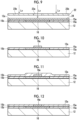
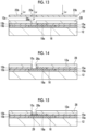
- one example of a suitable aspect of the method for manufacturing a structure is a method for manufacturing a structure, including a step of applying a photosensitive composition containing magnetic particles onto a substrate to form a composition layer; a step of subjecting the composition layer to an exposure treatment and a development treatment to form a first magnetic body portion on the substrate; a step of forming a first insulating layer on the first magnetic body portion; a step of forming a planar inductor having an opening portion on the first insulating layer; a step of applying the photosensitive composition onto the planar inductor to form a composition layer, and subjecting the composition layer to an exposure treatment and a development treatment to form a third magnetic body portion in the opening portion of the planar inductor; a step of forming a second insulating layer on the planar inductor; and a step of applying the photosensitive composition onto the second insulating layer formed on the planar inductor to form a composition layer, and subjecting the composition layer to
- another example of the suitable aspect of the method for manufacturing a structure according to the embodiment of the present invention is a method for manufacturing a structure, including a step of applying a curable composition containing magnetic particles in a patterned manner onto a substrate to form a first patterned composition layer, and subjecting the first patterned composition layer to a curing treatment to form a first magnetic body portion; a step of forming a first insulating layer on the first magnetic body portion; a step of forming a planar inductor having an opening portion on the insulating layer; a step of applying the curable composition in a patterned manner onto the opening portion of the planar inductor to form a third patterned composition layer, and subjecting the third patterned composition layer to a curing treatment to form a third magnetic body portion; a step of forming a second insulating layer on the planar inductor; and a step of applying the curable composition in a patterned manner onto the second insulating layer formed on the planar inductor to form a second
- the curable composition used in the above-mentioned method contains a component that can be cured by a curing treatment.
- the component that can be cured include the above-mentioned polymerizable compound.
- Examples of the method of applying a curable composition in a patterned manner in the above-mentioned method include a screen printing method and an ink jet method.
- the type of the curing treatment is not particularly limited, and examples thereof include a thermal curing treatment and a photo curing treatment.
- the first patterned composition layer of the above-mentioned method is for forming the above-mentioned first magnetic body portion and has, for example, the same shape as the first magnetic body portion.
- the second patterned composition layer is for forming the above-mentioned second magnetic body portion and has, for example, the same shape as the second magnetic body portion.
- the third patterned composition layer is for forming the above-mentioned third magnetic body portion and has, for example, the same shape as the third magnetic body portion.
- the present invention is basically configured as described above. Although the structure and the method for manufacturing a structure according to the embodiment of the present invention have been described in detail above, the present invention is not limited to the above-mentioned embodiments, and various modifications or changes can be made without departing from the spirit and scope of the present invention.
- a configuration in which the planar inductor 14 (see Fig. 1 and Fig. 2 ) was disposed on a substrate was used.
- the size of the substrate was 700 ⁇ m ⁇ 300 ⁇ m.
- the planar inductor 14 was set to have an octagonal outer shape with a maximum outer width of 115 ⁇ m and a maximum inner width of 68 ⁇ m.
- the planar inductor 14 has the opening portion 14b similar in shape to the outer shape of the planar inductor 14, and the opening portion is of an octagon.
- the maximum width of the opening portion was set to 68 ⁇ m.
- the strip-shaped member of the planar inductor 14 was set to have a thickness of 10 ⁇ m and a width of 10 ⁇ m.
- the width of an input portion of the planar inductor 14 was set to 10 ⁇ m.
- the number of turns of the planar inductor 14 was set to 2, and a gap between the turns was set to 5 ⁇ m.
- the magnetic body volume amounts of the first magnetic body portion, the second magnetic body portion, and the third magnetic body portion were obtained to evaluate the amounts of the magnetic bodies used.
- the magnetic body volume amount and the ratio of the area of the third magnetic body were calculated using the volume integral values and area integral values of the computer aided design (CAD) data of the planar inductor, and the first magnetic body portion, the second magnetic body portion, and the third magnetic body portion used in the simulation.
- CAD computer aided design
- the shapes of the planar inductor 14, and the first magnetic body portion, the second magnetic body portion, and the third magnetic body portion were designed using AutoDesk Inventor (registered trademark).
- the designed CAD data was exported to COMSOL Multiphysics (registered trademark), and in order to obtain the resonance frequency, the frequency dependence of the electric field and the magnetic field was calculated by solving the Helmholtz wave equation shown in Expression (a) and Expression (b) using the physical study of electromagnetic waves (frequency range) in COMSOL Multiphysics (registered trademark).
- ⁇ r ⁇ ' - ⁇ " ⁇ j, where ⁇ ' is a real part of a magnetic permeability and ⁇ " is an imaginary part of the magnetic permeability.
- k 0 ⁇ ( ⁇ 0 ⁇ 0 ) 1/2 (m -1 ), where ⁇ is an angular velocity, i is a current, ⁇ 0 is a magnetic permeability in vacuum, and ⁇ 0 is a dielectric constant in vacuum.
- the liquid temperature of the first liquid was set to 25°C and then, while maintaining this liquid temperature, 39.8 g of a sodium hydroxide aqueous solution having a concentration of 1 mol/L was added to obtain a second liquid.
- the pH (hydrogen ion exponent) of the obtained second liquid was 10.5 ⁇ 0.5.
- the pH was measured using a desktop pH meter (F-71, manufactured by Horiba, Ltd.).
- the second liquid was stirred for 15 minutes to obtain a liquid containing a precipitate serving as a precursor of magnetoplumbite type hexagonal ferrite (precursor-containing liquid).
- the precursor-containing liquid was subjected to a centrifugation treatment (rotation speed: 2000 revolutions per minute (rpm), rotation time: 10 minutes) three times, and the resulting precipitate was recovered and washed with water.
- the recovered precipitate was dried in an oven at an internal atmospheric temperature of 95°C for 12 hours to obtain a powder of the precursor.
- the powder of the precursor was placed in a muffle furnace, and the temperature inside the furnace was set to 1100°C in an air atmosphere and the powder was fired for 4 hours to obtain a lumpy sintered product.
- the obtained sintered product was pulverized for 90 seconds using a cutter mill (WONDER CRUSHER WC-3, manufactured by Osaka Chemical Co., Ltd.) as a pulverizer, with a variable speed dial of the pulverizer set to "5" (rotation speed: about 10000 to 15000 rpm), to obtain a magnetic powder (barium ferrite M-1).
- a cutter mill WONDER CRUSHER WC-3, manufactured by Osaka Chemical Co., Ltd.
- a variable speed dial of the pulverizer set to "5" (rotation speed: about 10000 to 15000 rpm)
- the average primary particle diameter of barium ferrite M-1 is 110 nm.
- the crystal structure of the magnetic body constituting the above-mentioned magnetic powder was identified by X-ray diffraction analysis.
- X'Pert Pro manufactured by Malvern Panalytical Ltd.
- the measurement conditions are shown below.
- the obtained magnetic powder was a powder of single-phase magnetoplumbite type hexagonal ferrite having a magnetoplumbite type crystal structure and not containing any crystal structure other than the magnetoplumbite type crystal structure.
- Strontium ferrite M-2 synthesized by the following method.
- the dried mixture was stirred and pulverized for 2 minutes using the Wonder Crush/Mill to obtain a precursor of a magnetic powder.
- the obtained precursor was placed in a muffle furnace, and the temperature inside the furnace was set to a temperature condition of 1250°C in an air atmosphere and the precursor was fired for 4 hours to obtain a sintered product.
- the obtained sintered product was stirred and pulverized for 2 minutes using the Wonder Crush/Mill, repeatedly washed with water, and then dried in a drying device with an internal atmospheric temperature of 95°C.
- the average primary particle diameter of strontium ferrite M-2 is 90 nm.
- X-1 a resin represented by the following structural formula.
- the numerical value in each repeating unit in the following formulae represents the content (% by mass) of each repeating unit with respect to all the repeating units.
- X-2 a resin represented by the following structural formula.
- the numerical value in each repeating unit in the following formulae represents the content (% by mass) of each repeating unit with respect to all the repeating units.
- B-1 a resin represented by the following structural formula.
- the numerical value in each repeating unit in the following formulae represents the content (% by mass) of each repeating unit with respect to all the repeating units.
- the average primary particle diameter of Fe-Mn-based ferrite P-1 is 40 ⁇ m.
- P-2 product name "AW2-08 PF-3F” (Fe-based amorphous alloy particles, manufactured by Epson Atmix Corporation, concentration of solid contents: 100% by mass, volume average particle diameter: 3 ⁇ m)
- composition prepared above was applied onto a substrate to form a composition layer. Then, the composition layer was subjected to a drying treatment at 100°C for 2 minutes.
- the thickness of the composition layer was adjusted by adjusting the application amount of the composition such that the film thickness of the first magnetic body portion was 10 ⁇ m.
- the substrate was a silicon substrate.
- composition layer was subjected to an exposure treatment under the condition of 10 mJ/cm 2 using a simple USHIO exposure device through a photo mask having a predetermined opening portion so that the first magnetic body portion 16 as shown in Fig. 4 was formed.
- a shower development treatment was carried out at 23°C for 60 seconds using a simple development device (manufactured by Mikasa Corporation).
- An aqueous solution having a content of tetramethylammonium hydroxide (TMAH) of 0.3% by mass was used as the developer.
- a rinsing treatment by spin showering using pure water was carried out, followed by spin drying and then a heat treatment (post-baking) for 5 minutes using a hot plate at 220°C to form a first magnetic body portion having a predetermined shape.
- the second magnetic body portion and the third magnetic body portion were formed in positions and shapes according to the configuration of the structure.
- the prepared paste composition was applied onto a substrate so that the first magnetic body portion 16 as shown in Fig. 4 was formed, thereby forming a composition layer.
- the thickness of the composition layer was adjusted by adjusting the application amount of the composition such that the film thickness of the first magnetic body portion was 10 ⁇ m.
- a slit coating method was used as the method of applying the paste composition onto the substrate. After the application of the composition, a drying treatment was carried out as necessary. The drying (pre-baking) was carried out in an oven at a temperature of 50°C to 140°C for 10 to 1800 seconds.
- a structure having a first magnetic body portion, a second magnetic body portion, and a third magnetic body portion was manufactured according to the same procedure as described above, except that the patterns of the first magnetic body portion, the second magnetic body portion, and the third magnetic body portion were made as described later, and the photosensitive compositions or paste compositions for forming the first magnetic body portion, the second magnetic body portion, and the third magnetic body portion were prepared based on the formulations shown in Tables 1 and 2 which will be give later.
- Example 1 was set to have Formulation 1, and the disposition of the first magnetic body portion, the second magnetic body portion, and the third magnetic body portion was set to the disposition shown in Fig. 20 and Fig. 21 .
- Example 2 was set to have Formulation 1, and the disposition of the first magnetic body portion, the second magnetic body portion, and the third magnetic body portion was set to the disposition shown in Fig. 22 .
- Example 3 was set to have Formulation 1, and the disposition of the first magnetic body portion, the second magnetic body portion, and the third magnetic body portion was set to the disposition shown in Fig. 23 .
- Example 5 was set to have Formulation 1, and the disposition of the first magnetic body portion, the second magnetic body portion, and the third magnetic body portion was set to the disposition shown in Fig. 25 .
- Example 6 was set to have Formulation 2, and the disposition of the first magnetic body portion, the second magnetic body portion, and the third magnetic body portion was set to the disposition shown in Fig. 25 .
- Example 7 was set to have Formulation 3, and the disposition of the first magnetic body portion, the second magnetic body portion, and the third magnetic body portion was set to the disposition shown in Fig. 25 .
- Example 8 was set to have Formulation 4, and the disposition of the first magnetic body portion, the second magnetic body portion, and the third magnetic body portion was set to the disposition shown in Fig. 25 .
- Example 9 was set to have Formulation 5, and the disposition of the first magnetic body portion, the second magnetic body portion, and the third magnetic body portion was set to the disposition shown in Fig. 25 .
- Example 10 was set to have Formulation 6, and the disposition of the first magnetic body portion, the second magnetic body portion, and the third magnetic body portion was set to the disposition shown in Fig. 25 .
- Example 12 was set to have Formulation 8, and the disposition of the first magnetic body portion, the second magnetic body portion, and the third magnetic body portion was set to the disposition shown in Fig. 25 .
- Example 13 was set to have Formulation 9, and the disposition of the first magnetic body portion, the second magnetic body portion, and the third magnetic body portion was set to the disposition shown in Fig. 25 .
- Example 14 was set to have Formulation 1, and the disposition of the first magnetic body portion, the second magnetic body portion, and the third magnetic body portion was set to the disposition shown in Fig. 26 .
- Example 16 was set to have Formulation 11, and the disposition of the first magnetic body portion, the second magnetic body portion, and the third magnetic body portion was set to the disposition shown in Fig. 26 .
- Example 19 was set to have Formulation 14, and the disposition of the first magnetic body portion, the second magnetic body portion, and the third magnetic body portion was set to the disposition shown in Fig. 26 .
- Example 20 was set to have Formulation 15, and the disposition of the first magnetic body portion, the second magnetic body portion, and the third magnetic body portion was set to the disposition shown in Fig. 26 .
- Example 21 was set to have Formulation 1, and the first magnetic body portion, the second magnetic body portion, and the third magnetic body portion were configured as shown in Fig. 20 , such that the extending portion of the first magnetic body portion and the extending portion of the second magnetic body portion were not disposed between the two strip-shaped members connected to the power supply port of the planar inductor. That is, Example 21 had a configuration in which the extending portion of the first magnetic body portion and the extending portion of the second magnetic body portion were not disposed between the two strip-shaped members connected to the power supply port of the planar inductor in Example 1.
- Example 21 has a configuration in which the connecting portion 30 is not provided in the structure 10h shown in Fig. 28 .
- Fig. 36 to Fig. 41 the same components as those of the structure 10 shown in Fig. 1 and Fig. 2 are denoted by the same reference numerals, and the detailed description thereof will be omitted.
- the substrate 12, the interlayer insulating layer 15b of the first insulating layer 15, and the second insulating layer 19 shown in Fig. 1 are not shown in Fig. 36 to Fig. 41 .
- the disposition of the third magnetic body portion 102 was set to the disposition shown in Fig. 37 .
- the third magnetic body portion 102 was configured to have a 5-layer structure.
- the third magnetic body portion 102 of Comparative Example 3 is formed by laminating five magnetic bodies 102a.
- the shield insulating layer 15a is disposed between the magnetic bodies 102a, and the magnetic bodies 102a are electrically insulated from each other.
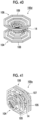
- the first magnetic body portion 104 has a plurality of members 105 having an octagonal outer shape disposed so that centers of the members 105 coincide with each other.
- the second magnetic body portion 106 has a plurality of members 107 having an octagonal outer shape disposed so that centers of the members 107 coincide with each other.
- Comparative Example 9 had a configuration in which the third magnetic body portion was not provided, and the disposition of the first magnetic body portion 104 and the second magnetic body portion 106 was set to the disposition shown in Fig. 39 .
- the first magnetic body portion 104 is composed of a plurality of octagonal members 105 having similar outer shapes but different sizes.
- the plurality of members 105 are disposed to be shifted in an up-down direction with the centers of the members 105 coinciding with each other and the member having a large outer shape facing the planar inductor 14 side.
- the second magnetic body portion 106 is also composed of a plurality of octagonal members 107 having similar outer shapes but different sizes.
- Comparative Example 12 had a configuration in which the third magnetic body portion of Example 21 was not provided.
- Comparative Example 15 had a configuration in which the third magnetic body portion of Example 26 was not provided.
- the magnetic body volume amount is referred to as "MM amount”
- the inductance ratio is referred to as “L/L0”
- the resonance frequency ratio is referred to as “fr/fr0”
- the ratio of the area occupied by the third magnetic body portion is referred to as "Space ratio of third magnetic body portion”.
- Comparative Example 1 had a configuration in which the magnetic body portion was not provided, "None” was written in the columns of "MM amount” and "Space ratio of third magnetic body portion".
Landscapes
- Engineering & Computer Science (AREA)
- Power Engineering (AREA)
- Chemical & Material Sciences (AREA)
- Dispersion Chemistry (AREA)
- Microelectronics & Electronic Packaging (AREA)
- Manufacturing & Machinery (AREA)
- Physics & Mathematics (AREA)
- Spectroscopy & Molecular Physics (AREA)
- Coils Or Transformers For Communication (AREA)
Abstract
Description
- The present invention relates to a structure having a planar inductor and a magnetic body portion, and a method for manufacturing a structure.
- Currently, a mobile communication terminal such as a mobile phone or a smartphone, and an electronic apparatus such as a personal computer use electronic components such as a central processing unit (CPU), a power amplifier, a converter, an active element, and a passive element to realize various types of processing.
- For example, a planar magnetic element is proposed as the passive element in
JP1997-134820A JP-H09-134820A - The planar magnetic element in
JP1997-134820A JP-H09-134820A - For example, a CPU, a power amplifier, and a converter require an electric power source for driving, and a planar inductor is used for removing noise from a voltage supplied by the electric power source. The planar inductor is required to have a high Q value because the performance of noise removal is excellent in a case where the Q value is high. The planar inductor is also referred to as a planar inductor.
- With multifunctionalization and miniaturization of electronic apparatus in recent years, there has also been a demand for miniaturization of electronic components. There has also been a demand for miniaturization of the above-mentioned planar inductor while maintaining the performance such as the Q value.
- The planar magnetic element in
JP1997-134820A JP-H09-134820A - An object of the present invention is to provide a structure having a high Q value and a small size, and a method for manufacturing a structure.
- The above-mentioned object can be achieved by the following configurations.
- Invention [1] is a structure including a substrate and a planar inductor disposed on the substrate, in which the structure further includes a first magnetic body portion disposed on a substrate side with respect to the planar inductor with a first insulating layer interposed therebetween, a second magnetic body portion disposed on a side opposite to the substrate side with respect to the planar inductor with a second insulating layer interposed therebetween, and a third magnetic body portion disposed on a center portion of the planar inductor, at least a part of the first magnetic body portion, the second magnetic body portion, and the third magnetic body portion overlap with each other in a normal direction of the substrate, the first magnetic body portion consists of a first center portion and a plurality of extending portions extending outward from the first center portion in an in-plane direction, or consists of a flat plate portion that covers at least a part of a region from a center of the planar inductor to an outside, and the second magnetic body portion consists of a second center portion and a plurality of extending portions extending outward from the second center portion in the in-plane direction, or consists of a flat plate portion that covers at least a part of a region from the center of the planar inductor to the outside.
- Invention [2] is the structure according to Invention [1], in which a magnetic permeability of each of the first magnetic body portion, the second magnetic body portion, and the third magnetic body portion is 1 to 10000 at a frequency of 10 MHz to 500 MHz, 1 to 1000 at a frequency of more than 500 MHz and 10 GHz or less, and 1 to 100 at a frequency of more than 10 GHz and 100 GHz or less.
- Invention [3] is the structure according to Invention [1] or [2], in which a ratio of an area occupied by the third magnetic body portion to an area of an opening portion provided in the center portion of the planar inductor is 25% or more.
- Invention [4] is the structure according to any one of Inventions [1] to [3], in which the number of the extending portions of the first magnetic body portion and the number of the extending portions of the second magnetic body portion are each 4 or more.
- Invention [5] is the structure according to any one of Inventions [1] to [4], in which at least one of the first magnetic body portion, the second magnetic body portion, or the third magnetic body portion is formed of a composition containing magnetic particles, an alkali-soluble resin, and a polymerizable compound.
- Invention [6] is the structure according to any one of Inventions [1] to [4], in which at least one of the first magnetic body portion, the second magnetic body portion, or the third magnetic body portion contains magnetic particles, and the magnetic particles contain at least one metal element of Ni, Co, or Fe and have an average primary particle diameter of 20 to 1000 nm.
- Invention [7] is the structure according to any one of Inventions [1] to [6], in which a thickness of each of the first magnetic body portion, the second magnetic body portion, and the third magnetic body portion is 300 µm or less.
- Invention [8] is a method for manufacturing the structure according to any one of Inventions [1] to [7], the method including a step of applying a photosensitive composition containing magnetic particles onto a substrate to form a composition layer; a step of subjecting the composition layer to an exposure treatment and a development treatment to form a first magnetic body portion on the substrate; a step of forming a first insulating layer on the first magnetic body portion; a step of forming a planar inductor having an opening portion on the first insulating layer; a step of applying the photosensitive composition onto the planar inductor to form a composition layer, and subjecting the composition layer to an exposure treatment and a development treatment to form a third magnetic body portion in the opening portion of the planar inductor; a step of forming a second insulating layer on the planar inductor; and a step of applying the photosensitive composition onto the second insulating layer formed on the planar inductor to form a composition layer, and subjecting the composition layer to an exposure treatment and a development treatment to form a second magnetic body portion.
- Invention [9] is a method for manufacturing the structure according to any one of Inventions [1] to [7], the method including a step of applying a curable composition containing magnetic particles in a patterned manner onto a substrate to form a first patterned composition layer, and subjecting the first patterned composition layer to a curing treatment to form a first magnetic body portion; a step of forming a first insulating layer on the first magnetic body portion; a step of forming a planar inductor having an opening portion on the insulating layer; a step of applying the curable composition in a patterned manner onto the opening portion of the planar inductor to form a third patterned composition layer, and subjecting the third patterned composition layer to a curing treatment to form a third magnetic body portion; a step of forming a second insulating layer on the planar inductor; and a step of applying the curable composition in a patterned manner onto the second insulating layer formed on the planar inductor to form a second patterned composition layer, and subjecting the second patterned composition layer to a curing treatment to form a second magnetic body portion.
- Invention [10] is the method for manufacturing a structure according to Invention [8] or [9], in which the magnetic particles contain at least one metal element of Ni, Co, or Fe and have an average primary particle diameter of 20 to 1000 nm.
- According to the present invention, it is possible to provide a structure having a high Q value and a small size, and a method for manufacturing the same.
-
-
Fig. 1 is a schematic cross-sectional view showing a first example of a structure according to an embodiment of the present invention. -
Fig. 2 is a schematic perspective view showing an example of a planar inductor used in the first example of the structure according to the embodiment of the present invention. -
Fig. 3 is a schematic view showing an example of a measurement result of the structure according to the embodiment of the present invention. -
Fig. 4 is a schematic cross-sectional view showing an example of a method for manufacturing the first example of the structure according to the embodiment of the present invention. -
Fig. 5 is a schematic cross-sectional view showing an example of a method for manufacturing the first example of the structure according to the embodiment of the present invention. -
Fig. 6 is a schematic cross-sectional view showing an example of a method for manufacturing the first example of the structure according to the embodiment of the present invention. -
Fig. 7 is a schematic cross-sectional view showing an example of a method for manufacturing the first example of the structure according to the embodiment of the present invention. -
Fig. 8 is a schematic cross-sectional view showing an example of a method for manufacturing the first example of the structure according to the embodiment of the present invention. -
Fig. 9 is a schematic cross-sectional view showing an example of a method for manufacturing the first example of the structure according to the embodiment of the present invention. -
Fig. 10 is a schematic cross-sectional view showing an example of a method for manufacturing the first example of the structure according to the embodiment of the present invention. -
Fig. 11 is a schematic cross-sectional view showing an example of a method for manufacturing the first example of the structure according to the embodiment of the present invention. -
Fig. 12 is a schematic cross-sectional view showing an example of a method for manufacturing the first example of the structure according to the embodiment of the present invention. -
Fig. 13 is a schematic cross-sectional view showing an example of a method for manufacturing the first example of the structure according to the embodiment of the present invention. -
Fig. 14 is a schematic cross-sectional view showing an example of a method for manufacturing the first example of the structure according to the embodiment of the present invention. -
Fig. 15 is a schematic cross-sectional view showing an example of a method for manufacturing the first example of the structure according to the embodiment of the present invention. -
Fig. 16 is a schematic cross-sectional view showing an example of a method for manufacturing the first example of the structure according to the embodiment of the present invention. -
Fig. 17 is a schematic cross-sectional view showing an example of a method for manufacturing the first example of the structure according to the embodiment of the present invention. -
Fig. 18 is a schematic cross-sectional view showing an example of a method for manufacturing the first example of the structure according to the embodiment of the present invention. -
Fig. 19 is a schematic cross-sectional view showing an example of a method for manufacturing the first example of the structure according to the embodiment of the present invention. -
Fig. 20 is a schematic perspective view showing a second example of the structure according to the embodiment of the present invention. -
Fig. 21 is a schematic side view showing the second example of the structure according to the embodiment of the present invention. -
Fig. 22 is a schematic perspective view showing a third example of the structure according to the embodiment of the present invention. -
Fig. 23 is a schematic perspective view showing a fourth example of the structure according to the embodiment of the present invention. -
Fig. 24 is a schematic perspective view showing a fifth example of the structure according to the embodiment of the present invention. -
Fig. 25 is a schematic perspective view showing a sixth example of the structure according to the embodiment of the present invention. -
Fig. 26 is a schematic perspective view showing a seventh example of the structure according to the embodiment of the present invention. -
Fig. 27 is a schematic perspective view showing an eighth example of the structure according to the embodiment of the present invention. -
Fig. 28 is a schematic perspective view showing a ninth example of the structure according to the embodiment of the present invention. -
Fig. 29 is a schematic perspective view showing a tenth example of the structure according to the embodiment of the present invention. -
Fig. 30 is a schematic perspective view showing an eleventh example of the structure according to the embodiment of the present invention. -
Fig. 31 is a schematic perspective view showing a twelfth example of the structure according to the embodiment of the present invention. -
Fig. 32 is a schematic perspective view showing a thirteenth example of the structure according to the embodiment of the present invention. -
Fig. 33 is a schematic perspective view showing a fourteenth example of the structure according to the embodiment of the present invention. -
Fig. 34 is a schematic perspective view showing a fifteenth example of the structure according to the embodiment of the present invention. -
Fig. 35 is a schematic perspective view showing a sixteenth example of the structure according to the embodiment of the present invention. -
Fig. 36 is a schematic perspective view showing a structure of Comparative Example 2. -
Fig. 37 is a schematic perspective view showing a structure of Comparative Example 3. -
Fig. 38 is a schematic perspective view showing a structure of Comparative Example 8. -
Fig. 39 is a schematic perspective view showing a structure of Comparative Example 9. -
Fig. 40 is a schematic perspective view showing a structure of Comparative Example 10. -
Fig. 41 is a schematic perspective view showing a structure of Comparative Example 11. - Hereinafter, a structure and a method for manufacturing a structure according to the embodiment of the present invention will be described in detail with reference to suitable embodiments shown in the accompanying drawings.
- It should be noted that the drawings described below are only illustrative for explaining the present invention, and the present invention is not limited to the drawings shown below.
- In addition, the drawings described below are drawings in which a portion of a planar inductor and portions of a first magnetic body portion, a second magnetic body portion, and a third magnetic body portion in an actual device are emphasized, and illustrations of an electric circuit, a copper wire, a waveguide, and the like around the planar inductor are omitted.
- In the following, the expression "to" indicating a numerical range includes numerical values written on both sides of "to". For example, in a case where ε is a value between a numerical value εα and a numerical value εβ, the range of ε is a range including the numerical value εα and the numerical value εβ and is expressed by εα ≤ ε ≤ εβ in mathematical symbols.
- Unless otherwise specified, angles include an error range generally acceptable in the relevant technical field.
-
Fig. 1 is a schematic cross-sectional view showing a first example of the structure according to the embodiment of the present invention, andFig. 2 is a schematic perspective view showing an example of a planar inductor used in the first example of the structure according to the embodiment of the present invention. - As shown in
Fig. 1 , astructure 10 includes asubstrate 12 and aplanar inductor 14 disposed on thesubstrate 12. - In the
structure 10, a firstmagnetic body portion 16 is disposed on thesubstrate 12 side with respect to theplanar inductor 14 with a first insulatinglayer 15 interposed therebetween. The first insulatinglayer 15 provided on asurface 12a of thesubstrate 12 is an electrical insulating film. The first insulatinglayer 15 includes, for example, ashield insulating layer 15a and an interlayer insulatinglayer 15b. The first insulatinglayer 15 is configured such that theshield insulating layer 15a and the interlayer insulatinglayer 15b are laminated in this order from thesubstrate 12 side. In the first insulatinglayer 15, the number of laminated layers of theshield insulating layers 15a and theinterlayer insulating layers 15b is four layers inFig. 1 , but is not particularly limited. - The first
magnetic body portion 16 is disposed between theshield insulating layer 15a provided on thesurface 12a of thesubstrate 12 and theshield insulating layer 15a disposed on theinterlayer insulating layer 15b on thesubstrate 12 side. The firstmagnetic body portion 16 is embedded in theinterlayer insulating layer 15b. - The
shield insulating layer 15a provides electrical insulation while suppressing diffusion of the material constituting theplanar inductor 14 and the materials constituting the firstmagnetic body portion 16, a secondmagnetic body portion 17, and a thirdmagnetic body portion 18. The interlayer insulatinglayer 15b is thicker than theshield insulating layer 15a and provides electrical insulation over a large range. - The second
magnetic body portion 17 is disposed on a side opposite to thesubstrate 12 side with respect to theplanar inductor 14 with a second insulatinglayer 19 interposed therebetween. The second insulatinglayer 19 is an electrical insulating film, and includes ashield insulating layer 15a and an interlayer insulatinglayer 15b, similarly to the first insulatinglayer 15. Theshield insulating layer 15a is provided between theplanar inductor 14 and the secondmagnetic body portion 17. The secondmagnetic body portion 17 is embedded in theinterlayer insulating layer 15b of the second insulatinglayer 19. - The first
magnetic body portion 16 and the thirdmagnetic body portion 18 are electrically insulated from theplanar inductor 14 by the first insulatinglayer 15. In addition, the firstmagnetic body portion 16 and the thirdmagnetic body portion 18 are electrically insulated from each other by the first insulatinglayer 15, that is, the laminatedshield insulating layer 15a and interlayer insulatinglayer 15b. The secondmagnetic body portion 17 and theplanar inductor 14 are electrically insulated from each other by the second insulatinglayer 19. - The third
magnetic body portion 18 shown inFig. 1 is composed of, for example, threemagnetic bodies magnetic bodies magnetic bodies magnetic body 18c is disposed in anopening portion 14b (seeFig. 2 ) of theplanar inductor 14. All of the threemagnetic bodies shield insulating layers 15a and embedded in theinterlayer insulating layers 15b. As a result, the threemagnetic bodies - In
Fig. 1 , the thirdmagnetic body portion 18 is composed of threemagnetic bodies magnetic body portion 18 is not particularly limited. - The first
magnetic body portion 16, the secondmagnetic body portion 17, and the thirdmagnetic body portion 18 are collectively referred to simply as amagnetic body portion 20. - The
planar inductor 14 is a passive element. Theplanar inductor 14 is, for example, a coil as shown inFig. 2 and is composed of, for example, a strip-shapedmember 14a having a predetermined number of turns. - The
planar inductor 14 has, for example, a circular outer shape or a polygonal outer shape such as an octagon. Theplanar inductor 14 has theopening portion 14b that is open with respect to thesurface 12a of thesubstrate 12. Theopening portion 14b of theplanar inductor 14 is a region surrounded by the strip-shapedmember 14a. - The strip-shaped
member 14a of theplanar inductor 14 is provided with apower supply port 14c. The two strip-shapedmembers 14a are electrically connected to thepower supply port 14c. A voltage is applied to theplanar inductor 14 through thepower supply port 14c. - The coil shown by the
planar inductor 14 can be used alone as an inductor. Theplanar inductor 14 is used, for example, to remove noise of a voltage. For example, a voltage after removing noise by passing a voltage through theplanar inductor 14 is supplied to the CPU. This makes it possible to suppress the malfunction of the CPU. - The
planar inductor 14 is disposed on thesubstrate 12 together with themagnetic body portion 20 described above. - The
planar inductor 14 is composed of, for example, copper. Theplanar inductor 14 has, for example, an outer diameter of 5 to 1000 µm, a width of the strip-shapedmember 14a of 0.5 to 500 µm, a thickness of the strip-shapedmember 14a of 0.05 to 100 µm, and the number of turns of the strip-shapedmember 14a of 1 to 10. - Preferably, the
planar inductor 14 has an outer diameter of 10 to 300 µm, a width of the strip-shapedmember 14a of 2 to 100 µm, a thickness of the strip-shapedmember 14a of 0.5 to 50 µm, and the number of turns of the strip-shapedmember 14a of 1 to 5. - In the
structure 10, at least a part of the firstmagnetic body portion 16, the secondmagnetic body portion 17, and the thirdmagnetic body portion 18 overlap with each other in a normal direction of thesubstrate 12. - The first
magnetic body portion 16 and the secondmagnetic body portion 17 each consist of a flat plate portion that covers at least a part of a region from the center of theplanar inductor 14 to the outside. The center of theplanar inductor 14 is a geometric center of theopening portion 14b. In addition, for example, the firstmagnetic body portion 16 and the secondmagnetic body portion 17 have a congruent shape relationship. - In addition, the positions of the first
magnetic body portion 16 and the secondmagnetic body portion 17 relative to the thirdmagnetic body portion 18 are also the same in the normal direction of thesubstrate 12 of thestructure 10, that is, in a case of being viewed from a direction perpendicular to thesurface 12a of thesubstrate 12. In this case, the outer shape of the firstmagnetic body portion 16 and the outer shape of the secondmagnetic body portion 17 overlap with each other upon being viewed from a direction perpendicular to thesurface 12a of thesubstrate 12. This is preferable because a large number of magnetic lines generated at theopening portion 14b of theplanar inductor 14 pass through the firstmagnetic body portion 16 and the secondmagnetic body portion 17, so leakage magnetism is further suppressed. - The
substrate 12 is composed of, for example, Si, polyimide, or SiO2. - The
shield insulating layer 15a and the interlayer insulatinglayer 15b constituting the first insulatinglayer 15 and the second insulatinglayer 19 are not particularly limited as long as theshield insulating layer 15a and the interlayer insulatinglayer 15b have electrical insulating properties, and are composed of, for example, SiN, TiN, SiO2, tetraethoxysilane (TEOS), and borophosphosilicate glass (BPSG). In addition, thesubstrate 12, the first insulatinglayer 15, and the second insulatinglayer 19 can also be composed of a glass epoxy resin such as flame retardant (FR)-4, polytetrafluoroethylene (PTFE), or the like. - The
shield insulating layer 15a and the interlayer insulatinglayer 15b constituting the first insulatinglayer 15 and the second insulatinglayer 19 are different from themagnetic body portion 20. It is preferable that the magnetic permeability of theshield insulating layer 15a and the interlayer insulatinglayer 15b constituting the first insulatinglayer 15 and the second insulatinglayer 19 does not satisfy the following requirements 1 to 3. - Requirement 1: the magnetic permeability at a frequency of 10 MHz to 500 MHz is 1 to 10000
- Requirement 2: the magnetic permeability at a frequency of more than 500 MHz and 10 GHz or less is 1 to 1000
- Requirement 3: the magnetic permeability at a frequency of more than 10 GHz and 100 GHz or less is 1 to 100
- The
structure 10 is used, for example, in an antenna-in-package, and is provided with, for example, an array antenna, an A/D circuit, a memory, and an application specific integrated circuit (ASIC), which are not shown, in addition to the above-mentionedplanar inductor 14. The A/D circuit, memory, and ASIC are composed of, for example, various semiconductor elements. - In addition, the
structure 10 has, in addition to the above-mentioned configuration, various circuits, elements, and the like that a mobile communication terminal such as a smartphone or a wireless communication module has, for example, a radio frequency (RF) circuit, a power amplifier for transmission, a low noise amplifier for reception, an integrated passive element, a switch, and a phase shifter. - The
substrate 12 functions as a support for thestructure 10, and the above-mentionedplanar inductor 14 is disposed thereon. In addition, themagnetic body portion 20 is disposed on thesubstrate 12. In addition, the A/D circuit, memory, ASIC, and the like constituting the above-mentioned antenna-in-package may be disposed on thesubstrate 12. - The first insulating
layer 15 and the second insulatinglayer 19 are on which theplanar inductor 14 and themagnetic body portion 20 are formed, and keep theplanar inductor 14 and themagnetic body portion 20 in an electrically insulated state. - The first insulating
layer 15 and the second insulatinglayer 19 are not particularly limited as long as the first insulatinglayer 15 and the second insulatinglayer 19 can electrically insulate theplanar inductor 14 and themagnetic body portion 20, and various layers used in the formation of a semiconductor element or the like can be used. - The first
magnetic body portion 16, the secondmagnetic body portion 17, and the thirdmagnetic body portion 18 increase the inductance of theplanar inductor 14, thereby increasing the Q value and reducing the size. - A large number of magnetic lines generated at the
opening portion 14b of theplanar inductor 14 pass through the firstmagnetic body portion 16 and the secondmagnetic body portion 17, thereby suppressing the leakage magnetic flux and increasing the inductance of theplanar inductor 14. For this reason, it is preferable that the firstmagnetic body portion 16 and the secondmagnetic body portion 17 are configured such that a large number of magnetic lines pass through or are disposed such that a large number of magnetic lines pass through. - The leakage magnetic flux is suppressed, so the effect of magnetic force on other electronic components can be suppressed. As a result, the normal operation of electronic components is also suppressed from being hindered.
- The third
magnetic body portion 18 increases the inductance of theplanar inductor 14 and increases the Q value. As a result, theplanar inductor 14 can be made smaller. - Generally, the
planar inductor 14 has a high inductance in a case where a magnetic body is present. In a case where the size ratio between the coil (the region surrounded by the strip-shapedmember 14a) and the magnetic body is kept constant and the coil (the region surrounded by the strip-shapedmember 14a) is reduced in size, the inductance decreases and eventually reaches the same inductance value as in a case where there is no magnetic body. Therefore, it is possible to calculate the change in size of the coil (the region surrounded by the strip-shapedmember 14a) through simulation to thereby calculate the approximate reducible rate of the designed inductor. - In addition, similarly, the resonance frequency of the
planar inductor 14 also decreases in a case where there is a magnetic body. In a case where the sizes of the coil (the region surrounded by the strip-shapedmember 14a) and the magnetic body are kept constant and the coil (the region surrounded by the strip-shapedmember 14a) is reduced in size, the resonance frequency shifts to a higher frequency side and eventually reaches the same resonance frequency as in a case where there is no magnetic body. Therefore, it is possible to calculate the change in size of the coil (the region surrounded by the strip-shapedmember 14a) through simulation to thereby calculate the approximate reduction rate of the designed inductor. - In the
planar inductor 14, the arrangement of the magnetic body that can reduce the size of the inductor allows the coil (the region surrounded by the strip-shapedmember 14a) to be reduced to a size of approximately 70% to 50%, so it is preferable that the inductance ratio described later is 1.1 or more and the resonance frequency ratio described later is 0.75 or less, and it is more preferable that the inductance ratio described later is more than 1.5 and the resonance frequency ratio described later is less than 0.65. - Here, with regard to the resonance frequency, the change in electromagnetic field of the
planar inductor 14 in a case where a voltage of 1 V is applied to apower supply port 14c of theplanar inductor 14 and the frequency is changed from 100 MHz to 1000 GHz is calculated. The generated magnetic lines are deformed along a magnetic body in a case where the magnetic body is present. - From the obtained graph of the resonance frequency shown in
Fig. 3 , the inclination of the slope in the low frequency region is taken as inductance L (H), and the maximum value of the peak of the impedance is taken as R (Ω). The frequency at the peak of the impedance is taken as the resonance frequency fr (Hz). The capacitance C (F) is calculated from these numerical values according to the following expression. The Q value is calculated according to the following expression using R, L, and C.

- By measuring the value L0 of the inductance in a state where there is no magnetic body portion and the resonance frequency fr0 in a state where there is no magnetic body portion, the changes in inductance and resonance frequency due to the magnetic body portion can be found.
- As the inductance ratio represented by L/L0 is larger and the resonance frequency ratio represented by fr/fr0 is smaller, the size of the
opening portion 14b of theplanar inductor 14 can be reduced. - L is a value of inductance in a state where there is a magnetic body portion. fr is a resonance frequency in a state where there is a magnetic body portion.
- For example, it is preferable that at least one of the first
magnetic body portion 16, the secondmagnetic body portion 17, or the third magnetic body portion 18 (for example, threemagnetic bodies - In addition, for example, it is preferable that at least one of the first
magnetic body portion 16, the secondmagnetic body portion 17, or the third magnetic body portion 18 (for example, threemagnetic bodies - It is preferable that the magnetic permeability of each of the first
magnetic body portion 16, the secondmagnetic body portion 17, and the third magnetic body portion 18 (for example, threemagnetic bodies - In a case where the magnetic permeability of each of the first
magnetic body portion 16, the secondmagnetic body portion 17, and the third magnetic body portion 18 (for example, threemagnetic bodies planar inductor 14 can be increased and the size of theplanar inductor 14 can be reduced as described above. - The magnetic permeability of each of the first magnetic body portion, the second magnetic body portion, and the third magnetic body portion (for example, three
magnetic bodies shield insulating layer 15a and the interlayer insulatinglayer 15b constituting the first insulatinglayer 15 and the second insulatinglayer 19 can also be measured in the same manner as the magnetic permeability of each of the firstmagnetic body portion 16, the secondmagnetic body portion 17, and the thirdmagnetic body portion 18 as described above. - The insulator does not have the performance of the magnetic body, so the result is a value of 1 even in a case of calculation. From this, the magnetic permeability of each of the
shield insulating layer 15a and the interlayer insulatinglayer 15b constituting the first insulatinglayer 15 and the second insulatinglayer 19 is calculated to be 1. - The magnetic permeability is a rate of change of a magnetic flux density (B) that occurs in a case where a magnetic field (H) is applied to a certain material, and is expressed by the following expression.

- In a case of a magnetic body, a larger amount of magnetic flux is passed through the inside of the magnetic body, but a material that is not a magnetic body exhibits no change in magnetic flux, so the value of magnetic permeability is 1. The complex relative magnetic permeability µ is expressed by the following expression. Here, j in the following expression represents an imaginary number. The real part µ' of the complex relative magnetic permeability µ is the magnetic permeability of the present invention.

- In a case where the direction of the current is reversed at a high-frequency wave such as an electromagnetic wave, the real part means the performance as a magnetic body that produces a higher magnetic flux density, whereas µ" of the imaginary part represents an energy loss. Specifically, the magnetic moment of the crystals in the magnetic body tends to orient in the direction of the magnetic field generated by a high-frequency wave, but in a case where the magnetic moment is reversed in an opposite direction, a delay in the reversal time or an energy loss (as heat) occurs.
- In addition, the thickness of each of the first
magnetic body portion 16, the secondmagnetic body portion 17, and the thirdmagnetic body portion 18 is preferably 300 µm or less. In a case where the thickness of each of the firstmagnetic body portion 16, the secondmagnetic body portion 17, and the thirdmagnetic body portion 18 is 300 µm or less, the Q value can be increased and the height of the structure can be reduced. - The thickness of each of the first
magnetic body portion 16, the secondmagnetic body portion 17, and the thirdmagnetic body portion 18 is more preferably 10 to 200 µm, and the lower limit value of the thickness is 5 µm. - The thickness of the third
magnetic body portion 18 refers to a thickness of each of the threemagnetic bodies magnetic body portion 18. - The ratio of an area occupied by the third
magnetic body portion 18 to an area of theopening portion 14b provided in the center portion of theplanar inductor 14 is preferably 25% or more, more preferably 50% or more, and still more preferably 60% or more. The upper limit value of the ratio of the area occupied by the thirdmagnetic body portion 18 is 99.9%. - The ratio (%) of the area occupied by the third
magnetic body portion 18 refers to a percentage of the area of theopening portion 14b filled with the thirdmagnetic body portion 18 with respect to the area of theopening portion 14b of theplanar inductor 14, with the area of theopening portion 14b of theplanar inductor 14 being 100%. That is, it is the area of themagnetic body 18c disposed in theopening portion 14b. - For example, the area of the
opening portion 14b of theplanar inductor 14 and the area of the thirdmagnetic body portion 18 in theopening portion 14b may be actual measured values or may be values obtained from computer aided design (CAD) data used for design. - The antenna-in-package has a configuration in which an antenna and a front end module (FEM) are laminated. The FEM is an arithmetic circuit portion of a wireless circuit that includes a complementary metal oxide semiconductor (CMOS) transistor that controls transmission and reception on the antenna side.
- The array antenna constituting the antenna-in-package has, for example, four antennas. For example, the four antennas are all the same. The configurations of the array antenna and the antenna are not particularly limited and are appropriately determined depending on the frequency band to be transmitted or received, the direction of polarization to be received, and the like. In addition, the array antenna has four antennas, but the configuration of the array antenna is not limited thereto. Instead of an array antenna, a single antenna may be used.
- The A/D circuit converts an analog signal into a digital signal, and a known A-D converter is used. The A/D circuit converts the received signal received by the array antenna through radio waves into a digital signal.
- The ASIC obtains the original data or signal transmitted to the array antenna from the received signal converted into a digital signal. In addition, the ASIC generates transmission data or a transmission signal in a state of a digital signal. The functions of the ASIC are not particularly limited and are appropriately determined depending on the intended use and the like.
- In addition, the A/D circuit converts the transmission data or the transmission signal generated by the ASIC into an analog signal that can be transmitted by the array antenna.
- The memory stores the transmission data or the transmission signal generated in the ASIC, the received signal converted into a digital signal received by the array antenna, and the like. The memory used may be, for example, a volatile memory such as a dynamic random access memory (DRAM), and is preferably a high bandwidth memory (HBM).
- The method for manufacturing the above-mentioned
structure 10 shown inFig. 1 will be described. - Here,
Fig. 4 to Fig. 19 are schematic cross-sectional views showing an example of the method for manufacturing the first example of the structure according to the embodiment of the present invention in the order of steps. InFig. 4 to Fig. 19 , the same components as those of thestructure 10 shown inFig. 1 are denoted by the same reference numerals, and the detailed description thereof will be omitted. - For example, as shown in
Fig. 4 , theshield insulating layer 15a having a thickness of 50 nm to 300 nm is formed on theentire surface 12a of thesubstrate 12 by, for example, physical vapor deposition (PVD) or chemical vapor deposition (CVD). Theshield insulating layer 15a is composed of, for example, SiN or TiN. - Next, a photosensitive composition containing magnetic particles is applied onto the entire surface of the
shield insulating layer 15a to form acomposition layer 21. For example, thecomposition layer 21 is of a negative type, and a non-exposed portion is removed by a development treatment. The thickness of thecomposition layer 21 is not particularly limited, and may be a thickness such that the thickness is 300 µm or less in a case of being formed into the firstmagnetic body portion 16 as described later. - Next, a
photo mask 22 is disposed on thecomposition layer 21 as shown inFig. 4 . In thephoto mask 22, for example, amask portion 23b is provided in a region other than the region where the firstmagnetic body portion 16 is formed. Aregion 23a other than themask portion 23b transmits the exposure light Lv that exposes thecomposition layer 21. Themask portion 23b blocks the exposure light Lv. - The
composition layer 21 exposed to light using thephoto mask 22 is of a negative type as described above, and a non-exposed portion is removed by a development treatment. That is, an exposed portion of thecomposition layer 21 is the firstmagnetic body portion 16. - In a case where the
composition layer 21 is of a positive type, an exposed portion is removed by a development treatment, so that the light shielding region of thephoto mask 22 is opposite to that of thephoto mask 22 shown inFig. 4 . - The method of the development treatment is not particularly limited, and a known development treatment can be applied. Examples of the developer used in the development treatment include an alkali developer and a developer containing an organic solvent.
- The
planar inductor 14 is formed, for example, by a device nanofabrication technique in which steps such as lamination sputtering, physical vapor deposition (PVD), chemical vapor deposition (CVD), photolithography, dry etching, wet etching, plasma ashing, copper electrolytic plating, chemical mechanical polishing (CMP) slurry polishing, and wet etching are combined a plurality of times. - In addition, the
planar inductor 14 can also be formed using an insulating magnetic film. - A photosensitive magnetic body is applied onto the first insulating
layer 15 to form a composition layer. - Next, the composition layer is subjected to exposure through a photo mask having a predetermined opening portion and then a development treatment to form a magnetic pattern having a predetermined shape.
- Next, for example, a Ni film and a Cu film are formed as plating seed layers on the magnetic pattern by vapor deposition. Then, a photoresist film is formed in a patterned manner on the plating seed layer except for the portion where the planar inductance is formed, and then plating is grown in the opening portion of the resist by an electrolytic plating method. Thereafter, the photoresist film is peeled off, and the plating seed layer in the region covered by the photoresist film is removed by a wet etching method. After formation of a SiO2 layer on the magnetic pattern, a Cu layer on the second stage is formed by a photolithography method, and then a photosensitive magnetic body is formed on the inside of the coil by a photolithography method. These steps are repeated to form Cu layers and magnetic body layers, thereby forming the
planar inductor 14. - The
photo mask 22 is disposed on thecomposition layer 21 which is then subjected to exposure and a development treatment to form the firstmagnetic body portion 16 as shown inFig. 5 . - Next, as shown in
Fig. 6 , theinterlayer insulating layer 15b covering the firstmagnetic body portion 16 is formed on theentire surface 12a of thesubstrate 12. - The interlayer insulating
layer 15b is formed by, for example, physical vapor deposition (PVD) or chemical vapor deposition (CVD). As described above, theinterlayer insulating layer 15b is composed of, for example, TEOS or BPSG. - Next, as shown in
Fig. 7 , theinterlayer insulating layer 15b is flattened by an etch-back or chemical mechanical polishing (CMP) process. - After flattening of the interlayer insulating
layer 15b, theshield insulating layer 15a is formed on the entire surface of the interlayer insulatinglayer 15b as shown inFig. 8 . The method for forming theshield insulating layer 15a is as described above. - Next, a
composition layer 24 is formed on the entire surface of theshield insulating layer 15a as shown inFig. 9 . The method for forming thecomposition layer 24 is the same as the method for forming thecomposition layer 21. - The
photo mask 22 is disposed on thecomposition layer 24. In thephoto mask 22, themask portion 23b is provided in a region other than the region where themagnetic body 18a of the thirdmagnetic body portion 18 is formed. Theregion 23a of thephoto mask 22 transmits the exposure light Lv that exposes thecomposition layer 24, and themask portion 23b blocks the exposure light Lv. The exposed portion of thecomposition layer 24 is themagnetic body 18a (seeFig. 10 ). In this manner, themagnetic body 18a is formed by the photolithography method. - After formation of the
magnetic body 18a shown inFig. 10 , theinterlayer insulating layer 15b that covers themagnetic body 18a is formed on theshield insulating layer 15a as shown inFig. 11 . The method for forming the interlayer insulatinglayer 15b is as described above. - Next, as shown in
Fig. 12 , a flattening treatment is carried out on theinterlayer insulating layer 15b. For example, etch-back or CMP is used for the flattening treatment. - Next, a resist film 28 (see
Fig. 13 ) is formed on theinterlayer insulating layer 15b, and thephoto mask 22 is disposed on the resistfilm 28 as shown inFig. 13 . Theregion 23a of thephoto mask 22 transmits the exposure light Lv that exposes the resistfilm 28. The resistfilm 28 is subjected to pattern exposure using thephoto mask 22 and is then developed to form anopening portion 28a in the resistfilm 28. The resistfilm 28 inFig. 14 is of a positive type, and the exposed portion is removed by a development treatment. That is, the exposed portion is theopening portion 28a. A known photolithography method is used for the formation of the resistfilm 28 and the formation of theopening portion 28a of the resistfilm 28. - Next, the
interlayer insulating layer 15b provided with the resistfilm 28 as shown inFig. 13 is etched to form anopening portion 15c in theinterlayer insulating layer 15b reaching the underlyingshield insulating layer 15a as shown inFig. 14 . In this case, theshield insulating layer 15a under theinterlayer insulating layer 15b is not etched. The etching of the interlayer insulatinglayer 15b is not particularly limited and may be wet etching or dry etching. - Next, as shown in
Fig. 15 , ametal layer 29 constituting theplanar inductor 14 is formed in theopening portion 15c by, for example, electrolytic plating. - Next, the resist
film 28 shown inFig. 15 is peeled off. The method for peeling off the resistfilm 28 is not particularly limited. Examples of the method for peeling off the resistfilm 28 include peeling off the resistfilm 28 by ashing and peeling off the resistfilm 28 using a chemical liquid. - After the resist
film 28 is peeled off, theinterlayer insulating layer 15b on which themetal layer 29 is formed is subjected to a flattening treatment. For example, etch-back or CMP is used for the flattening treatment. - Next, after the flattening treatment, the
shield insulating layer 15a shown inFig. 17 is formed on the entire surface of the interlayer insulatinglayer 15b on which themetal layer 29 is formed. The method for forming theshield insulating layer 15a is as described above. - The same steps as those shown in
Fig. 9 to Fig. 16 described above are repeatedly carried out. As a result, as shown inFig. 18 , for example, themagnetic bodies planar inductor 14 can be formed in the first insulatinglayer 15 that is composed of fourshield insulating layers 15a and four interlayer insulatinglayers 15b. Theplanar inductor 14 is formed by laminating themetal layer 29 and the like, and has a configuration in which theshield insulating layer 15a and the interlayer insulatinglayer 15b are not disposed between the metal layers 29. Therefore, theplanar inductor 14 has a configuration with no electrically insulated portion. - Next, as shown in
Fig. 18 , after formation of themagnetic bodies planar inductor 14 in the first insulatinglayer 15, theshield insulating layer 15a (not shown) is formed on theplanar inductor 14 and on the entire surface of the interlayer insulatinglayer 15b around theplanar inductor 14. The method for forming theshield insulating layer 15a is as described above. - Next, as shown in
Fig. 19 , a photosensitive composition is applied onto the entire surface of theshield insulating layer 15a to form acomposition layer 25. Then, aphoto mask 26 is disposed on thecomposition layer 25 which is then subjected to exposure and a development treatment to form the secondmagnetic body portion 17 on theshield insulating layer 15a as shown inFig. 1 . The method for forming thecomposition layer 25 is the same as the method for forming thecomposition layer 21. - In addition, in the
photo mask 26, for example, amask portion 27b is provided in a region other than the region where the secondmagnetic body portion 17 is formed. Aregion 27a other than themask portion 27b transmits the exposure light Lv that exposes thecomposition layer 25. Themask portion 27b blocks the exposure light Lv. The exposed portion of thecomposition layer 25 is the second magnetic body portion 17 (seeFig. 1 ). - The above-mentioned
composition layer 21,composition layer 24, andcomposition layer 25 are formed of, for example, the same photosensitive composition. - After formation of the second magnetic body portion 17 (see
Fig. 1 ) on theshield insulating layer 15a, theinterlayer insulating layer 15b (seeFig. 1 ) is formed on the entire surface of theshield insulating layer 15a to cover the secondmagnetic body portion 17. This results in the formation of thestructure 10 shown inFig. 1 . The method for forming the interlayer insulatinglayer 15b is as described above. -
Fig. 20 is a schematic perspective view showing a second example of the structure according to the embodiment of the present invention andFig. 21 is a schematic side view showing the second example of the structure according to the embodiment of the present invention. InFig. 20 and Fig. 21 , the same components as those of thestructure 10 shown inFig. 1 and theplanar inductor 14 shown inFig. 2 are denoted by the same reference numerals, and the detailed description thereof will be omitted. In addition, inFig. 20 and Fig. 21 , thesubstrate 12, a part of theshield insulating layers 15a and theinterlayer insulating layers 15b constituting the first insulatinglayer 15, and the second insulatinglayer 19 shown inFig. 1 are not shown.Fig. 21 is a side view seen from the same direction as inFig. 1 . - A
structure 10a shown inFig. 20 and Fig. 21 is different from thestructure 10 shown inFig. 1 and theplanar inductor 14 shown inFig. 2 in the configuration of the firstmagnetic body portion 16, the secondmagnetic body portion 17, and the third magnetic body portion 18 (threemagnetic bodies - The
structure 10a has a configuration in which the firstmagnetic body portion 16 consists of afirst center portion 16a and a plurality of extendingportions 16b that extend outward from thefirst center portion 16a in an in-plane direction. Thefirst center portion 16a has a circular outer shape. The number of extendingportions 16b is 4, and the extendingportions 16b are disposed at intervals of 90° with respect to a center Cd of thefirst center portion 16a. That is, the four extendingportions 16b are disposed at equal intervals with respect to the center Cd of thefirst center portion 16a. One of the four extendingportions 16b is disposed between the two strip-shapedmembers 14a connected to thepower supply port 14c of theplanar inductor 14. - The second
magnetic body portion 17 has a similar configuration to the firstmagnetic body portion 16. The secondmagnetic body portion 17 has a configuration which consists of asecond center portion 17a and a plurality of extendingportions 17b that extend outward from thesecond center portion 17a in an in-plane direction. Thesecond center portion 17a has a circular outer shape. The number of extendingportions 17b is 4, and the extendingportions 17b are disposed at intervals of 90° with respect to a center Cd of thesecond center portion 17a. That is, the four extendingportions 17b are disposed at equal intervals with respect to the center Cd of thesecond center portion 17a. One of the four extendingportions 17b is disposed between the two strip-shapedmembers 14a connected to thepower supply port 14c of theplanar inductor 14. - The first
magnetic body portion 16 and the secondmagnetic body portion 17 have the same shape, and in a normal direction of the substrate 12 (seeFig. 1 ) of thestructure 10a, that is, in a case of being viewed from a direction perpendicular to the center Cd of thesecond center portion 17a, the outer shape of the firstmagnetic body portion 16 and the outer shape of the secondmagnetic body portion 17 are disposed to overlap with each other. This is preferable because a large number of magnetic lines generated at theopening portion 14b of theplanar inductor 14 pass through the firstmagnetic body portion 16 and the secondmagnetic body portion 17, so leakage magnetism is further suppressed. - The third
magnetic body portion 18 is not of a single member, but is divided into a plurality of portions, is composed of a plurality of magnetic materials, and is divided into, for example, threemagnetic bodies magnetic bodies shield insulating layer 15a. The number of divisions of the thirdmagnetic body portion 18 is not particularly limited. - The
structure 10a can obtain the same effects as thestructure 10 and further allows the volume of themagnetic body portion 20 to be reduced, thereby making it possible to reduce the amount of the magnetic body used. - The
structure 10a shown inFig. 20 and Fig. 21 may have a configuration in which the extendingportions 16b of the firstmagnetic body portion 16 and the extendingportions 17b of the secondmagnetic body portion 17 are not disposed between the two strip-shapedmembers 14a connected to thepower supply port 14c of theplanar inductor 14 by changing the disposition of the extendingportions 16b of the firstmagnetic body portion 16 and the extendingportions 17b of the secondmagnetic body portion 17. -
Fig. 22 is a schematic perspective view showing a third example of the structure according to the embodiment of the present invention. InFig. 22 , the same components as those of thestructure 10a shown inFig. 20 and Fig. 21 are denoted by the same reference numerals, and the detailed description thereof will be omitted. InFig. 22 to Fig. 35 shown below, the disposition of theplanar inductor 14, the firstmagnetic body portion 16, the secondmagnetic body portion 17, and the thirdmagnetic body portion 18 is shown, and thesubstrate 12, theshield insulating layer 15a and the interlayer insulatinglayer 15b constituting the first insulatinglayer 15, and the second insulatinglayer 19 shown inFig. 1 are not shown. - A
structure 10b shown inFig. 22 has the same configuration as thestructure 10a shown inFig. 20 and Fig. 21 , except that the number of extendingportions 16b of the firstmagnetic body portion 16 and the number of extendingportions 17b of the secondmagnetic body portion 17 are different from those of thestructure 10a shown inFig. 20 and Fig. 21 . - In the
structure 10b shown inFig. 22 , the number of extendingportions 16b of the firstmagnetic body portion 16 is 8, and the number of extendingportions 17b of the secondmagnetic body portion 17 is 8. - In the
structure 10b, the firstmagnetic body portion 16 and the secondmagnetic body portion 17 have the same shape, and in a case where thestructure 10a is viewed from a direction perpendicular to the center Cd of thesecond center portion 17a, the outer shape of the firstmagnetic body portion 16 and the outer shape of the secondmagnetic body portion 17 are disposed to overlap with each other. This is preferable because a large number of magnetic lines generated at theopening portion 14b of theplanar inductor 14 pass through the firstmagnetic body portion 16 and the secondmagnetic body portion 17, so leakage magnetism is further suppressed. -
Fig. 23 is a schematic perspective view showing a fourth example of the structure according to the embodiment of the present invention. InFig. 23 , the same components as those of thestructure 10a shown inFig. 20 and Fig. 21 are denoted by the same reference numerals, and the detailed description thereof will be omitted. - A
structure 10c shown inFig. 23 has the same configuration as thestructure 10a shown inFig. 20 and Fig. 21 , except that the number of extendingportions 16b of the firstmagnetic body portion 16 and the number of extendingportions 17b of the secondmagnetic body portion 17 are different from those of thestructure 10a shown inFig. 20 and Fig. 21 , and the extendingportions 16b of the firstmagnetic body portion 16 and the extendingportions 17b of the secondmagnetic body portion 17 are not disposed between the two strip-shapedmembers 14a connected to thepower supply port 14c of theplanar inductor 14. - In the
structure 10c shown inFig. 23 , the number of extendingportions 16b of the firstmagnetic body portion 16 is 10, and the number of extendingportions 17b of the secondmagnetic body portion 17 is 10. - In the
structure 10c, the firstmagnetic body portion 16 and the secondmagnetic body portion 17 have the same shape, and in a case where thestructure 10a is viewed from a direction perpendicular to the center Cd of thesecond center portion 17a, the outer shape of the firstmagnetic body portion 16 and the outer shape of the secondmagnetic body portion 17 are disposed to overlap with each other. This is preferable because a large number of magnetic lines generated at theopening portion 14b of theplanar inductor 14 pass through the firstmagnetic body portion 16 and the secondmagnetic body portion 17, so leakage magnetism is further suppressed. -
Fig. 24 is a schematic perspective view showing a fifth example of the structure according to the embodiment of the present invention. InFig. 24 , the same components as those of thestructure 10a shown inFig. 20 and Fig. 21 are denoted by the same reference numerals, and the detailed description thereof will be omitted. - A
structure 10d shown inFig. 24 has the same configuration as thestructure 10a shown inFig. 20 and Fig. 21 , except that the number of extendingportions 16b of the firstmagnetic body portion 16 and the number of extendingportions 17b of the secondmagnetic body portion 17 are different from those of thestructure 10a shown inFig. 20 and Fig. 21 . - In the
structure 10d shown inFig. 24 , the number of extendingportions 16b of the firstmagnetic body portion 16 is 16, and the number of extendingportions 17b of the secondmagnetic body portion 17 is 16. - In the
structure 10d, the firstmagnetic body portion 16 and the secondmagnetic body portion 17 have the same shape, and in a case where thestructure 10a is viewed from a direction perpendicular to the center Cd of thesecond center portion 17a, the outer shape of the firstmagnetic body portion 16 and the outer shape of the secondmagnetic body portion 17 are disposed to overlap with each other. This is preferable because a large number of magnetic lines generated at theopening portion 14b of theplanar inductor 14 pass through the firstmagnetic body portion 16 and the secondmagnetic body portion 17, so leakage magnetism is further suppressed. -
Fig. 25 is a schematic perspective view showing a sixth example of the structure according to the embodiment of the present invention. InFig. 25 , the same components as those of thestructure 10a shown inFig. 20 and Fig. 21 are denoted by the same reference numerals, and the detailed description thereof will be omitted. - A
structure 10e shown inFig. 25 has the same configuration as thestructure 10a shown inFig. 20 and Fig. 21 , except that the number of extendingportions 16b of the firstmagnetic body portion 16 and the number of extendingportions 17b of the secondmagnetic body portion 17 are different from those of thestructure 10a shown inFig. 20 and Fig. 21 . - In the
structure 10e shown inFig. 25 , the number of extendingportions 16b of the firstmagnetic body portion 16 is 24, and the number of extendingportions 17b of the secondmagnetic body portion 17 is 24. - In the
structure 10e, the firstmagnetic body portion 16 and the secondmagnetic body portion 17 have the same shape, and in a case where thestructure 10a is viewed from a direction perpendicular to the center Cd of thesecond center portion 17a, the outer shape of the firstmagnetic body portion 16 and the outer shape of the secondmagnetic body portion 17 are disposed to overlap with each other. This is preferable because a large number of magnetic lines generated at theopening portion 14b of theplanar inductor 14 pass through the firstmagnetic body portion 16 and the secondmagnetic body portion 17, so leakage magnetism is further suppressed. - With regard to the above-mentioned
structure 10e tostructure 10e, it is further preferable that the firstmagnetic body portion 16 and the secondmagnetic body portion 17 are disposed to overlap with each other in alignment with the outer shape of the secondmagnetic body portion 17 such that the outer shape of the firstmagnetic body portion 16 is not visible in the normal direction of the substrate 12 (seeFig. 1 ) of thestructure 10a, that is, in a case of being viewed from a direction perpendicular to the center Cd of thesecond center portion 17a. As a result, leakage magnetism is further suppressed. -
Fig. 26 is a schematic perspective view showing a seventh example of the structure according to the embodiment of the present invention. InFig. 26 , the same components as those of thestructure 10a shown inFig. 20 and Fig. 21 are denoted by the same reference numerals, and the detailed description thereof will be omitted. - A
structure 10f shown inFig. 26 has the same configuration as thestructure 10a shown inFig. 20 and Fig. 21 , except that the firstmagnetic body portion 16 is composed of a disk and the secondmagnetic body portion 17 is composed of a disk, as compared with thestructure 10a shown inFig. 20 and Fig. 21 . -
Fig. 27 is a schematic perspective view showing an eighth example of the structure according to the embodiment of the present invention. InFig. 27 , the same components as those of thestructure 10a shown inFig. 20 and Fig. 21 are denoted by the same reference numerals, and the detailed description thereof will be omitted. - A
structure 10g shown inFig. 27 has the same configuration as thestructure 10a shown inFig. 20 and Fig. 21 , except that the number of extendingportions 16b of the firstmagnetic body portion 16 and the number of extendingportions 17b of the secondmagnetic body portion 17 are different from those of thestructure 10a shown inFig. 20 and Fig. 21 , and the firstmagnetic body portion 16 and the secondmagnetic body portion 17 have notchedportions power supply port 14c of theplanar inductor 14. The notchedportions magnetic body portion 16 and the secondmagnetic body portion 17. - In the
structure 10g shown inFig. 27 , the number of extendingportions 16b of the firstmagnetic body portion 16 is 48, and the number of extendingportions 17b of the secondmagnetic body portion 17 is 48. - In addition, the first
magnetic body portion 16 has the notchedportion 16c formed at a position corresponding to thepower supply port 14c of theplanar inductor 14. - In addition, the second
magnetic body portion 17 has theopening portion 17c formed at a position corresponding to thepower supply port 14c of theplanar inductor 14. - In the
structure 10g shown inFig. 27 , the number of extendingportions 16b of the firstmagnetic body portion 16 may be either 16 or 24, and the number of extendingportions 17b of the secondmagnetic body portion 17 may be either 16 or 24. - In addition, in the
structure 10f shown inFig. 26 described above, similar to thestructure 10g shown inFig. 27 , the firstmagnetic body portion 16 and the secondmagnetic body portion 17 can be configured to have the notchedportions power supply port 14c of theplanar inductor 14. -
Fig. 28 is a schematic perspective view showing a ninth example of the structure according to the embodiment of the present invention. InFig. 28 , the same components as those of thestructure 10a shown inFig. 20 and Fig. 21 are denoted by the same reference numerals, and the detailed description thereof will be omitted. - A
structure 10h shown inFig. 28 has the same configuration as thestructure 10a shown inFig. 20 and Fig. 21 , except that a connectingportion 30 is provided between the extendingportion 16b of the firstmagnetic body portion 16 and the extendingportion 17b of the secondmagnetic body portion 17, and the extendingportion 16b of the firstmagnetic body portion 16 and the extendingportion 17b of the secondmagnetic body portion 17 are not disposed between the two strip-shapedmembers 14a connected to thepower supply port 14c of theplanar inductor 14, as compared with thestructure 10a shown inFig. 20 and Fig. 21 . - The connecting
portion 30 has a similar configuration to the firstmagnetic body portion 16, the secondmagnetic body portion 17, and the third magnetic body portion 18 (threemagnetic bodies - Similar to the third
magnetic body portion 18, the connectingportion 30 is divided into three portions, each of which is electrically insulated by theshield insulating layer 15a. In addition, theconnection portion 30 is also electrically insulated from the firstmagnetic body portion 16 and the secondmagnetic body portion 17 by theshield insulating layer 15a. In a case where the number of divisions of the connectingportion 30 is the same as the number of divisions of the thirdmagnetic body portion 18, each member of the connectingportion 30 can be formed in a case where the threemagnetic bodies magnetic body portion 18 are formed. -
Fig. 29 is a schematic perspective view showing a tenth example of the structure according to the embodiment of the present invention. InFig. 29 , the same components as those of thestructure 10h shown inFig. 28 are denoted by the same reference numerals, and the detailed description thereof will be omitted. - A
structure 10i shown inFig. 29 has the same configuration as thestructure 10h shown inFig. 28 , except that the number of extendingportions 16b of the firstmagnetic body portion 16 and the number of extendingportions 17b of the secondmagnetic body portion 17 are different from those of thestructure 10h shown inFig. 28 . - In the
structure 10i shown inFig. 29 , the number of extendingportions 16b of the firstmagnetic body portion 16 is 8, and the number of extendingportions 17b of the secondmagnetic body portion 17 is 8. -
Fig. 30 is a schematic perspective view showing an eleventh example of the structure according to the embodiment of the present invention. InFig. 30 , the same components as those of thestructure 10h shown inFig. 28 are denoted by the same reference numerals, and the detailed description thereof will be omitted. - A
structure 10j shown inFig. 30 has the same configuration as thestructure 10h shown inFig. 28 , except that the number of extendingportions 16b of the firstmagnetic body portion 16 and the number of extendingportions 17b of the secondmagnetic body portion 17 are different from those of thestructure 10h shown inFig. 28 . - In the
structure 10j shown inFig. 30 , the number of extendingportions 16b of the firstmagnetic body portion 16 is 10, and the number of extendingportions 17b of the secondmagnetic body portion 17 is 10. -
Fig. 31 is a schematic perspective view showing a twelfth example of the structure according to the embodiment of the present invention. InFig. 31 , the same components as those of thestructure 10h shown inFig. 28 are denoted by the same reference numerals, and the detailed description thereof will be omitted. - A
structure 10k shown inFig. 31 has the same configuration as thestructure 10h shown inFig. 28 , except that the number of extendingportions 16b of the firstmagnetic body portion 16 and the number of extendingportions 17b of the secondmagnetic body portion 17 are different from those of thestructure 10h shown inFig. 28 . - In the
structure 10k shown inFig. 31 , the number of extendingportions 16b of the firstmagnetic body portion 16 is 16, and the number of extendingportions 17b of the secondmagnetic body portion 17 is 16. -
Fig. 32 is a schematic perspective view showing a thirteenth example of the structure according to the embodiment of the present invention. InFig. 32 , the same components as those of thestructure 10a shown inFig. 20 and Fig. 21 are denoted by the same reference numerals, and the detailed description thereof will be omitted. - A
structure 10m shown inFig. 32 has the same configuration as thestructure 10a shown inFig. 20 and Fig. 21 , except that the firstmagnetic body portion 16 is composed of an octagonal plate and the secondmagnetic body portion 17 is composed of an octagonal plate, as compared with thestructure 10a shown inFig. 20 and Fig. 21 . - In addition, in the
structure 10m shown inFig. 32 described above, similar to thestructure 10g shown inFig. 27 , the firstmagnetic body portion 16 and the secondmagnetic body portion 17 can be configured to have the notchedportions power supply port 14c of theplanar inductor 14. - The first
magnetic body portion 16 and the secondmagnetic body portion 17 have an octagonal outer shape, but the outer shape of the firstmagnetic body portion 16 and the secondmagnetic body portion 17 is not limited to an octagonal shape and may be a polygonal shape other than an octagonal shape. In this regard, it is preferable that the firstmagnetic body portion 16 and the secondmagnetic body portion 17 have a shape that is a continuous body in a radiation direction from the viewpoint of the Q value and the like. The radiation direction is a direction extending in all directions from a single point. -
Fig. 33 is a schematic perspective view showing a fourteenth example of the structure according to the embodiment of the present invention. InFig. 33 , the same components as those of thestructure 10a shown inFig. 20 and Fig. 21 are denoted by the same reference numerals, and the detailed description thereof will be omitted. - A
structure 10n shown inFig. 33 has the same configuration as thestructure 10a shown inFig. 20 and Fig. 21 , except that the number of extendingportions 16b of the firstmagnetic body portion 16 and the number of extendingportions 17b of the secondmagnetic body portion 17 are different from those of thestructure 10a shown inFig. 20 and Fig. 21 , the extendingportion 16b of the firstmagnetic body portion 16 and the extendingportion 17b of the secondmagnetic body portion 17 are connected to each other by the connectingportion 30, and the third magnetic body portion 18 (threemagnetic bodies - In the
structure 10n shown inFig. 33 , the number of extendingportions 16b of the firstmagnetic body portion 16 is 8, and the number of extendingportions 17b of the secondmagnetic body portion 17 is 8. - In the
structure 10n shown inFig. 33 , theplanar inductor 14 is surrounded by the connectingportion 30. - The connecting
portion 30 has a similar configuration to the firstmagnetic body portion 16, the secondmagnetic body portion 17, and the third magnetic body portion 18 (threemagnetic bodies -
Fig. 34 is a schematic perspective view showing a fifteenth example of the structure according to the embodiment of the present invention. InFig. 34 , the same components as those of thestructure 10n shown inFig. 33 are denoted by the same reference numerals, and the detailed description thereof will be omitted. - A structure 10p shown in
Fig. 34 has the same configuration as thestructure 10n shown inFig. 33 , except that the third magnetic body portion 18 (threemagnetic bodies magnetic body portion 18 of thestructure 10n shown inFig. 33 . -
Fig. 35 is a schematic perspective view showing a sixteenth example of the structure according to the embodiment of the present invention. InFig. 35 , the same components as those of thestructure 10n shown inFig. 33 are denoted by the same reference numerals, and the detailed description thereof will be omitted. - A
structure 10q shown inFig. 35 has the same configuration as thestructure 10n shown inFig. 33 , except that the third magnetic body portion 18 (threemagnetic bodies magnetic body portion 18 of thestructure 10n shown inFig. 33 , and the extendingportion 16b of the firstmagnetic body portion 16 and the extendingportion 17b of the secondmagnetic body portion 17 are not disposed between the two strip-shapedmembers 14a connected to thepower supply port 14c of theplanar inductor 14. - A variety of antennas used in the communication standard fifth generation (5G) using a frequency band of 28 GHz to 80 GHz can be used as the antenna.
- For example, a patch antenna, a dipole antenna, and a phased array antenna can be used as the antenna.
- The antenna is composed of, for example, copper or aluminum. In addition, the thickness of the antenna is preferably 20 to 50 µm. For example, in a case where a printed substrate such as Flame Retardant Type 1 to Type 5 (FR-1 to FR-5) is used, a thickness of a copper wiring line is determined by the standards, and the thickness of the antenna also conforms to the thickness of the copper wiring line. In addition, the thickness of the antenna may conform to a thickness of copper foil (see Table 6 and the like of the Japanese Industrial Standards (JIS) C 6484: 2005) of a copper-clad laminate specified in JIS C 6484: 2005. Further, in a case where the antenna is formed of copper by electrolytic plating, the thickness of the antenna is preferably a film thickness that can be formed by electrolytic plating.
- Examples of the semiconductor element include the following.
- The semiconductor element is not particularly limited, and examples thereof include logic large scale integration (LSI) (for example, an application specific integrated circuit (ASIC), a field programmable gate array (FPGA), and an application specific standard product (ASSP)), microprocessors (for example, a central processing unit (CPU) and a graphics processing unit (GPU)), memories (for example, a dynamic random access memory (DRAM), a hybrid memory cube (HMC), a magnetic RAM (MRAM), a phase-change memory (PCM), a resistive RAM (ReRAM), a ferroelectric RAM (FeRAM), and a flash memory (such as a Not AND (NAND) flash)), power devices, analog integrated circuits (IC) (for example, a direct current (DC)-direct current (DC) converter and an isolated gate bipolar transistor (IGBT)), A/D converters, micro electro mechanical systems (MEMS) (for example, an acceleration sensor, a pressure sensor, an oscillator, and a gyro sensor), power amplifiers, wireless (for example, a global positioning system (GPS), frequency modulation (FM), near field communication (NFC), an RF expansion module (RFEM), a monolithic microwave integrated circuit (MMIC), and a wireless local area network (WLAN)), discrete elements, back side illumination (BSI), contact image sensors (CIS), camera modules, CMOS, passive devices, bandpass filters, surface acoustic wave (SAW) filters, radio frequency (RF) filters, radio frequency integrated passive devices (RFIPD), and broadband (BB).
- Hereinafter, the photosensitive composition and the method for manufacturing the structure will be described.
- The photosensitive composition may be a negative type photosensitive composition or a positive type photosensitive composition. In a case of a negative type photosensitive composition, the composition often contains a polymerizable compound which will be described later.
- The photosensitive composition is a composition used for the formation of the first magnetic body portion, the second magnetic body portion, and the third magnetic body portion.
- It is preferable that the magnetic permeability of each of the first magnetic body portion, the second magnetic body portion, and the third magnetic body portion formed of the composition is 1 to 10000 at a frequency of 10 MHz to 500 MHz, 1 to 1000 at a frequency of more than 500 MHz and 10 GHz or less, and 1 to 100 at a frequency of more than 10 GHz and 100 GHz or less.
- In the following, first, various components contained in the photosensitive composition will be described in detail.
- The photosensitive composition contains magnetic particles. The magnetic particle may be one type or a plurality of types.
- The magnetic particles contain a metal atom.
- In the present specification, the metal atom also includes metalloid atoms such as boron, silicon, germanium, arsenic, antimony, and tellurium.
- The metal atom may be contained in the magnetic particles as an alloy containing a metal element (preferably a magnetic alloy), a metal oxide (preferably a magnetic oxide), a metal nitride (preferably a magnetic oxide), or a metal carbide (preferably a magnetic carbide).
- The content of the metal atom with respect to the total mass of the magnetic particles is preferably 50% to 100% by mass, more preferably 75% to 100% by mass, and still more preferably 95% to 100% by mass.
- The metal atom is not particularly limited and preferably includes at least one metal element of Ni, Co, or Fe.
- The content of at least one metal element of Ni, Co, or Fe (the total content of a plurality of types of metal elements in a case where the plurality of types of metal elements are contained) is preferably 50% by mass or more, more preferably 60% by mass or more, and still more preferably 70% by mass or more with respect to the total mass of the metal atoms in the magnetic particles. The upper limit value of the content of the metal element is not particularly limited, and is, for example, 100% by mass or less, preferably 98% by mass or less, and more preferably 95% by mass or less.
- The magnetic particles may contain a material other than Ni, Co, and Fe, specific examples of which include Al, Si, S, Sc, Ti, V, Cu, Y, Mo, Rh, Pd, Ag, Sn, Sb, Te, Ba, Ta, W, Re, Au, Bi, La, Ce, Pr, Nd, P, Zn, Zr, Mn, Cr, Nb, Pb, Ca, B, C, N, and O.
- In a case where the magnetic particles contain a metal atom other than Ni, Co, and Fe, it is preferable that the magnetic particles contain one or more selected from the group consisting of Si, Cr, B, and Mo.
- Examples of the magnetic particles include alloys such as a Fe-Co-based alloy (preferably Permendur), a Fe-Ni-based alloy (for example, Permalloy), a Fe-Zr-based alloy, a Fe-Mn-based alloy, a Fe-Si-based alloy, a Fe-Al-based alloy, a Ni-Mo-based alloy (preferably Supermalloy), a Fe-Ni-Co-based alloy, a Fe-Si-Cr-based alloy, a Fe-Si-B-based alloy, a Fe-Si-Al-based alloy (preferably Sendust), a Fe-Si-B-C-based alloy, a Fe-Si-B-Cr-based alloy, a Fe-Si-B-Cr-C-based alloy, a Fe-Co-Si-B-based alloy, a Fe-Si-B-Nb-based alloy, a Fe nanocrystalline alloy, a Fe-based amorphous alloy, and a Co-based amorphous alloy, as well as ferrites such as a spinel ferrite (preferably a Ni-Zn-based ferrite or a Mn-Zn-based ferrite) and a hexagonal ferrite (preferably a barium ferrite or a magnetoplumbite type hexagonal ferrite). The alloy may be amorphous.
- The hexagonal ferrite which is preferable from the viewpoint of radio wave absorption performance may be, for example, a substituted magnetoplumbite type hexagonal ferrite in which some of iron atoms in hexagonal ferrite are substituted with aluminum atoms. Further, a Ba-Fe-Al-based alloy, a Ca-Fe-Al-based alloy, or a Pb-Fe-Al-based alloy in which a part of the alloy is substituted with Ba, Ca, or Pb is more preferable from the viewpoint of absorption of radio waves in a high frequency band.
- The magnetic particles may be used alone or in combination of two or more thereof.
- The magnetic particles may have a surface layer provided on the surface thereof. In a case where the magnetic particles have a surface layer in this manner, the magnetic particles can be endowed with a function according to the material of the surface layer.
- The surface layer may be, for example, an inorganic layer or an organic layer.
- The thickness of the surface layer is not particularly limited and is preferably 3 to 1000 nm from the viewpoint that the function of the surface layer is more exhibited.
- The average primary particle diameter of the magnetic particles is preferably 20 to 1000 nm. The number average particle diameter of the magnetic particles is more preferably 20 to 500 nm from the viewpoint of dispersion in a composition and pattern resolution.
- The average primary particle diameter of the magnetic particles is measured in such a manner that the magnetic particles are imaged with a transmission electron microscope at an imaging magnification of 100,000 times, the magnetic particle image is printed on a printing paper at a total magnification of 500,000 times, and in the obtained particle image, the contour of the particles (primary particles) is traced with a digitizer and then the diameter of a circle having the same area as the traced region (equivalent circular area diameter) is calculated. Here, the primary particles refer to independent particles that are not aggregated. The imaging using a transmission electron microscope is carried out by a direct method using a transmission electron microscope at an acceleration voltage of 300 kV. The observation and measurement using a transmission electron microscope can be carried out using, for example, a transmission electron microscope (Model: H-9000, manufactured by Hitachi Ltd.) and image analysis software (KS-400, manufactured by Carl Zeiss AG). The particle diameters of the primary particles of at least 100 magnetic particles measured above are arithmetically averaged to calculate the average primary particle diameter.
- The shape of the magnetic particle is not particularly limited, and may be any of a plate shape, an elliptical shape, a spherical shape, and an amorphous shape.
- The content of the magnetic particles is preferably 20% to 99% by mass, more preferably 25% to 80% by mass, and still more preferably 30% to 60% by mass with respect to the total mass of the composition.
- The content of the magnetic particles is preferably 30% to 99% by mass, more preferably 30% to 80% by mass, and still more preferably 40% to 70% by mass with respect to the total solid content of the composition.
- The total solid content of the composition means the components constituting the magnetic pattern portion excluding the solvent in the composition. Any components constituting the magnetic pattern portion are considered to be the solid content even in a case where such components are in a liquid state.
- The photosensitive composition may contain a polymerizable compound.
- The polymerizable compound is a compound having a polymerizable group (photopolymerizable compound), examples of which include a compound containing a group containing an ethylenically unsaturated bond (hereinafter, also simply referred to as an "ethylenically unsaturated group") and a compound having an epoxy group and/or an oxetanyl group, with a compound containing an ethylenically unsaturated group being preferred.
- The composition preferably contains a low-molecular-weight compound containing an ethylenically unsaturated group as the polymerizable compound.
- The polymerizable compound is preferably a compound containing one or more ethylenically unsaturated bonds, more preferably a compound containing two or more ethylenically unsaturated bonds, still more preferably a compound containing three or more ethylenically unsaturated bonds, and particularly preferably a compound containing five or more ethylenically unsaturated bonds. The upper limit of the number of ethylenically unsaturated bonds is, for example, 15 or less. Examples of the ethylenically unsaturated group include a vinyl group, a (meth)allyl group, and a (meth)acryloyl group.
- The polymerizable compound may have an acid group such as a carboxylic acid group, a sulfonic acid group, or a phosphoric acid group.
- The acid value of the polymerizable compound containing an acid group is preferably 0.1 to 40 mgKOH/g and more preferably 5 to 30 mgKOH/g.
- The content of the polymerizable compound in the composition is not particularly limited, and is preferably 1% to 40% by mass, more preferably 5% to 30% by mass, and still more preferably 10% to 25% by mass with respect to the total solid content of the composition.
- The composition may contain materials other than the above-mentioned magnetic particles and polymerizable compound.
- The composition may contain a resin.
- Examples of the resin include a (meth)acrylic resin, an epoxy resin, an ene-thiol resin, a polycarbonate resin, a polyether resin, a polyarylate resin, a polysulfone resin, a polyethersulfone resin, a polyphenylene resin, a polyarylene ether phosphine oxide resin, a polyimide resin, a polyamide imide resin, a polyolefin resin, a cyclic olefin resin, a polyester resin, a styrene resin, and a phenoxy resin.
- One type of these resins may be used alone, or two or more types of these resins may be used in admixture.
- A suitable aspect of the resin may be, for example, a resin having an unsaturated double bond (for example, an ethylenically unsaturated double bond) and a polymerizable group such as an epoxy group or an oxetanyl group.
- In addition, a suitable aspect of the resin may be, for example, a resin having an acid group, a basic group, or an amide group. The resin having an acid group, a basic group, or an amide group tends to exhibit a function as a dispersant for dispersing magnetic particles.
- Examples of the acid group include a carboxy group, a phosphoric acid group, a sulfo group, and a phenolic hydroxyl group, among which a carboxy group is preferable.
- Examples of the basic group include an amino group (a group obtained by removing one hydrogen atom from ammonia, a primary amine, or a secondary amine) and an imino group.
- Above all, the resin preferably has a carboxy group or an amide group.
- The content of the resin is preferably 0.1% to 30% by mass, more preferably 1% to 25% by mass, and still more preferably 5% to 20% by mass with respect to the total mass of the composition.
- A suitable aspect of the resin may be, for example, a resin that functions as a dispersant for dispersing magnetic particles in the composition (hereinafter, also referred to as a "dispersion resin"). The effect of the present invention is more excellent by using the dispersion resin.
- The dispersion resin may be, for example, a resin having a repeating unit containing a graft chain (hereinafter, also referred to as "resin A"). In this regard, the resin A can be used for purposes other than functioning as a dispersant.
- In a case where the composition contains the resin A, the content of the resin A is preferably 0.1% to 30% by mass, more preferably 0.5% to 20% by mass, and still more preferably 1% to 10% by mass with respect to the total mass of the composition, from the viewpoint that the effect of the present invention is more excellent.
- In the repeating unit containing a graft chain, a longer graft chain leads to a higher steric repulsion effect, which improves the dispersibility of magnetic particles. On the other hand, in a case where the graft chain is too long, the adsorption power to the magnetic particles tends to decrease, and therefore the dispersibility of the magnetic particles tends to decrease. For this reason, the graft chain preferably has 40 to 10000 atoms excluding hydrogen atoms, more preferably 50 to 2000 atoms excluding hydrogen atoms, and still more preferably 60 to 500 atoms excluding hydrogen atoms.
- Here, the graft chain refers to a portion extending from a root of a main chain (an atom in a group branching off from the main chain which is bonded to the main chain) to a terminal of the group branching off from the main chain.
- In addition, the graft chain preferably contains a polymer structure, and examples of such a polymer structure include a poly(meth)acrylate structure (for example, a poly(meth)acrylic structure), a polyester structure, a polyurethane structure, a polyurea structure, a polyamide structure, and a polyether structure.
- In order to improve the interactive properties between the graft chain and the solvent and thereby enhance the dispersibility of the magnetic particles, the graft chain is preferably a graft chain containing at least one selected from the group consisting of a polyester structure, a polyether structure, and a poly(meth)acrylate structure, and more preferably a graft chain containing at least one of a polyester structure or a polyether structure.
- In the resin A, the content of the repeating unit containing a graft chain in terms of mass is preferably 2% to 100% by mass, more preferably 2% to 90% by mass, and still more preferably 5% to 30% by mass with respect to the total mass of the resin A. The effect of the present invention is more excellent in a case where the content of the repeating unit containing a graft chain is within this range.
- In addition, the resin A may contain a hydrophobic repeating unit that is different from the repeating unit containing a graft chain (that is, a hydrophobic repeating unit that does not correspond to the repeating unit containing a graft chain). In this regard, in the present specification, the hydrophobic repeating unit is a repeating unit that does not have an acid group (for example, a carboxylic acid group, a sulfonic acid group, a phosphoric acid group, or a phenolic hydroxyl group).
- The hydrophobic repeating unit is preferably a repeating unit derived from (corresponding to) a compound (monomer) having a ClogP value of 1.2 or more, and more preferably a repeating unit derived from a compound having a ClogP value of 1.2 to 8. This makes it possible to more reliably exhibit the effect of the present invention.
- The ClogP value is a value calculated by a program "CLOGP" which is available from Daylight Chemical Information System, Inc. This program provides a value of a "calculated logP" calculated by the fragment approach of Hansch and Leo (see the literature below). The fragment approach is based on a chemical structure of a compound, and is carried out in such a manner that the chemical structure is divided into partial structures (fragments), and the logP contributions assigned to the fragments are summed up to estimate the logP value of the compound. The details of the fragment approach are described in the following literature. In the present specification, ClogP values calculated by a program CLOGP v4.82 are used.
- A. J. Leo, Comprehensive Medicinal Chemistry, Vol. 4, C. Hansch, P. G. Sammnens, J. B. Taylor and C. A. Ramsden, Eds., p. 295, Pergamon Press, 1990 C. Hansch & A. J. Leo. Substituent Constants For Correlation Analysis in Chemistry and Biology. John Wiley & Sons. A. J. Leo. Calculating log Poct from structure. Chem. Rev., 93, 1281-1306, 1993.
- The logP means a common logarithm of a partition coefficient P, and is a physical property value that expresses, in terms of a quantitative numerical value, how a certain organic compound is partitioned at an equilibrium in a two-phase system consisting of oil (generally 1-octanol) and water. The logP is expressed by the following expression.

- In the expression, Coil represents a molar concentration of a compound in an oil phase, and Cwater represents a molar concentration of a compound in a water phase.
- In a case where a value of logP increases positively across 0, the oil solubility increases, and in a case where a value of logP increases negatively in terms of an absolute value, the water solubility increases. The value of logP is negatively correlated with the water solubility of an organic compound and is widely used as a parameter for estimating the hydrophilicity or hydrophobicity of an organic compound.
- The content of the hydrophobic repeating unit in the resin A in terms of mass is preferably 10% to 90% by mass and more preferably 20% to 80% by mass with respect to the total mass of the resin A.
- The resin A may have a functional group capable of forming an interaction with magnetic particles.
- The resin A preferably further contains a repeating unit containing a functional group capable of forming an interaction with magnetic particles.
- Examples of the functional group capable of forming an interaction with magnetic particles include an acid group, a basic group, a coordinating group, and a functional group having reactivity.
- In a case where the resin A contains an acid group, a basic group, a coordinating group, or a functional group having reactivity, the resin A preferably contains a repeating unit containing an acid group, a repeating unit containing a basic group, a repeating unit containing a coordinating group, or a repeating unit having a functional group having reactivity, respectively.
- Examples of the acid group, which is a functional group capable of forming an interaction with magnetic particles, include a carboxylic acid group, a sulfonic acid group, a phosphoric acid group, and a phenolic hydroxyl group, with at least one of a carboxylic acid group, a sulfonic acid group, or a phosphoric acid group being preferred, and a carboxylic acid group being more preferred. The carboxylic acid group has favorable adsorption power to magnetic particles and high dispersibility.
- That is, it is preferable that the resin A further contains a repeating unit containing at least one of a carboxylic acid group, a sulfonic acid group, or a phosphoric acid group.
- The resin A may have one or two or more repeating units containing an acid group.
- In a case where the resin A contains a repeating unit containing an acid group, the content of the repeating unit containing an acid group in terms of mass is preferably 5% to 80% by mass and more preferably 10% to 60% by mass with respect to the total mass of the resin A.
- Examples of the basic group, which is a functional group capable of forming an interaction with magnetic particles, include a primary amino group, a secondary amino group, a tertiary amino group, a heterocyclic ring containing an N atom, and an amide group. From the viewpoint of favorable adsorption power to magnetic particles and high dispersibility, the preferred basic group is a tertiary amino group. The resin A may contain one or two or more of these basic groups.
- In a case where the resin A contains a repeating unit containing a basic group, the content of the repeating unit containing a basic group in terms of mass is preferably 0.01% to 50% by mass and more preferably 0.01% to 30% by mass with respect to the total mass of the resin A.
- Examples of the coordinating group and the functional group having reactivity, which are functional groups capable of forming an interaction with magnetic particles, include an acetylacetoxy group, a trialkoxysilyl group, an isocyanate group, an acid anhydride, and an acid chloride. From the viewpoint of favorable adsorption power to magnetic particles and high dispersibility of magnetic particles, the preferred functional group is an acetylacetoxy group. The resin A may have one or two or more of these groups.
- In a case where the resin A contains a repeating unit containing a coordinating group or a repeating unit containing a functional group having reactivity, the content of the repeating unit containing a coordinating group or the repeating unit containing a functional group having reactivity in terms of mass is preferably 10% to 80% by mass and more preferably 20% to 60% by mass with respect to the total mass of the resin A.
- The resin A may contain an ethylenically unsaturated group.
- The ethylenically unsaturated group is not particularly limited, and examples thereof include a (meth)acryloyl group, a vinyl group, and a styryl group, with a (meth)acryloyl group being preferred.
- Above all, the resin A preferably contains a repeating unit containing an ethylenically unsaturated group in the side chain, and more preferably a repeating unit containing an ethylenically unsaturated group in the side chain and derived from (meth)acrylate.
- In a case where the resin A contains a repeating unit containing an ethylenically unsaturated group, the content of the repeating unit containing an ethylenically unsaturated group in terms of mass is preferably 30% to 70% by mass and more preferably 40% to 60% by mass with respect to the total mass of the resin A.
- Further, for the purpose of improving various performances such as a film forming ability, the resin A may further have other repeating units having various functions, which are different from the repeating unit containing a graft chain, the hydrophobic repeating unit, and the repeating unit containing a functional group capable of forming an interaction with magnetic particles, as long as the effect of the present invention is not impaired.
- Examples of such other repeating units include repeating units derived from radically polymerizable compounds selected from acrylonitriles, methacrylonitriles, and the like.
- One or two or more of these other repeating units can be used in the resin A, and the content thereof in terms of mass is preferably 0% to 80% by mass and more preferably 10% to 60% by mass with respect to the total mass of the resin A.
- The acid value of the resin A is not particularly limited and is, for example, preferably 0 to 400 mgKOH/g, more preferably 10 to 350 mgKOH/g, still more preferably 30 to 300 mgKOH/g, and particularly preferably 50 to 200 mgKOH/g.
- In a case where the acid value of the resin A is 50 mgKOH/g or more, the sedimentation stability of the magnetic particles can be further improved.
- In the present specification, the acid value can be calculated, for example, from an average content of acid groups in a compound. In addition, a resin having a desired acid value can be obtained by changing the content of the repeating unit containing an acid group in the resin.
- The weight-average molecular weight of the resin A is not particularly limited and is, for example, preferably 3,000 or more, more preferably 4,000 or more, still more preferably 5,000 or more, and particularly preferably 6,000 or more. In addition, the upper limit value of the weight-average molecular weight of the resin A is, for example, preferably 300,000 or less, more preferably 200,000 or less, still more preferably 100,000 or less, and particularly preferably 50,000 or less.
- The resin A can be synthesized based on a known method.
- The resin may include an alkali-soluble resin. In the present specification, the alkali-soluble resin means a resin containing a group that promotes alkali solubility (an alkali-soluble group, for example, an acid group such as a carboxylic acid group), and means a resin different from the resin A described above.
- The alkali-soluble resin may be, for example, a resin containing at least one alkali-soluble group in a molecule, examples of which include a polyhydroxystyrene resin, a polysiloxane resin, a (meth)acrylic resin, a (meth)acrylamide resin, a (meth)acryl/(meth)acrylamide copolymer, an epoxy resin, and a polyimide resin.
- Specific examples of the alkali-soluble resin include a copolymer of an unsaturated carboxylic acid and an ethylenically unsaturated compound.
- The unsaturated carboxylic acid is not particularly limited, and examples thereof include monocarboxylic acids such as (meth)acrylic acid, crotonic acid, and vinylacetic acid; dicarboxylic acids such as itaconic acid, maleic acid, and fumaric acid, or acid anhydrides thereof; and polyvalent carboxylic acid monoesters such as mono-(2-(meth)acryloyloxyethyl) phthalate.
- An alkali-soluble resin containing a curable group is also preferable as the alkali-soluble resin.
- Examples of the curable group include, but are not limited to, ethylenically unsaturated groups (for example, a (meth)acryloyl group, a vinyl group, and a styryl group) and cyclic ether groups (for example, an epoxy group and an oxetanyl group).
- Above all, from the viewpoint that polymerization can be controlled by a radical reaction, the curable group is preferably an ethylenically unsaturated group and more preferably a (meth)acryloyl group.
- A polyimide precursor can also be used as the alkali-soluble resin. The polyimide precursor refers to a resin obtained by subjecting a compound containing an acid anhydride group and a diamine compound to an addition polymerization reaction at a temperature of 40°C to 100°C.
- The acid value of the alkali-soluble resin is not particularly limited and is preferably 30 to 500 mgKOH/g and more preferably 50 to 200 mgKOH/g or more.
- In a case where the composition contains an alkali-soluble resin, the content of the alkali-soluble resin is preferably 0.1% to 40% by mass, more preferably 0.5% to 30% by mass, and still more preferably 1% to 20% by mass with respect to the total mass of the composition.
- The composition may contain a solvent. Examples of the solvent include water and an organic solvent, with an organic solvent being preferred.
- From the viewpoint of coating properties, a boiling point of the solvent is preferably 100°C to 400°C, more preferably 150°C to 300°C, and still more preferably 170°C to 250°C. In the present specification, the boiling point means a standard boiling point unless otherwise specified.
- From the viewpoint that the effect of the present invention is more excellent, the content of the solvent is preferably 1% to 60% by mass, more preferably 2% to 50% by mass, and still more preferably 3% to 40% by mass with respect to the total mass of the composition.
- The composition may contain a polymerization initiator.
- The polymerization initiator is not particularly limited, and a known polymerization initiator can be used. Examples of the polymerization initiator include a photopolymerization initiator and a thermal polymerization initiator, with a photopolymerization initiator being preferred. The polymerization initiator is preferably a so-called radical polymerization initiator.
- The content of the polymerization initiator in the composition is not particularly limited and is preferably 0.5% to 15% by mass, more preferably 1.0% to 10% by mass, and still more preferably 1.5% to 8.0% by mass with respect to the total solid content of the composition.
- In a case where the composition is a positive type photosensitive composition, the composition preferably contains a novolac resin and a quinone diazide group-containing compound.
- The novolac resin is a resin obtained by condensation of phenols and aldehydes using an acid catalyst. Examples of the novolac resin include a phenol novolac resin, a cresol novolac resin, a xylinol novolac resin, a resorcinol novolac resin, and a naphthol novolac resin.
- The quinone diazide group-containing compound can have, for example, a 1,2-quinone diazide group or a 1,2-naphthoquinone diazide group as a quinone diazide group.
- The composition may further contain optional components other than the above-mentioned components. Examples of other optional components include a surfactant, a polymerization inhibitor, an antioxidant, a sensitizer, a co-sensitizer, a crosslinking agent (a curing agent, for example, hexamethoxymelamine), a curing accelerator, a heat curing accelerator, a plasticizer, a diluent, an oil sensitizing agent, and a rubber component. Further, known additives such as an adhesion promoter to a substrate surface and other auxiliary agents (for example, an anti-foaming agent, a flame retardant, a leveling agent, a peeling accelerator, an antioxidant, a fragrance, a surface tension adjuster, and a chain transfer agent) may be added, if necessary.
- Examples of the surfactant include various surfactants such as a fluorine-based surfactant, a nonionic surfactant, a cationic surfactant, an anionic surfactant, and a silicone-based surfactant. Examples of the surfactant include surfactants described in paragraphs [0238] to [0245] of
WO2015/166779A , the entire contents of which are incorporated herein by reference. - An example of the method for manufacturing a structure according to the embodiment of the present invention includes the following
steps 1 and 2. - Step 1: a step of applying a photosensitive composition containing magnetic particles onto a substrate, a planar inductor, a second insulating layer formed on the planar inductor, or the like to form a composition layer
- Step 2: a step of subjecting the composition layer to an exposure treatment and a development treatment to form a first magnetic body portion, a second magnetic body portion, and a third magnetic body portion
- Hereinafter, the procedures of
steps 1 and 2 will be described in detail. - In the step 1, a photosensitive composition containing magnetic particles is applied onto a substrate, a planar inductor, a second insulating layer formed on the planar inductor, or the like to form a composition layer. With regard to the formation position of the composition layer, the composition layer can be formed at the position shown in each example of the structure described above.
- The composition used is as described above.
- The method for applying the composition is not particularly limited, and examples thereof include various application methods such as a slit coating method, an ink jet method, a spin coating method, a cast coating method, a roll coating method, and a screen printing method.
- After the application of the composition, a drying treatment may be carried out, if necessary. The drying (pre-baking) can be carried out, for example, on a hot plate or in an oven at a temperature of 50°C to 140°C for 10 to 1800 seconds.
- The film thickness of the composition layer is preferably 1 to 10000 µm, more preferably 10 to 1000 µm, and still more preferably 15 to 800 µm.
- The
step 2 is a step of subjecting the composition layer to an exposure treatment and a development treatment to form a first magnetic body portion, a second magnetic body portion, and a third magnetic body portion. - The method of the exposure treatment is not particularly limited, and it is preferable to irradiate the composition layer with light through a photo mask having a patterned opening portion. The patterned opening portion of the photo mask is disposed such that the above-mentioned first magnetic body portion, second magnetic body portion, and third magnetic body portion having predetermined shapes are formed.
- The exposure is preferably carried out by irradiation with radiation. The radiation that can be used for exposure is preferably ultraviolet rays such as g-line, h-line, and i-line, and a high-pressure mercury lamp is preferable as a light source. The irradiation intensity is preferably 5 to 1500 mJ/cm2 and more preferably 10 to 1000 mJ/cm2.
- It is preferable to carry out a heat treatment (post-baking) after the exposure treatment.
- The post-baking is a heat treatment for the completion of curing after the development. The heating temperature is preferably 240°C or lower and more preferably 220°C or lower. The lower limit of the heating temperature is not particularly limited and is preferably 50°C or higher and more preferably 100°C or higher in consideration of an efficient and effective treatment.
- The post-baking can be carried out in a continuous or batchwise manner using a heating unit such as a hot plate, a convection oven (hot air circulation type dryer), or a high frequency heater.
- The type of developer used in the development treatment is not particularly limited, and an alkali developer that does not cause damage to a circuit or the like is desirable.
- The development temperature is, for example, 20°C to 30°C.
- The development time is, for example, 20 to 90 seconds. In recent years, the development treatment may sometimes be carried out for 120 to 180 seconds in order to more thoroughly remove residues. Further, in order to further improve the removability of residues, a step of shaking off the developer every 60 seconds and then supplying a fresh developer may be repeated several times.
- The alkali developer is preferably an alkaline aqueous solution prepared by dissolving an alkaline compound in water so that the concentration of the alkaline compound is 0.001% to 10% by mass (preferably 0.01% to 5% by mass).
- Examples of the alkaline compound include sodium hydroxide, potassium hydroxide, sodium carbonate, sodium silicate, sodium metasilicate, aqueous ammonia, ethylamine, diethylamine, dimethylethanolamine, tetramethylammonium hydroxide, tetraethylammonium hydroxide, tetrapropylammonium hydroxide, tetrabutylammonium hydroxide, benzyltrimethylammonium hydroxide, choline, pyrrole, piperidine, and 1,8-diazabicyclo[5.4.0]-7-undecene (among which organic alkalis are preferable.).
- In a case where the alkaline aqueous solution is used as the alkali developer, the development is generally followed by a washing treatment with water.
- Above all, one example of a suitable aspect of the method for manufacturing a structure according to the embodiment of the present invention is a method for manufacturing a structure, including a step of applying a photosensitive composition containing magnetic particles onto a substrate to form a composition layer; a step of subjecting the composition layer to an exposure treatment and a development treatment to form a first magnetic body portion on the substrate; a step of forming a first insulating layer on the first magnetic body portion; a step of forming a planar inductor having an opening portion on the first insulating layer; a step of applying the photosensitive composition onto the planar inductor to form a composition layer, and subjecting the composition layer to an exposure treatment and a development treatment to form a third magnetic body portion in the opening portion of the planar inductor; a step of forming a second insulating layer on the planar inductor; and a step of applying the photosensitive composition onto the second insulating layer formed on the planar inductor to form a composition layer, and subjecting the composition layer to an exposure treatment and a development treatment to form a second magnetic body portion.
- In addition, another example of the suitable aspect of the method for manufacturing a structure according to the embodiment of the present invention is a method for manufacturing a structure, including a step of applying a curable composition containing magnetic particles in a patterned manner onto a substrate to form a first patterned composition layer, and subjecting the first patterned composition layer to a curing treatment to form a first magnetic body portion; a step of forming a first insulating layer on the first magnetic body portion; a step of forming a planar inductor having an opening portion on the insulating layer; a step of applying the curable composition in a patterned manner onto the opening portion of the planar inductor to form a third patterned composition layer, and subjecting the third patterned composition layer to a curing treatment to form a third magnetic body portion; a step of forming a second insulating layer on the planar inductor; and a step of applying the curable composition in a patterned manner onto the second insulating layer formed on the planar inductor to form a second patterned composition layer, and subjecting the second patterned composition layer to a curing treatment to form a second magnetic body portion.
- The curable composition used in the above-mentioned method contains a component that can be cured by a curing treatment. Examples of the component that can be cured include the above-mentioned polymerizable compound.
- Examples of the method of applying a curable composition in a patterned manner in the above-mentioned method include a screen printing method and an ink jet method.
- The type of the curing treatment is not particularly limited, and examples thereof include a thermal curing treatment and a photo curing treatment.
- The first patterned composition layer of the above-mentioned method is for forming the above-mentioned first magnetic body portion and has, for example, the same shape as the first magnetic body portion.
- The second patterned composition layer is for forming the above-mentioned second magnetic body portion and has, for example, the same shape as the second magnetic body portion.
- The third patterned composition layer is for forming the above-mentioned third magnetic body portion and has, for example, the same shape as the third magnetic body portion.
- The present invention is basically configured as described above. Although the structure and the method for manufacturing a structure according to the embodiment of the present invention have been described in detail above, the present invention is not limited to the above-mentioned embodiments, and various modifications or changes can be made without departing from the spirit and scope of the present invention.
- The features of the present invention will be described in more detail with reference to the following examples. The materials, reagents, amounts and ratios of substances, operations, and the like shown in the following examples can be appropriately changed without departing from the spirit and scope of the present invention. Therefore, the scope of the present invention should not be construed as being limited to the following examples.
- In the present example, a configuration in which the planar inductor 14 (see
Fig. 1 and Fig. 2 ) was disposed on a substrate was used. The size of the substrate was 700 µm × 300 µm. - The
planar inductor 14 was set to have an octagonal outer shape with a maximum outer width of 115 µm and a maximum inner width of 68 µm. Theplanar inductor 14 has theopening portion 14b similar in shape to the outer shape of theplanar inductor 14, and the opening portion is of an octagon. The maximum width of the opening portion was set to 68 µm. - The strip-shaped member of the
planar inductor 14 was set to have a thickness of 10 µm and a width of 10 µm. - The width of an input portion of the
planar inductor 14 was set to 10 µm. The number of turns of theplanar inductor 14 was set to 2, and a gap between the turns was set to 5 µm. - In Examples 1 to 21 and Comparative Examples 1 to 15, the change in electromagnetic field of the
planar inductor 14 in a case where a voltage of 1 V was applied to thepower supply port 14c of theplanar inductor 14 and the frequency was changed from 100 MHz to 1000 GHz was calculated. As a result, a relationship between the resonance frequency and the impedance shown inFig. 3 described above was obtained. - From the graph of the resonance frequency shown in
Fig. 3 , the inclination of the slope in the low frequency region is taken as L (H), and the maximum value of the peak of the impedance is taken as R (Ω). The frequency at the peak of the impedance is taken as the resonance frequency fr (Hz). The capacitance C (F) was calculated according to the above-mentioned expression from these numerical values. The Q value was calculated according to the above-mentioned expression using R, L, and C. - In addition, the magnetic body volume amounts of the first magnetic body portion, the second magnetic body portion, and the third magnetic body portion were obtained to evaluate the amounts of the magnetic bodies used.
- In addition, a ratio of an area occupied by the
magnetic body 18c of the thirdmagnetic body portion 18 to an area of theopening portion 14b of theplanar inductor 14 was obtained. - The magnetic body volume amount and the ratio of the area of the third magnetic body were calculated using the volume integral values and area integral values of the computer aided design (CAD) data of the planar inductor, and the first magnetic body portion, the second magnetic body portion, and the third magnetic body portion used in the simulation.
- The shapes of the
planar inductor 14, and the first magnetic body portion, the second magnetic body portion, and the third magnetic body portion were designed using AutoDesk Inventor (registered trademark). - The designed CAD data was exported to COMSOL Multiphysics (registered trademark), and in order to obtain the resonance frequency, the frequency dependence of the electric field and the magnetic field was calculated by solving the Helmholtz wave equation shown in Expression (a) and Expression (b) using the physical study of electromagnetic waves (frequency range) in COMSOL Multiphysics (registered trademark).
- In Expression (a) and Expression (b), j represents an imaginary number. In Expression (a) and Expression (b), εr = ε' - ε" × j, where ε' is a real part of a dielectric constant and ε" is an imaginary part of the dielectric constant.
- µr = µ' - µ" × j, where µ' is a real part of a magnetic permeability and µ" is an imaginary part of the magnetic permeability.
- k0 = ω(µ0·ε0)1/2 (m-1), where ω is an angular velocity, i is a current, µ0 is a magnetic permeability in vacuum, and ε0 is a dielectric constant in vacuum. η0 = (µ0·ε0)1/2 (Ω)


- Various components were mixed based on the formulations shown in Tables 1 and 2 which will be given later to prepare each of a photosensitive composition and a paste composition. The components used are as follows.
- 400.0 g of water kept at a liquid temperature of 35°C was stirred, and then a raw material aqueous solution prepared by dissolving 57.0 g of iron (III) chloride hexahydrate [FeCl3·6H2O], 25.4 g of barium chloride dihydrate [BaCl2·2H2O], and 10.2 g of aluminum chloride hexahydrate [AlCl3·6H2O] in 216.0 g of water, and a solution prepared by adding 113.0 g of water to 181.3 g of a sodium hydroxide aqueous solution having a concentration of 5 mol/L were added to the water being stirred at a flow rate of 10 mL/min each at the same timing of addition to obtain a first liquid.
- Next, the liquid temperature of the first liquid was set to 25°C and then, while maintaining this liquid temperature, 39.8 g of a sodium hydroxide aqueous solution having a concentration of 1 mol/L was added to obtain a second liquid. The pH (hydrogen ion exponent) of the obtained second liquid was 10.5 ± 0.5. The pH was measured using a desktop pH meter (F-71, manufactured by Horiba, Ltd.).
- Next, the second liquid was stirred for 15 minutes to obtain a liquid containing a precipitate serving as a precursor of magnetoplumbite type hexagonal ferrite (precursor-containing liquid).
- Next, the precursor-containing liquid was subjected to a centrifugation treatment (rotation speed: 2000 revolutions per minute (rpm), rotation time: 10 minutes) three times, and the resulting precipitate was recovered and washed with water.
- Next, the recovered precipitate was dried in an oven at an internal atmospheric temperature of 95°C for 12 hours to obtain a powder of the precursor.
- Next, the powder of the precursor was placed in a muffle furnace, and the temperature inside the furnace was set to 1100°C in an air atmosphere and the powder was fired for 4 hours to obtain a lumpy sintered product.
- Next, the obtained sintered product was pulverized for 90 seconds using a cutter mill (WONDER CRUSHER WC-3, manufactured by Osaka Chemical Co., Ltd.) as a pulverizer, with a variable speed dial of the pulverizer set to "5" (rotation speed: about 10000 to 15000 rpm), to obtain a magnetic powder (barium ferrite M-1).
- The average primary particle diameter of barium ferrite M-1 is 110 nm.
- The crystal structure of the magnetic body constituting the above-mentioned magnetic powder was identified by X-ray diffraction analysis. X'Pert Pro (manufactured by Malvern Panalytical Ltd.), which is a powder X-ray diffractometer, was used as a measurement device. The measurement conditions are shown below.
-
- X-ray source: CuKα rays
- [wavelength: 1.54 Å (0.154 nm), output: 40 mA, 45 kV]
- Scan range:

- Scan interval: 0.05°
- Scan speed: 0.75 °/min
- As a result of the X-ray diffraction analysis, it was confirmed that the obtained magnetic powder was a powder of single-phase magnetoplumbite type hexagonal ferrite having a magnetoplumbite type crystal structure and not containing any crystal structure other than the magnetoplumbite type crystal structure.
- 46.3 g of strontium carbonate [SrCO3, manufactured by FUJIFILM Wako Pure Chemical Corporation], 255.1 g of α-iron (III) oxide [α-Fe2O3, manufactured by FUJIFILM Wako Pure Chemical Corporation], and 14.8 g of aluminum oxide [Al2O3, manufactured by FUJIFILM Wako Pure Chemical Corporation, average particle size: 40 nm] were stirred for 2 minutes using Wonder Crush/Mill (Model: WDL-1, manufactured by Osaka Chemical Co., Ltd.).
- 300 g of water and 30.0 g of flux (strontium chloride hexahydrate [SrCl2·6H2O, manufactured by FUJIFILM Wako Pure Chemical Corporation]) were added to the obtained mixture, which was then stirred for 30 minutes using a Waring blender (Model: 7011HSJ, manufactured by Waring Laboratory Science) and dried in a drying device with an internal atmosphere temperature of 95°C.
- Next, the dried mixture was stirred and pulverized for 2 minutes using the Wonder Crush/Mill to obtain a precursor of a magnetic powder. The obtained precursor was placed in a muffle furnace, and the temperature inside the furnace was set to a temperature condition of 1250°C in an air atmosphere and the precursor was fired for 4 hours to obtain a sintered product. The obtained sintered product was stirred and pulverized for 2 minutes using the Wonder Crush/Mill, repeatedly washed with water, and then dried in a drying device with an internal atmospheric temperature of 95°C.
- This was followed by stirring and pulverization for 2 minutes using the Wonder Crush/Mill to obtain a magnetic powder (strontium ferrite M-2).
- The average primary particle diameter of strontium ferrite M-2 is 90 nm.
- X-1: a resin represented by the following structural formula. The numerical value in each repeating unit in the following formulae represents the content (% by mass) of each repeating unit with respect to all the repeating units.

- X-2: a resin represented by the following structural formula. The numerical value in each repeating unit in the following formulae represents the content (% by mass) of each repeating unit with respect to all the repeating units.

- B-1: a resin represented by the following structural formula. The numerical value in each repeating unit in the following formulae represents the content (% by mass) of each repeating unit with respect to all the repeating units.

-
- · C-1: KAYARAD DPHA (a mixture of dipentaerythritol hexaacrylate and dipentaerythritol pentaacrylate, manufactured by Nippon Kayaku Co., Ltd.)
- · C-2: KAYARAD RP-1040 (tetrafunctional acrylate, manufactured by Nippon Kayaku Co., Ltd.)
-
- · D-1: Irgacure OXE-01 (oxime ester-based initiator, manufactured by BASF SE) (compound (1) having the following structure)

- D-2: Irgacure OXE-02 (oxime ester-based initiator, manufactured by BASF SE) (compound (2) having the following structure)
-
- p-Methoxyphenol (manufactured by Sanritsu Chemy K.K.)
- · ADEKA STAB AO-80 (a compound having the following structure, manufactured by ADEKA Corporation)
-
- · KF-6001 (polydimethylsiloxane modified with carbinol at both ends, hydroxyl number: 62 mgKOH/g, manufactured by Shin-Etsu Chemical Co., Ltd.)
- · Polyfox PF6320 (a fluorine-based surfactant, manufactured by OMNOVA Solutions Inc.)
-
- · Propylene glycol monomethyl ether acetate (PGMEA)
-
- P-1: FeMn-based ferrite 1 (concentration of solid contents: 100% by mass, volume average particle diameter: 40 µm)
- · Fe-Mn-based ferrite P-1: synthesized by the following method.
- Using a magnetic material MOSS (manufactured by Powdertech Co., Ltd.), a fine particle formation step was carried out in the same manner as in a case of the barium ferrite-2 to obtain Fe-Mn-based ferrite.
- The average primary particle diameter of Fe-Mn-based ferrite P-1 is 40 µm.
- P-2: product name "AW2-08 PF-3F" (Fe-based amorphous alloy particles, manufactured by Epson Atmix Corporation, concentration of solid contents: 100% by mass, volume average particle diameter: 3 µm)
-
- · H-1: product name "FLOWNON RCM-100" (fatty acid ester/aromatic ester, manufactured by Kyoeisha Chemical Co., Ltd., concentration of solid contents: 100% by mass)
- · H-2: product name "TALEN VA705B" (higher fatty acid amide, manufactured by Kyoeisha Chemical Co., Ltd., concentration of solid contents: 100% by mass)
-
- · H-3: product name "HISHICOLIN PX-4MP" (phosphate-based epoxy curing accelerator, manufactured by Nippon Chemical Industrial Co., Ltd.)
- · H-4: product name "LA-7054" (novolac type phenol resin curing agent, manufactured by DIC Corporation)
-
- · X-3: product name "Disperbyk 111" (acidic dispersant, manufactured by BYK-Chemie GmbH, concentration of solid contents: 100% by mass)
- · X-4: a compound shown below (weight-average molecular weight: 10000) (basic dispersant, synthetic product, concentration of solid contents: 30% by mass (PGMEA solution)). The numerical value attached to each repeating unit of the main chain represents a mass ratio, and the numerical value attached to the side chain represents a repetition number.
-
- · K-1: product name "CELLOXIDE 2021P" (3',4'-epoxycyclohexylmethyl 3,4-epoxycyclohexanecarboxylate, manufactured by Daicel Corporation, concentration of solid contents: 100% by mass)
- · K-2: product name "DENACOL EX-314" (glycerol polyglycidyl ether, manufactured by Nagase ChemteX Corporation, concentration of solid contents: 100% by mass)
-
- · G-1: propylene glycol monomethyl ether acetate (PGMEA)
- G-2: glycerol triacetate (manufactured by FUJIFILM Wako Pure Chemical Corporation)
- · G-3: cyclohexanone (manufactured by FUJIFILM Wako Pure Chemical Corporation)
- The composition prepared above was applied onto a substrate to form a composition layer. Then, the composition layer was subjected to a drying treatment at 100°C for 2 minutes.
- The thickness of the composition layer was adjusted by adjusting the application amount of the composition such that the film thickness of the first magnetic body portion was 10 µm. The substrate was a silicon substrate.
- Next, the composition layer was subjected to an exposure treatment under the condition of 10 mJ/cm2 using a simple USHIO exposure device through a photo mask having a predetermined opening portion so that the first
magnetic body portion 16 as shown inFig. 4 was formed. - After the exposure, a shower development treatment was carried out at 23°C for 60 seconds using a simple development device (manufactured by Mikasa Corporation). An aqueous solution having a content of tetramethylammonium hydroxide (TMAH) of 0.3% by mass was used as the developer.
- After the development, a rinsing treatment by spin showering using pure water was carried out, followed by spin drying and then a heat treatment (post-baking) for 5 minutes using a hot plate at 220°C to form a first magnetic body portion having a predetermined shape.
- Similarly to the first magnetic body portion, the second magnetic body portion and the third magnetic body portion were formed in positions and shapes according to the configuration of the structure.
- The prepared paste composition was applied onto a substrate so that the first
magnetic body portion 16 as shown inFig. 4 was formed, thereby forming a composition layer. As described above, the thickness of the composition layer was adjusted by adjusting the application amount of the composition such that the film thickness of the first magnetic body portion was 10 µm. - A slit coating method was used as the method of applying the paste composition onto the substrate. After the application of the composition, a drying treatment was carried out as necessary. The drying (pre-baking) was carried out in an oven at a temperature of 50°C to 140°C for 10 to 1800 seconds.
- A structure having a first magnetic body portion, a second magnetic body portion, and a third magnetic body portion was manufactured according to the same procedure as described above, except that the patterns of the first magnetic body portion, the second magnetic body portion, and the third magnetic body portion were made as described later, and the photosensitive compositions or paste compositions for forming the first magnetic body portion, the second magnetic body portion, and the third magnetic body portion were prepared based on the formulations shown in Tables 1 and 2 which will be give later.
- Example 1 was set to have Formulation 1, and the disposition of the first magnetic body portion, the second magnetic body portion, and the third magnetic body portion was set to the disposition shown in
Fig. 20 and Fig. 21 . - Example 2 was set to have Formulation 1, and the disposition of the first magnetic body portion, the second magnetic body portion, and the third magnetic body portion was set to the disposition shown in
Fig. 22 . - Example 3 was set to have Formulation 1, and the disposition of the first magnetic body portion, the second magnetic body portion, and the third magnetic body portion was set to the disposition shown in
Fig. 23 . - Example 4 was set to have Formulation 1, and the disposition of the first magnetic body portion, the second magnetic body portion, and the third magnetic body portion was set to the disposition shown in
Fig. 24 . - Example 5 was set to have Formulation 1, and the disposition of the first magnetic body portion, the second magnetic body portion, and the third magnetic body portion was set to the disposition shown in
Fig. 25 . - Example 6 was set to have
Formulation 2, and the disposition of the first magnetic body portion, the second magnetic body portion, and the third magnetic body portion was set to the disposition shown inFig. 25 . - Example 7 was set to have Formulation 3, and the disposition of the first magnetic body portion, the second magnetic body portion, and the third magnetic body portion was set to the disposition shown in
Fig. 25 . - Example 8 was set to have Formulation 4, and the disposition of the first magnetic body portion, the second magnetic body portion, and the third magnetic body portion was set to the disposition shown in
Fig. 25 . - Example 9 was set to have Formulation 5, and the disposition of the first magnetic body portion, the second magnetic body portion, and the third magnetic body portion was set to the disposition shown in
Fig. 25 . - Example 10 was set to have Formulation 6, and the disposition of the first magnetic body portion, the second magnetic body portion, and the third magnetic body portion was set to the disposition shown in
Fig. 25 . - Example 11 was set to have Formulation 7, and the disposition of the first magnetic body portion, the second magnetic body portion, and the third magnetic body portion was set to the disposition shown in
Fig. 25 . - Example 12 was set to have Formulation 8, and the disposition of the first magnetic body portion, the second magnetic body portion, and the third magnetic body portion was set to the disposition shown in
Fig. 25 . - Example 13 was set to have Formulation 9, and the disposition of the first magnetic body portion, the second magnetic body portion, and the third magnetic body portion was set to the disposition shown in
Fig. 25 . - Example 14 was set to have Formulation 1, and the disposition of the first magnetic body portion, the second magnetic body portion, and the third magnetic body portion was set to the disposition shown in
Fig. 26 . - Example 15 was set to have
Formulation 10, and the disposition of the first magnetic body portion, the second magnetic body portion, and the third magnetic body portion was set to the disposition shown inFig. 26 . - Example 16 was set to have Formulation 11, and the disposition of the first magnetic body portion, the second magnetic body portion, and the third magnetic body portion was set to the disposition shown in
Fig. 26 . - Example 17 was set to have
Formulation 12, and the disposition of the first magnetic body portion, the second magnetic body portion, and the third magnetic body portion was set to the disposition shown inFig. 26 . - Example 18 was set to have Formulation 13, and the disposition of the first magnetic body portion, the second magnetic body portion, and the third magnetic body portion was set to the disposition shown in
Fig. 26 . - Example 19 was set to have
Formulation 14, and the disposition of the first magnetic body portion, the second magnetic body portion, and the third magnetic body portion was set to the disposition shown inFig. 26 . - Example 20 was set to have
Formulation 15, and the disposition of the first magnetic body portion, the second magnetic body portion, and the third magnetic body portion was set to the disposition shown inFig. 26 . - Example 21 was set to have Formulation 1, and the first magnetic body portion, the second magnetic body portion, and the third magnetic body portion were configured as shown in
Fig. 20 , such that the extending portion of the first magnetic body portion and the extending portion of the second magnetic body portion were not disposed between the two strip-shaped members connected to the power supply port of the planar inductor. That is, Example 21 had a configuration in which the extending portion of the first magnetic body portion and the extending portion of the second magnetic body portion were not disposed between the two strip-shaped members connected to the power supply port of the planar inductor in Example 1. Example 21 has a configuration in which the connectingportion 30 is not provided in thestructure 10h shown inFig. 28 . - Example 22 was set to have Formulation 1, and the first magnetic body portion, the second magnetic body portion, and the third magnetic body portion were configured to have no connecting
portion 30 in thestructure 10i shown inFig. 29 . That is, Example 22 had a configuration in which the extending portion of the first magnetic body portion and the extending portion of the second magnetic body portion were not disposed between the two strip-shaped members connected to the power supply port of the planar inductor in Example 2. - In Example 23, the first magnetic body portion, the second magnetic body portion, and the third magnetic body portion were configured to have no connecting
portion 30 in thestructure 10j shown inFig. 30 . That is, Example 23 had a configuration in which the extending portion of the first magnetic body portion and the extending portion of the second magnetic body portion were not disposed between the two strip-shaped members connected to the power supply port of the planar inductor in Example 3. - In Example 24, the first magnetic body portion, the second magnetic body portion, and the third magnetic body portion were configured to have no connecting
portion 30 in thestructure 10k shown inFig. 31 . That is, Example 24 had a configuration in which the extending portion of the first magnetic body portion and the extending portion of the second magnetic body portion were not disposed between the two strip-shaped members connected to the power supply port of the planar inductor in Example 4. - In Example 25, the first magnetic body portion, the second magnetic body portion, and the third magnetic body portion were configured as shown in
Fig. 25 , such that the extending portion of the first magnetic body portion and the extending portion of the second magnetic body portion were not disposed between the two strip-shaped members connected to the power supply port of the planar inductor. That is, Example 25 had a configuration in which the extending portion of the first magnetic body portion and the extending portion of the second magnetic body portion were not disposed between the two strip-shaped members connected to the power supply port of the planar inductor in Example 5. - In Example 26, the disposition of the first magnetic body portion, the second magnetic body portion, and the third magnetic body portion was set to the disposition shown in
Fig. 27 . - In Example 27, the disposition of the first magnetic body portion, the second magnetic body portion, and the third magnetic body portion was set to the disposition shown in
Fig. 28 . - In Example 28, the disposition of the first magnetic body portion, the second magnetic body portion, and the third magnetic body portion was set to the disposition shown in
Fig. 29 . - In Example 29, the disposition of the first magnetic body portion, the second magnetic body portion, and the third magnetic body portion was set to the disposition shown in
Fig. 30 . - In Example 30, the disposition of the first magnetic body portion, the second magnetic body portion, and the third magnetic body portion was set to the disposition shown in
Fig. 31 . - In Example 31, the disposition of the first magnetic body portion, the second magnetic body portion, and the third magnetic body portion was set to the disposition shown in
Fig. 32 . - In Example 32, the disposition of the first magnetic body portion, the second magnetic body portion, and the third magnetic body portion was set to the disposition shown in
Fig. 33 . - In Example 33, the disposition of the first magnetic body portion, the second magnetic body portion, and the third magnetic body portion was set to the disposition shown in
Fig. 34 . - In Example 34, the disposition of the first magnetic body portion, the second magnetic body portion, and the third magnetic body portion was set to the disposition shown in
Fig. 35 . - Comparative Example 1 had a configuration in which the first magnetic body portion, the second magnetic body portion, and the third magnetic body portion were not provided, and was configured with only the
planar inductor 14 as shown inFig. 2 . - In Comparative Example 2, a structure 100 was configured such that a third
magnetic body portion 102 was disposed only in theopening portion 14b of theplanar inductor 14 as shown inFig. 36 . In Comparative Example 2, the thirdmagnetic body portion 102 was configured to have a single layer structure. - In
Fig. 36 to Fig. 41 , the same components as those of thestructure 10 shown inFig. 1 and Fig. 2 are denoted by the same reference numerals, and the detailed description thereof will be omitted. In addition, thesubstrate 12, theinterlayer insulating layer 15b of the first insulatinglayer 15, and the second insulatinglayer 19 shown inFig. 1 are not shown inFig. 36 to Fig. 41 . - In Comparative Example 3, the disposition of the third
magnetic body portion 102 was set to the disposition shown inFig. 37 . In astructure 100a shown in Comparative Example 3, the thirdmagnetic body portion 102 was configured to have a 5-layer structure. The thirdmagnetic body portion 102 of Comparative Example 3 is formed by laminating fivemagnetic bodies 102a. Theshield insulating layer 15a is disposed between themagnetic bodies 102a, and themagnetic bodies 102a are electrically insulated from each other. - In Comparative Example 4, the disposition of the third
magnetic body portion 102 was such that the thirdmagnetic body portion 102 was configured to have a 9-layer structure in the disposition shown inFig. 37 . - In Comparative Example 5, the disposition of the third
magnetic body portion 102 was such that the thirdmagnetic body portion 102 was configured to have a 13-layer structure in the disposition shown inFig. 37 . - In Comparative Example 6, the disposition of the third
magnetic body portion 102 was such that the thirdmagnetic body portion 102 was configured to have a 17-layer structure in the disposition shown inFig. 37 . - Comparative Example 7 had a configuration in which the third magnetic body portion was not provided, and the disposition of the first magnetic body portion and the second magnetic body portion was set to the disposition shown in
Fig. 32 . - Comparative Example 8 had a configuration in which the third magnetic body portion was not provided, and the disposition of the first magnetic body portion and the second magnetic body portion was set to the disposition shown in
Fig. 38 . - In a
structure 100b shown inFig. 38 , a firstmagnetic body portion 104 is composed of a plurality ofoctagonal members 105 having similar outer shapes but different sizes, and a secondmagnetic body portion 106 is composed of a plurality ofoctagonal members 107 having similar outer shapes but different sizes. - The first
magnetic body portion 104 has a plurality ofmembers 105 having an octagonal outer shape disposed so that centers of themembers 105 coincide with each other. The secondmagnetic body portion 106 has a plurality ofmembers 107 having an octagonal outer shape disposed so that centers of themembers 107 coincide with each other. - Comparative Example 9 had a configuration in which the third magnetic body portion was not provided, and the disposition of the first
magnetic body portion 104 and the secondmagnetic body portion 106 was set to the disposition shown inFig. 39 . In astructure 100c shown inFig. 39 , the firstmagnetic body portion 104 is composed of a plurality ofoctagonal members 105 having similar outer shapes but different sizes. The plurality ofmembers 105 are disposed to be shifted in an up-down direction with the centers of themembers 105 coinciding with each other and the member having a large outer shape facing theplanar inductor 14 side. The secondmagnetic body portion 106 is also composed of a plurality ofoctagonal members 107 having similar outer shapes but different sizes. The plurality ofmembers 107 are disposed to be shifted in an up-down direction with the centers of themembers 107 coinciding with each other and the member having a large outer shape facing theplanar inductor 14 side. In thestructure 100c, theplanar inductor 14 is surrounded by the firstmagnetic body portion 104 and the secondmagnetic body portion 106. - In Comparative Example 10, the third magnetic body portion was not provided, and the disposition of the first
magnetic body portion 104 and the secondmagnetic body portion 106 was set to the disposition shown inFig. 40 . In astructure 100d shown inFig. 40 , the firstmagnetic body portion 104 is composed of a plurality ofoctagonal members 108 having similar outer shapes but different sizes. The plurality ofmembers 108 are disposed to be shifted in an up-down direction with the centers of themembers 108 coinciding with each other and the member having a small outer shape facing theplanar inductor 14 side. The secondmagnetic body portion 106 is also composed of a plurality ofoctagonal members 109 having similar outer shapes but different sizes. The plurality ofmembers 109 are disposed to be shifted in an up-down direction with the centers of themembers 109 coinciding with each other and the member having a small outer shape facing theplanar inductor 14 side. - In Comparative Example 11, the third magnetic body portion was not provided, and the disposition of the first
magnetic body portion 104 and the secondmagnetic body portion 106 was set to the disposition shown inFig. 41 . In astructure 100e shown inFig. 41 , the firstmagnetic body portion 104 and the secondmagnetic body portion 106 of thestructure 100c shown inFig. 39 were rotated by 90° and were placed in an upright state. - Comparative Example 12 had a configuration in which the third magnetic body portion of Example 21 was not provided.
- Comparative Example 13 had a configuration in which the third magnetic body portion of Example 22 was not provided.
- Comparative Example 14 had a configuration in which the third magnetic body portion of Example 25 was not provided.
- Comparative Example 15 had a configuration in which the third magnetic body portion of Example 26 was not provided.
- The magnetic permeability of each of the first magnetic body portion, the second magnetic body portion, and the third magnetic body portion was measured in a range of 0.1 to 20 GHz using a high-frequency magnetic permeability measuring device (Model No. PER01, manufactured by KEYCOM Corporation). For the magnetic permeability, the values of "µ' (real part)" and "µ" (imaginary part) at 50 MHz, 5 GHz, and 20 Hz were extracted. The magnetic permeability of each of the first magnetic body portion, the second magnetic body portion, and the third magnetic body portion was in a range of 1 to 25.
- For Examples 1 to 34 and Comparative Examples 1 to 15 described above, the magnetic body volume amount, the Q value, the inductance ratio, the resonance frequency ratio, and the ratio of the area occupied by the third magnetic body portion were obtained.
- In Table 3 to Table 5 which will be given later, the magnetic body volume amount is referred to as "MM amount", the inductance ratio is referred to as "L/L0", the resonance frequency ratio is referred to as "fr/fr0", and the ratio of the area occupied by the third magnetic body portion is referred to as "Space ratio of third magnetic body portion". In addition, since Comparative Example 1 had a configuration in which the magnetic body portion was not provided, "None" was written in the columns of "MM amount" and "Space ratio of third magnetic body portion".
- In addition, L0 in the inductance ratio and the resonance frequency fr0 in the resonance frequency ratio were obtained using the values of the inductance and the resonance frequency of Comparative Example 1 with Comparative Example 1 as a reference.
- The MM amount was evaluated according to the following evaluation standards.
- A: The MM amount is less than 3 × 10⁻⁴ (mm3).
- B: The MM amount is 3 × 10⁻⁴ or more and 5 × 10⁻⁴ (mm3) or less.
- C: The MM amount is more than 5 × 10⁻⁴ (mm3).
- The Q value was evaluated according to the following evaluation standards.
- A: The Q value is more than 30.
- B: The Q value is 20 or more and 30 or less.
- C: The Q value is less than 20.
- The inductance ratio (L/L0) was evaluated according to the following evaluation standards.
- A: L/L0 is more than 1.5.
- B: L/L0 is 1.1 or more and 1.5 or less
- C: L/L0 is less than 1.1
- The resonance frequency ratio (fr/fr0) was evaluated according to the following evaluation standards.
- A: fr/fr0 is less than 0.65
- B: fr/fr0 is 0.65 or more and 0.75 or less.
- C: fr/fr0 is more than 0.75.
- As shown in Table 3 to Table 5, the Q values themselves are high in Examples 1 to 34. In addition, the inductance ratio (L/L0) is larger and the resonance frequency ratio (fr/fr0) is smaller in Examples 1 to 34 than in Comparative Examples 1 to 15, so it is clear that the size of the planar inductor can be reduced.
- As in Examples 14 and 31, the first magnetic body portion and the second magnetic body portion were made as the flat plate portion, so that the volume of the magnetic body was increased, but the Q value, the inductance ratio (L/L0), and the resonance frequency ratio (fr/fr0) were all evaluated as "A".
- From Examples 1 to 20, Examples 21 to 26, and Examples 27 to 31, as the shape of the first magnetic body portion and the second magnetic body portion approached the flat plate portion, such as by increasing the extending portion, the inductance ratio (L/L0) tended to be large and the resonance frequency ratio (fr/fr0) tended to be small.
-
- 10, 10a, 10b, 10c, 10d, 10e, 10f, 10g, 10h, 10i, 10j, 10k, 10m, 10n, 10p, 10q: structure
- 12: substrate
- 12a: surface
- 14: planar inductor
- 14a: strip-shaped member
- 14b: opening portion
- 14c: power supply port
- 15: first insulating layer
- 16, 104: first magnetic body portion
- 16a: first center portion
- 16b, 17b: extending portion
- 16c, 17c: notched portion
- 17: second magnetic body portion
- 17a: second center portion
- 18, 102: third magnetic body portion
- 18a, 18b, 18c: magnetic body
- 19: second insulating layer
- 20: magnetic body portion
- 21, 24, 25: composition layer
- 22, 26: photo mask
- 23a, 27a: region
- 23b, 27b: mask portion
- 30: connecting portion
- 105, 107, 108, 109: member
- 100, 100a, 100b, 100c, 100d, 100e: structure
- Cd: center
- Lv: exposure light


| Formulation | Photosensitivity formulation | ||||||||||
| Classification | Compound | 1 | 2 | 3 | 4 | 5 | 6 | 7 | 8 | 9 | |
| Magnetic body | Barium ferrite | M-1 | 24.86 % | 24.86 % | 24.86% | 24.86 % | 24.86% | 24.86 % | 24.86% | 24.86% | |
| Strontium ferrite | M-2 | 24.86% | |||||||||
| FeMn-based ferrite 1 (concentration of solid contents: 100% by mass, volume average particle diameter: 40 µm) | P-1 | ||||||||||
| "AW2-08 PF-3F" (Fe-based amorphous alloy particles, manufactured by Epson Atmix Corporation) | P-2 | ||||||||||
| Dispersant | Synthetic product | X-1 | 22.38% | 22.38% | 22.38% | 22.38% | 22.38% | 22.38% | 22.38% | 22.38% | |
| Synthetic product | X-2 | 22.38% | |||||||||
| "Disperbyk 111" (acidic dispersant, manufactured by BYK-Chemie GmbH) | X-3 | ||||||||||
| Synthetic product | X-4 | ||||||||||
| Resin | Synthetic product | B-1 | 0.10% | 0.0% | 0.10% | 0.10% | 0.10% | 0.0% | 0.10% | 0.10% | |
| CYCLOMER P (ACA) 230AA (manufactured by Daicel Corporation) | B-2 | 0.10% | |||||||||
| Polymerizable compound | KAYARAD DPHA (manufactured by Nippon Kayaku Co., Ltd.) | C-1 | 17.08% | 17.08% | 17.08% | 17.08% | 17.08% | 17.08% | 17.08% | 17.08% | |
| KAYARAD RP-1040 (manufactured by Nippon Kayaku Co., Ltd., tetrafunctional acrylate) | C-2 | 17.08% | |||||||||
| Photopolymerization initiator | Irgacure OXE-01 (manufactured by BASF SE) | D-1 | 6.98% | 6.98% | 6.98% | 6.98% | 6.98% | 6.98% | 6.98% | 6.98% | |
| Irgacure OXE-02 (manufactured by BASF SE) | D-2 | 6.98% | |||||||||
| Antioxidant | p-Methoxyphenol (manufactured by Sanritsu Chemy K.K.) | E-1 | 0.01% | 0.01% | 0.01% | 0.01% | 0.01% | 0.01% | 0.01% | 0.01% | |
| ADEKA STAB AO-80 (manufactured by ADEKA Corporation) | E-2 | 0.01% | |||||||||
| Surfactant | KF-6001 (manufactured by Shin-Etsu Chemical Co., Ltd.) | F-1 | 0.01% | 0.01% | 0.01% | 0.01% | 0.01% | 0.01% | 0.01% | 0.01% | |
| Polyfox PF6320 (manufactured by OMNOVA Solutions Inc.) | F-2 | 0.01% | |||||||||
| Solvent | PGMEA (propylene glycol monomethyl ether acetate) | G-1 | 28.58% | 28.58% | 28.58% | 28.58% | 28.58% | 28.58% | 28.58% | 28.58% | 25.72% |
| Glycerol triacetate (manufactured by FUJIFILM Wako Pure Chemical Corporation) | G-2 | ||||||||||
| Cyclohexanone (manufactured by FUJIFILM Wako Pure Chemical Corporation) | G-3 | 2.86% | |||||||||
| Additive 1 | FLOWNON RCM-100 (fatty acid ester/aromatic ester, manufactured by Kyoeisha Chemical Co., Ltd.) | H-1 | |||||||||
| TALEN VA705B (higher fatty acid amide, manufactured by Kyoeisha Chemical Co., Ltd.) | H-2 | ||||||||||
| Additive 2 | "HISHICOLIN PX-4MP" (phosphate-based epoxy curing accelerator, manufactured by Nippon Chemical Industrial Co., Ltd.) | H-3 | |||||||||
| LA-7054 (novolac type phenol resin curing agent, manufactured by DIC Corporation) | H-4 | ||||||||||
| Epoxy compound | "CELLOXIDE 2021P" (3',4'-epoxycyclohexylmethyl 3,4-epoxycyclohexanecarboxylate, manufactured by Daicel Corporation) | K-1 | |||||||||
| "DENACOL EX-314" (glycerol polyglycidyl ether, manufactured by Nagase ChemteX Corporation) | K-2 | ||||||||||
| Formulation | Paste formulation | |||||||
| Classification | Compound | 10 | 11 | 12 | 13 | 14 | 15 | |
| Magnetic body | Barium ferrite | M-1 | ||||||
| Strontium ferrite | M-2 | |||||||
| FeMn-based ferrite 1 (concentration of solid contents: 100% by mass, volume average particle diameter: 40 µm) | P-1 | 42.80% | 42.80% | -42.80% | -42.80% | -42.80% | -42.80% | |
| "AW2-08 PF-3F" (Fe-based amorphous alloy particles, manufactured by Epson Atmix Corporation) | P-2 | 42.80% | 42.80% | -42.80% | -42.80% | 42.805 | -42.80% | |
| Dispersant | Synthetic product | X-1 | ||||||
| Synthetic product | X-2 | |||||||
| "Disperbyk 111" (acidic dispersant, manufactured by BYK-Chemie GmbH) | X-3 | 1.99% | ||||||
| Synthetic product | X-4 | 1.99% | 1.99% | 1.99% | 1.99% | 1.99% | ||
| Resin | Synthetic product | B-1 | ||||||
| CYCLOMER P (ACA) 230AA (manufactured by Daicel Corporation) | B-2 | |||||||
| Polymerizable compound | KAYARAD DPHA (manufactured by Nippon Kayaku Co., Ltd.) | C-1 | ||||||
| KAYARAD RP-1040 (manufactured by Nippon Kayaku Co., Ltd., tetrafunctional acrylate) | C-2 | |||||||
| Photopolymerization initiator | Irgacure OXE-01 (manufactured by BASF SE) | D-1 | ||||||
| Irgacure OXE-02 (manufactured by BASF SE) | D-2 | |||||||
| Antioxidant | p-Methoxyphenol (manufactured by Sanritsu Chemy K.K.) | E-1 | ||||||
| ADEKA STAB AO-80 (manufactured by ADEKA Corporation) | E-2 | |||||||
| Surfactant | KF-6001 (manufactured by Shin-Etsu Chemical Co., Ltd.) | F-1 | ||||||
| Polyfox PF6320 (manufactured by OMNOVA Solutions Inc.) | F-2 | |||||||
| Solvent | PGMEA (propylene glycol monomethyl ether acetate) | G-1 | ||||||
| Glycerol triacetate (manufactured by FUJIFILM Wako Pure Chemical Corporation) | G-2 | 6.57% | 6.57% | 6.57% | 6.57% | 6.57% | ||
| Cycohexanone (manufactured by FUJIFILM Wako Pure Chemical Corporation) | G-3 | 6.57% | ||||||
| Additive 1 | FLOWNON RCM-100 (fatty acid ester/aromatic ester, manufactured by Kyoeisha Chemical Co., Ltd.) | H-1 | 0.30% | 0.30% | 0.30% | 0.30% | 0.30% | |
| TALEN VA705B (higher fatty acid amide, manufactured by Kyoeisha Chemical Co., Ltd.) | H-2 | 0.30% | ||||||
| Additive 2 | "HISHICOLIN PX-4MP" (phosphate-based epoxy curing accelerator, manufactured by Nippon Chemical Industrial Co., Ltd.) | H-3 | 0.46% | 0.46% | 0.46% | 0.46% | 0.46% | |
| LA-7054 (novolac type phenol resin curing agent, manufactured by DIC Corporation) | H-4 | 0.46% | ||||||
| Epoxy compound | "CELLOXIDE 2021P" (3',4'-epoxycyclohexylmethyl 3,4-epoxycyclohexanecarboxylate, manufactured by Daicel Corporation) | K-1 | 5.08% | |||||
| "DENACOL EX-314" (glycerol polyglycidyl ether, manufactured by Nagase ChemteX Corporation) | K-2 | 5.08% | 5.08% | 5.08% | 5.08S | 5.08% | ||
| Formulation | MM amount | Q value | L/L0 | fr/fr0 | Space ratio of third magnetic body portion | |
| Example 1 | 1 | A | A | B | B | 59.6% |
| Example 2 | 1 | A | B | A | B | 59.6% |
| Example 3 | 1 | A | B | A | B | 59.6% |
| Example 4 | 1 | A | B | A | A | 59.6% |
| Example 5 | 1 | A | B | A | A | 59.6% |
| Example 6 | 2 | A | B | A | A | 59.6% |
| Example 7 | 3 | A | B | A | A | 59.6% |
| Example 8 | 4 | A | B | A | A | 59.6% |
| Example 9 | 5 | A | B | A | A | 59.6% |
| Example 10 | 6 | A | B | A | A | 59.6% |
| Example 11 | 7 | A | B | A | A | 59.6% |
| Example 12 | 8 | A | B | A | A | 59.6% |
| Example 13 | 9 | A | B | A | A | 59.6% |
| Example 14 | 1 | B | A | A | A | 59.6% |
| Example 15 | 10 | B | A | A | A | 59.6% |
| Example 16 | 11 | B | A | A | A | 59.6% |
| Example 17 | 12 | B | A | A | A | 59.6% |
| Formulation | MM amount | Q value | L/L0 | fr/fr0 | Space ratio of third magnetic body portion | |
| Example 18 | 13 | B | A | A | A | 59.6% |
| Example 19 | 14 | B | A | A | A | 59.6% |
| Example 20 | 15 | B | A | A | A | 59.6% |
| Example 21 | 1 | A | A | B | B | 59.6% |
| Example 22 | 1 | A | A | B | B | 59.6% |
| Example 23 | 1 | A | A | B | B | 59.6% |
| Example 24 | 1 | A | A | B | A | 59.6% |
| Example 25 | 1 | B | B | A | A | 59.6% |
| Example 26 | 1 | B | B | A | A | 59.6% |
| Example 27 | 1 | A | A | B | B | 59.6% |
| Example 28 | 1 | A | A | B | B | 59.6% |
| Example 29 | 1 | A | B | A | B | 59.6% |
| Example 30 | 1 | B | A | B | A | 59.6% |
| Example 31 | 1 | B | A | A | A | 67.0% |
| Example 32 | 1 | A | B | B | A | 25.5% |
| Example 33 | 1 | A | B | B | A | 25.5% |
| Example 34 | 1 | A | B | B | A | 25.5% |
| Formulation | MM amount | Q value | L/L0 | fr/fr0 | Space ratio of third magnetic body portion | |
| Comparative Example 1 | None | None | A | Reference | Reference | None |
| Comparative Example 2 | 1 | A | A | C | C | 59.6% |
| Comparative Example 3 | 1 | A | A | C | C | 59.6% |
| Comparative Example 4 | 1 | A | A | C | C | 59.6% |
| Comparative Example 5 | 1 | A | A | C | C | 59.6% |
| Comparative Example 6 | 1 | B | A | C | C | 59.6% |
| Comparative Example 7 | 1 | B | A | B | C | 0.0% |
| Comparative Example 8 | 1 | B | A | B | C | 0.0% |
| Comparative Example 9 | 1 | B | A | C | C | 0.0% |
| Comparative Example 10 | 1 | B | A | C | C | 0.0% |
| Comparative Example 11 | 1 | B | A | C | C | 0.0% |
| Comparative Example 12 | 1 | A | A | C | C | 0.0% |
| Comparative Example 13 | 1 | A | A | B | C | 0.0% |
| Comparative Example 14 | 1 | A | A | B | C | 0.0% |
| Comparative Example 15 | 1 | B | A | B | C | 0.0% |
Claims (10)
- A structure comprising:a substrate; anda planar inductor disposed on the substrate,wherein the structure further includes a first magnetic body portion disposed on a substrate side with respect to the planar inductor with a first insulating layer interposed therebetween,a second magnetic body portion disposed on a side opposite to the substrate side with respect to the planar inductor with a second insulating layer interposed therebetween, anda third magnetic body portion disposed on a center portion of the planar inductor,at least a part of the first magnetic body portion, the second magnetic body portion, and the third magnetic body portion overlap with each other in a normal direction of the substrate,the first magnetic body portion consists of a first center portion and a plurality of extending portions extending outward from the first center portion in an in-plane direction, or consists of a flat plate portion that covers at least a part of a region from a center of the planar inductor to an outside, andthe second magnetic body portion consists of a second center portion and a plurality of extending portions extending outward from the second center portion in the in-plane direction, or consists of a flat plate portion that covers at least a part of a region from the center of the planar inductor to the outside.
- The structure according to claim 1,
wherein a magnetic permeability of each of the first magnetic body portion, the second magnetic body portion, and the third magnetic body portion is 1 to 10000 at a frequency of 10 MHz to 500 MHz, 1 to 1000 at a frequency of more than 500 MHz and 10 GHz or less, and 1 to 100 at a frequency of more than 10 GHz and 100 GHz or less. - The structure according to claim 1,
wherein a ratio of an area occupied by the third magnetic body portion to an area of an opening portion provided in the center portion of the planar inductor is 25% or more. - The structure according to claim 1,
wherein the number of the extending portions of the first magnetic body portion and the number of the extending portions of the second magnetic body portion are each 4 or more. - The structure according to claim 1,
wherein at least one of the first magnetic body portion, the second magnetic body portion, or the third magnetic body portion is formed of a composition containing magnetic particles, an alkali-soluble resin, and a polymerizable compound. - The structure according to any one of claims 1 to 5,
wherein at least one of the first magnetic body portion, the second magnetic body portion, or the third magnetic body portion contains magnetic particles, and the magnetic particles contain at least one metal element of Ni, Co, or Fe and have an average primary particle diameter of 20 to 1000 nm. - The structure according to any one of claims 1 to 5,
wherein a thickness of each of the first magnetic body portion, the second magnetic body portion, and the third magnetic body portion is 300 µm or less. - A method for manufacturing the structure according to claim 1, the method comprising:a step of applying a photosensitive composition containing magnetic particles onto a substrate to form a composition layer;a step of subjecting the composition layer to an exposure treatment and a development treatment to form a first magnetic body portion on the substrate;a step of forming a first insulating layer on the first magnetic body portion;a step of forming a planar inductor having an opening portion on the first insulating layer;a step of applying the photosensitive composition onto the planar inductor to form a composition layer, and subjecting the composition layer to an exposure treatment and a development treatment to form a third magnetic body portion in the opening portion of the planar inductor;a step of forming a second insulating layer on the planar inductor; anda step of applying the photosensitive composition onto the second insulating layer formed on the planar inductor to form a composition layer, and subjecting the composition layer to an exposure treatment and a development treatment to form a second magnetic body portion.
- A method for manufacturing the structure according to claim 1, the method comprising:a step of applying a curable composition containing magnetic particles in a patterned manner onto a substrate to form a first patterned composition layer, and subjecting the first patterned composition layer to a curing treatment to form a first magnetic body portion;a step of forming a first insulating layer on the first magnetic body portion;a step of forming a planar inductor having an opening portion on the insulating layer;a step of applying the curable composition in a patterned manner onto the opening portion of the planar inductor to form a third patterned composition layer, and subjecting the third patterned composition layer to a curing treatment to form a third magnetic body portion;a step of forming a second insulating layer on the planar inductor; anda step of applying the curable composition in a patterned manner onto the second insulating layer formed on the planar inductor to form a second patterned composition layer, and subjecting the second patterned composition layer to a curing treatment to form a second magnetic body portion.
- The method for manufacturing a structure according to claim 8 or 9,
wherein the magnetic particles contain at least one metal element of Ni, Co, or Fe and have an average primary particle diameter of 20 to 1000 nm.
Applications Claiming Priority (2)
| Application Number | Priority Date | Filing Date | Title |
|---|---|---|---|
| JP2022136830 | 2022-08-30 | ||
| PCT/JP2023/026525 WO2024048110A1 (en) | 2022-08-30 | 2023-07-20 | Structural body and structural body manufacturing method |
Publications (2)
| Publication Number | Publication Date |
|---|---|
| EP4583130A1 true EP4583130A1 (en) | 2025-07-09 |
| EP4583130A4 EP4583130A4 (en) | 2026-01-14 |
Family
ID=90099553
Family Applications (1)
| Application Number | Title | Priority Date | Filing Date |
|---|---|---|---|
| EP23859879.1A Pending EP4583130A4 (en) | 2022-08-30 | 2023-07-20 | STRUCTURAL BODY AND STRUCTURAL BODY MANUFACTURING PROCESSES |
Country Status (5)
| Country | Link |
|---|---|
| US (1) | US20250149235A1 (en) |
| EP (1) | EP4583130A4 (en) |
| JP (1) | JPWO2024048110A1 (en) |
| TW (1) | TW202418310A (en) |
| WO (1) | WO2024048110A1 (en) |
Family Cites Families (7)
| Publication number | Priority date | Publication date | Assignee | Title |
|---|---|---|---|---|
| JPH01265505A (en) * | 1988-04-15 | 1989-10-23 | Brother Ind Ltd | Noise filter |
| JP3725599B2 (en) | 1995-09-07 | 2005-12-14 | 株式会社東芝 | Planar magnetic element |
| JPH09270332A (en) * | 1996-03-29 | 1997-10-14 | Tokin Corp | Electronic components |
| US5959522A (en) * | 1998-02-03 | 1999-09-28 | Motorola, Inc. | Integrated electromagnetic device and method |
| US20020097129A1 (en) * | 2000-02-16 | 2002-07-25 | Johnson F. Scott | Method of fabricating a miniaturized integrated circuit inductor and transformer fabrication |
| KR101966125B1 (en) | 2014-05-01 | 2019-04-05 | 후지필름 가부시키가이샤 | Coloring composition, film, color filter, method for forming pattern, method for producing color filter, solid-state imaging device, and infrared sensor |
| WO2021117395A1 (en) * | 2019-12-10 | 2021-06-17 | 富士フイルム株式会社 | Magnetic particle-containing film, laminate, and electronic component |
-
2023
- 2023-07-20 EP EP23859879.1A patent/EP4583130A4/en active Pending
- 2023-07-20 WO PCT/JP2023/026525 patent/WO2024048110A1/en not_active Ceased
- 2023-07-20 JP JP2024544019A patent/JPWO2024048110A1/ja active Pending
- 2023-08-10 TW TW112130036A patent/TW202418310A/en unknown
-
2025
- 2025-01-07 US US19/012,205 patent/US20250149235A1/en active Pending
Also Published As
| Publication number | Publication date |
|---|---|
| TW202418310A (en) | 2024-05-01 |
| JPWO2024048110A1 (en) | 2024-03-07 |
| WO2024048110A1 (en) | 2024-03-07 |
| US20250149235A1 (en) | 2025-05-08 |
| EP4583130A4 (en) | 2026-01-14 |
Similar Documents
| Publication | Publication Date | Title |
|---|---|---|
| US12362297B2 (en) | Semiconductor packages with antennas | |
| JP7477628B2 (en) | Manufacturing method of laminate, manufacturing method of antenna-in-package, and laminate | |
| TW560017B (en) | Semiconductor connection substrate | |
| US11502402B2 (en) | Integrated patch antenna having insulating substrate with antenna cavity and high-K dielectric | |
| US10522402B2 (en) | Grid self-aligned metal via processing schemes for back end of line (BEOL) interconnects and structures resulting therefrom | |
| TW201633872A (en) | Zero-misalignment via-pad structures | |
| US11953826B2 (en) | Lined photobucket structure for back end of line (BEOL) interconnect formation | |
| US11710636B2 (en) | Metal and spacer patterning for pitch division with multiple line widths and spaces | |
| US12452994B2 (en) | Structure, method for manufacturing structure, and composition | |
| US20220093399A1 (en) | Metal oxide nanoparticles as fillable hardmask materials | |
| EP4583130A1 (en) | Structural body and structural body manufacturing method | |
| JP2021117994A (en) | Wireless communication device and manufacturing method thereof | |
| US12142837B2 (en) | Ultra-thin, gain-enhanced antenna-on-chip and method | |
| EP3559984A1 (en) | Differential hardmasks for modulation of electrobucket sensitivity | |
| WO2018169538A1 (en) | Photoresist with electron-activated photosensitizers for confined patterning lithography | |
| KR100716679B1 (en) | Noise Reduction Layer, Noise Reduction Circuit Board, and Manufacturing Method Thereof | |
| JP2011103602A (en) | Transmission line, high frequency device and method of manufacturing transmission line | |
| JP4957951B2 (en) | Semiconductor device and manufacturing method thereof | |
| JP2024089649A (en) | Power conversion device, wireless communication device, sensor and wireless power supply device | |
| JP2005268249A (en) | Semiconductor device and its manufacturing method | |
| WO2018125023A1 (en) | Methods for combining mask-based and maskless lithography |
Legal Events
| Date | Code | Title | Description |
|---|---|---|---|
| STAA | Information on the status of an ep patent application or granted ep patent |
Free format text: STATUS: THE INTERNATIONAL PUBLICATION HAS BEEN MADE |
|
| PUAI | Public reference made under article 153(3) epc to a published international application that has entered the european phase |
Free format text: ORIGINAL CODE: 0009012 |
|
| STAA | Information on the status of an ep patent application or granted ep patent |
Free format text: STATUS: REQUEST FOR EXAMINATION WAS MADE |
|
| 17P | Request for examination filed |
Effective date: 20250116 |
|
| AK | Designated contracting states |
Kind code of ref document: A1 Designated state(s): AL AT BE BG CH CY CZ DE DK EE ES FI FR GB GR HR HU IE IS IT LI LT LU LV MC ME MK MT NL NO PL PT RO RS SE SI SK SM TR |
|
| DAV | Request for validation of the european patent (deleted) | ||
| DAX | Request for extension of the european patent (deleted) | ||
| REG | Reference to a national code |
Ref country code: DE Ref legal event code: R079 Free format text: PREVIOUS MAIN CLASS: H01F0017040000 Ipc: H01F0017000000 |
|
| A4 | Supplementary search report drawn up and despatched |
Effective date: 20251212 |
|
| RIC1 | Information provided on ipc code assigned before grant |
Ipc: H01F 17/00 20060101AFI20251208BHEP Ipc: H01F 17/04 20060101ALI20251208BHEP Ipc: H01F 27/255 20060101ALI20251208BHEP Ipc: H01F 27/32 20060101ALI20251208BHEP Ipc: H01F 41/04 20060101ALI20251208BHEP Ipc: H01F 1/22 20060101ALI20251208BHEP Ipc: H01F 1/26 20060101ALI20251208BHEP |