EP4580366A1 - Anzeigevorrichtung und elektronische vorrichtung damit - Google Patents
Anzeigevorrichtung und elektronische vorrichtung damit Download PDFInfo
- Publication number
- EP4580366A1 EP4580366A1 EP24220817.1A EP24220817A EP4580366A1 EP 4580366 A1 EP4580366 A1 EP 4580366A1 EP 24220817 A EP24220817 A EP 24220817A EP 4580366 A1 EP4580366 A1 EP 4580366A1
- Authority
- EP
- European Patent Office
- Prior art keywords
- conductive layer
- layer
- supply line
- voltage supply
- display apparatus
- Prior art date
- Legal status (The legal status is an assumption and is not a legal conclusion. Google has not performed a legal analysis and makes no representation as to the accuracy of the status listed.)
- Pending
Links
Images


Classifications
-
- H—ELECTRICITY
- H10—SEMICONDUCTOR DEVICES; ELECTRIC SOLID-STATE DEVICES NOT OTHERWISE PROVIDED FOR
- H10K—ORGANIC ELECTRIC SOLID-STATE DEVICES
- H10K59/00—Integrated devices, or assemblies of multiple devices, comprising at least one organic light-emitting element covered by group H10K50/00
- H10K59/10—OLED displays
- H10K59/12—Active-matrix OLED [AMOLED] displays
- H10K59/131—Interconnections, e.g. wiring lines or terminals
- H10K59/1315—Interconnections, e.g. wiring lines or terminals comprising structures specially adapted for lowering the resistance
-
- H—ELECTRICITY
- H10—SEMICONDUCTOR DEVICES; ELECTRIC SOLID-STATE DEVICES NOT OTHERWISE PROVIDED FOR
- H10K—ORGANIC ELECTRIC SOLID-STATE DEVICES
- H10K59/00—Integrated devices, or assemblies of multiple devices, comprising at least one organic light-emitting element covered by group H10K50/00
- H10K59/80—Constructional details
- H10K59/805—Electrodes
- H10K59/8052—Cathodes
- H10K59/80521—Cathodes characterised by their shape
-
- H—ELECTRICITY
- H10—SEMICONDUCTOR DEVICES; ELECTRIC SOLID-STATE DEVICES NOT OTHERWISE PROVIDED FOR
- H10K—ORGANIC ELECTRIC SOLID-STATE DEVICES
- H10K59/00—Integrated devices, or assemblies of multiple devices, comprising at least one organic light-emitting element covered by group H10K50/00
- H10K59/10—OLED displays
- H10K59/12—Active-matrix OLED [AMOLED] displays
- H10K59/131—Interconnections, e.g. wiring lines or terminals
-
- H—ELECTRICITY
- H10—SEMICONDUCTOR DEVICES; ELECTRIC SOLID-STATE DEVICES NOT OTHERWISE PROVIDED FOR
- H10K—ORGANIC ELECTRIC SOLID-STATE DEVICES
- H10K59/00—Integrated devices, or assemblies of multiple devices, comprising at least one organic light-emitting element covered by group H10K50/00
- H10K59/10—OLED displays
- H10K59/12—Active-matrix OLED [AMOLED] displays
- H10K59/122—Pixel-defining structures or layers, e.g. banks
-
- H—ELECTRICITY
- H10—SEMICONDUCTOR DEVICES; ELECTRIC SOLID-STATE DEVICES NOT OTHERWISE PROVIDED FOR
- H10K—ORGANIC ELECTRIC SOLID-STATE DEVICES
- H10K59/00—Integrated devices, or assemblies of multiple devices, comprising at least one organic light-emitting element covered by group H10K50/00
- H10K59/10—OLED displays
- H10K59/12—Active-matrix OLED [AMOLED] displays
- H10K59/124—Insulating layers formed between TFT elements and OLED elements
-
- H—ELECTRICITY
- H10—SEMICONDUCTOR DEVICES; ELECTRIC SOLID-STATE DEVICES NOT OTHERWISE PROVIDED FOR
- H10K—ORGANIC ELECTRIC SOLID-STATE DEVICES
- H10K59/00—Integrated devices, or assemblies of multiple devices, comprising at least one organic light-emitting element covered by group H10K50/00
- H10K59/80—Constructional details
- H10K59/805—Electrodes
- H10K59/8051—Anodes
-
- H—ELECTRICITY
- H10—SEMICONDUCTOR DEVICES; ELECTRIC SOLID-STATE DEVICES NOT OTHERWISE PROVIDED FOR
- H10K—ORGANIC ELECTRIC SOLID-STATE DEVICES
- H10K59/00—Integrated devices, or assemblies of multiple devices, comprising at least one organic light-emitting element covered by group H10K50/00
- H10K59/80—Constructional details
- H10K59/805—Electrodes
- H10K59/8052—Cathodes
-
- H—ELECTRICITY
- H10—SEMICONDUCTOR DEVICES; ELECTRIC SOLID-STATE DEVICES NOT OTHERWISE PROVIDED FOR
- H10K—ORGANIC ELECTRIC SOLID-STATE DEVICES
- H10K59/00—Integrated devices, or assemblies of multiple devices, comprising at least one organic light-emitting element covered by group H10K50/00
- H10K59/80—Constructional details
- H10K59/87—Passivation; Containers; Encapsulations
- H10K59/873—Encapsulations
-
- H—ELECTRICITY
- H10—SEMICONDUCTOR DEVICES; ELECTRIC SOLID-STATE DEVICES NOT OTHERWISE PROVIDED FOR
- H10K—ORGANIC ELECTRIC SOLID-STATE DEVICES
- H10K71/00—Manufacture or treatment specially adapted for the organic devices covered by this subclass
- H10K71/60—Forming conductive regions or layers, e.g. electrodes
-
- H—ELECTRICITY
- H10—SEMICONDUCTOR DEVICES; ELECTRIC SOLID-STATE DEVICES NOT OTHERWISE PROVIDED FOR
- H10K—ORGANIC ELECTRIC SOLID-STATE DEVICES
- H10K71/00—Manufacture or treatment specially adapted for the organic devices covered by this subclass
- H10K71/621—Providing a shape to conductive layers, e.g. patterning or selective deposition
Definitions
- a display apparatus includes a plurality of display devices located in a display area.
- Each of the plurality of display devices may include a pixel electrode and a counter electrode.
- the counter electrode may be integrally formed in the plurality of display devices.
- the integrally formed counter electrode may be referred to as a common electrode.
- the display panel 10 includes a display area DA and a peripheral area PA outside the display area DA (e.g. in an x-axis and/or y-axis direction).
- the display area DA is a portion of the display panel 10 where an image is displayed.
- a plurality of pixels may be located in the display area DA.
- the display area DA when viewed in a direction substantially perpendicular to the display panel 10, the display area DA may have any of various shapes such as a circular shape, an elliptical shape, a polygonal shape, or a shape of a specific figure (e.g., in a plane defined in the x-axis and y-axis directions).
- the display area DA has a substantially rectangular shape with rounded corners.
- the peripheral area PA may be located outside the display area DA.
- a width of a portion of the peripheral area PA (e.g., in an x-axis direction) may be less than a width of the display area DA (e.g., in the x-axis direction).
- the display panel 10 includes a substrate 101 (see FIG. 2 ).
- the substrate 101 may include the display area DA and the peripheral area PA.
- embodiments of the present disclosure are not necessarily limited thereto. For convenience, the following will be described assuming that the substrate 101 includes the display area DA and the peripheral area PA.
- a plurality of data lines DL may be located in the display area DA to cross the display area DA.
- a plurality of power supply lines PL may be located in the display area DA to cross the display area DA.
- the data lines DL are marked by solid lines and the power supply lines PL are marked by dashed lines in FIG. 1 for convenience, in some embodiments the data lines DL and the power supply lines PL may be simultaneously formed on the same layer by using the same material.
- the display panel may include a main region MR, a bending region BR outside the main region MR, and a sub-region SR located opposite to the main region MR with the bending region BR therebetween.
- the display panel 10 may be bent so that at least a portion of the sub-region SR overlaps the main region MR when viewed in a z-axis direction.
- embodiments of the present disclosure are not necessarily limited to a bendable display apparatus, and the display panel 10 may also be applied to a non-bendable display apparatus in some embodiments.
- the sub-region SR may be a non-display area.
- the non-display area may not be visible or even if it is visible, the visible area may be reduced.
- a driving chip 20 may be located in the sub-region SR of the display panel 10.
- the driving chip 20 may include an integrated circuit for driving the display panel 10.
- the integrated circuit may be, but is not necessarily limited to, a data driving integrated circuit that generates a data signal.
- the driving chip 20 may be mounted in the sub-region SR of the display panel 10. Although the driving chip 20 is mounted on the same surface as a display surface of the display area DA, as the display panel 10 is bent in the bending region BR as described above, the driving chip 20 may be disposed on a rear surface of the main region MR.
- the display panel 10 includes the substrate 101.
- the substrate 101 may include glass, a metal, or a polymer resin.
- the substrate 101 needs to be flexible or bendable.
- the substrate 101 may include a polymer resin such as polyethersulfone, polyacrylate, polyetherimide, polyethylene naphthalate, polyethylene terephthalate, polyphenylene sulfide, polyarylate, polyimide, polycarbonate, or cellulose acetate propionate.
- a plurality of pixels are located in the display area DA.
- Each of the pixels refers to a sub-pixel and may include a display device such as an organic light-emitting diode (OLED).
- OLED organic light-emitting diode
- each pixel may emit, for example, red light, green light, blue light, or white light.
- embodiments of the present disclosure are not necessarily limited thereto and the pixels may emit a variety of different colors.
- Each pixel may be electrically connected to outer circuits located in the peripheral area PA.
- a scan driving circuit, an emission control driving circuit, a pad, a power supply line, and a common voltage supply line 220 may be located in the peripheral area PA.
- the scan driving circuit may provide a scan signal to a pixel through a scan line.
- the emission control driving circuit may provide an emission control signal to a pixel through an emission control line.
- the pad located in the peripheral area PA of the substrate 101 may be exposed without being covered by an insulating layer and may be electrically connected to the printed circuit board 30.
- a terminal of the printed circuit board 30 may be electrically connected to the pad of the display panel 10.
- the printed circuit board 30 transmits a signal or power of a controller to the display panel 10.
- a control signal generated by the controller may be transmitted to the driving circuits through the printed circuit board 30.
- the controller may transmit a first power supply voltage to a power supply line and may provide a second power supply voltage to the common voltage supply line 220.
- the first power supply voltage e.g., ELVDD or driving voltage
- the second power supply voltage e.g., ELVSS or common voltage
- the common voltage supply line 220 may have a loop shape in which one side where the driving chip 20, etc. are located is open, to partially surround the display area DA.
- the common voltage supply line 220 may have a shape extending along a first edge E1, a third edge E3, and a second edge E2 of the display panel 10 and partially surrounding the display area DA.
- a protective conductive layer 116 described below may also have this shape.
- the controller may generate a data signal, and the generated data signal may be transmitted to a pixel through the driving chip 20 and the data line DL.
- line may refer to a "wiring”. This applies to the following embodiments and modifications thereof.
- a gate insulating film 104 may cover the active layer 203.
- the gate insulating film 104 may include an inorganic insulating material such as silicon oxide, silicon nitride, silicon oxynitride, aluminum oxide, aluminum nitride, titanium oxide, titanium nitride, tantalum oxide, hafnium oxide, or zirconium oxide.
- the gate insulating film 104 may have a single-layer structure or a multi-layer structure.
- the gate insulating film 104 may insulate the active layer 203 from the gate electrode 205.
- the gate insulating film 104 may extend not only to the display area DA but also to at least a portion of the peripheral area PA.
- An interlayer insulating film 106 may cover the gate electrode 205.
- the source electrode 207 and/or the drain electrode 208 may be disposed on the interlayer insulating film 106 (e.g., disposed directly thereon in the z direction).
- the interlayer insulating film 106 may electrically insulate the source electrode 207 and the drain electrode 208 from the gate electrode 205.
- the interlayer insulating film 106 may include an inorganic insulating material such as silicon oxide, silicon nitride, silicon oxynitride, aluminum oxide, aluminum nitride, titanium oxide, titanium nitride, tantalum oxide, hafnium oxide, or zirconium oxide.
- the interlayer insulating film 106 may have a single-layer structure or a multi-layer structure.
- the interlayer insulating film 106 may extend not only to the display area DA but also to at least a portion of the peripheral area PA.
- the source electrode 207 and/or the drain electrode 208 may be disposed on the interlayer insulating film 106 (e.g., disposed directly thereon in the z direction).
- the source electrode 207 and/or the drain electrode 208 may include aluminum (Al), platinum (Pt), palladium (Pd), silver (Ag), magnesium (Mg), gold (Au), nickel (Ni), neodymium (Nd), iridium (Ir), chromium (Cr), lithium (Li), calcium (Ca), molybdenum (Mo), titanium (Ti), tungsten (W), or copper (Cu).
- the source electrode 207 and/or the drain electrode 208 may have a single-layer structure or a multi-layer structure.
- the source electrode 207 and/or the drain electrode208 may have a three-layer structure such as a structure including a titanium layer, an aluminum layer, and a titanium layer.
- the source electrode 207 and/or the drain electrode 208 may be a portion of a signal line or a portion of a connection electrode.
- the source electrode 207 and/or the drain electrode 208 may be a portion of the data line DL, or may be a portion of a connection electrode interposed between the data line DL and the active layer 203 to electrically connect the data line DL to the active layer 203.
- the source electrode 207 and/or the drain electrode 208 may be a portion of a signal line or a connection electrode overlapping the active layer 203 when viewed in a direction of the z axis (e.g., in a plan view).
- the source electrode 207 and/or the drain electrode 208 may directly contact the active layer 203 through a contact hole formed in the interlayer insulating film 106.
- a planarization layer 109 may cover the thin-film transistor 200a.
- the planarization layer 109 may have a substantially flat top surface despite the presence of the thin-film transistor 200a, etc. located under the planarization layer 109.
- the planarization layer 109 may include an organic insulating material.
- the planarization layer 109 may include bnzocyclobutene (BCB), polyimide, hexamethyldisiloxane (HMDSO), polymethylmethacrylate (PMMA), polystyrene, a polymer derivative having a phenol-based group, an acrylic polymer, an imide-based polymer, an aryl ether-based polymer, an amide-based polymer, a fluorinated polymer, a p-xylene-based polymer, a vinyl alcohol-based polymer, or a blend thereof.
- BCB bnzocyclobutene
- HMDSO hexamethyldisiloxane
- PMMA polymethylmethacrylate
- polystyrene a polymer derivative having a phenol-based group, an acrylic polymer, an imide-based polymer, an aryl ether-based polymer, an amide-based polymer, a fluorinated polymer, a p-xylene-based polymer
- At least one inorganic insulating layer including an inorganic insulating material may be interposed between the thin-film transistor 200a and the planarization layer 109.
- a connection electrode or a signal line may be interposed between the insulating layer and the planarization layer 109.
- a connection electrode or a signal line may also be interposed between the insulating layers.
- the organic light-emitting element 200b may be disposed on the planarization layer 109 (e.g., disposed directly thereon in the z direction).
- the organic light-emitting element 200b may include a pixel electrode 210, an intermediate layer 212 including an emission layer, and a counter electrode 213.
- the pixel electrode 210 may be a (semi-)transmissive electrode or a reflective electrode.
- the pixel electrode 210 may include a reflective layer including silver (Ag), magnesium (Mg), aluminum (Al), platinum (Pt), palladium (Pd), gold (Au), nickel (Ni), neodymium (Nd), iridium (Ir), chromium (Cr), or a compound thereof, and a transparent conductive layer disposed on the reflective layer.
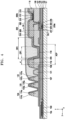
- the protective conductive layer 116 may cover the entire portion of the common voltage supply line 220 exposed through the first opening OP1 of the first insulating layer. Accordingly, an end of the protective conductive layer 116 towards the edge of the substrate 101 (in the +y direction) may be disposed on a top surface of the first insulating layer so that the protective conductive layer 116 reliably covers the portion of the common voltage supply line 220 exposed through the first opening OP1 of the first insulating layer.
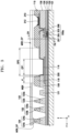
- the planarization layer 109 that may be referred to as a first insulating layer may cover the common voltage supply line 220 and may include the first opening OP1 through which a portion of a top surface of the common voltage supply line 220 is exposed.
- the protective conductive layer 116 covers the entire portion of the common voltage supply line 220 exposed through the first opening OP1 of the planarization layer 109, the end of the protective conductive layer 116 towards the edge of the substrate 101 (e.g., in the +y direction) may be disposed on a top surface of the planarization layer 109.
- a thin-film encapsulation layer 300 may cover the organic light-emitting element 200b.
- the thin-film encapsulation layer 300 may include at least one inorganic encapsulation layer and at least one organic encapsulation layer.
- the thin-film encapsulation layer 300 may include a first inorganic encapsulation layer 310, a second inorganic encapsulation layer 330, and an organic encapsulation layer 320 interposed between the first inorganic encapsulation layer 310 and the second inorganic encapsulation layer 330 (e.g., in the z direction).
- each of the first inorganic encapsulation layer 310 and the second inorganic encapsulation layer 330 may include at least one inorganic insulating material such as silicon oxide (SiO 2 ), silicon nitride (SiN x ), silicon oxynitride (SiO x N y ), aluminum oxide (Al 2 O 3 ), titanium oxide (TiO 2 ), tantalum oxide (Ta 2 O 5 ), hafnium oxide (HfO 2 ), or zinc oxide (ZnO 2 ), and may be formed by using chemical vapor deposition (CVD) or the like.
- the organic encapsulation layer 320 may include a polymer-based material.
- polymer-based material may include a silicone-based resin, an acrylic resin (e.g., polymethyl methacrylate or polyacrylic acid), an epoxy resin, polyimide, and polyethylene.
- acrylic resin e.g., polymethyl methacrylate or polyacrylic acid
- epoxy resin e.g., polyimide
- polyethylene e.g., polyethylene
- embodiments of the present disclosure are not necessarily limited thereto.
- Each of the first inorganic encapsulation layer 310, the organic encapsulation layer 320, and the second inorganic encapsulation layer 330 may be integrally formed to cover the display area DA.
- the dams 121, 122, 123, and 124 may be located in the peripheral area PA and may define a portion where a material for forming the organic encapsulation layer 320 of the thin-film encapsulation layer 300 is located when the organic encapsulation layer 320 of the thin-film encapsulation layer 300 is formed.
- the dams 121, 122, 123, and 124 may have a shape surrounding the display area DA in a plan view (e.g., in the x and/or y directions).
- the dams 121, 122, 123, and 124 may be spaced apart from each other in a plan view (e.g., in the x and/or y directions).
- the dams 121, 122, 123, and 124 may have various layer structures.
- the dam 121 may have a single-layer structure, and each of the dams 122, 123, and 124 may have a multi-layer structure.
- each of the dams 121, 122, 123, and 124 has a two-layer structure.
- Lower layers 122a, 123a, and 124a of the dams 122, 123, and 124 and the dam 121 may include, for example, the same material and the same layer structure as the planarization layer 109.
- the lower layers 122a, 123a, and 124a of the dams 122, 123, and 124, the dam 121, and the planarization layer 109 are formed simultaneously by using the same material.
- upper layers 122b, 123b, and 124b of the dams 122, 123, and 124 may include the same material and may have the same layer structure as the pixel-defining film 119.
- the upper layers 122b, 123b, and 124b of the dams 122, 123, and 124 and the pixel-defining film 119 are simultaneously formed by using the same material.
- the first transmission line 103 and/or the second transmission line 105 may have a shape extending along the edge of the substrate 101 in the peripheral area PA.
- the first transmission line 103 and the second transmission line 105 may transmit a common voltage to the common voltage supply line 220.
- a display apparatus that may prevent or reduce defects from occurring during a manufacturing process and an electronic apparatus including the display apparatus may be provided.
- the scope of embodiments of the present disclosure is not limited by this effect.
Landscapes
- Engineering & Computer Science (AREA)
- Microelectronics & Electronic Packaging (AREA)
- Manufacturing & Machinery (AREA)
- Devices For Indicating Variable Information By Combining Individual Elements (AREA)
- Electroluminescent Light Sources (AREA)
Applications Claiming Priority (1)
| Application Number | Priority Date | Filing Date | Title |
|---|---|---|---|
| KR1020230197606A KR20250105864A (ko) | 2023-12-29 | 2023-12-29 | 디스플레이 장치 |
Publications (1)
| Publication Number | Publication Date |
|---|---|
| EP4580366A1 true EP4580366A1 (de) | 2025-07-02 |
Family
ID=93926077
Family Applications (1)
| Application Number | Title | Priority Date | Filing Date |
|---|---|---|---|
| EP24220817.1A Pending EP4580366A1 (de) | 2023-12-29 | 2024-12-17 | Anzeigevorrichtung und elektronische vorrichtung damit |
Country Status (4)
| Country | Link |
|---|---|
| US (1) | US20250221195A1 (de) |
| EP (1) | EP4580366A1 (de) |
| KR (1) | KR20250105864A (de) |
| CN (1) | CN120282672A (de) |
Citations (1)
| Publication number | Priority date | Publication date | Assignee | Title |
|---|---|---|---|---|
| US20210066419A1 (en) * | 2019-09-04 | 2021-03-04 | Samsung Display Co., Ltd. | Display device and method of manufacturing the same |
-
2023
- 2023-12-29 KR KR1020230197606A patent/KR20250105864A/ko active Pending
-
2024
- 2024-08-02 US US18/792,654 patent/US20250221195A1/en active Pending
- 2024-12-12 CN CN202411824761.9A patent/CN120282672A/zh active Pending
- 2024-12-17 EP EP24220817.1A patent/EP4580366A1/de active Pending
Patent Citations (1)
| Publication number | Priority date | Publication date | Assignee | Title |
|---|---|---|---|---|
| US20210066419A1 (en) * | 2019-09-04 | 2021-03-04 | Samsung Display Co., Ltd. | Display device and method of manufacturing the same |
Also Published As
| Publication number | Publication date |
|---|---|
| CN120282672A (zh) | 2025-07-08 |
| KR20250105864A (ko) | 2025-07-09 |
| US20250221195A1 (en) | 2025-07-03 |
Similar Documents
| Publication | Publication Date | Title |
|---|---|---|
| US11088232B2 (en) | Display device | |
| US11882738B2 (en) | Display device with dam and driving circuit portions disposed on peripheral area | |
| US11770968B2 (en) | Display device with opening pattern | |
| US12369461B2 (en) | Display apparatus and method of manufacturing the same | |
| CN113299694B (zh) | 显示设备和柔性显示设备 | |
| US11581376B2 (en) | Method of manufacturing display apparatus | |
| US12002821B2 (en) | Display apparatus and method of manufacturing the same | |
| US11877477B2 (en) | Organic light-emitting display apparatus | |
| US11495650B2 (en) | Display apparatus | |
| US20210257433A1 (en) | Display device | |
| US20230032621A1 (en) | Display apparatus | |
| KR102927099B1 (ko) | 디스플레이 장치 및 그 제조 방법 | |
| CN112151579A (zh) | 显示设备和制造显示设备的方法 | |
| US12063817B2 (en) | Display apparatus and method of manufacturing the same | |
| US11502139B2 (en) | Display device and method of manufacturing the same | |
| US12207500B2 (en) | Organic light-emitting display apparatus | |
| EP4580366A1 (de) | Anzeigevorrichtung und elektronische vorrichtung damit | |
| US20240065051A1 (en) | Display device | |
| US20230105289A1 (en) | Display apparatus and method of providing the same | |
| EP4415504A1 (de) | Anzeigevorrichtung und verfahren zur herstellung davon | |
| US20250311548A1 (en) | Display apparatus and method of manufacturing the same | |
| US20230371317A1 (en) | Display apparatus | |
| US20230389362A1 (en) | Display apparatus and method of manufacturing the same |
Legal Events
| Date | Code | Title | Description |
|---|---|---|---|
| PUAI | Public reference made under article 153(3) epc to a published international application that has entered the european phase |
Free format text: ORIGINAL CODE: 0009012 |
|
| STAA | Information on the status of an ep patent application or granted ep patent |
Free format text: STATUS: THE APPLICATION HAS BEEN PUBLISHED |
|
| AK | Designated contracting states |
Kind code of ref document: A1 Designated state(s): AL AT BE BG CH CY CZ DE DK EE ES FI FR GB GR HR HU IE IS IT LI LT LU LV MC ME MK MT NL NO PL PT RO RS SE SI SK SM TR |
|
| STAA | Information on the status of an ep patent application or granted ep patent |
Free format text: STATUS: REQUEST FOR EXAMINATION WAS MADE |
|
| 17P | Request for examination filed |
Effective date: 20251217 |
|
| P01 | Opt-out of the competence of the unified patent court (upc) registered |
Free format text: CASE NUMBER: UPC_APP_0007604_4580366/2026 Effective date: 20260226 |