EP4580362A1 - Transparente anzeigevorrichtung - Google Patents
Transparente anzeigevorrichtung Download PDFInfo
- Publication number
- EP4580362A1 EP4580362A1 EP24197915.2A EP24197915A EP4580362A1 EP 4580362 A1 EP4580362 A1 EP 4580362A1 EP 24197915 A EP24197915 A EP 24197915A EP 4580362 A1 EP4580362 A1 EP 4580362A1
- Authority
- EP
- European Patent Office
- Prior art keywords
- pixel
- sub
- disposed
- pixels
- red
- Prior art date
- Legal status (The legal status is an assumption and is not a legal conclusion. Google has not performed a legal analysis and makes no representation as to the accuracy of the status listed.)
- Pending
Links
Images




Classifications
-
- H—ELECTRICITY
- H10—SEMICONDUCTOR DEVICES; ELECTRIC SOLID-STATE DEVICES NOT OTHERWISE PROVIDED FOR
- H10K—ORGANIC ELECTRIC SOLID-STATE DEVICES
- H10K59/00—Integrated devices, or assemblies of multiple devices, comprising at least one organic light-emitting element covered by group H10K50/00
- H10K59/30—Devices specially adapted for multicolour light emission
- H10K59/35—Devices specially adapted for multicolour light emission comprising red-green-blue [RGB] subpixels
- H10K59/353—Devices specially adapted for multicolour light emission comprising red-green-blue [RGB] subpixels characterised by the geometrical arrangement of the RGB subpixels
-
- H—ELECTRICITY
- H10—SEMICONDUCTOR DEVICES; ELECTRIC SOLID-STATE DEVICES NOT OTHERWISE PROVIDED FOR
- H10K—ORGANIC ELECTRIC SOLID-STATE DEVICES
- H10K59/00—Integrated devices, or assemblies of multiple devices, comprising at least one organic light-emitting element covered by group H10K50/00
- H10K59/10—OLED displays
- H10K59/12—Active-matrix OLED [AMOLED] displays
-
- H—ELECTRICITY
- H10—SEMICONDUCTOR DEVICES; ELECTRIC SOLID-STATE DEVICES NOT OTHERWISE PROVIDED FOR
- H10K—ORGANIC ELECTRIC SOLID-STATE DEVICES
- H10K59/00—Integrated devices, or assemblies of multiple devices, comprising at least one organic light-emitting element covered by group H10K50/00
- H10K59/10—OLED displays
- H10K59/12—Active-matrix OLED [AMOLED] displays
- H10K59/121—Active-matrix OLED [AMOLED] displays characterised by the geometry or disposition of pixel elements
-
- H—ELECTRICITY
- H10—SEMICONDUCTOR DEVICES; ELECTRIC SOLID-STATE DEVICES NOT OTHERWISE PROVIDED FOR
- H10K—ORGANIC ELECTRIC SOLID-STATE DEVICES
- H10K59/00—Integrated devices, or assemblies of multiple devices, comprising at least one organic light-emitting element covered by group H10K50/00
- H10K59/10—OLED displays
- H10K59/12—Active-matrix OLED [AMOLED] displays
- H10K59/131—Interconnections, e.g. wiring lines or terminals
-
- H—ELECTRICITY
- H10—SEMICONDUCTOR DEVICES; ELECTRIC SOLID-STATE DEVICES NOT OTHERWISE PROVIDED FOR
- H10K—ORGANIC ELECTRIC SOLID-STATE DEVICES
- H10K59/00—Integrated devices, or assemblies of multiple devices, comprising at least one organic light-emitting element covered by group H10K50/00
- H10K59/30—Devices specially adapted for multicolour light emission
- H10K59/35—Devices specially adapted for multicolour light emission comprising red-green-blue [RGB] subpixels
- H10K59/351—Devices specially adapted for multicolour light emission comprising red-green-blue [RGB] subpixels comprising more than three subpixels, e.g. red-green-blue-white [RGBW]
-
- H—ELECTRICITY
- H10—SEMICONDUCTOR DEVICES; ELECTRIC SOLID-STATE DEVICES NOT OTHERWISE PROVIDED FOR
- H10K—ORGANIC ELECTRIC SOLID-STATE DEVICES
- H10K71/00—Manufacture or treatment specially adapted for the organic devices covered by this subclass
- H10K71/861—Repairing
-
- G—PHYSICS
- G09—EDUCATION; CRYPTOGRAPHY; DISPLAY; ADVERTISING; SEALS
- G09G—ARRANGEMENTS OR CIRCUITS FOR CONTROL OF INDICATING DEVICES USING STATIC MEANS TO PRESENT VARIABLE INFORMATION
- G09G2300/00—Aspects of the constitution of display devices
- G09G2300/04—Structural and physical details of display devices
- G09G2300/0439—Pixel structures
- G09G2300/0443—Pixel structures with several sub-pixels for the same colour in a pixel, not specifically used to display gradations
-
- G—PHYSICS
- G09—EDUCATION; CRYPTOGRAPHY; DISPLAY; ADVERTISING; SEALS
- G09G—ARRANGEMENTS OR CIRCUITS FOR CONTROL OF INDICATING DEVICES USING STATIC MEANS TO PRESENT VARIABLE INFORMATION
- G09G2320/00—Control of display operating conditions
- G09G2320/02—Improving the quality of display appearance
- G09G2320/0233—Improving the luminance or brightness uniformity across the screen
-
- G—PHYSICS
- G09—EDUCATION; CRYPTOGRAPHY; DISPLAY; ADVERTISING; SEALS
- G09G—ARRANGEMENTS OR CIRCUITS FOR CONTROL OF INDICATING DEVICES USING STATIC MEANS TO PRESENT VARIABLE INFORMATION
- G09G2320/00—Control of display operating conditions
- G09G2320/04—Maintaining the quality of display appearance
- G09G2320/043—Preventing or counteracting the effects of ageing
- G09G2320/045—Compensation of drifts in the characteristics of light emitting or modulating elements
-
- G—PHYSICS
- G09—EDUCATION; CRYPTOGRAPHY; DISPLAY; ADVERTISING; SEALS
- G09G—ARRANGEMENTS OR CIRCUITS FOR CONTROL OF INDICATING DEVICES USING STATIC MEANS TO PRESENT VARIABLE INFORMATION
- G09G2330/00—Aspects of power supply; Aspects of display protection and defect management
- G09G2330/02—Details of power systems and of start or stop of display operation
- G09G2330/021—Power management, e.g. power saving
-
- G—PHYSICS
- G09—EDUCATION; CRYPTOGRAPHY; DISPLAY; ADVERTISING; SEALS
- G09G—ARRANGEMENTS OR CIRCUITS FOR CONTROL OF INDICATING DEVICES USING STATIC MEANS TO PRESENT VARIABLE INFORMATION
- G09G3/00—Control arrangements or circuits, of interest only in connection with visual indicators other than cathode-ray tubes
- G09G3/20—Control arrangements or circuits, of interest only in connection with visual indicators other than cathode-ray tubes for presentation of an assembly of a number of characters, e.g. a page, by composing the assembly by combination of individual elements arranged in a matrix no fixed position being assigned to or needed to be assigned to the individual characters or partial characters
- G09G3/22—Control arrangements or circuits, of interest only in connection with visual indicators other than cathode-ray tubes for presentation of an assembly of a number of characters, e.g. a page, by composing the assembly by combination of individual elements arranged in a matrix no fixed position being assigned to or needed to be assigned to the individual characters or partial characters using controlled light sources
- G09G3/30—Control arrangements or circuits, of interest only in connection with visual indicators other than cathode-ray tubes for presentation of an assembly of a number of characters, e.g. a page, by composing the assembly by combination of individual elements arranged in a matrix no fixed position being assigned to or needed to be assigned to the individual characters or partial characters using controlled light sources using electroluminescent panels
- G09G3/32—Control arrangements or circuits, of interest only in connection with visual indicators other than cathode-ray tubes for presentation of an assembly of a number of characters, e.g. a page, by composing the assembly by combination of individual elements arranged in a matrix no fixed position being assigned to or needed to be assigned to the individual characters or partial characters using controlled light sources using electroluminescent panels semiconductive, e.g. using light-emitting diodes [LED]
- G09G3/3208—Control arrangements or circuits, of interest only in connection with visual indicators other than cathode-ray tubes for presentation of an assembly of a number of characters, e.g. a page, by composing the assembly by combination of individual elements arranged in a matrix no fixed position being assigned to or needed to be assigned to the individual characters or partial characters using controlled light sources using electroluminescent panels semiconductive, e.g. using light-emitting diodes [LED] organic, e.g. using organic light-emitting diodes [OLED]
- G09G3/3225—Control arrangements or circuits, of interest only in connection with visual indicators other than cathode-ray tubes for presentation of an assembly of a number of characters, e.g. a page, by composing the assembly by combination of individual elements arranged in a matrix no fixed position being assigned to or needed to be assigned to the individual characters or partial characters using controlled light sources using electroluminescent panels semiconductive, e.g. using light-emitting diodes [LED] organic, e.g. using organic light-emitting diodes [OLED] using an active matrix
- G09G3/3233—Control arrangements or circuits, of interest only in connection with visual indicators other than cathode-ray tubes for presentation of an assembly of a number of characters, e.g. a page, by composing the assembly by combination of individual elements arranged in a matrix no fixed position being assigned to or needed to be assigned to the individual characters or partial characters using controlled light sources using electroluminescent panels semiconductive, e.g. using light-emitting diodes [LED] organic, e.g. using organic light-emitting diodes [OLED] using an active matrix with pixel circuitry controlling the current through the light-emitting element
-
- H—ELECTRICITY
- H10—SEMICONDUCTOR DEVICES; ELECTRIC SOLID-STATE DEVICES NOT OTHERWISE PROVIDED FOR
- H10K—ORGANIC ELECTRIC SOLID-STATE DEVICES
- H10K59/00—Integrated devices, or assemblies of multiple devices, comprising at least one organic light-emitting element covered by group H10K50/00
- H10K59/30—Devices specially adapted for multicolour light emission
- H10K59/38—Devices specially adapted for multicolour light emission comprising colour filters or colour changing media [CCM]
-
- H—ELECTRICITY
- H10—SEMICONDUCTOR DEVICES; ELECTRIC SOLID-STATE DEVICES NOT OTHERWISE PROVIDED FOR
- H10K—ORGANIC ELECTRIC SOLID-STATE DEVICES
- H10K59/00—Integrated devices, or assemblies of multiple devices, comprising at least one organic light-emitting element covered by group H10K50/00
- H10K59/80—Constructional details
- H10K59/8791—Arrangements for improving contrast, e.g. preventing reflection of ambient light
- H10K59/8792—Arrangements for improving contrast, e.g. preventing reflection of ambient light comprising light absorbing layers, e.g. black layers
Definitions
- the present disclosure relates to a transparent display apparatus.
- LCD liquid crystal display
- PDP plasma display panel
- QLED quantum dot light emitting display
- OLED organic light emitting display
- the transparent display apparatus may include a display area on which an image is displayed and a non-display area, and the display area may include a transmissive area capable of transmitting external light and a light emission area. he transparent display apparatus may have a high light transmittance in the display area through the transmissive area.
- one sub-pixel is divided into a plurality of sub-pixels in the display area, and the plurality of divided sub-pixels are connected to thin-film transistors through repair wiring.
- the repair wiring connected to the sub-pixel in which the dark point occurs may be cut so that the remaining sub-pixels may be operated normally.
- the transparent display apparatus has a problem that the repair wiring connecting the plurality of divided sub-pixels is disposed in the transmissive area, thus the transmissivity of the transmissive area is reduced.
- the present disclosure is directed to a transparent display apparatus that substantially obviates one or more of problems due to limitations and disadvantages described above.
- the present disclosure is to provide a transparent display apparatus capable of improving the transmissivity of a transmissive portion.
- the present disclosure is also to provide a transparent display apparatus in which overall power consumption may be reduced.
- the present disclosure is to provide a transparent display apparatus in which reduced visibility due to diffraction phenomenon may be prevented.
- a transparent display apparatus includes a first pixel disposed on a substrate and having a plurality of first sub-pixels and a plurality of transmissive portions, a second pixel adj acent to the first pixel and having a plurality of second sub-pixels and a plurality of transmissive portions, and a third pixel adjacent to the first pixel and the second pixel and having a plurality of third sub-pixels and a plurality of transmissive portions, wherein one first sub-pixel of the plurality of first sub-pixels, one second sub-pixel of the plurality of second sub-pixels, and one third sub-pixel of the plurality of third sub-pixels are disposed adjacent to each other.
- a transparent display apparatus includes a plurality of pixels disposed on a substrate, each of the plurality pixels including a plurality of sub-pixels and a plurality of transmissive portions; and a wiring for driving the plurality of sub-pixels, wherein the plurality of sub-pixels includes two sub-pixels disposed in a first direction and two sub-pixels disposed in a second direction, so that the plurality of sub-pixels is disposed in an X shape in each pixel, wherein the transmissive portions are disposed between every two sub-pixels of the plurality of sub-pixels, and wherein the wiring partially overlaps the plurality of sub-pixels without overlapping the transmissive portions.
- X-axis direction should not be construed by a geometric relation only of a mutual vertical relation and may have broader directionality within the range that elements of the present disclosure may act functionally.
- At least one should be understood as including any and all combinations of one or more of the associated listed items.
- the meaning of "at least one of a first item, a second item and a third item” denotes the combination of all items proposed from two or more of the first item, the second item and the third item as well as the first item, the second item or the third item.
- FIG. 1 is a plan view schematically illustrating a transparent display apparatus according to one aspect of the present disclosure.
- the X-axis represents a horizontal direction (i.e., a length direction) of the transparent display apparatus with respect to FIG. 1
- the Y-axis represents a perpendicular direction (i.e., a width direction) of the transparent display apparatus with respect to FIG. 1
- the first direction D1 represents a first diagonal direction (i.e., a first diagonal direction of a pixel) intersecting the X-axis and Y-axis
- the second direction D2 represents a second diagonal direction (a diagonal direction of a pixel) orthogonal to the first diagonal direction
- the Z-axis represents a thickness (or height) direction of the transparent display apparatus 100.
- the transparent display apparatus 100 has been described as an organic light emitting display, but the transparent display apparatus 100 may also be implemented as a liquid crystal display, a plasma display panel (PDP), a quantum dot light emitting display (QLED), or an electrophoresis display.
- the transparent display apparatus 100 may also be implemented as a liquid crystal display, a plasma display panel (PDP), a quantum dot light emitting display (QLED), or an electrophoresis display.
- a transparent display apparatus 100 may include a transparent display panel, a source drive integrated circuit (hereinafter IC) 120, a flexible film 130, a circuit boards 140, and a timing controller 150.
- IC source drive integrated circuit
- the transparent display panel includes a substrate 110 and an opposing substrate 200 (shown in FIG. 4 ), that face each other.
- the substrate 110 may be a plastic film, a glass substrate, or a silicon wafer substrate formed using a semiconductor process.
- the opposing substrate 200 may be a plastic film, a glass substrate, or an encapsulation film. Such substrate 110 and opposing substrate 200 may be made of a transparent material.
- the substrate 110 may include a display area DA and a non-display area NDA.
- the display area DA is an area where an image is displayed, and may be a pixel array area, an active area, a pixel array unit, a display unit, or a screen.
- the display area DA may be disposed at a central portion of the display panel.
- the display area DA may include a plurality of pixels P.
- the non-display area NDA may be an area where an image is not displayed, and may be a peripheral area, a signal supply area, a non-active area, or a bezel area.
- the non-display area NDA may be configured to be around the display area DA. That is, the non-display area NDA may be disposed to surround the display area DA.
- a pad portion PA may be disposed in the non-display area NDA.
- the pad portion PA may supply power and/or signals for outputting images to the pixels P provided in the display area DA.
- the pad portion PA may be provided on the upper side of the display area DA.
- Pads such as power pads, data pads, may be formed in the non-display area of the substrate 110.
- Lines connecting the pads with the source drive IC 120 and lines connecting the pads with lines of the circuit board 140 may be formed in the flexible film 130.
- the flexible film 130 may be attached onto the pads by using an anisotropic conducting film, whereby the pads may be connected with the lines of the flexible film 130.
- a gate driver GD may be formed in a Gate driver In Panel (GIP) manner on the non-display area NDA outside one or both sides of the display area DA of the substrate 110.
- the gate driver may be fabricated as a drive chip, mounted on a flexible film, and attached to the non-display area NDA on one side or both sides outside of the display area DA of the substrate 110 in a Tape Automated Bonding (TAB) manner.
- GIP Gate driver In Panel
- TAB Tape Automated Bonding
- the circuit board 140 may be attached to the flexible films 130.
- a plurality of circuits implemented as driving chips may be packaged in the circuit board 140.
- the timing controller 150 may be packaged in the circuit board 140.
- the circuit board 140 may be a printed circuit board or a flexible printed circuit board.
- the timing controller 150 receives the digital video data and a timing signal from an external system board through a cable of the circuit board 140.
- the timing controller 150 generates a gate control signal for controlling an operation timing of the gate driver GD and a source control signal for controlling the source drive ICs 120 based on the timing signal.
- the timing controller 150 supplies the gate control signal to the gate driver GD, and supplies the source control signal to the source drive ICs 120.
- FIG. 2 is an enlarged view of A portion in FIG. 1
- FIG. 3 is a diagram illustrating an example arrangement of a plurality of signal lines and a plurality of transistors
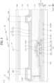
- FIG. 4 is a cross-sectional view illustrating one example of I-I' of FIG. 3 .
- the substrate 110 may include the light emission area EA and the non-light emission area NEA.
- the light emission area EA may mean an area from which light is emitted.
- a light emitting element layer E which includes a pixel electrode 114, an organic light emitting layer 116 and an opposing electrode 117, may be disposed in the light emission area EA. When an electric field is formed between the pixel electrode 114 and the opposing electrode 117, the organic light emitting layer 116 in the light emission area EA may be emitted.
- a first green sub-pixel SP1-2 included in the plurality of first sub-pixels SP1 may be disposed adjacent to a second blue sub-pixel SP2-3 included in the plurality of second sub-pixels SP2, and a third white sub-pixel SP3-4 included in a plurality of third sub-pixels SP3.
- one second sub-pixel SP2 included in the second pixel P2, and one third sub-pixel SP3 included in the third pixel P3 are disposed adjacent to one first sub-pixel SP1 included in the first pixel P1 is that when a dark point occurs in one first sub-pixel SP1 included in the first pixel P1, one second sub-pixel SP2 included in the second pixel P2 and one third sub-pixel SP3 included in the third pixel P3 are emitting light to prevent that the user recognizes the first sub-pixel SP1 in which the dark point has occurred. In other words, the more shared sub-pixels there are, the less visible the dark point is.
- one first sub-pixel SP1 included in the first pixel P1, one second sub-pixel SP2 included in the second pixel P2, and one third sub-pixel SP3 included in the third pixel P3 may all be sub-pixels that emit the same color.
- three sub-pixels SPs emitting different colors of light are disposed adjacent to each other. This is because the other two sub-pixels SPs emit the same color of light as the color of light emitted by the sub-pixel where the dark point occurred is disposed as close as possible to the sub-pixel where the dark point occurred, compared to the other sub-pixels emitting different colors of light. Therefore, the other two sub-pixels emits the same color of light at as close as possible to the sub-pixel where the dark point occurred, thus the user's perception of the dark point may be minimized.
- the transparent display apparatus 100 may have a feature that one first sub-pixel SP1 (e. g., a first green sub-pixel SP1-2), one second sub-pixel SP2 (e. g., a second blue sub-pixel SP2-3), and one third sub-pixel SP3 (e. g., a third white sub-pixel SP3-4), which are disposed adjacent to each other, emit a different color of light from each other.
- one first sub-pixel SP1 e. g., a first green sub-pixel SP1-2
- one second sub-pixel SP2 e. g., a second blue sub-pixel SP2-3
- third sub-pixel SP3 e. g., a third white sub-pixel SP3-4
- the plurality of first sub-pixels SP1 includes a first red sub-pixel SP1-1, a first green sub-pixel SP1-2, a first blue sub-pixel SP1-3, and a first white sub-pixel SP1-4.
- the first red sub-pixel SP1-1 is disposed in the first direction D1.
- the first green sub-pixel SP1-2 is disposed adjacent to the first red sub-pixel SP1-1 and disposed in the first direction D1.
- the first blue sub-pixel SP1-3 is disposed partially adjacent to each of one side of the first red sub-pixel SP1-1 and one side of the first green sub-pixel SP1-2 and disposed in the second direction D2.
- the first white sub-pixel SP1-4 is disposed partially adjacent to each of the other side of the first red sub-pixel SP1-1 and the other side of the first green sub-pixel SP1-2 and disposed in the second direction D2.
- the one side of the first red sub-pixel SP1-1 may refer to a left lower side of the first red sub-pixel SP1-1 with respect to FIG. 2 .
- the other side of the first red sub-pixel SP1-1 may refer to a right upper side of the first red sub-pixel SP1-1 with respect to FIG. 2 .
- the first red sub-pixel SP1-1, the first green sub-pixel SP1-2, the first blue sub-pixel SP1-3, and the first white sub-pixel SP1-4 may be disposed in a windmill shape or an X shape.
- the plurality of second sub-pixels SP2 includes a second red sub-pixel SP2-1, a second green sub-pixel SP2-2, a second blue sub-pixel SP2-3, and a second white sub-pixel SP2-4.
- the second red sub-pixel SP2-1 is disposed in the first direction D1.
- the second green sub-pixel SP2-2 is disposed adjacent to the second red sub-pixel SP2-1 and disposed in the first direction D1.
- the second blue sub-pixel SP2-3 is disposed partially adjacent to each of one side of the second red sub-pixel SP2-1 and one side of the second green sub-pixel SP2-2, and disposed in a second direction D2.
- the second white sub-pixel SP2-4 is disposed partially adjacent to each of the other side of the second red sub-pixel SP2-1 and the other side of the second green sub-pixel SP2-2 and disposed in the second direction D2.
- One side of the second red sub-pixel SP1-1 may refer to a left lower side of the second red sub-pixel SP2-1 with respect to FIG. 2 .
- the other side of the second red sub-pixel SP2-1 may refer a right upper side of the second red sub-pixel SP2-1 with respect to FIG. 2 .
- the second red sub-pixel SP2-1, the second green sub-pixel SP2-2, the second blue sub-pixel SP2-3, and the second white sub-pixel SP2-4 may be disposed in a windmill shape or an X shape.
- each of the plurality of first sub-pixels SP1 and the plurality of second sub-pixels SP2 may be disposed in a windmill shape, thus the first green sub-pixel SP1-2 may be disposed adjacent to the second blue sub-pixel SP2-3, and the first white sub-pixel SP1-4 may be disposed adjacent to the second red sub-pixel SP2-1.
- the plurality of third sub-pixels SP3 includes a third red sub-pixel SP3-1, a third green sub-pixel SP3-2, a third blue sub-pixel SP3-3, and a third white sub-pixel SP3-4.
- the third red sub-pixel SP3-1 is disposed in the first direction D1.
- the third green sub-pixel SP3-2 is disposed adjacent to the third red sub-pixel SP3-1 and disposed in the first direction D1.
- the third blue sub-pixel SP3-3 is disposed partially adjacent to each of one side of the third red sub-pixel SP3-1 and one side of the third green sub-pixel SP3-2 and disposed in the second direction D2.
- the third white sub-pixel SP3-4 is disposed partially adjacent to each of the other side of the third red sub-pixel SP3-1 and the other side of the third green sub-pixel SP3-2 and disposed in the second direction D2.
- One side of the third red sub-pixel SP3-1 may refer to a left lower side of the third red sub-pixel SP3-1 with respect to FIG. 2 .
- the other side of the third red sub-pixel SP3-1 may refer a right upper side of the third red sub-pixel SP3-1 with respect to FIG. 2 .
- the third red sub-pixel SP3-1, the third green sub-pixel SP3-2, the third blue sub-pixel SP3-3, and the third white sub-pixel SP3-4 may be disposed in a windmill shape or an X shape.
- each of the plurality of first sub-pixels SP1 and the plurality of third sub-pixels SP3 may be disposed in a windmill shape, thus the first green sub-pixel SP1-2 is disposed adjacent to the third white sub-pixel SP3-4, and the first blue sub-pixel SP1-3 is disposed adjacent to the third red sub-pixel SP3-1.
- the transparent display apparatus 100 may be configured to emit the second sub-pixel SP2 of the same color and the third sub-pixel SP3 of the same color when one first sub-pixel SP1 of the plurality of first sub-pixels SP1 is a sub-pixel where the dark point occurred, thus the first sub-pixel SP1 where the dark point occurred may be minimized or prevented from being perceived by a user.
- the transparent display apparatus 100 may drive the same-colored sub-pixels of two other adjacent pixels in place of the sub-pixel where the dark point occurred, thus the image to be expressed in a particular pixel may be expressed using the adjacent pixels.
- the driving method mentioned above is defined herein as visual rendering driving.
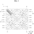
- the transparent display apparatus 100 may drive the same-colored sub-pixels of the other two adjacent pixels in place of the sub-pixel where the dark point occurred, thus the user's perceptibility of the sub-pixel where the dark point occurred may be minimized. This will be described further in connection with FIG. 5 .
- one pixel P1 included in the transparent display apparatus 100 will be described in detail.
- the first pixel P1 may include the plurality of first sub-pixels SP1.
- the plurality of first sub-pixels SP1 may include the first red sub-pixel SP1-1 and the first green sub-pixel SP1-2, the first blue sub-pixel SP1-3 and the first white sub-pixel SP1-4.
- the first red sub-pixel SP1-1 and the first green sub-pixel SP1-2 are disposed adjacent each other in the first direction D1, and the first blue sub-pixel SP1-3 and the first white sub-pixel SP1-4 are disposed adjacent in the second direction D2.
- the first blue sub-pixel SP1-3 may be disposed partially adjacent to each of one side of the first red sub-pixel SP1-1 and the first green sub-pixel SP1-2.
- the first white sub-pixel SP1-4 may be disposed partially adjacent to each of the other side of the first red sub-pixel SP1-1 and the other side of the first green sub-pixel SP1-2.
- the first red sub-pixel SP1-1, the first green sub-pixel SP1-2, the first blue sub-pixel SP1-3, and the first white sub-pixel SP1-4 may be disposed in a windmill shape or an X shape.
- the scan transistors R3, G3, B3, W3 is switched according to the scan signal supplied to the gate line GL (or scan line GL) to supply the data voltage supplied from the data lines DL1, DL2, DL3, DL4 to the drive transistors R1, G1, B1, W1.
- the drive transistors R1, G1, B1, W1 are switched according to the data voltage supplied from the scan transistor to generate a data current from the power supplied from the pixel power line EVDD and supply it to the pixel electrodes 114 of the sub-pixel.
- Each of the drive transistors R1, G1, B1, and W1 (or drive transistor 112) includes an active layer 112a, a gate electrode 112b, a source electrode 112c, and a drain electrode 112d.
- the capacitors R2, G2, B2, W2 maintain the data voltage supplied to the drive transistors R1, G1, B1, W1 (or 112) for one frame.
- Each of the capacitors R2, G2, B2, W2 may include a first capacitor electrode and a second capacitor electrode.
- a light-shielding layer LS may be provided between the active layer 112a and the first substrate 110.
- the light-shielding layer LS may serve as a light shielding layer for shielding external light entering the active layer 112a.
- the light-shielding layer LS may be made of a conductive material.
- the light-shielding layer LS may be formed of a single layer or a multi-layer made of one of Mo, Al, Cr, Au, Ti, Ni, Nd and Cu, or their alloy.
- a buffer layer BL may be provided between the light-shielding layer LS and the active layer 112a.
- a gate insulating layer 111a may be provided over the active layer 112a.
- the gate insulating layer 111a may be formed of an inorganic film such as a silicon oxide film (SiOx) and a silicon nitride film (SiNx) or a multi-layered film of SiOx and SiNx.
- the gate electrode 112b may be provided over the gate insulating layer 111a.
- the gate electrode 112b may be formed of a single layer or a multi-layer made of any one of Mo, Al, Cr, Au, Ti, Ni, Nd and Cu, or their alloy.
- An inter-layer dielectric layer 111b may be provided over the gate electrode 112b.
- the inter-layer dielectric layer 111b may be made of an inorganic film such as a silicon oxide film (SiOx) and a silicon nitride film (SiNx) or a multi-layered film of SiOx and SiNx.
- the source electrode 112c SE and the drain electrode 112d may be provided over the inter-layer dielectric layer 111b.
- the source electrode 112c and the drain electrode 112d may be connected to the active layer 112a through a contact hole passing through the gate insulating layer 111a and the inter-layer dielectric layer 111b.
- the first passivation layer 111c may be provided on the source electrode 112c and the drain electrode 112d to protect the drive transistors R1, G1, B1, W1 (or 112).
- the first passivation layer 111c may be disposed between the substrate 110 and the planarization layer 113.
- the first passivation layer 111c covers the drain electrode 112d and the source electrode 112c of the drive transistor 112 and the interlayer insulating layer 111b.
- the first passivation layer 111c may be formed throughout the circuit area and the light emission area EA.
- a second passivation layer 111d may be disposed on the substrate 110 to cover a pixel P.
- the second passivation layer 111d may be disposed between the first passivation layer 111c and the planarization layer 113 to cover the connection electrode CE.
- the second passivation layer 111d may be formed throughout the circuit region and the light emission area EA.
- the connection electrode CE according to one example may be clad.
- the planarization layer 113 may be provided on the second passivation layer 111d for planarizing a step difference caused by the drive transistors R1, G1, B1, W1 (or 112).
- the planarization layer 113 may be formed of an organic film such as an acrylic resin, an epoxy resin, a phenolic resin, a polyamide resin, a polyimide resin, or the like.
- the gate insulating layer 111a, the interlayer insulating layer 11 1b, the first passivation layer 111c, and the second passivation layer 111d may be included in an inorganic layer 111.
- the bank 115 and a light emitting elements comprising pixel electrodes 114, organic emitting layer 116, and opposing electrodes 117 is provided on the planarization layer 113.
- the pixel electrode 114 may be provided on the planarization layer 113 and connected to the drive transistors R1, G1, B1, W1, or 112 through the connection electrode CE. Specifically, the pixel electrode 114 may be connected to the source electrode 112c or the drain electrode 112d of the drive transistors R1, G1, B1, W1 (or 112) through the first contact hole CNT1 penetrating the planarization layer 113 and the second passivation layer 111d. Accordingly, the pixel electrodes 114 may be electrically connected to the drive transistors R1, G1, B1, W1 (or 112).
- Such pixel electrodes 114 may be provided for each of sub-pixels SP1-1, SP1-2, SP1-3, SP1-4.
- One pixel electrode 114 may be formed in the first red sub-pixel SP1-1
- another pixel electrode 114 may be formed in the first green sub-pixel SP1-2
- still another pixel electrode 114 may be formed in the first blue sub-pixel SP1-3
- yet another pixel electrode 114 may be formed in the first white sub-pixel SP1-4.
- the pixel electrode 114 is not provided in the transmissive portion TA (or the first to fourth transmissive portions TA1, TA2, TA3, TA4).
- the pixel electrode 114 may be formed of a metal material of high reflectivity such as a deposited structure (Ti /Al/Ti) of aluminum and titanium, a deposited structure (ITO/Al/ITO) of aluminum and ITO, an Ag alloy and a deposited structure (ITO/Ag alloy/ITO) of Ag alloy and ITO, MoTi alloy and a deposited structure (ITO/MoTi alloy/ITO) of MoTi alloy and ITO.
- the Ag alloy may be an alloy of silver (Ag), palladium (Pb), and Copper (Cu).
- the MoTi alloy may be an alloy of molybdenum (Mo) and titanium (Ti).
- the pixel electrode 114 may be an anode electrode or a first electrode.
- the one end of the first red sub-pixel SP1-1 may be provided in a protruding shape, and the other end of the first red sub-pixel SP1-1 may be provided in a shape different from the one end.
- the one end of the first red sub-pixel SP1-1 may be provided in a triangular shape, and the other end may be provided in a straight line shape.
- the one end of the first red sub-pixel SP1-1 may be a portion of the first red sub-pixel SP1-1 that is adjacent to a sub-pixel SP of another pixel P.
- the other end of the first red sub-pixel SP1-1 may be a portion of the first red sub-pixel SP1-1 that is adjacent to another sub-pixel SP of the same pixel P, for example, a portion of the first red sub-pixel SP1-1 that is adjacent to the first green sub-pixel SP1-2.
- the one end of the first red sub-pixel SP1-1 provided in a protruding shape is to be disposed adjacent to each of the protruding ends of the blue sub-pixel of another pixel, and the protruding ends of the white sub-pixel of another pixel. Since each of the sub-pixels having different colors is provided in a protruding shape, the sub-pixels of different pixels may be disposed in close proximity, thereby minimizing the size (or area) of the non-light emission area NEA where no light is emitted.
- each of the sub-pixels having a different color is provided in a protruding shape, sub-pixels having different colors may be disposed in close proximity, so that two sub-pixels having the same color may be emitted in close proximity to a sub-pixel where the dark point occurs, thereby minimizing the visibility of the dark point to the user.
- the transparent display apparatus 100 is configured such that when the dark point occurs in a sub-pixel SP included in one of the pixels P, the same-colored sub-pixel SP included in each of other two pixels P emits light via a visual rendering drive, thereby minimizing the perceptibility of the sub-pixel where the dark point occurs.
- the adjacent one sub-pixel has to emit up to the data value of the sub-pixel where the dark point occurs, which not only requires a high power but also causes a problem that the emitting sub-pixel is subjected to a high driving stress, which reduces the service life.
- the transparent display apparatus 100 is configured with at least two sub-pixels (or shared sub-pixels) emitting the same color as the sub-pixel where the dark point occurs, so that one sub-pixel (or one shared sub-pixel) may be driven at a lower power than in the case of a conventional transparent display apparatus in which only one sub-pixel of the same color is emitted, thereby reducing the overall power consumption, and minimizing or preventing the reduction in service life.
- the transparent display apparatus 100 is configured so that one end of the first red sub-pixel SP1-1 is provided in a protruding shape, and the other end of the first red sub-pixel SP1-1 is provided in a shape different from the one end. Accordingly, the sub-pixels of the different pixels may be disposed close together, the size (or area) of the non-light emission area NEA may be minimized, and the perceptibility of the sub-pixel where the dark point occurs may be minimized by driving the visual rendering when the dark point occurs, thereby providing a high quality image.
- the plurality of first sub-pixels SP1 may be disposed adjacent to each other while minimizing the size (or area) of the non-light emission area NEA, as shown in FIG. 3 .
- each of the first green sub-pixel SP1-2, the first blue sub-pixel SP1-3, and the first white sub-pixel SP1-4 that are included in the first pixel P1 has the same structure as the first red sub-pixel SP1-1, so a description of them will be omitted.
- the bank 115 may be provided on the planarization layer 113. Further, the banks 115 may be provided between the pixel electrodes 114 Also, the bank 115 may be formed such that it covers an edge of each of the pixel electrodes 114 and a portion of each of the pixel electrodes 114 is exposed. Accordingly, since the thickness of the organic light emitting layer 116 becomes thinner at each of the ends of the pixel electrodes 114, the bank 115 may prevent the pixel electrodes 114 and the opposing electrodes 117 from contacting.
- the bank 115 may define light emission areas EA1, EA2, EA3, EA4 for each of the first red sub-pixel SP1-1, the first green sub-pixel SP1-2, the first blue sub-pixel SP1-3, and the first white sub-pixel SP1-4.
- the light emission areas EA1, EA2, EA3, EA4 of each of the sub-pixels SP1-1, SP1-2, SP1-3, SP1-4 represent areas where the pixel electrode 114, the organic light emitting layer 116, and the opposing electrode 117 are stacked sequentially so that holes from the pixel electrode 114 and electrons from the opposing electrode 117 are combined with each other in the organic light emitting layer 116 and emit light.
- the area where the bank 115 is formed does not emit light and thus becomes the non-light emission area NEA, and the area where the bank 115 is not formed and the pixel electrode 114 is exposed may become the light emission area EA1, EA2, EA3, EA4.
- the non-light emission area NEA may refer to the area where a black matrix BM is disposed.
- the bank 115 may be formed of an organic layer, for example, acryl resin, epoxy resin, phenolic resin, polyamide resin, polyimide resin, etc.
- the organic light emitting layer 116 may be provided over the pixel electrode 114.
- the organic light emitting layer 116 may include a hole transporting layer, a light emitting layer, and an electron transporting layer. In this case, if a voltage is applied to the pixel electrode 114 and the opposing electrode 117, holes and electrons move to the light emitting layer through the hole transporting layer and the electron transporting layer, respectively, and are combined with each other in the light emitting layer to emit light.
- the organic light emitting layer 116 may be a common layer formed common to the first red sub-pixel SP1-1, the first green sub-pixel SP1-2, the first blue sub-pixel SP1-3, and the first white sub-pixel SP1-4.
- the light-emitting layer may be a white light-emitting layer that emits white light.
- the light emitting layer of the organic light emitting layer 116 may be formed for each of the first red sub-pixel SP1-1, the first green sub-pixel SP1-2, the first blue sub-pixel SP1-3, and the first white sub-pixel SP1-4.
- a red light-emitting layer emitting red light may be formed in the first red sub-pixel SP1-1
- a green light-emitting layer emitting green light may be formed in the first green sub-pixel SP1-2
- a blue light-emitting layer emitting blue light may be formed in the first blue sub-pixel SP1-3
- a white light-emitting layer emitting white light may be formed in the first white sub-pixel SP1-4.
- the light emitting layer of the organic light emitting layer 116 is not formed in the transmissive portion TA.
- the opposing electrode 117 may be provided over the organic light emitting layer 116 and the bank 115.
- the opposing electrodes 117 may be provided in the light emission area EA and the non-light emission area NEA, as well as in the transmissive portion TA, but are not necessarily limited thereto.
- the opposing electrodes 117 may be provided only in the light emission area EA and the non-light emission area NEA, and may not be provided in the transmissive portion TA to improve the transmittance.
- Such opposing electrodes 117 may be a common layer formed common to the first red sub-pixel SP1-1, the first green sub-pixel SP1-2, the first blue sub-pixel SP1-3, and the first white sub-pixel SP1-4 to apply the same voltage.
- the opposing electrodes 117 may be made of a conductive material capable of transmitting light.
- the opposing electrodes 117 may be formed of a low resistivity metallic material, such as silver (Ag), or an alloy of magnesium (Mg) and silver (Ag).
- the opposing electrode 117 may be a cathode electrode or a second electrode.
- An encapsulation layer 118 may be provided over the light emitting diodes.
- the encapsulation layer 118 may be provided over the opposing electrode 117 to overlay the opposing electrode 117.
- the encapsulation layer 118 serves to prevent oxygen or water from being permeated into the organic light emitting layer 116 and the opposing electrode 117.
- the encapsulation layer 118 may include at least one inorganic layer and at least one organic layer.
- a capping layer may additionally be provided between the opposing electrode 117 and the encapsulation layer 118.
- a color filter CF may be provided over the encapsulation layer 118.
- the color filter CF may be provided over one surface of the opposing substrate 200 that faces the substrate 110.
- the substrate 110 provided with the encapsulation layer 118 and the opposing substrate 200 provided with the color filter CF may be bonded to each other by an adhesive layer (not shown).
- the adhesive layer according to one example may be an optically clear resin (OCR) layer or an optically clear adhesive (OCA) film.
- the color filter CF may be patterned by a first red sub-pixel SP1-1, a first green sub-pixel SP1-2, a first blue sub-pixel SP1-3, and a first white sub-pixel SP1-4.
- the color filter CF may include a first color filter, a second color filter, and a third color filter.
- the first color filter CF1 may be disposed to correspond to the first light emission area EA1 of the first red sub-pixel SP1-1, and may be a red color filter that transmits red light.
- the second color filter may be disposed to correspond to the second light emission area EA2 of the first green sub-pixel SP1-2, and may be a green color filter that transmits green light.
- the third color filter may be disposed to correspond to the third light emission area EA3 of the first blue sub-pixel SP1-3, and may be a blue color filter that transmits blue light.
- the color filter CF may further comprise a fourth color filter disposed to correspond to the fourth light emission area EA4 of the first white sub-pixels SP1-4, which are white sub-pixels.
- the fourth color filter may comprise a transparent organic material that transmits white light.
- the organic light emitting layer 116 is configured to emit white light, the first white sub-pixels SP1-4 may not be provided with a color filter.
- the black matrix BM may be provided between the color filters CF and between the color filters CF and the transmissive portion TA (or a first transmissive portion TA1).
- the black matrix BM may be provided between the first red sub-pixel SP1-1, the first green sub-pixel SP1-2, the first blue sub-pixel SP1-3, and the first white sub-pixel SP1-4 to prevent color mixing between adjacent sub-pixels.
- the black matrix BM may include a light-absorbing material, such as a black dye, which absorbs all light in the visible wavelength range.
- FIG. 3 a structure of a pixel P included in a transparent display apparatus 100 according to one aspect of the present disclosure will be described in detail, and an example in which the data lines DL1, DL2, DL3, DL4, the pixel power lines EVDD, the common power lines EVSS, and the drive transistors R1, G1, B1, W1) (or 112) included in the pixel P are disposed.
- the display area DA includes the plurality of pixels P, and each of the plurality of pixels P includes the plurality of sub-pixels SP and the plurality of transmissive portions TA.
- Each of the plurality of sub-pixels SPs may include the light emission area EA and the non-light emission area NEA.
- the plurality of sub-pixels SPs included in the first pixel P1 may include two sub-pixels SPs disposed in the first direction D1 (or the first red sub-pixel SP1-1 and the first green sub-pixel SP1-2), and two sub-pixels SPs disposed in the second direction D2 (or the first blue sub-pixel SP1-3 and the first white sub-pixel SP1-4).
- the plurality of transmissive portions TAs included in the first pixel P1 include the first transmissive portion TA1 disposed between the first red sub-pixel SP1-1 and the first blue sub-pixel SP1-3, a second transmissive portion TA2 disposed between the first blue sub-pixel SP1-3 and the first green sub-pixel SP1-2, a third transmissive portion TA3 disposed between the first green sub-pixel SP1-2 and the first white sub-pixel SP1-4, and a fourth transmissive portion TA4 disposed between the first white sub-pixel SP1-4 and the first red sub-pixel SP1-1.
- each of the first transmissive portion TA1, the second transmissive portion TA2, the third transmissive portion TA3, and the fourth transmissive portion TA4 may be disposed in a triangular shape.
- the first pixel P1 may be configured in a square shape.
- the plurality of sub-pixels P may be disposed close together while minimizing the size (or area) of the non-light emission area NEA.
- each of the plurality of pixels P may include a center area CTA.
- the first pixel P may include the center area CTA where the first red sub-pixel SP1-1, the first green sub-pixel SP1-2, the first blue sub-pixel SP1-3, and the first white sub-pixel SP1-4 are disposed adjacent to each other.
- the center area CTA may be an area where the other ends of each of the pixel electrode 114 of the first red sub-pixel SP1-1, the pixel electrode 114 of the first green sub-pixel SP1-2, the pixel electrode 114 of the first blue sub-pixel SP1-3, and the pixel electrode 114 of the first white sub-pixel SP1-4 in a straight line shape are disposed adjacent each other, as shown in FIG. 3 .
- the center area CTA may be an area including the center of each of the plurality of pixels P.
- the first transmissive portion TA1 may be configured to have a shape symmetrical to the third transmissive portion TA3 with respect to the center area CTA.
- the second transmissive portion TA2 may be configured to have a shape symmetrical to the fourth transmissive portion TA4 with respect to the center area CTA.
- each of the first transmissive portion TA1 and the third transmissive portion TA3 may be configured to have a symmetrical triangular shape with respect to the center area CTA.
- each of the second transmissive portion TA2 and the fourth transmissive portion TA4 may be configured to have a symmetrical triangular shape with respect to the center area CTA.
- each of the plurality of pixels P may be configured in a square shape, and the triangularly shaped transmissive portions TA of each pixel may be disposed adjacent to each other by disposing the square-shaped pixels adj acent to each other. Since the plurality of transmissive portions TA adj acent to each other are disposed in a square shape or a diamond shape, the transmissivity may be improved compared to the case in which the plurality of transmissive portions are disposed at a distance from each other.
- each of the plurality of sub-pixels SPs may be provided with the light emitting element and the circuit element including the thin film transistor, the capacitors R2, G2, B2, W2.
- the thin film transistors may include the drive transistors R1, G1, B1, W1 (or 112), the scan transistors R3, G3, B3, W3, and the sense transistors R4, G4, B4, W4.
- the transparent display apparatus 100 is configured in an upper light emitting manner, thus the capacitors R2, G2, B2, W2, the drive transistors R1, G1, B1, W1 (or 112), the scan transistors R3, G3, B3, W3, and the sense transistors R4, G4, B4, W4 that are included in each of the plurality of sub-pixels SP may be disposed to overlap the pixel electrode 114 (or light emission area EA) included in each of sub-pixels SP.
- the capacitors R2, G2, B2, W2, the drive transistors R1, G1, B1, W1 (or 112), the scan transistors R3, G3, B3, W3, and the sense transistors R4, G4, B4, W4 that are included in each of the plurality of sub-pixels SPs may be disposed below the pixel electrodes 114.
- each of the data lines DL1, DL2, DL3, DL4, the pixel power lines EVDD, and the common power lines EVSS included in each of the plurality of pixels Ps may partially overlap each of the plurality of sub-pixels SPs.
- the first data line DL1 for driving the first red sub-pixel SP1-1 may be disposed to partially overlap the first red sub-pixel SP1-1 and the first blue sub-pixel SP1-3. More specifically, the first data line DL1 may be disposed to partially overlap the pixel electrodes 114 of the first red sub-pixel SP1-1 and the pixel electrodes 114 of the first blue sub-pixel SP1-3.
- the first data line DL1 may be disposed to partially overlap the pixel electrode 114 of the first red sub-pixel SP1-1, and the pixel electrode 114 of the first blue sub-pixel SP1-3, the overlap of the first data line DL1 with the second transmissive portion TA2 and the fourth transmissive portion TA4 may be minimized or prevented.
- the first data line DL1 is disposed to extend in the first direction D1 in the first red sub-pixel SP1-1, and to extend in the second direction D2 in the first blue sub-pixel SP1-3, and may be connected to the scan transistor R3 of the first red sub-pixel SP1-1 to supply a data voltage to the first red sub-pixel SP1-1.
- the second data line DL2 for driving the first blue sub-pixel SP1-3 may be disposed to partially overlap the first red sub-pixel SP1-1 and the first blue sub-pixel SP1-3 and spaced apart from the first data line DL1. More specifically, the second data line DL2 may be disposed to partially overlap the pixel electrodes 114 of the first red sub-pixel SP1-1 and the pixel electrodes 114 of the first blue sub-pixel SP1-3.
- the second data line DL2 may be disposed to partially overlap the pixel electrodes 114 of the first red sub-pixel SP1-1, and the pixel electrodes 114 of the first blue sub-pixel SP1-3, the overlap of the second data line DL2 with the first transmissive portion TA1 may be minimized or prevented.
- the second data line DL2 is disposed to extend in the first direction D1 in the first red sub-pixel SP1-1, and to extend in the second direction D2 in the first blue sub-pixel SP1-3, and may be connected to the scan transistor B3 of the first blue sub-pixel SP1-3 to supply a data voltage to the first blue sub-pixel SP1-3.
- the third data line DL3 for driving the first white sub-pixel SP1-4 may be disposed to partially overlap the first white sub-pixel SP1-4 and the first green sub-pixel SP1-2. More specifically, the third data line DL3 may be disposed to partially overlap the pixel electrodes 114 of the first white sub-pixel SP1-4 and the pixel electrodes 114 of the first green sub-pixel SP1-2.
- the third data line DL3 may be disposed to partially overlap the pixel electrodes 114 of the first white sub-pixel SP1-4, and the pixel electrodes 114 of the first green sub-pixel SP1-2, the overlap of the third data line DL3 with the second transmissive portion TA2 and the fourth transmissive portion TA4 may be minimized or prevented.
- the third data line DL3 is disposed to extend in the second direction D2 in the first white sub-pixel SP1-4, and to extend in the first direction D1 in the first green sub-pixel SP1-2, and may be connected to the scan transistor W3 of the first white sub-pixel SP1-4 to supply a data voltage to the first white sub-pixel SP1-4.
- the fourth data line DL4 for driving the first green sub-pixel SP1-2 may be disposed to partially overlap the first white sub-pixel SP1-4 and the first green sub-pixel SP1-2 and spaced apart from the third data line DL3. More specifically, the fourth data line DL4 may be disposed to partially overlap the pixel electrodes 114 of the first white sub-pixel SP1-4 and the pixel electrodes 114 of the first green sub-pixel SP1-2.
- the fourth data line DL4 may be disposed to partially overlap the pixel electrodes 114 of the first white sub-pixel SP1-4, and the pixel electrodes 114 of the first green sub-pixel SP1-2, the overlap of the fourth data line DL4 with the third transmissive portion TA3 may be minimized or prevented.
- the fourth data line DL4 is disposed to extend in the second direction D2 in the first white sub-pixel SP1-4, and to extend in the first direction D1 in the first green sub-pixel SP1-2, and is connected to the scan transistor G3 of the second green sub-pixel SP1-2 to supply a data voltage to the second green sub-pixel SP1-2.
- the transparent display apparatus 100 may be configured such that the data lines DL1, DL2, DL3, DL4 are disposed to partially overlap the pixel electrodes 114 of each sub-pixel SP, thereby maximizing the transmittance improvement compared to the case in which the data lines are disposed in the transmissive portion.
- each of the plurality of pixels P may include the pixel power line EVDD.
- the first pixel P1 may include the pixel power line EVDD for applying the pixel driving voltage to each of the plurality of first sub-pixels SP1.
- the pixel power line EVDD disposed in the first pixel P1 may be partially overlapping the center area CTA and may be disposed to overlap each of the plurality of first sub-pixels SP1. More specifically, the pixel power line EVDD may be disposed to extend in the center area CTA in the Y-axis direction and to extend into each of the first red sub-pixel SP1-1, the first green sub-pixel SP1-2, the first blue sub-pixel SP1-3, and the first white sub-pixel SP1-4.
- the pixel power line EVDD extending into each of the first red sub-pixel SP1-1, the first green sub-pixel SP1-2, the first blue sub-pixel SP1-3, and the first white sub-pixel SP1-4 may be disposed to partially overlap the pixel electrodes 114 of each of the first red sub-pixel SP1-1, the first green sub-pixel SP1-2, the first blue sub-pixel SP1-3, and the first white sub-pixel SP1-4.
- the pixel power line EVDD extending into the first red sub-pixel SP1-1 may be connected to the drive transistor R1 of the first red sub-pixel SP1-1 to apply the pixel driving voltage.
- the pixel power line EVDD extending into the first green sub-pixel SP1-2 may be connected to the drive transistor G1 of the first green sub-pixel SP1-2 to apply the pixel driving voltage.
- the pixel power line EVDD extending into the first blue sub-pixel SP1-3 may be connected to the drive transistor B1 of the first blue sub-pixel SP1-3 to apply the pixel driving voltage.
- the pixel power line EVDD extending into the first white sub-pixel SP1-4 may be connected to the drive transistor W1 of the first white sub-pixel SP1-4 to apply the pixel driving voltage.
- the pixel power lines EVDD disposed in the first pixel P1 may be disposed in an X-shape in the first pixel P1.
- FIG. 3 is an exemplary illustration of the first pixel P1, and each of the plurality of pixels P disposed in the display area DA may be provided with the same structure as the first pixel P1. Accordingly, in the transparent display apparatus 100 according to one aspect of the present disclosure, since the pixel power line EVDD may be disposed to partially overlap the pixel electrodes 114 of each sub-pixel SP, the transmittance is improved compared to a case in which the pixel power line is disposed in the transmissive portion.
- the common power line EVSS included in the first pixel P1 may be disposed to partially overlap each of the first green sub-pixel SP1-2 and the first white sub-pixel SP1-4.
- the common power line EVSS according to an example may be disposed to extend in the first direction D1 in the first green sub-pixel SP1-2 and to extend in the second direction D2 in the first white sub-pixel SP1-4.
- the common power line EVSS may be connected to the opposing electrodes 117 of the first pixel P1 to apply a common voltage.
- the reference line RL included in the first pixel P1 may be disposed to partially overlap each of the first red sub-pixel SP1-1 and the first blue sub-pixel SP1-3.
- the reference line RL may be disposed to extend in the first direction D1 in the first red sub-pixel SP1-1 and to extend in the second direction D2 in the first blue sub-pixel SP1-3.
- the reference line RL may partially overlap the center area CTA.
- the reference line RL may be connected to the sense transistor R4 of the first red sub-pixel SP1-1 to supply a reference voltage (or initialization voltage, sensing voltage) to the first red sub-pixel SP1-1.
- the reference line RL may be connected to the sense transistor B4 of the first blue sub-pixel SP1-3 to supply the reference voltage (or initialization voltage, sensing voltage) to the first blue sub-pixel SP1-3.
- the reference line RL may extend from the center area CTA toward the first white sub-pixel SP1-4 and may be connected to the sense transistor W4 of the first white sub-pixel SP1-4.
- the reference line RL may supply the reference voltage (or initialization voltage, sensing voltage) to the first white sub-pixels SP1-4.
- the reference line RL may extend from the center area CTA toward the first green sub-pixel SP1-2 and may be connected to the sense transistor G4 of the first green sub-pixel SP1-2.
- the reference line RL may supply the reference voltage (or initialization voltage, sensing voltage) to the first green sub-pixel SP1-2.
- the transmittance may be improved compared to the case in which the common power line is disposed in the transmissive portion. Furthermore, in the transparent display apparatus 100 according to one aspect of the present disclosure, since the reference line RL is disposed to partially overlap the pixel electrodes 114 of each of the first red sub-pixel SP1-1 and the first blue sub-pixel SP1-3, the transmittance may be improved compared to the case in which the reference line is disposed in the transmissive portion.
- the gate line GL may be disposed to extend in the second direction D2 in the first blue sub-pixel SP1-3 to partially overlap with the pixel electrodes 114 of the first blue sub-pixel SP1-3, may be disposed in a circular or square shape in the center area CTA, and may be disposed to extend in the first direction D1 in the first green sub-pixel SP1-2 to partially overlap the pixel electrodes 114 of the first green sub-pixel SP1-2.
- the gate line GL may extend from the center area CTA to the first red sub-pixel SP1-1 and be connected to the scan transistor R3 and the sense transistor R4 of the first red sub-pixel SP1-1. Further, the gate line GL may extend from the center area CTA to the first green sub-pixel SP1-2 and may be connected to the scan transistor G3 and the sense transistor G4 of the first green sub-pixel SP1-2. Further, the gate line GL may extend from the center area CTA to the first blue sub-pixel SP1-3 and may be connected to the scan transistor B3 and the sense transistor B4 of the first blue sub-pixel SP1-3.
- the transparent display apparatus 100 is configured such that the plurality of wires are disposed to partially overlap the plurality of sub-pixels SPs in a limited space, thereby minimizing the overlap of the plurality of wires with the transmissive portion TA, which may result in improved transmittance compared to a case in which the plurality of wires are disposed on the transmissive portion.
- a repair wiring connecting to each of the plurality of sub-pixels may be disposed in the transmissive portion to prevent driving of the sub-pixel where the dark point has occurred.
- the repair wiring is connected to the pixel electrodes of each of the at least two divided sub-pixels and is thus disposed in the shape of a trident. Due to the trident-shaped repair wiring disposed in the transmissive portion, the diffraction phenomenon of light passing through the transmissive portion may be intensified, thereby reducing the visibility of the background or image on the back of the transparent display apparatus.
- the transparent display apparatus 100 is configured such that the sub-pixels SPs included in each of the three different pixels Ps are disposed adjacent to each other, thus the same-colored sub-pixels SPs of each of the two adjacent pixels in place of the sub-pixel SP where the dark point occurs may emit light by the visual rendering drive, thereby minimizing the perceptibility of the sub-pixel where the dark point occurs.
- the transparent display apparatus 100 may improve visibility of a background or image because the repair wiring for preventing driving of a sub-pixel where the dark point occurs may be omitted from the transmissive portion, and thus, compared to a case in which the repair wiring is disposed in the transmissive portion, reduced visibility due to diffraction phenomenon may be prevented. Furthermore, the transparent display apparatus 100 according to one aspect of the present disclosure may be configured such that the plurality of wiring for driving each of the plurality of pixels P does not overlap or only minimally overlap in the transmissive portion TA, thus the transmittance of the transmissive portion TA may be maximized.
- FIG. 5 is a schematic diagram illustrating an operational state according to the example of FIG. 2 .
- the transparent display apparatus 100 drive the same-colored sub-pixels of two other adjacent pixels in place of the sub-pixel where the dark point occurs, thus the image desired to be expressed in a particular pixel may be expressed using the adjacent pixels.
- This driving method is called visual rendering driving.
- the visual rendering driving may be implemented by dividing the data value of the sub-pixel in which the dark point occurred, i.e., the sub-pixel where the failure occurred, and respectively adding the divided data values to the data value of each of the two adjacent sub-pixels that emit light of the same color.
- the second red sub-pixel SP2-1 of the second pixel P2 and the third red sub-pixel SP3-1 of the third pixel P3, adjacent to the first pixel P1 may be driven by dividing the data value normally driving the first red sub-pixel SP1-1 and respectively adding the divided data values to each of their data values.
- each of the first red sub-pixel SP1-1, the second red sub-pixel SP2-1, and the third red sub-pixel SP3-1 has a data value of 30
- each of the second red sub-pixel SP2-1 and the third red sub-pixel SP3-1 may be driven to a data value of 45 by dividing the data value of the first red sub-pixel SP1-1 by 1/2 and adding it to the normal data value.
- each of the second red sub-pixel SP2-1 and the third red sub-pixel SP3-1 may be driven with a data value of 45 in place of the first red sub-pixel SP1-1 where the dark point occurs.
- the second red sub-pixel SP2-1 and the third red sub-pixel SP3-1 may emit light with a data value of 45 according to an algorithm preset in the timing controller 150.
- a fourth red sub-pixel SP4-1 of the fourth pixel P4 may emit light with a normal data value of 30.
- the data value of the first red sub-pixel SP1-1, where the dark point occurs may be divided into several data values, such as 1/3 and 2/3, or 1/4 and 3/4, respectively and added to the second red sub-pixel SP2-1 and the third red sub-pixel SP3-1.
- the data values of the second red sub-pixel SP2-1 and the third red sub-pixel SP3-1 may be different from each other.
- the second red sub-pixel SP2-1 may emit light with a data value of 40
- the third red sub-pixel SP3-1 may emit light with a data value of 50.
- the second red sub-pixel SP2-1 and the third red sub-pixel SP3-1 may be represented as shared sub-pixels, as they are sub-pixels that emit when a dark point of the first red sub-pixel SP1-1 occurs.
- the final data value of each of the shared sub-pixels may be the sum of the data value of the sub-pixel where the dark point occurs and the data value of each of the N shared sub-pixels (where N is an integer greater than 1), divided by N.
- the final data value of the second red sub-pixel SP2-1 may be 45, which is the sum of the data value of the first red sub-pixel SP1-1, the data value of the second red sub-pixel SP2-1, and the data value of the third red sub-pixel SP3-1, which is 30, divided by 2, which is the number of shared sub-pixels.
- a sub-pixel that emits the same color of light in each of the other two pixels adjacent to the pixel containing the dark point may emit light via a manner of the visual rendering driving, thereby minimizing the users' visibility of the sub-pixel where the dark point occurs.
- the transparent display apparatus 100 is configured so that a sub-pixel (or shared sub-pixel) that emits the same color in each of two other adjacent pixels instead of the sub-pixel where the dark point occurs may emit at a higher than normal luminance via a visual rendering driving method, thereby further preventing the users' visibility of the sub-pixel where the dark point occurs to the user, thus providing a high-quality image.
- FIG. 6 is a schematic diagram illustrating an operational state according to another example of FIG. 2 .
- the transparent display apparatus 100 is identical to the transparent display apparatus according to FIG. 5 above, except for a change in the visual rendering driving. Accordingly, the same drawing symbols have been assigned to the same configurations, and only the different configurations will be described hereinafter.
- the visibility of the sub-pixel where the dark point occurs may be minimized.
- the other two sub-pixels instead of the sub-pixel in which the dark point occurs emit light, the visibility of the sub-pixel where the dark point occurs may be minimize.
- the display apparatus according to FIG. 6 since the three sub-pixels SP respectively disposed in the second pixels P2, third pixel P3, and fourth pixel P4 adjacent to the first green sub-pixel SP1-2 of the first pixel P1 is driven through the visual rendering driving, the visibility of the sub-pixel in which the dark point occurs may be minimized.
- the display apparatus according to FIG. 6 may further include the fourth pixel P4 disposed adjacent to the first pixel P1.
- the fourth pixel P4 according to one example may include a plurality of fourth sub-pixels SP4 and the plurality of transmissive portions TA.
- one first sub-pixel SP1 (e.g., the first green sub-pixel SP1-2) of the plurality of first sub-pixels SP1
- one second sub-pixel SP2 e.g., the second blue sub-pixel SP2-3) of the plurality of second sub-pixels SP2
- one third sub-pixel SP3 e.g., the third white sub-pixel SP3-4
- one fourth sub-pixel SP4 e.g., the fourth red sub-pixel SP4-1) of the plurality of fourth sub-pixels SP4 may be disposed adjacent to each other.
- the plurality of fourth sub-pixels SP4 includes the fourth red sub-pixel SP4-1, a fourth green sub-pixel SP4-2, a fourth blue sub-pixel SP4-3, and a fourth white sub-pixel SP4-4.
- the fourth red sub-pixel SP4-1 is disposed in the first direction D1.
- the fourth green sub-pixel SP4-2 is disposed adjacent to the fourth red sub-pixel SP4-1 and disposed in the first direction D1.
- the fourth blue sub-pixel SP4-3 is disposed partially adjacent to each of one side of the fourth red sub-pixel SP4-1 and one side of the fourth green sub-pixel SP4-2 and disposed in the second direction D2.
- the fourth white sub-pixel SP4-4 is disposed partially adjacent to each of the other side of the fourth red sub-pixel SP4-1 and the other side of the fourth green sub-pixel SP4-2 and disposed in the second direction D2.
- the first green sub-pixel SP1-1 may be disposed adjacent to the fourth red sub-pixel SP4-1.
- the transparent display apparatus 100 may be configured to cause the second red sub-pixel SP2-1, the third red sub-pixel SP3-1, and the fourth red sub-pixel SP4-1 to emit in place of the first red sub-pixel SP1-1 when the first red sub-pixel SP1-1 is the sub-pixel where the dark point occurs, thereby maximizing the prevention of visibility of the sub-pixel where the dark point occurs compared to the case where there are two shared sub-pixels.
- each of the second red sub-pixel SP2-1, the third red sub-pixel SP3-1, and the fourth red sub-pixel SP4-1 may be driven to a data value of 40 by dividing the data value of the first red sub-pixel SP1-1 by 1/3 and adding it to the normal data value.
- each of the second red sub-pixel SP2-1, the third red sub-pixel SP3-1, and the fourth red sub-pixel SP4-1 may be driven with a data value of 40 in place of the first red sub-pixel SP1-1.
- Each of the second red sub-pixel SP2-1, the third red sub-pixel SP3-1, and the fourth red sub-pixel SP4-1 may emit light by supplying a data value of 40 according to an algorithm preset in the timing controller 150.
- the data value of the first red sub-pixel SP1-1 may be divided and the divided data values may be respectively added to the data value of each of the second red sub-pixel SP2-1, the third red sub-pixel SP3-1 and the fourth red sub-pixel SP4-1.
- the transparent display apparatus 100 may be configured to have three shared sub-pixels emit, thereby reducing the brightness difference with neighboring sub-pixels while lowering the data voltage of each of the shared sub-pixels compared to the case where two shared sub-pixels emit.
- the transparent display apparatus 100 according to other examples of the present disclosure may minimally reduce the visibility of the sub-pixels where the dark point occurs, and the service life of the shared sub-pixels may be improved compared to the case where two shared sub-pixels are emitting.
- the data value of the first red sub-pixel SP1-1 which is the sub-pixel where the dark point occurs, may be divided into several data values, such as 1/4 and 2/4 and 1/4, or 1/6 and 2/6 and 3/6, and the divided data values are respectively added to the data value of each of the second red sub-pixel SP2-1, the third red sub-pixel SP3-1 and the fourth red sub-pixel SP4-1.
- the data value of each of the second red sub-pixel SP2-1, the third red sub-pixel SP3-1, and the fourth red sub-pixel SP4-1 may be different from each other.
- the second red sub-pixel SP2-1 may emit with a data value of 35
- the third red sub-pixel SP3-1 may emit with a data value of 40
- the fourth red sub-pixel SP4-1 may emit with a data value of 45.
- FIG. 7 is a plan view schematically illustrating a portion of a display area of a transparent display apparatus according to one aspect of the present disclosure.
- the transparent display apparatus 100 may further include an adjacent area AJA in which sub-pixels of each of the four different pixels P are disposed adjacent to each other.
- the adjacent area AJA may be an area in which the first green sub-pixel SP1-2 of the first pixel P1, the second blue sub-pixel SP2-3 of the second pixel P2, the third white sub-pixel SP3-4 of the third pixel P3, and the fourth red sub-pixel SP4-1 of the fourth pixel P4 are disposed adjacent to each other.
- the center area CTA may be an area in which the first red sub-pixel SP1-1, the first green sub-pixel SP1-2, the first blue sub-pixel SP1-3, and the first white sub-pixel SP1-4 are disposed adjacent to each other.
- the transparent display apparatus 100 may have a structural feature in which the adjacent area AJA and the center area CTA are alternately disposed in the first direction D1 or the second direction D2. Such a structure may be equally implemented to the transparent display apparatus 100 according to other aspects of the present disclosure.
- the size (or area) of the non-light emission area NEA may be minimized because the sub-pixels SPs included in each of the four different pixels P are disposed close together in the adjacent area AJA, and the users' visibility of the sub-pixels where the dark point occurs to the users SPs may be minimized due to the close distance between the sub-pixels SPs when driving the visual rendering. Accordingly, the transparent display apparatus 100 according to one aspect of the present disclosure may provide a high-quality image to a user even when it includes sub-pixels SPs where dark points occur.
- red sub-pixel was described above as an example of a sub-pixel where the dark point occurs
- green sub-pixel is the sub-pixel where the dark point occurs
- a green sub-pixel included in each of two or more other pixels adjacent to the sub-pixel where the dark point occurs may emit light by the visual rendering driving method as a shared sub-pixel.
- blue sub-pixel is the sub-pixel where the dark point occurs
- blue sub-pixel included in each of the other two or more pixels adjacent to the sub-pixel where the dark point occurs may emit light by the visual rendering driving method as a shared sub-pixel.
- white sub-pixel is the sub-pixel where the dark point occurs
- a white sub-pixel included in each of the other two or more pixels adjacent to the sub-pixel where the dark point occurs may emit light by the visual rendering driving method as a shared sub-pixel.
- the transparent display apparatus 100 may be configured such that at least two or more shared sub-pixels adjacent to the sub-pixel where the dark point occurs emit light, thereby minimizing the visibility of the sub-pixel where the dark point occurs, and improving the service life of the shared sub-pixel compared to the case where only one sub-pixel emits.
- the arrangement structure of the first red sub-pixel SP1-1, the first green sub-pixel SP1-2, the first blue sub-pixel SP1-3, and the first white sub-pixel SP1-4 included in the first pixel P1 is described as an example, and is not necessarily limited thereto.
- the arrangement structure of the first red sub-pixel SP1-1, the first green sub-pixel SP1-2, the first blue sub-pixel SP1-3, and the first white sub-pixel SP1-4 may be variously changed according to the design, provided that the shape of the windmill is maintained.
- the first red sub-pixel SP1-1 and the first white sub-pixel SP1-4 may be disposed in a row in the first direction D1
- the first green sub-pixel SP1-2 and the first blue sub-pixel SP1-3 may be disposed in a row in the second direction D2.
- the transmissivity of the transmissive portion may be improved compared to a case in which a connecting electrode is disposed in the transmissive portion.
- the present disclosure may be configured such that the same-colored sub-pixels of each of two adjacent pixels emit light in place of the sub-pixel where the dark point occurs, thereby minimizing the perceptibility of the sub-pixel where the dark point occurs.
- the present disclosure is configured to have at least two sub-pixels (or shared sub-pixels) emitting the same color as the sub-pixel where the dark point occurs emit, thus one sub-pixel (or one shared sub-pixel) may be driven at a lower power than the case that only one sub-pixel of the same color is emitting, thereby reducing overall power consumption.
- the present disclosure is configured such that the same-colored sub-pixels of two adjacent pixels emit in place of the sub-pixel where the dark point occurs, thus a reduction in visibility due to diffraction phenomena may be prevented compared to the case where the repair wiring is disposed in the transmissive portion.
- a transparent display apparatus comprises: a substrate; a first pixel disposed on the substrate and having a plurality of first sub-pixels and a plurality of transmissive portions; a second pixel disposed adjacent to the first pixel and having a plurality of second sub-pixels and a plurality of transmissive portions, respectively; and a third pixel disposed adjacent to the first pixel and the second pixel and having a plurality of third sub-pixels and a plurality of transmissive portions, wherein one first sub-pixel of the plurality of first sub-pixels, one second sub-pixel of the plurality of second sub-pixels and one third sub-pixel of the plurality of third sub-pixels are disposed adjacent to each other.
- the one first sub-pixel, the one second sub-pixel and the one third sub-pixel emit different colors of light from each other.
- the plurality of first sub-pixels comprise: a first red sub-pixel disposed in a first direction; a first green sub-pixel disposed adjacent to the first red sub-pixel and disposed in the first direction; a first blue sub-pixel disposed partially adjacent to each of one side of the first red sub-pixel and one side of the first green sub-pixel, and disposed in a second direction; and a first white sub-pixel disposed partially adjacent to each of another side of the first red sub-pixel and another side of the first green sub-pixel, and disposed in the second direction.
- one end of each sub-pixel of the plurality of first sub-pixels, the plurality of second sub-pixels and the plurality of third sub-pixels is provided in a protruding shape, and wherein the other end of each sub-pixel of the plurality of first sub-pixels, the plurality of second sub-pixels and the plurality of third sub-pixels is provided in a shape different from the one end.
- the one end is a portion that is adjacent to a sub-pixel of another pixel, and the other end is a portion that is adjacent to another sub-pixel of the same pixel.
- the transparent display apparatus further comprises a center area where the first red sub-pixel, the first blue sub-pixel, the first green sub-pixel, and the first white sub-pixel are disposed adjacent to each other.
- the plurality of transmissive portion of the first pixel comprise: a first transmissive portion disposed between the first red sub-pixel and the first blue sub pixel; a second transmissive portion disposed between the first blue sub-pixel and the first green sub-pixel; a third transmissive portion disposed between the first green sub-pixel and the first white sub-pixel; and a fourth transmissive portion disposed between the first white sub-pixel and the first red sub-pixel, wherein each of the first transmissive portion, the second transmissive portion, the third transmissive portion, and the fourth transmissive portion has a triangular shape.
- the first transmissive portion has a shape symmetrical to the third transmissive portion with respect to the center area, wherein the second transmissive portion has a shape symmetrical to the fourth transmissive portion with respect to the center area.
- the transparent display apparatus further comprises a pixel power line for applying a pixel driving voltage to each of the plurality of the first sub-pixels, wherein the pixel power line partially overlaps the center area and overlaps each of the plurality of first sub-pixels.
- the pixel power line is disposed to extend in the center area in a predetermined direction and to extend into each of the first red sub-pixel, the first green sub-pixel, the first blue sub-pixel, and the first white sub-pixel, so that the pixel power line is disposed in an X shape in the first pixel.
- the transparent display apparatus further comprises: a common power line for applying a common voltage to each of the plurality of the first sub-pixels, wherein the common power line is disposed to partially overlap the first green sub-pixel and the first white sub-pixel.
- the transparent display apparatus further comprises: a reference line for applying a reference voltage to each of the plurality of the first sub-pixels, wherein the reference line is disposed to partially overlap the first red sub-pixel and the first blue sub-pixel.
- the transparent display apparatus further comprises: a gate line for supplying a gate signal to each of the plurality of the first sub-pixels, wherein the gate line is disposed to partially overlap the first blue sub-pixel, is disposed in a circular or square shape in the center area, and is disposed to partially overlap the first green sub-pixel.
- the plurality of second sub-pixels comprise: a second red sub-pixel disposed in the first direction; a second green sub-pixel disposed adjacent to the second red sub-pixel and disposed in the first direction; a second blue sub-pixel disposed partially adjacent to each of one side of the second red sub-pixel and one side of the second green sub-pixel, and disposed in the second direction; and a second white sub-pixel disposed partially adjacent to each of another side of the second red sub-pixel and the other side of the second green sub-pixel, and disposed in the second direction, wherein the first green sub-pixel is disposed adjacent to the second blue sub-pixel, and wherein the first white sub-pixel is disposed adjacent to the second red sub-pixel.
- the plurality of third sub-pixels comprise: a third red sub-pixel disposed in the first direction; a third green sub-pixel disposed adjacent to the third red sub-pixel and disposed in the first direction; a third blue sub-pixel disposed partially adjacent to each of one side of the third red sub-pixel and one side of the third green sub-pixel, and disposed in the second direction; and a third white sub-pixel disposed partially adjacent to each of another side of the third red sub-pixel and another side of the third green sub-pixel, and disposed in the second direction, wherein the first green sub-pixel is disposed adjacent to the third white sub-pixel, and wherein the first blue sub-pixel is disposed adjacent to the third red sub-pixel.
- the second red sub-pixel and the third red sub-pixel emit light in place of the first red sub-pixel.
- a data value of the first red sub-pixel is divided and the divided data values are respectively added to a data value of each of the second red sub-pixel and the third red sub-pixel.
- the second red sub-pixel and the third red sub-pixel are shared sub-pixels, wherein the final data value of each of the shared sub-pixels is a sum of the data value of the sub-pixel where the dark point occurs and the data value of each of the N shared sub-pixels (N being an integer greater than 1), divided by N.
- the transparent display apparatus further comprises a first data line for driving the first red sub-pixel, wherein the first data line is disposed to partially overlap the first red sub-pixel and the first blue sub-pixel.
- the transparent display apparatus further comprises a second data line for driving the first blue sub-pixel, wherein the second data line is disposed to partially overlap the first red sub-pixel and the first blue sub-pixel and is spaced apart from the first data line.
- the transparent display apparatus further comprises a third data line for driving the first white sub-pixel, wherein the third data line is disposed to partially overlap the first white sub-pixel and the first green sub-pixel.
- the transparent display apparatus further comprises a fourth data line for driving the first green sub-pixel, wherein the fourth data line is disposed to partially overlap the first white sub-pixel and the first green sub-pixel and is spaced apart from the third data line.
- the transparent display apparatus further comprises a fourth pixel disposed adjacent to the first pixel and having a plurality of fourth sub-pixels and a plurality of transmissive portion, wherein the one first sub-pixel of the plurality of first sub-pixels, the one second sub-pixel of the plurality of second sub-pixels, the one third sub-pixel of the plurality of third sub-pixels, and one fourth sub-pixel of the plurality of fourth sub-pixels are disposed adjacent to each other.
- the plurality of the fourth sub-pixels comprise: a fourth red sub-pixel disposed in the first direction; a fourth green sub-pixel disposed adjacent to the fourth red sub-pixel and disposed in the first direction; a fourth blue sub-pixel disposed partially adjacent to each of one side of the fourth red sub-pixel and one side of the fourth green sub-pixel, and disposed in the second direction; and a fourth white sub-pixel disposed partially adjacent to each of another side of the fourth red sub-pixel and another side of the fourth green sub-pixel, and disposed in the second direction, wherein the first green sub-pixel is adjacent to the fourth red sub-pixel.
- the second red sub-pixel, the third red sub-pixel, and the fourth red sub-pixel when the first red sub-pixel is a sub-pixel where a dark point occurs, the second red sub-pixel, the third red sub-pixel, and the fourth red sub-pixel emit light in place of the first red sub-pixel.
- a data value of the first red sub-pixel is divided and the divided data values are respectively added to a data value of each of the second red sub-pixel, the third red sub-pixel and the fourth red sub-pixel.
- the transparent display apparatus further comprises: an adjacent area where the first green sub-pixel, the second blue sub-pixel, the third white sub-pixel and the fourth red sub-pixel are adjacent to each other; and a center area where the first red sub-pixel, the first blue sub-pixel, the first green sub-pixel, and the first white sub-pixel are adjacent to each other, wherein the adjacent area and the center area are alternatively disposed in the first direction or the second direction.
- a transparent display apparatus comprises: a substrate; a plurality of pixels disposed on the substrate, each of the plurality pixels including a plurality of sub-pixels and a plurality of transmissive portions; and a wiring for driving the plurality of sub-pixels, wherein the plurality of sub-pixels includes two sub-pixels disposed in a first direction and two sub-pixels disposed in a second direction, so that the plurality of sub-pixels is disposed in an X shape in each pixel, wherein the transmissive portions are disposed between every two sub-pixels of the plurality of sub-pixels, and wherein the wiring partially overlaps the plurality of sub-pixels without overlapping the transmissive portions.
- each of the plurality of transmissive portions has a triangular shape.
- one end of each of the plurality of sub-pixels is provided in a protruding shape, wherein the other end of each of the plurality of sub-pixels is provided in a shape different from the one end.
- the one end is a portion that is adjacent to a sub-pixel of another pixel, and the other end is a portion that is adjacent to another sub-pixel of the same pixel.
Landscapes
- Engineering & Computer Science (AREA)
- Microelectronics & Electronic Packaging (AREA)
- Physics & Mathematics (AREA)
- Manufacturing & Machinery (AREA)
- Geometry (AREA)
- Devices For Indicating Variable Information By Combining Individual Elements (AREA)
- Electroluminescent Light Sources (AREA)
- Control Of Indicators Other Than Cathode Ray Tubes (AREA)
- Control Of El Displays (AREA)
- Computer Hardware Design (AREA)
- General Physics & Mathematics (AREA)
- Theoretical Computer Science (AREA)
Applications Claiming Priority (1)
| Application Number | Priority Date | Filing Date | Title |
|---|---|---|---|
| KR1020230195029A KR20250102880A (ko) | 2023-12-28 | 2023-12-28 | 투명 표시 장치 |
Publications (1)
| Publication Number | Publication Date |
|---|---|
| EP4580362A1 true EP4580362A1 (de) | 2025-07-02 |
Family
ID=92633972
Family Applications (1)
| Application Number | Title | Priority Date | Filing Date |
|---|---|---|---|
| EP24197915.2A Pending EP4580362A1 (de) | 2023-12-28 | 2024-09-02 | Transparente anzeigevorrichtung |
Country Status (5)
| Country | Link |
|---|---|
| US (1) | US20250221220A1 (de) |
| EP (1) | EP4580362A1 (de) |
| JP (1) | JP2025105493A (de) |
| KR (1) | KR20250102880A (de) |
| CN (1) | CN120239515A (de) |
Citations (3)
| Publication number | Priority date | Publication date | Assignee | Title |
|---|---|---|---|---|
| US11263968B2 (en) * | 2018-06-20 | 2022-03-01 | Boe Technology Group Co., Ltd. | Display substrate and driving method thereof, and display device |
| US20230171999A1 (en) * | 2021-11-29 | 2023-06-01 | Lg Display Co., Ltd. | Display device |
| US20230309356A1 (en) * | 2022-03-23 | 2023-09-28 | Samsung Display Co., Ltd. | Display panel and electronic device including the same |
Family Cites Families (1)
| Publication number | Priority date | Publication date | Assignee | Title |
|---|---|---|---|---|
| KR20220086057A (ko) * | 2020-12-16 | 2022-06-23 | 엘지디스플레이 주식회사 | 투명 표시 장치 |
-
2023
- 2023-12-28 KR KR1020230195029A patent/KR20250102880A/ko active Pending
-
2024
- 2024-08-02 US US18/792,739 patent/US20250221220A1/en active Pending
- 2024-08-09 CN CN202411092941.2A patent/CN120239515A/zh active Pending
- 2024-09-02 EP EP24197915.2A patent/EP4580362A1/de active Pending
- 2024-12-04 JP JP2024211539A patent/JP2025105493A/ja active Pending
Patent Citations (3)
| Publication number | Priority date | Publication date | Assignee | Title |
|---|---|---|---|---|
| US11263968B2 (en) * | 2018-06-20 | 2022-03-01 | Boe Technology Group Co., Ltd. | Display substrate and driving method thereof, and display device |
| US20230171999A1 (en) * | 2021-11-29 | 2023-06-01 | Lg Display Co., Ltd. | Display device |
| US20230309356A1 (en) * | 2022-03-23 | 2023-09-28 | Samsung Display Co., Ltd. | Display panel and electronic device including the same |
Also Published As
| Publication number | Publication date |
|---|---|
| JP2025105493A (ja) | 2025-07-10 |
| KR20250102880A (ko) | 2025-07-07 |
| CN120239515A (zh) | 2025-07-01 |
| US20250221220A1 (en) | 2025-07-03 |
Similar Documents
| Publication | Publication Date | Title |
|---|---|---|
| KR100467383B1 (ko) | 반도체 칩 실장 기판, 전기 광학 장치, 액정 장치, 전자발광 장치 및 전자 기기 | |
| US12027530B2 (en) | Transparent display device | |
| JP7005714B2 (ja) | 表示装置 | |
| US12219846B2 (en) | Transparent display device | |
| US20220190096A1 (en) | Transparent display device | |
| EP4207971A1 (de) | Transparente anzeigevorrichtung | |
| US20250194368A1 (en) | Transparent display device | |
| CN114678401A (zh) | 显示装置 | |
| EP4016633B1 (de) | Transparente anzeigevorrichtung | |
| US12520663B2 (en) | Transparent display apparatus | |
| US12219847B2 (en) | Redlined title: display device having display area including transmissive area and a non-transmissive area | |
| US20250221220A1 (en) | Transparent display apparatus | |
| KR102899311B1 (ko) | 투명 표시 장치 | |
| CN116406191A (zh) | 透明显示装置 | |
| US12495711B2 (en) | Transparent display apparatus having a first block portion including a dummy pattern | |
| KR102874418B1 (ko) | 투명 표시 장치 | |
| US20260059960A1 (en) | Transparent display apparatus | |
| KR102899322B1 (ko) | 투명 표시 장치 | |
| US20250280673A1 (en) | Transparent display apparatus | |
| KR20250133159A (ko) | 투명 표시 장치 | |
| CN120569067A (zh) | 显示装置 | |
| CN118414020A (zh) | 发光显示装置 |
Legal Events
| Date | Code | Title | Description |
|---|---|---|---|
| PUAI | Public reference made under article 153(3) epc to a published international application that has entered the european phase |
Free format text: ORIGINAL CODE: 0009012 |
|
| STAA | Information on the status of an ep patent application or granted ep patent |
Free format text: STATUS: REQUEST FOR EXAMINATION WAS MADE |
|
| 17P | Request for examination filed |
Effective date: 20240902 |
|
| AK | Designated contracting states |
Kind code of ref document: A1 Designated state(s): AL AT BE BG CH CY CZ DE DK EE ES FI FR GB GR HR HU IE IS IT LI LT LU LV MC ME MK MT NL NO PL PT RO RS SE SI SK SM TR |