EP4580348A1 - Schaltungsschutzvorrichtung - Google Patents
Schaltungsschutzvorrichtung Download PDFInfo
- Publication number
- EP4580348A1 EP4580348A1 EP24223481.3A EP24223481A EP4580348A1 EP 4580348 A1 EP4580348 A1 EP 4580348A1 EP 24223481 A EP24223481 A EP 24223481A EP 4580348 A1 EP4580348 A1 EP 4580348A1
- Authority
- EP
- European Patent Office
- Prior art keywords
- terminal
- type transistor
- protection device
- circuit protection
- voltage
- Prior art date
- Legal status (The legal status is an assumption and is not a legal conclusion. Google has not performed a legal analysis and makes no representation as to the accuracy of the status listed.)
- Pending
Links
Images





Classifications
-
- H—ELECTRICITY
- H10—SEMICONDUCTOR DEVICES; ELECTRIC SOLID-STATE DEVICES NOT OTHERWISE PROVIDED FOR
- H10D—INORGANIC ELECTRIC SEMICONDUCTOR DEVICES
- H10D89/00—Aspects of integrated devices not covered by groups H10D84/00 - H10D88/00
- H10D89/60—Integrated devices comprising arrangements for electrical or thermal protection, e.g. protection circuits against electrostatic discharge [ESD]
- H10D89/601—Integrated devices comprising arrangements for electrical or thermal protection, e.g. protection circuits against electrostatic discharge [ESD] for devices having insulated gate electrodes, e.g. for IGFETs or IGBTs
- H10D89/811—Integrated devices comprising arrangements for electrical or thermal protection, e.g. protection circuits against electrostatic discharge [ESD] for devices having insulated gate electrodes, e.g. for IGFETs or IGBTs using FETs as protective elements
-
- H—ELECTRICITY
- H10—SEMICONDUCTOR DEVICES; ELECTRIC SOLID-STATE DEVICES NOT OTHERWISE PROVIDED FOR
- H10D—INORGANIC ELECTRIC SEMICONDUCTOR DEVICES
- H10D89/00—Aspects of integrated devices not covered by groups H10D84/00 - H10D88/00
- H10D89/60—Integrated devices comprising arrangements for electrical or thermal protection, e.g. protection circuits against electrostatic discharge [ESD]
- H10D89/601—Integrated devices comprising arrangements for electrical or thermal protection, e.g. protection circuits against electrostatic discharge [ESD] for devices having insulated gate electrodes, e.g. for IGFETs or IGBTs
- H10D89/711—Integrated devices comprising arrangements for electrical or thermal protection, e.g. protection circuits against electrostatic discharge [ESD] for devices having insulated gate electrodes, e.g. for IGFETs or IGBTs using bipolar transistors as protective elements
Definitions
- the present invention relates to a protection device, and, in particular, to a circuit protection device.
- an electrostatic discharge clamp is used to protect circuits from electrostatic discharge damage.
- N normal electrostatic discharge clamps may be needed to correspond to N VDDs.
- circuit space is occupied and unnecessary hardware costs are incurred.
- a number of the electrostatic discharge clamp increases, it often results in increased costs or occupied space.
- An embodiment of the present invention provides a circuit protection device.
- the circuit protection device includes a control circuit, a first N-type transistor, and a first P-type transistor.
- the first N-type transistor includes a first terminal, a first gate terminal, and a second terminal.
- the first terminal is configured to receive a first voltage.
- the first gate terminal is coupled to the control circuit.
- the first P-type transistor includes a third terminal, a second gate terminal, and a fourth terminal.
- the third terminal is connected to the second terminal of the first N-type transistor.
- the second gate terminal is connected to the control circuit.
- the fourth terminal is configured to receive a second voltage.
- a first voltage value of the first voltage is greater than a second voltage value of the second voltage.
- the circuit protection device further includes a stacked device electrostatic discharge clamp.
- the control circuit further includes a first sub-terminal and a second sub-terminal. The first sub-terminal is configured to receive the first voltage, the first sub-terminal of the control circuit is coupled to the first terminal of the first N-type transistor.
- the circuit protection device further includes a second P-type transistor.
- the second P-type transistor includes a fifth terminal, a third gate terminal, and a sixth terminal.
- the fifth terminal is connected to the fourth terminal of the first P-type transistor.
- the third gate terminal is connected to the control circuit.
- the sixth terminal of the second P-type transistor is configured to receive the second voltage.
- the second sub-terminal is configured to receive the second voltage, the second sub-terminal is coupled to the sixth terminal of the second P-type transistor.
- the eighth terminal of the third P-type transistor is configured to receive the second voltage.
- the second sub-terminal is configured to receive the second voltage, the second sub-terminal is coupled to the eighth terminal of the third P-type transistor.
- the first terminal of the first N-type transistor is connected to the first gate terminal of the first N-type transistor.
- the first terminal of the first N-type transistor TN1 may receive the signal VCC
- the first gate terminal of the first N-type transistor TN1 may receive the signal VG1
- the second terminal of the first N-type transistor TN1 may receive the signal VSS through the first P-type transistor TP1.
- the third terminal of the first P-type transistor TP1 may receive the signal VCC through the first N-type transistor TN1
- the second gate terminal of the first P-type transistor TP1 may receive the signal VG2
- the fourth terminal of the first P-type transistor TP1 may receive the signal VSS.
- the control circuit 90 may receive the signal VCC and the signal VSS, the control circuit 90 may output the signal VG1 and the signal VG2, but the present disclosure is not limited thereto.
- the second sub-terminal is configured to receive the second voltage VSS, the second sub-terminal is coupled to the fourth terminal of the first P-type transistor TP1.
- the second sub-terminal of the control circuit 90 may connect to the fourth terminal of the first P-type transistor TP1
- the control circuit 90 may connect to the second gate terminal of the first P-type transistor TP 1, but the present disclosure is not limited thereto.
- the first N-type transistor TN1 is turned on (or turned off) and then the first P-type transistor TP1 is turned on (or turned off), but the present disclosure is not limited thereto.
- the first N-type transistor TN1 and the first P-type transistor TP1 are turned on (or turned off) at the same time, but the present disclosure is not limited thereto.
- the first P-type transistor TP1 is turned on (or turned off) and then the first N-type transistor TN1 is turned on (or turned off), but the present disclosure is not limited thereto.
- the first N-type transistor TN1 further includes one of an N-channel Metal-Oxide-Semiconductor (NMOS) transistor (such as an N-channel Metal-Oxide-Semiconductor Field-Effect) and an NPN bipolar junction transistor (BJT).
- NMOS Metal-Oxide-Semiconductor
- BJT NPN bipolar junction transistor
- the first P-type transistor TP1 further includes one of a P-channel Metal-Oxide-Semiconductor (PMOS) transistor (such as a P-channel Metal-Oxide-Semiconductor Field-Effect) and a PNP BJT.
- PMOS Metal-Oxide-Semiconductor
- FIG. 2B is a block diagram of a circuit protection device according to one embodiment of the present disclosure.
- a part of the circuit protection device 100B in Figure 2B may correspond to a part of the circuit protection device 100A in Figure 2A .
- the circuit protection device 100B further includes a second P-type transistor TP2.
- the second P-type transistor TP2 includes a fifth terminal, a third gate terminal, and a sixth terminal.
- the fifth terminal is connected to the fourth terminal of the first P-type transistor TP1.
- the third gate terminal is connected to the control circuit 90.
- the fifth terminal of the second P-type transistor TP2 may receive the signal VCC through the first N-type transistor TN1 and the first P-type transistor TP1, the third gate terminal of the second P-type transistor TP2 may receive the signal VG3, and the sixth terminal of the second P-type transistor TP2 may receive the signal VSS, but the present disclosure is not limited thereto.
- the sixth terminal of the second P-type transistor TP2 is configured to receive the second voltage VSS.
- the second sub-terminal is configured to receive the second voltage VSS, the second sub-terminal is coupled to the sixth terminal of the second P-type transistor TP2.
- the second sub-terminal of the control circuit 90 may connect to the sixth terminal of the second P-type transistor TP2, but the present disclosure is not limited thereto.
- the first N-type transistor TN1, the first P-type transistor TP1, and the second P-type transistor TP2 are turned on (or turned off) in sequence, but the present disclosure is not limited thereto.
- the first N-type transistor TN1, the first P-type transistor TP1, and the second P-type transistor TP2 are turned on (or turned off) at the same time, but the present disclosure is not limited thereto.
- the second P-type transistor TP2, the first P-type transistor TP1, and the first N-type transistor TN1 are turned on (or turned off) in sequence, but the present disclosure is not limited thereto.
- the first N-type transistor TN1 further includes one of the NMOS transistor and the NPN BJT.
- the first P-type transistor TP1 further includes one of the PMOS transistor and the PNP BJT.
- the second P-type transistor TP2 further includes one of the PMOS transistor and the PNP BJT.
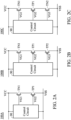
- FIG. 2C is a block diagram of a circuit protection device according to one embodiment of the present disclosure.
- a part of the circuit protection device 100C in Figure 2C may correspond to a part of the circuit protection device 100A in Figure 2A .
- the circuit protection device 100C further includes a second N-type transistor TN2.
- the second N-type transistor TN2 includes a fifth terminal, a third gate terminal, and a sixth terminal.
- the fifth terminal is connected to the fourth terminal of the first P-type transistor TP1.
- the third gate terminal is connected to the control circuit 90.
- the sixth terminal of the second N-type transistor TN2 is configured to receive the second voltage VSS.
- the second sub-terminal is configured to receive the second voltage VSS, the second sub-terminal is coupled to the sixth terminal of the second N-type transistor TN2.
- the second sub-terminal of the control circuit 90 may connect to the sixth terminal of the second P-type transistor TP2, but the present disclosure is not limited thereto.
- the first N-type transistor, the first P-type transistor, and the second N-type transistor are turned on (or turned off) in sequence, but the present disclosure is not limited thereto. In some embodiments, the first N-type transistor, the first P-type transistor, and the second N-type transistor are turned on (or turned off) at the same time, but the present disclosure is not limited thereto. In some embodiments, the second N-type transistor, the first P-type transistor, and the first N-type transistor are turned on (or turned off) in sequence, but the present disclosure is not limited thereto.
- the first N-type transistor TN1 further includes one of the NMOS transistor and the NPN BJT.
- the first P-type transistor TP1 further includes one of the PMOS transistor and the PNP BJT.
- the second N-type transistor TP2 further includes one of the NMOS transistor and the NPN BJT.
- Figure 3A is a block diagram of a circuit protection device according to one embodiment of the present disclosure.
- a part of the circuit protection device 100D in Figure 3A may correspond to a part of the circuit protection device 100B in Figure 2B .
- the circuit protection device 100D further includes a third P-type transistor TP3.
- the third P-type transistor TP3 includes a seventh terminal, a fourth gate terminal, and an eighth terminal.
- the seventh terminal is connected to the sixth terminal of the second P-type transistor TP2.
- the fourth gate terminal is connected to the control circuit 90.
- the eighth terminal of the third P-type transistor TP3 is configured to receive the second voltage VSS.
- the second sub-terminal is configured to receive the second voltage VSS, the second sub-terminal is coupled to the eighth terminal of the third P-type transistor TP3.
- the second sub-terminal of the control circuit 90 may connect to the eighth terminal of the third P-type transistor TP3, but the present disclosure is not limited thereto.
- Figure 3B is a block diagram of a circuit protection device according to one embodiment of the present disclosure. As shown in Figure 3B , in one embodiment, a part of the circuit protection device 100E in Figure 3B may correspond to a part of the circuit protection device 100B in Figure 2B . What needs special explanation is that the circuit protection device 100E further includes a second N-type transistor TN2.
- the second N-type transistor TN2 includes the seventh terminal, the fourth gate terminal, and the eighth terminal.
- the seventh terminal is connected to the sixth terminal of the second P-type transistor TP2.
- the fourth gate terminal is connected to the control circuit 90.
- the seventh terminal of the second N-type transistor TN2 may receive the signal VCC
- the fourth gate terminal of the second N-type transistor TN2 may receive the signal VG4
- the eighth terminal of the second N-type transistor TN2 may receive the signal VSS, but the present disclosure is not limited thereto.
- the eighth terminal of the second N-type transistor TN2 is configured to receive the second voltage VSS.
- the second sub-terminal is configured to receive the second voltage VSS, the second sub-terminal is coupled to the eighth terminal of the second N-type transistor TN2.
- the second sub-terminal of the control circuit 90 may connect to the eighth terminal of the second N-type transistor TN2, but the present disclosure is not limited thereto.
- Figure 3C is a block diagram of a circuit protection device according to one embodiment of the present disclosure.
- a part of the circuit protection device 100F in Figure 3C may correspond to a part of the circuit protection device 100C in Figure 2C .
- the circuit protection device 100F further includes the second P-type transistor TP2.
- the second P-type transistor includes the seventh terminal, the fourth gate terminal, and the eighth terminal.
- the seventh terminal is connected to the sixth terminal of the second N-type transistor TN2.
- the fourth gate terminal is connected to the control circuit 90.
- the seventh terminal of the second P-type transistor TP2 may receive the signal VCC
- the fourth gate terminal of the second P-type transistor TP2 may receive the signal VG4
- the eighth terminal of the second P-type transistor TP2 may receive the signal VSS, but the present disclosure is not limited thereto.
- the eighth terminal of the second P-type transistor TP2 is configured to receive the second voltage VSS.
- the second sub-terminal is configured to receive the second voltage VSS, the second sub-terminal is coupled to the eighth terminal of the second P-type transistor TP2.
- the second sub-terminal of the control circuit 90 may connect to the eighth terminal of the second P-type transistor TP2, but the present disclosure is not limited thereto.
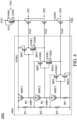
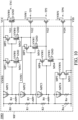
- FIG 4 is a detailed circuit diagram of a circuit protection device according to one embodiment of the present disclosure.
- a part of the circuit protection device 100G in Figure 4 may correspond to a part of the circuit protection device 100D in Figure 3A .
- the first terminal of the first N-type transistor TN1 is connected to the first gate terminal of the first N-type transistor TN1.
- the first terminal of the first N-type transistor TN1 may be not directly connected to the control circuit 90A in Figure 4
- the second terminal of the first N-type transistor TN1 may be connected to the control circuit 90A in Figure 4 , but the present disclosure is not limited thereto.
- the first terminal of the first N-type transistor TN1 may receive the first voltage VCC
- the first gate terminal of the first N-type transistor TN1 may receive the first voltage VCC
- the first terminal of the first N-type transistor TN1 may receive the voltage VCC, a first body terminal of the first N-type transistor TN1 is connected to the first terminal of the first N-type transistor TN1 and received to the voltage VNW0, a second body terminal is connected to the ground terminal, the second terminal of the first N-type transistor TN1 is connected to the control circuit 90A, and the first gate terminal is connected to the first terminal of the first N-type transistor TN1.
- the third terminal of the first P-type transistor TP1 is connected to the first N-type transistor TN1, a body terminal of the first P-type transistor TP1 is connected to the third terminal of the first P-type transistor TP1, the fourth terminal is connected to the second P-type transistor TP2, and the second gate terminal of the first P-type transistor TP1 is connected to the control circuit 90A, but the present disclosure is not limited thereto.
- the fifth terminal of the second P-type transistor TP2 is connected to the first P-type transistor TP1
- a body terminal of the second P-type transistor TP2 is connected to the first P-type transistor TP1
- the sixth terminal of the second P-type transistor TP2 is connected to the third P-type transistor TP3
- the third gate terminal of the second P-type transistor TP2 is connected to the control circuit 90A.
- a terminal of the resistor R5 is coupled to the resistor R2, and other terminal of the resistor R5 is coupled to the P-type transistor MPC2.
- a terminal of the resistor R6 is coupled to the P-type transistor MPC3, and other terminal of the resistor R6 is coupled to the N-type transistor MN3, but the present disclosure is not limited thereto.
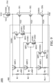
- the first terminal of the first N-type transistor TN1 may receive the voltage VCC, a first body terminal of the first N-type transistor TN1 is connected to the first terminal of the first N-type transistor TN1 and received to the voltage VNW0, a second body terminal is connected to the ground terminal, the second terminal of the first N-type transistor TN1 is connected to the first P-type transistor TP1.
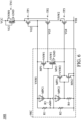
- Figure 8C is a block diagram of a circuit protection device according to one embodiment of the present disclosure. As shown in Figure 8C , in one embodiment, a part of the circuit protection device 100M in Figure 8C may correspond to a part of the circuit protection device 100E in Figure 3B . What needs special explanation is that there have a plurality of N-type transistors (such as the N-type transistors TN2 to TNN), the plurality of N-type transistors are coupled to the second P-type transistor TP2 in series.
- N-type transistors such as the N-type transistors TN2 to TNN
Landscapes
- Semiconductor Integrated Circuits (AREA)
Applications Claiming Priority (2)
| Application Number | Priority Date | Filing Date | Title |
|---|---|---|---|
| US202363614957P | 2023-12-27 | 2023-12-27 | |
| US19/001,114 US20250221054A1 (en) | 2023-12-27 | 2024-12-24 | Circuit protection device |
Publications (1)
| Publication Number | Publication Date |
|---|---|
| EP4580348A1 true EP4580348A1 (de) | 2025-07-02 |
Family
ID=94216948
Family Applications (1)
| Application Number | Title | Priority Date | Filing Date |
|---|---|---|---|
| EP24223481.3A Pending EP4580348A1 (de) | 2023-12-27 | 2024-12-27 | Schaltungsschutzvorrichtung |
Country Status (2)
| Country | Link |
|---|---|
| US (1) | US20250221054A1 (de) |
| EP (1) | EP4580348A1 (de) |
Families Citing this family (1)
| Publication number | Priority date | Publication date | Assignee | Title |
|---|---|---|---|---|
| TWI847627B (zh) * | 2023-03-24 | 2024-07-01 | 瑞昱半導體股份有限公司 | 靜電防護電路 |
Citations (4)
| Publication number | Priority date | Publication date | Assignee | Title |
|---|---|---|---|---|
| US20040135206A1 (en) * | 2003-01-15 | 2004-07-15 | Katsuhiro Kato | Semiconductor circuit having an input protection circuit |
| EP2244292A1 (de) * | 2009-04-20 | 2010-10-27 | Nxp B.V. | Integrierte Schaltung mit ESD-Schutzeinheit |
| US20130229736A1 (en) * | 2012-03-02 | 2013-09-05 | Sofics Bvba | Electrostatic discharge protection for high voltage domains |
| US20150249334A1 (en) * | 2014-02-28 | 2015-09-03 | Qualcomm Incorporated | Electrostatic discharge circuit with reduced standby current |
-
2024
- 2024-12-24 US US19/001,114 patent/US20250221054A1/en active Pending
- 2024-12-27 EP EP24223481.3A patent/EP4580348A1/de active Pending
Patent Citations (4)
| Publication number | Priority date | Publication date | Assignee | Title |
|---|---|---|---|---|
| US20040135206A1 (en) * | 2003-01-15 | 2004-07-15 | Katsuhiro Kato | Semiconductor circuit having an input protection circuit |
| EP2244292A1 (de) * | 2009-04-20 | 2010-10-27 | Nxp B.V. | Integrierte Schaltung mit ESD-Schutzeinheit |
| US20130229736A1 (en) * | 2012-03-02 | 2013-09-05 | Sofics Bvba | Electrostatic discharge protection for high voltage domains |
| US20150249334A1 (en) * | 2014-02-28 | 2015-09-03 | Qualcomm Incorporated | Electrostatic discharge circuit with reduced standby current |
Also Published As
| Publication number | Publication date |
|---|---|
| US20250221054A1 (en) | 2025-07-03 |
Similar Documents
| Publication | Publication Date | Title |
|---|---|---|
| US7268592B2 (en) | Input/output buffer for protecting a circuit from signals received from external devices | |
| US6040729A (en) | Digital output buffer for multiple voltage system | |
| EP4580348A1 (de) | Schaltungsschutzvorrichtung | |
| JP2004048354A (ja) | クランプ回路 | |
| US20110043249A1 (en) | High Voltage Tolerant Input/Output Interface Circuit | |
| US11881859B2 (en) | Schmitt trigger circuit having mismatched input and supply | |
| US20050253642A1 (en) | One way conductor | |
| US7477496B2 (en) | High input voltage tolerant input/output circuit being free from electrostatic discharge voltage | |
| US7579882B2 (en) | Output buffer circuit eliminating high voltage insulated transistor and level shift circuit, and an electronic device using the output buffer circuit | |
| US11233394B2 (en) | Electrostatic protection circuit | |
| US11296500B2 (en) | Output circuit with ESD protection | |
| US11418052B2 (en) | Power circuit and driving method thereof | |
| US6271692B1 (en) | Semiconductor integrated circuit | |
| US6661258B1 (en) | Low voltage detecting circuit for detecting input power of a modem | |
| US20200220532A1 (en) | Circuit for preventing latch-up and integrated circuit | |
| CN113422503B (zh) | 电源钳位电路及esd保护电路 | |
| US11750098B2 (en) | Voltage conversion circuit having self-adaptive mechanism | |
| CN108255753B (zh) | I/o接收机及其接收电路 | |
| KR20070095436A (ko) | 기준 전압 발생 회로 | |
| US7667491B2 (en) | Low voltage output buffer and method for buffering digital output data | |
| US20190296732A1 (en) | Circuit capable of protecting low-voltage devices | |
| US4814635A (en) | Voltage translator circuit | |
| US12268032B2 (en) | Electrostatic protection circuit and semiconductor device | |
| US12381559B2 (en) | Input/output circuit | |
| US12593512B2 (en) | Electrostatic discharge protection circuit |
Legal Events
| Date | Code | Title | Description |
|---|---|---|---|
| PUAI | Public reference made under article 153(3) epc to a published international application that has entered the european phase |
Free format text: ORIGINAL CODE: 0009012 |
|
| STAA | Information on the status of an ep patent application or granted ep patent |
Free format text: STATUS: THE APPLICATION HAS BEEN PUBLISHED |
|
| AK | Designated contracting states |
Kind code of ref document: A1 Designated state(s): AL AT BE BG CH CY CZ DE DK EE ES FI FR GB GR HR HU IE IS IT LI LT LU LV MC ME MK MT NL NO PL PT RO RS SE SI SK SM TR |
|
| STAA | Information on the status of an ep patent application or granted ep patent |
Free format text: STATUS: REQUEST FOR EXAMINATION WAS MADE |
|
| 17P | Request for examination filed |
Effective date: 20251230 |