EP4580338A1 - Vorderseitige und rückseitige source- oder drain-kontakte - Google Patents
Vorderseitige und rückseitige source- oder drain-kontakte Download PDFInfo
- Publication number
- EP4580338A1 EP4580338A1 EP24208309.5A EP24208309A EP4580338A1 EP 4580338 A1 EP4580338 A1 EP 4580338A1 EP 24208309 A EP24208309 A EP 24208309A EP 4580338 A1 EP4580338 A1 EP 4580338A1
- Authority
- EP
- European Patent Office
- Prior art keywords
- source
- drain
- dielectric material
- backside
- drain region
- Prior art date
- Legal status (The legal status is an assumption and is not a legal conclusion. Google has not performed a legal analysis and makes no representation as to the accuracy of the status listed.)
- Pending
Links
Images













Classifications
-
- H—ELECTRICITY
- H10—SEMICONDUCTOR DEVICES; ELECTRIC SOLID-STATE DEVICES NOT OTHERWISE PROVIDED FOR
- H10D—INORGANIC ELECTRIC SEMICONDUCTOR DEVICES
- H10D30/00—Field-effect transistors [FET]
- H10D30/60—Insulated-gate field-effect transistors [IGFET]
- H10D30/67—Thin-film transistors [TFT]
- H10D30/6729—Thin-film transistors [TFT] characterised by the electrodes
-
- H—ELECTRICITY
- H10—SEMICONDUCTOR DEVICES; ELECTRIC SOLID-STATE DEVICES NOT OTHERWISE PROVIDED FOR
- H10D—INORGANIC ELECTRIC SEMICONDUCTOR DEVICES
- H10D84/00—Integrated devices formed in or on semiconductor substrates that comprise only semiconducting layers, e.g. on Si wafers or on GaAs-on-Si wafers
- H10D84/01—Manufacture or treatment
- H10D84/0123—Integrating together multiple components covered by H10D12/00 or H10D30/00, e.g. integrating multiple IGBTs
- H10D84/0126—Integrating together multiple components covered by H10D12/00 or H10D30/00, e.g. integrating multiple IGBTs the components including insulated gates, e.g. IGFETs
- H10D84/0149—Manufacturing their interconnections or electrodes, e.g. source or drain electrodes
-
- H—ELECTRICITY
- H10—SEMICONDUCTOR DEVICES; ELECTRIC SOLID-STATE DEVICES NOT OTHERWISE PROVIDED FOR
- H10D—INORGANIC ELECTRIC SEMICONDUCTOR DEVICES
- H10D30/00—Field-effect transistors [FET]
- H10D30/01—Manufacture or treatment
- H10D30/019—Manufacture or treatment of FETs having stacked nanowire, nanosheet or nanoribbon channels
- H10D30/0195—Manufacture or treatment of FETs having stacked nanowire, nanosheet or nanoribbon channels forming inner spacers between adjacent channels, e.g. changing their shapes or sizes
-
- H—ELECTRICITY
- H10—SEMICONDUCTOR DEVICES; ELECTRIC SOLID-STATE DEVICES NOT OTHERWISE PROVIDED FOR
- H10D—INORGANIC ELECTRIC SEMICONDUCTOR DEVICES
- H10D30/00—Field-effect transistors [FET]
- H10D30/01—Manufacture or treatment
- H10D30/019—Manufacture or treatment of FETs having stacked nanowire, nanosheet or nanoribbon channels
- H10D30/0198—Manufacture or treatment of FETs having stacked nanowire, nanosheet or nanoribbon channels forming source or drain electrodes wherein semiconductor bodies are replaced by dielectric layers and the source or drain electrodes extend through the dielectric layers
-
- H—ELECTRICITY
- H10—SEMICONDUCTOR DEVICES; ELECTRIC SOLID-STATE DEVICES NOT OTHERWISE PROVIDED FOR
- H10D—INORGANIC ELECTRIC SEMICONDUCTOR DEVICES
- H10D30/00—Field-effect transistors [FET]
- H10D30/01—Manufacture or treatment
- H10D30/021—Manufacture or treatment of FETs having insulated gates [IGFET]
- H10D30/024—Manufacture or treatment of FETs having insulated gates [IGFET] of fin field-effect transistors [FinFET]
-
- H—ELECTRICITY
- H10—SEMICONDUCTOR DEVICES; ELECTRIC SOLID-STATE DEVICES NOT OTHERWISE PROVIDED FOR
- H10D—INORGANIC ELECTRIC SEMICONDUCTOR DEVICES
- H10D30/00—Field-effect transistors [FET]
- H10D30/40—FETs having zero-dimensional [0D], one-dimensional [1D] or two-dimensional [2D] charge carrier gas channels
- H10D30/43—FETs having zero-dimensional [0D], one-dimensional [1D] or two-dimensional [2D] charge carrier gas channels having one-dimensional [1D] charge carrier gas channels, e.g. quantum wire FETs or transistors having 1D quantum-confined channels
-
- H—ELECTRICITY
- H10—SEMICONDUCTOR DEVICES; ELECTRIC SOLID-STATE DEVICES NOT OTHERWISE PROVIDED FOR
- H10D—INORGANIC ELECTRIC SEMICONDUCTOR DEVICES
- H10D30/00—Field-effect transistors [FET]
- H10D30/40—FETs having zero-dimensional [0D], one-dimensional [1D] or two-dimensional [2D] charge carrier gas channels
- H10D30/47—FETs having zero-dimensional [0D], one-dimensional [1D] or two-dimensional [2D] charge carrier gas channels having two-dimensional [2D] charge carrier gas channels, e.g. nanoribbon FETs or high electron mobility transistors [HEMT]
-
- H—ELECTRICITY
- H10—SEMICONDUCTOR DEVICES; ELECTRIC SOLID-STATE DEVICES NOT OTHERWISE PROVIDED FOR
- H10D—INORGANIC ELECTRIC SEMICONDUCTOR DEVICES
- H10D30/00—Field-effect transistors [FET]
- H10D30/501—FETs having stacked nanowire, nanosheet or nanoribbon channels
- H10D30/507—FETs having stacked nanowire, nanosheet or nanoribbon channels characterised by inner spacers between adjacent channels
-
- H—ELECTRICITY
- H10—SEMICONDUCTOR DEVICES; ELECTRIC SOLID-STATE DEVICES NOT OTHERWISE PROVIDED FOR
- H10D—INORGANIC ELECTRIC SEMICONDUCTOR DEVICES
- H10D30/00—Field-effect transistors [FET]
- H10D30/60—Insulated-gate field-effect transistors [IGFET]
- H10D30/62—Fin field-effect transistors [FinFET]
- H10D30/6211—Fin field-effect transistors [FinFET] having fin-shaped semiconductor bodies integral with the bulk semiconductor substrates
-
- H—ELECTRICITY
- H10—SEMICONDUCTOR DEVICES; ELECTRIC SOLID-STATE DEVICES NOT OTHERWISE PROVIDED FOR
- H10D—INORGANIC ELECTRIC SEMICONDUCTOR DEVICES
- H10D30/00—Field-effect transistors [FET]
- H10D30/60—Insulated-gate field-effect transistors [IGFET]
- H10D30/62—Fin field-effect transistors [FinFET]
- H10D30/6219—Fin field-effect transistors [FinFET] characterised by the source or drain electrodes
-
- H—ELECTRICITY
- H10—SEMICONDUCTOR DEVICES; ELECTRIC SOLID-STATE DEVICES NOT OTHERWISE PROVIDED FOR
- H10D—INORGANIC ELECTRIC SEMICONDUCTOR DEVICES
- H10D30/00—Field-effect transistors [FET]
- H10D30/60—Insulated-gate field-effect transistors [IGFET]
- H10D30/67—Thin-film transistors [TFT]
- H10D30/6729—Thin-film transistors [TFT] characterised by the electrodes
- H10D30/673—Thin-film transistors [TFT] characterised by the electrodes characterised by the shapes, relative sizes or dispositions of the gate electrodes
- H10D30/6735—Thin-film transistors [TFT] characterised by the electrodes characterised by the shapes, relative sizes or dispositions of the gate electrodes having gates fully surrounding the channels, e.g. gate-all-around
-
- H—ELECTRICITY
- H10—SEMICONDUCTOR DEVICES; ELECTRIC SOLID-STATE DEVICES NOT OTHERWISE PROVIDED FOR
- H10D—INORGANIC ELECTRIC SEMICONDUCTOR DEVICES
- H10D30/00—Field-effect transistors [FET]
- H10D30/60—Insulated-gate field-effect transistors [IGFET]
- H10D30/67—Thin-film transistors [TFT]
- H10D30/6757—Thin-film transistors [TFT] characterised by the structure of the channel, e.g. transverse or longitudinal shape or doping profile
-
- H—ELECTRICITY
- H10—SEMICONDUCTOR DEVICES; ELECTRIC SOLID-STATE DEVICES NOT OTHERWISE PROVIDED FOR
- H10D—INORGANIC ELECTRIC SEMICONDUCTOR DEVICES
- H10D62/00—Semiconductor bodies, or regions thereof, of devices having potential barriers
- H10D62/10—Shapes, relative sizes or dispositions of the regions of the semiconductor bodies; Shapes of the semiconductor bodies
- H10D62/117—Shapes of semiconductor bodies
- H10D62/118—Nanostructure semiconductor bodies
- H10D62/119—Nanowire, nanosheet or nanotube semiconductor bodies
- H10D62/121—Nanowire, nanosheet or nanotube semiconductor bodies oriented parallel to substrates
-
- H—ELECTRICITY
- H10—SEMICONDUCTOR DEVICES; ELECTRIC SOLID-STATE DEVICES NOT OTHERWISE PROVIDED FOR
- H10D—INORGANIC ELECTRIC SEMICONDUCTOR DEVICES
- H10D64/00—Electrodes of devices having potential barriers
- H10D64/01—Manufacture or treatment
- H10D64/017—Manufacture or treatment using dummy gates in processes wherein at least parts of the final gates are self-aligned to the dummy gates, i.e. replacement gate processes
-
- H—ELECTRICITY
- H10—SEMICONDUCTOR DEVICES; ELECTRIC SOLID-STATE DEVICES NOT OTHERWISE PROVIDED FOR
- H10D—INORGANIC ELECTRIC SEMICONDUCTOR DEVICES
- H10D64/00—Electrodes of devices having potential barriers
- H10D64/20—Electrodes characterised by their shapes, relative sizes or dispositions
- H10D64/23—Electrodes carrying the current to be rectified, amplified, oscillated or switched, e.g. sources, drains, anodes or cathodes
- H10D64/251—Source or drain electrodes for field-effect devices
-
- H—ELECTRICITY
- H10—SEMICONDUCTOR DEVICES; ELECTRIC SOLID-STATE DEVICES NOT OTHERWISE PROVIDED FOR
- H10D—INORGANIC ELECTRIC SEMICONDUCTOR DEVICES
- H10D84/00—Integrated devices formed in or on semiconductor substrates that comprise only semiconducting layers, e.g. on Si wafers or on GaAs-on-Si wafers
- H10D84/01—Manufacture or treatment
- H10D84/0123—Integrating together multiple components covered by H10D12/00 or H10D30/00, e.g. integrating multiple IGBTs
- H10D84/0126—Integrating together multiple components covered by H10D12/00 or H10D30/00, e.g. integrating multiple IGBTs the components including insulated gates, e.g. IGFETs
- H10D84/0151—Manufacturing their isolation regions
-
- H—ELECTRICITY
- H10—SEMICONDUCTOR DEVICES; ELECTRIC SOLID-STATE DEVICES NOT OTHERWISE PROVIDED FOR
- H10D—INORGANIC ELECTRIC SEMICONDUCTOR DEVICES
- H10D84/00—Integrated devices formed in or on semiconductor substrates that comprise only semiconducting layers, e.g. on Si wafers or on GaAs-on-Si wafers
- H10D84/01—Manufacture or treatment
- H10D84/0123—Integrating together multiple components covered by H10D12/00 or H10D30/00, e.g. integrating multiple IGBTs
- H10D84/0126—Integrating together multiple components covered by H10D12/00 or H10D30/00, e.g. integrating multiple IGBTs the components including insulated gates, e.g. IGFETs
- H10D84/0165—Integrating together multiple components covered by H10D12/00 or H10D30/00, e.g. integrating multiple IGBTs the components including insulated gates, e.g. IGFETs the components including complementary IGFETs, e.g. CMOS devices
- H10D84/017—Manufacturing their source or drain regions, e.g. silicided source or drain regions
-
- H—ELECTRICITY
- H10—SEMICONDUCTOR DEVICES; ELECTRIC SOLID-STATE DEVICES NOT OTHERWISE PROVIDED FOR
- H10D—INORGANIC ELECTRIC SEMICONDUCTOR DEVICES
- H10D84/00—Integrated devices formed in or on semiconductor substrates that comprise only semiconducting layers, e.g. on Si wafers or on GaAs-on-Si wafers
- H10D84/01—Manufacture or treatment
- H10D84/0123—Integrating together multiple components covered by H10D12/00 or H10D30/00, e.g. integrating multiple IGBTs
- H10D84/0126—Integrating together multiple components covered by H10D12/00 or H10D30/00, e.g. integrating multiple IGBTs the components including insulated gates, e.g. IGFETs
- H10D84/0165—Integrating together multiple components covered by H10D12/00 or H10D30/00, e.g. integrating multiple IGBTs the components including insulated gates, e.g. IGFETs the components including complementary IGFETs, e.g. CMOS devices
- H10D84/0186—Manufacturing their interconnections or electrodes, e.g. source or drain electrodes
-
- H—ELECTRICITY
- H10—SEMICONDUCTOR DEVICES; ELECTRIC SOLID-STATE DEVICES NOT OTHERWISE PROVIDED FOR
- H10D—INORGANIC ELECTRIC SEMICONDUCTOR DEVICES
- H10D84/00—Integrated devices formed in or on semiconductor substrates that comprise only semiconducting layers, e.g. on Si wafers or on GaAs-on-Si wafers
- H10D84/01—Manufacture or treatment
- H10D84/0123—Integrating together multiple components covered by H10D12/00 or H10D30/00, e.g. integrating multiple IGBTs
- H10D84/0126—Integrating together multiple components covered by H10D12/00 or H10D30/00, e.g. integrating multiple IGBTs the components including insulated gates, e.g. IGFETs
- H10D84/0165—Integrating together multiple components covered by H10D12/00 or H10D30/00, e.g. integrating multiple IGBTs the components including insulated gates, e.g. IGFETs the components including complementary IGFETs, e.g. CMOS devices
- H10D84/0193—Integrating together multiple components covered by H10D12/00 or H10D30/00, e.g. integrating multiple IGBTs the components including insulated gates, e.g. IGFETs the components including complementary IGFETs, e.g. CMOS devices the components including FinFETs
-
- H—ELECTRICITY
- H10—SEMICONDUCTOR DEVICES; ELECTRIC SOLID-STATE DEVICES NOT OTHERWISE PROVIDED FOR
- H10D—INORGANIC ELECTRIC SEMICONDUCTOR DEVICES
- H10D84/00—Integrated devices formed in or on semiconductor substrates that comprise only semiconducting layers, e.g. on Si wafers or on GaAs-on-Si wafers
- H10D84/01—Manufacture or treatment
- H10D84/02—Manufacture or treatment characterised by using material-based technologies
- H10D84/03—Manufacture or treatment characterised by using material-based technologies using Group IV technology, e.g. silicon technology or silicon-carbide [SiC] technology
- H10D84/038—Manufacture or treatment characterised by using material-based technologies using Group IV technology, e.g. silicon technology or silicon-carbide [SiC] technology using silicon technology, e.g. SiGe
-
- H—ELECTRICITY
- H10—SEMICONDUCTOR DEVICES; ELECTRIC SOLID-STATE DEVICES NOT OTHERWISE PROVIDED FOR
- H10D—INORGANIC ELECTRIC SEMICONDUCTOR DEVICES
- H10D84/00—Integrated devices formed in or on semiconductor substrates that comprise only semiconducting layers, e.g. on Si wafers or on GaAs-on-Si wafers
- H10D84/80—Integrated devices formed in or on semiconductor substrates that comprise only semiconducting layers, e.g. on Si wafers or on GaAs-on-Si wafers characterised by the integration of at least one component covered by groups H10D12/00 or H10D30/00, e.g. integration of IGFETs
- H10D84/82—Integrated devices formed in or on semiconductor substrates that comprise only semiconducting layers, e.g. on Si wafers or on GaAs-on-Si wafers characterised by the integration of at least one component covered by groups H10D12/00 or H10D30/00, e.g. integration of IGFETs of only field-effect components
- H10D84/83—Integrated devices formed in or on semiconductor substrates that comprise only semiconducting layers, e.g. on Si wafers or on GaAs-on-Si wafers characterised by the integration of at least one component covered by groups H10D12/00 or H10D30/00, e.g. integration of IGFETs of only field-effect components of only insulated-gate FETs [IGFET]
- H10D84/832—Integrated devices formed in or on semiconductor substrates that comprise only semiconducting layers, e.g. on Si wafers or on GaAs-on-Si wafers characterised by the integration of at least one component covered by groups H10D12/00 or H10D30/00, e.g. integration of IGFETs of only field-effect components of only insulated-gate FETs [IGFET] comprising IGFETs having stacked nanowire, nanosheet or nanoribbon channels
-
- H—ELECTRICITY
- H10—SEMICONDUCTOR DEVICES; ELECTRIC SOLID-STATE DEVICES NOT OTHERWISE PROVIDED FOR
- H10D—INORGANIC ELECTRIC SEMICONDUCTOR DEVICES
- H10D84/00—Integrated devices formed in or on semiconductor substrates that comprise only semiconducting layers, e.g. on Si wafers or on GaAs-on-Si wafers
- H10D84/80—Integrated devices formed in or on semiconductor substrates that comprise only semiconducting layers, e.g. on Si wafers or on GaAs-on-Si wafers characterised by the integration of at least one component covered by groups H10D12/00 or H10D30/00, e.g. integration of IGFETs
- H10D84/82—Integrated devices formed in or on semiconductor substrates that comprise only semiconducting layers, e.g. on Si wafers or on GaAs-on-Si wafers characterised by the integration of at least one component covered by groups H10D12/00 or H10D30/00, e.g. integration of IGFETs of only field-effect components
- H10D84/83—Integrated devices formed in or on semiconductor substrates that comprise only semiconducting layers, e.g. on Si wafers or on GaAs-on-Si wafers characterised by the integration of at least one component covered by groups H10D12/00 or H10D30/00, e.g. integration of IGFETs of only field-effect components of only insulated-gate FETs [IGFET]
- H10D84/85—Complementary IGFETs, e.g. CMOS
- H10D84/853—Complementary IGFETs, e.g. CMOS comprising FinFETs
-
- H—ELECTRICITY
- H10—SEMICONDUCTOR DEVICES; ELECTRIC SOLID-STATE DEVICES NOT OTHERWISE PROVIDED FOR
- H10W—GENERIC PACKAGES, INTERCONNECTIONS, CONNECTORS OR OTHER CONSTRUCTIONAL DETAILS OF DEVICES COVERED BY CLASS H10
- H10W20/00—Interconnections in chips, wafers or substrates
- H10W20/01—Manufacture or treatment
- H10W20/031—Manufacture or treatment of conductive parts of the interconnections
- H10W20/069—Manufacture or treatment of conductive parts of the interconnections by forming self-aligned vias or self-aligned contact plugs
-
- H—ELECTRICITY
- H10—SEMICONDUCTOR DEVICES; ELECTRIC SOLID-STATE DEVICES NOT OTHERWISE PROVIDED FOR
- H10W—GENERIC PACKAGES, INTERCONNECTIONS, CONNECTORS OR OTHER CONSTRUCTIONAL DETAILS OF DEVICES COVERED BY CLASS H10
- H10W20/00—Interconnections in chips, wafers or substrates
- H10W20/40—Interconnections external to wafers or substrates, e.g. back-end-of-line [BEOL] metallisations or vias connecting to gate electrodes
- H10W20/41—Interconnections external to wafers or substrates, e.g. back-end-of-line [BEOL] metallisations or vias connecting to gate electrodes characterised by their conductive parts
- H10W20/427—Power or ground buses
-
- H—ELECTRICITY
- H10—SEMICONDUCTOR DEVICES; ELECTRIC SOLID-STATE DEVICES NOT OTHERWISE PROVIDED FOR
- H10W—GENERIC PACKAGES, INTERCONNECTIONS, CONNECTORS OR OTHER CONSTRUCTIONAL DETAILS OF DEVICES COVERED BY CLASS H10
- H10W20/00—Interconnections in chips, wafers or substrates
- H10W20/40—Interconnections external to wafers or substrates, e.g. back-end-of-line [BEOL] metallisations or vias connecting to gate electrodes
- H10W20/41—Interconnections external to wafers or substrates, e.g. back-end-of-line [BEOL] metallisations or vias connecting to gate electrodes characterised by their conductive parts
- H10W20/435—Cross-sectional shapes or dispositions of interconnections
-
- H—ELECTRICITY
- H10—SEMICONDUCTOR DEVICES; ELECTRIC SOLID-STATE DEVICES NOT OTHERWISE PROVIDED FOR
- H10W—GENERIC PACKAGES, INTERCONNECTIONS, CONNECTORS OR OTHER CONSTRUCTIONAL DETAILS OF DEVICES COVERED BY CLASS H10
- H10W20/00—Interconnections in chips, wafers or substrates
- H10W20/40—Interconnections external to wafers or substrates, e.g. back-end-of-line [BEOL] metallisations or vias connecting to gate electrodes
- H10W20/481—Interconnections external to wafers or substrates, e.g. back-end-of-line [BEOL] metallisations or vias connecting to gate electrodes on the rear surfaces of the wafers or substrates
-
- B—PERFORMING OPERATIONS; TRANSPORTING
- B82—NANOTECHNOLOGY
- B82Y—SPECIFIC USES OR APPLICATIONS OF NANOSTRUCTURES; MEASUREMENT OR ANALYSIS OF NANOSTRUCTURES; MANUFACTURE OR TREATMENT OF NANOSTRUCTURES
- B82Y10/00—Nanotechnology for information processing, storage or transmission, e.g. quantum computing or single electron logic
-
- H—ELECTRICITY
- H10—SEMICONDUCTOR DEVICES; ELECTRIC SOLID-STATE DEVICES NOT OTHERWISE PROVIDED FOR
- H10D—INORGANIC ELECTRIC SEMICONDUCTOR DEVICES
- H10D30/00—Field-effect transistors [FET]
- H10D30/60—Insulated-gate field-effect transistors [IGFET]
- H10D30/791—Arrangements for exerting mechanical stress on the crystal lattice of the channel regions
- H10D30/797—Arrangements for exerting mechanical stress on the crystal lattice of the channel regions being in source or drain regions, e.g. SiGe source or drain
-
- H—ELECTRICITY
- H10—SEMICONDUCTOR DEVICES; ELECTRIC SOLID-STATE DEVICES NOT OTHERWISE PROVIDED FOR
- H10D—INORGANIC ELECTRIC SEMICONDUCTOR DEVICES
- H10D62/00—Semiconductor bodies, or regions thereof, of devices having potential barriers
- H10D62/10—Shapes, relative sizes or dispositions of the regions of the semiconductor bodies; Shapes of the semiconductor bodies
- H10D62/113—Isolations within a component, i.e. internal isolations
- H10D62/115—Dielectric isolations, e.g. air gaps
- H10D62/116—Dielectric isolations, e.g. air gaps adjoining the input or output regions of field-effect devices, e.g. adjoining source or drain regions
-
- H—ELECTRICITY
- H10—SEMICONDUCTOR DEVICES; ELECTRIC SOLID-STATE DEVICES NOT OTHERWISE PROVIDED FOR
- H10D—INORGANIC ELECTRIC SEMICONDUCTOR DEVICES
- H10D62/00—Semiconductor bodies, or regions thereof, of devices having potential barriers
- H10D62/80—Semiconductor bodies, or regions thereof, of devices having potential barriers characterised by the materials
- H10D62/82—Heterojunctions
- H10D62/822—Heterojunctions comprising only Group IV materials heterojunctions, e.g. Si/Ge heterojunctions
Definitions
- a field-effect transistor is a semiconductor device that includes three terminals: a gate, a source, and a drain.
- a FET uses an electric field applied by the gate to control the electrical conductivity of a channel through which charge carriers (e.g., electrons or holes) flow between the source and drain.
- charge carriers e.g., electrons or holes
- the FET is referred to as an n-channel device; and in instances where the charge carriers are holes, the FET is referred to as a p-channel device.
- MOSFETs metal-oxide-semiconductor FETs
- MOSFETs include a gate dielectric between the gate and the channel.
- MOSFETs may also be known as metal-insulator-semiconductor FETs (MISFETSs) or insulated-gate FETs (IGFETs).
- MISFETSs metal-insulator-semiconductor FETs
- IGFETs insulated-gate FETs
- Complementary MOS (CMOS) structures use a combination of p-channel MOSFET (PMOS) and n-channel MOSFET (NMOS) devices to implement logic gates and other digital circuits.
- PMOS p-channel MOSFET
- NMOS n-channel MOSFET
- a FinFET is a MOSFET transistor built around a thin strip of semiconductor material (generally referred to as a fin).
- the conductive channel of the FinFET device resides on the outer portions of the fin adjacent to the gate dielectric. Specifically, current runs along/within both sidewalls of the fin (sides perpendicular to the substrate surface) as well as along the top of the fin (side parallel to the substrate surface). Because the conductive channel of such configurations includes three different planer regions of the fin (e.g., top and two sides), such a FinFET design is sometimes referred to as a tri-gate transistor.
- a gate-all-around (GAA) transistor is configured similarly to a fin-based transistor, but instead of a finned channel region, one or more channel bodies such as nanoribbons or nanowires extend between the source and the drain regions. In GAA transistors, the gate material wraps around each such body.
- Scaling of integrated circuit structures results in high density of scaled interconnect features.
- One approach to circumvent congestion of frontside interconnects due to power and signal routing includes the use of a backside power and/or signal delivery.
- backside power and/or signal delivery includes the use of a backside power and/or signal delivery.
- Microelectronic device structures including both frontside source or drain contacts, and backside source or drain contacts, and techniques for forming such frontside and backside source or drain contacts, are provided herein.
- the techniques are particularly useful in gate-all-around (GAA) transistor architectures such as nanowire and nanoribbon transistors, although they may also benefit other transistor topologies such as forksheet transistors or other transistors having epitaxial source and drain regions.
- GAA gate-all-around
- trenches for backside source or drain contacts are formed from the frontside during source and drain processing, and sacrificial dielectric material is deposited within the trenches (e.g., within lower portions of the trenches, such as portions of the trenches extending within the sub-fin regions) from the frontside, e.g., during gate spacer deposition process.
- the sacrificial dielectric material and the gate spacer material comprise the same elemental constituents, and are elementally (and may also be compositionally) the same, as the sacrificial dielectric material is deposited during the gate spacer formation process.
- epitaxial (epi) source or drain regions are formed within the trenches and above the sacrificial dielectric material.
- epi epitaxial
- the sacrificial material coupled to the given source or drain region is removed from the backside, and replaced with conductive material.
- the sacrificial material coupled to the backside of the second source or drain region is left in place.
- a given source or drain region may have a source or drain contact at its backside, or has dielectric material at its backside, where the dielectric material is elementally (and also may be compositionally) the same as the gate spacer material.
- the dielectric material and the gate spacer material comprise the same elemental constituents. Numerous configurations and variations will be apparent in light of this disclosure.
- the sacrificial material coupled to the first source or drain region is removed from the backside, and replaced with conductive material.
- the first source or drain contact is, thus, self-aligned to the first source or drain region.
- the trench for the first source or drain contact is formed from the frontside, and the sacrificial dielectric material is also deposited from the frontside during the gate spacer deposition process, without causing any damage, or reduced damage, to surrounding material, thereby improving yield and performance.
- At least portions of the dielectric material occupying the lower portions of at least some of the trenches are later removed and replaced with conductive material to form backside source or drain contacts, and hence, the dielectric material occupying the lower portions of the trenches is referred as sacrificial dielectric material. Note, however, that in some instances, the sacrificial dielectric material may be left intact within the final integrated circuit structure.
- each source or drain region is self-aligned with the corresponding sacrificial dielectric material at the bottom of the source or drain trench and below the source or drain region.
- one or more source or drain regions have frontside source or drain contacts coupled to the frontside interconnect structure.
- the frontside of the wafer is bonded to a carrier wafer, so as to allow for access to the backside of the wafer.
- the substrate is removed, and at least a portion of the sub-fin regions are removed and replaced with dielectric material.
- the sacrificial dielectric material within the trenches is exposed from the backside.
- the sacrificial dielectric material is not exposed from the backside, and is still covered by a dielectric material used to replace the sub-fin regions.
- a mask is patterned on the backside, where the mask has one or more openings above corresponding the sacrificial dielectric material, which is to be replaced with conductive materials, to form corresponding backside source or drain contacts.
- the mask may cover one or more other locations of the sacrificial material, with those location being coupled to source or drain regions having frontside source or drain contacts. For example, assume that the mask has an opening above a first sacrificial material coupled to a first source or drain region, and doesn't have an opening above a second sacrificial material coupled to a second source or drain region (where the second source or drain region may have a frontside source or drain contact).
- the first sacrificial material is removed from the backside through the opening within the mask, and subsequently replaced with a conductive material, to form a backside source or drain contact for the first source or drain region.
- the second sacrificial material coupled to the second source or drain region is not removed, because it is covered by the mask.
- the backside surfaces of the backside source or drain contact for the first source or drain region and the second sacrificial material are substantially coplanar, such as within a tolerance of at most 5 nm, or at most 3 nm, or at most 2 nm, or at most 1 nm, for example, as will be described below.
- Some variances in trench depth may occur, due to factors such as the trench geometries and loading (similarly shaped and spaced trenches will tend to etch similarly, whereas differently shaped and spaced trenches may etch at different rates and thus have more divergent trench depths).
- the opening within the mask doesn't reveal the first sacrificial material (e.g., for being covered by the dielectric material that is used to replace the sub-fin regions).
- the first sacrificial material replacement is performed using two removal processes through the opening within the mask: (i) a first removal process that removes the dielectric material covering the first sacrificial material, and (ii) a second removal process that removes the first sacrificial material.
- group IV semiconductor material includes at least one group IV element (e.g., silicon, germanium, carbon, tin), such as silicon (Si), germanium (Ge), silicon-germanium (SiGe), and so forth.
- group IV element e.g., silicon, germanium, carbon, tin
- Si silicon
- germanium Ge
- SiGe silicon-germanium
- group III-V semiconductor material includes at least one group III element (e.g., aluminum, gallium, indium) and at least one group V element (e.g., nitrogen, phosphorus, arsenic, antimony, bismuth), such as gallium arsenide (GaAs), indium gallium arsenide (InGaAs), indium aluminum arsenide (InAIAs), gallium phosphide (GaP), gallium antimonide (GaSb), indium phosphide (InP), gallium nitride (GaN), and so forth.
- group III may also be known as the boron group or IUPAC group 13
- group IV may also be known as the carbon group or IUPAC group 14
- group V may also be known as the nitrogen family or IUPAC group 15, for example.
- compositionally different refers to two materials that have different chemical compositions. This compositional difference may be, for instance, by virtue of an element that is in one material but not the other (e.g., SiGe is compositionally different than silicon), or by way of one material having all the same elements as a second material but at least one of those elements is intentionally provided at a different concentration in one material relative to the other material (e.g., SiGe having 70 atomic percent germanium is compositionally different than from SiGe having 25 atomic percent germanium).
- the materials may also have distinct dopants (e.g., gallium and magnesium) or the same dopants but at differing concentrations.
- compositionally distinct materials may further refer to two materials that have different crystallographic orientations. For instance, (110) silicon is compositionally distinct or different from (100) silicon. Creating a stack of different orientations could be accomplished, for instance, with blanket wafer layer transfer. If two materials are elementally different, then one of the material has an element that is not in the other material. If two materials are elementally the same, then the two materials comprise the same elemental constituents.
- TEM/TEM scanning/transmission electron microscopy
- TEM-EELS TEM electron energy loss spectroscopy
- STEM-EELS scanning transmission electron microscopy
- STEM nano-beam electron diffraction
- REM reflection electron microscopy
- composition mapping x-ray crystallography or diffraction
- EDX energy-dispersive x-ray spectroscopy
- SIMS secondary ion mass spectrometry
- TOF-SIMS time-of-flight SIMS
- atom probe imaging or tomography APT
- LAP local electrode atom probe
- such tools may be used to detect an integrated circuit structure including a device layer having some source and/or drain regions contacted with frontside contacts, and some source or drain regions contacted by backside contacts, wherein source/drain recesses extend into the subfin region even in non-backside contact regions where the recesses have their bottoms filled with dielectric material that is also used for the internal gate spacers.
- a given backside contact has its critical expanded, TEM-EELS, APT or SIMs may show etchant species next to the backside contact. Numerous configurations and variations will be apparent in light of this disclosure.
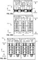
- FIGs. 1A, 1B , 1C, and 1D illustrate various views of an integrated circuit structure 100 (also referred to herein as "structure 100") comprising a device layer 150 including a plurality of integrated circuit devices (such as GAA devices), each device including (i) one or more source or drain regions 126, (ii) a channel region including one or more bodies 103 comprising semiconductor material extending laterally between two corresponding source or drain regions, (iii) a gate stack comprising a gate electrode 112 wrapped at least in part around the one or more bodies, and (iv) a gate spacer 110 laterally between and separating a corresponding a source or drain region 126 and a corresponding gate electrode 112, wherein the gate spacer 110 comprises a first dielectric material, wherein a first source or drain contact 125b is coupled to a frontside of a first source or drain region 126b of the device layer 104, wherein a layer 114b comprising a second dielectric material is coupled to a backside of the first source
- the cross-section view of Fig. 1A is taken parallel to, and through, the source or drain regions.
- the cross-section view of Fig. 1A is a channel-cut view centered on the source or drain regions, and accordingly, the gate stack is not illustrated in Fig. 1A .
- the cross-section view of Fig. 1B is taken parallel to, and through, the gate stack.
- the cross-section view of Fig. 1B is a channel-cut view centered on the gate stack. Accordingly, the source or drain regions are not illustrated in Fig. 1B .
- the cross-section view of Fig. 1C is taken parallel to, and through, the fin structure (e.g., by cutting through the gate stack), such that the channel, source, and drain regions are shown.
- the cross-section view of Fig. 1C is a gate-cut view centered on the channel regions.
- the cross-section view of Fig. 1A is along line A-A' of Fig. 1C .
- the cross-section view of Fig. 1B is along line B-B' of Fig. 1C .
- Fig. 1D is a plan view of the structure 100, when viewed from the backside of the structure 100, e.g., along lines D-D' of Figs. 1B and 1C .
- the devices within the device layer 150 are arranged in an array including a plurality of laterally adjacent devices. Accordingly, the devices, including the source or drain regions of the devices illustrated in Fig. 1A does not necessarily match with the devices, including the source or drain regions of the devices illustrated in Figs. 1B and/or 1C. Note that Figs. 1A and 1B are along the X-Z plane, while Fig. 1C is along the Y-Z plane.
- the structure 100 includes the device layer 150 comprising a plurality of devices, such as GAA devices.
- a section of the structure 100 above the device layer 150 is referred to as a frontside of the device layer 150
- another section of the structure 100 below the device layer 150 is referred to herein as a backside of the of the device layer 150.
- the frontside and backside are symbolically illustrated in Figs. 1A-1C using respective arrows. In an example, the frontside and the backside are respectively the front and backsides of individual transistor devices within the device layer 150.
- the structure 100 comprises a frontside interconnect structure 101 on the frontside (or above, in the orientations of Figs. 1A-1C ) of the device layer 150.
- the structure 100 comprises a backside interconnect structure 102 on the backside (or below, in the orientations of Figs. 1A-1C ) of the device layer 150.
- the frontside interconnect structure 101 comprises various back end of line (BEOL) metallization layers, such as a plurality of conductive interconnect features 124 within one or more layers 122 of dielectric material.
- BEOL back end of line
- Various such layers 122 of dielectric material may be separated by corresponding etch stop layers, although the etch stop layers are not illustrated in Figs. 1A-1C .
- the conductive interconnect features 124 may be conductive lines and/or conductive vias, in an example.
- the backside interconnect structure 102 comprises various backside metallization layers, such as a plurality of conductive interconnect features 144 within one or more layers 142 of dielectric material.
- Various such layers 142 of dielectric material may be separated by corresponding etch stop layers, although the etch stop layers are not illustrated in Figs. 1A-1C .
- the conductive interconnect features 144 may be conductive lines and/or conductive vias, in an example.
- one or more of the devices included in the device layer 150 of the structure 100 each includes a corresponding channel layer comprising one or more bodies 103, where the one or more bodies comprise semiconductor material.
- the semiconductor bodies 103 included in the channel regions of the devices can vary in form, and in some examples described herein are in the form of nanoribbons.
- the channel region of each depicted devices in this example case includes a vertical stack of four nanoribbons 103 (see Figs. 1B and 1C ).
- Other examples may include fewer nanoribbons per channel region (e.g., one, two, or three), or more nanoribbons per channel region (e.g., five or six).
- Still other embodiments may include other channel configurations, such as one or more nanowires or nanosheets or other semiconductor bodies.
- the present disclosure is not intended to be limited to any particular channel configuration or topology; rather the techniques provided herein can be used in any transistor architecture that uses complementary type of adjacent transistors.
- the devices of the device layer 150 may also include stacked transistor devices, where, for example, an NMOS transistor device is stacked atop a PMOS transistor device, and this stacking is repeated laterally, to form a plurality of laterally adjacent stacked device pairs.
- Each device includes one or more source or drain regions 126.
- the four illustrated source or drain regions are specifically labelled as 126a, 126b, 126c, 126d.
- the source or drain regions illustrated in Fig. 1A are generally labelled as source or drain regions 126.
- a source or drain region may be configured as a source region, or as a drain region. Note that in an example, the location of a source region and a drain region in a device may be interchanged, and hence, these regions are generally referred to as source or drain regions.
- Each device may include a corresponding source region and a drain region. In the devices of the device layer 150 of the structure 100, each of the source or drain regions 126 is adj acent to a gated channel region on either side. Other embodiments may not have gated channel regions to each side of a source or drain region.
- the source and drain regions 126 can be any suitable semiconductor material and may include any dopant scheme.
- source or drain regions of a PMOS device can be PMOS source or drain regions that include, for example, group IV semiconductor materials such as silicon, germanium, SiGe, germanium tin (GeSn), SiGe alloyed with carbon (SiGe:C).
- group IV semiconductor materials such as silicon, germanium, SiGe, germanium tin (GeSn), SiGe alloyed with carbon (SiGe:C).
- Example p-type dopants include boron, gallium, indium, and aluminum.
- source or drain regions of a NMOS device can be NMOS source and drain regions that include, for example, silicon or group III-V semiconductor materials such as two or more of indium, aluminum, arsenic, phosphorus, gallium, and antimony, with some example compounds including but not limited to indium aluminum arsenide, indium arsenide phosphide, indium gallium arsenide, indium gallium arsenide phosphide, gallium antimonide, gallium aluminum antimonide, indium gallium antimonide, or indium gallium phosphide antimonide.
- silicon or group III-V semiconductor materials such as two or more of indium, aluminum, arsenic, phosphorus, gallium, and antimony, with some example compounds including but not limited to indium aluminum arsenide, indium arsenide phosphide, indium gallium arsenide, indium gallium arsenide phosphide, gallium antimonide, gallium aluminum antimonide, indium gallium
- PMOS source and drain regions are boron-doped SiGe, and NMOS source and drain regions are phosphorus-doped silicon.
- the source and drain regions can be any semiconductor material suitable for a given application.
- individual portions of an epitaxially formed source or drain region may include a multilayer structure, such as a germanium cap on a SiGe body, or a germanium body and a carbon-containing SiGe spacer or liner between the corresponding channel region and that germanium body.
- a portion of the epi source and drain regions may have a component that is graded in concentration, such as a graded germanium concentration to facilitate lattice matching, or a graded dopant concentration to facilitate low contact resistance.
- Any number of source and drain configurations can be used as will be appreciated, and the present disclosure is not intended to be limited to any particular such configurations.
- Adjacent source or drain regions 126 are separated from each other by a layer 120 comprising dielectric material, such as an interlayer dielectric material (ILD), as illustrated in Fig. 1A .
- the layer 120 is also between adjacent gate stacks comprising gate electrodes 112 of adjacent devices, as illustrated in Fig. 1B .
- the dielectric material of the layer 120 may comprise an appropriate nitride, oxide, carbide, oxycarbide, oxynitride, and/or oxycarbonitride, and/or may (or may not) include silicon, for example, although any other appropriate dielectric material may also be used.
- Each source or drain region 126 has a corresponding source or drain contact (although in one example, a source or drain region may not have a corresponding source or drain contact, such as an example case where the source or drain region is not contacted).
- a source or drain contact for a given source or drain region may be from a frontside of the source or drain region 126 or a backside of the source or drain region, which are respectively referred to as a frontside source or drain contact, or a backside source or drain contact.
- the structure 100 may have backside power and/or signal routing (such as backside power routing) using backside interconnect structure 102, as well as frontside power and/or signal routing (such as frontside signal routing) using frontside interconnect structure 101.
- power to one or more devices of the device layer 150 may be delivered using backside source or drain contacts, and signals may be routed using frontside source or drain contacts.
- one or more source regions may have corresponding backside source contacts for receiving power (as source region of a device may receive power), whereas one or more drain regions may have corresponding frontside drain contacts for routing signals, although the location of a source region and a drain region and positions of source or drain contacts thereof in a device may be interchanged.
- Fig. 1A illustrates three example source or drain regions 126, where two right source or drain regions have source or drain contacts 125 from a frontside of the source or drain regions (e.g., have frontside source or drain contacts), and a left source or drain region has a source or drain contact 140 from a backside of the source or drain region (e.g., has a backside source or drain contact).
- Fig. 1C illustrates four source or drain regions 126a, 126b, 126c, 126d.
- the source or drain regions 126a and 126d have backside source or drain contacts 140a and 140d, respectively.
- the source or drain regions 126b and 126c have frontside source or drain contacts 125b and 125c, respectively.
- two adjacent source or drain regions 126a and 126b of a device of the device layer 150 have respectively a backside source or drain contact 140a and a frontside source or drain contact 125b, as illustrated in Fig. 1C .
- the frontside of the source or drain regions 126a and 126d do not have any corresponding source or drain contacts. Accordingly, the frontside of the source or drain regions 126a and 126d are also covered with the above described layer 120 of dielectric material, as illustrated in Fig. 1C .
- the source or drain regions 126 that have frontside source or drain contacts have a dielectric material 114 on its backside, as illustrated in Figs. 1A and 1C .
- the source or drain region 126b is coupled to, such as in contact with, dielectric material 114b
- the source or drain region 126c is coupled to, such as in contact with, dielectric material 114c, as illustrated in Fig. 1C .
- lower surfaces of the backside source or drain contacts 140 and lower surfaces of the dielectric materials 114 are substantially coplanar, such as within a tolerance of at most 8 nm, or at most 5 nm, or at most 3 nm, or at most 2 nm, or at most 1 nm, for example.
- the lower surfaces of the backside source or drain contacts 140a, 140d and lower surfaces of the dielectric materials 114b, 114c are substantially coplanar, as illustrated in Fig. 1C . Note that in the orientation illustrated in Figs. 1A-1C , "lower” implies towards the backside, and "upper” implies towards the frontside.
- trenches for the backside source or drain contacts 140a, 140d and the dielectric materials 114b, 114c are all formed from the frontside. Accordingly, each of the backside contacts 140a, 140d and the dielectric materials 114b, 114c are tapered. Accordingly, for each of these, a width of an upper surface is higher a width of the lower surface, e.g., by at least 10%, or at least 8%, or at least 5%, or at least 3%, or at least 2%, where the upper surface is towards the frontside and the lower surface is towards the backside.
- Fig. 1C illustrates the source or drain contacts 140a, 140d and the dielectric materials 114b, 114c tapered in the manner described above.
- the taper angle of one or more of these trenches can be changed during back-side processing, e.g., to make the backside surface wider than the frontside surface.
- some of the dielectric materials 114 are removed and replaced with the conductive material to form the source or drain contacts 140a, 140b.
- an etch can blow out the corners of material 106 at the locations of the trenches for the source or drain contacts 140a and 140d.
- one or more of the backside source or drain contacts 140a, 140d may not taper in the manner described above.
- each of the devices of the device layer 150 comprises gate spacers 110 that separates a corresponding source or drain region 126 from a corresponding gate electrode 112.
- the dielectric materials 114 and the gate spacers 110 are deposited using the same deposition process.
- the dielectric materials 114 and the gate spacers 110 are elementally and/or compositionally same.
- the dielectric materials 114 and the gate spacers 110 comprise the same elemental constituents.
- the dielectric materials 114 and the gate spacers 110 comprise a nitride, oxide, carbide, oxycarbide, oxynitride, and/or oxycarbonitride, such as silicon nitride (Si3N4), silicon oxycarbonitride (SiOCN), or another dielectric material used as gate spacers.
- a nitride, oxide, carbide, oxycarbide, oxynitride, and/or oxycarbonitride such as silicon nitride (Si3N4), silicon oxycarbonitride (SiOCN), or another dielectric material used as gate spacers.
- a conductive lining layer may be between a source or drain region 126 and a corresponding source or drain contact 125 or 140.
- the conductive lining layer may include one or more of silicide layer(s), germanide layer(s), germanosilicide layer(s), and/or adhesive layer(s) between the conductive source or drain metal contact and the adjacent source or drain region.
- the source or drain contacts 125, 140 comprise a conductive fill material, such as one or more of molybdenum (Mo), tungsten (W), cobalt (Co), titanium (Ti), vanadium (V), zirconium (Zr), Niobium (Nb), nickel (Ni), ruthenium (Ru), tantalum (Ta), titanium nitride (TiN), and/or vanadium nitride (VN), for example.
- Mo molybdenum
- W tungsten
- Co cobalt
- Ti titanium
- V zirconium
- Ru nickel
- TiN titanium nitride
- VN vanadium nitride
- a gate structure wraps around each of the corresponding nanoribbons 103 in the corresponding channel region.
- the gate structures are visible in Figs. 1B and 1C .
- Each of the gate structures comprises a corresponding gate electrode 112 and corresponding dielectric material 128.
- the gate dielectric material 128 is illustrated in a magnified view of a section 115 of a device of the layer 150 in Fig. 1C .
- the gate dielectric material 128 warps around middle section of individual nanoribbons 103, and end sections of individual nanoribbons 103 are wrapped around by the gate spacers 110.
- the gate dielectric material 128 is between individual nanoribbons 103 and corresponding gate electrode 112, as illustrated.
- the gate dielectric material 128 may also be on inner sidewalls of the gate spacers 110, as illustrated.
- the gate dielectric 128 may include a single material layer or multiple stacked material layers.
- the gate dielectric may include, for example, any suitable oxide (such as silicon dioxide), high-k dielectric material, and/or any other suitable material as will be apparent in light of this disclosure.
- suitable oxide such as silicon dioxide
- high-k dielectric materials include, for instance, hafnium oxide, hafnium silicon oxide, lanthanum oxide, lanthanum aluminum oxide, zirconium oxide, zirconium silicon oxide, tantalum oxide, titanium oxide, barium strontium titanium oxide, barium titanium oxide, strontium titanium oxide, yttrium oxide, aluminum oxide, lead scandium tantalum oxide, and lead zinc niobate, to provide some examples.
- the high-k dielectric material may be doped with an element to affect the threshold voltage of the given semiconductor device.
- the doping element used in gate dielectric 128 is lanthanum.
- the gate dielectric can be annealed to improve its quality when high-k dielectric material is used.
- the gate dielectric 128 includes a first layer (e.g., native oxide of nanoribbons, such as silicon dioxide or germanium oxide or SiGe-oxide) on the nanoribbons, and a second layer of high-k dielectric (e.g., hafnium oxide) on the first layer.
- the gate electrodes 112 of the various devices of the device layer 150 may include any sufficiently conductive material, such as a metal, metal alloy, or doped polysilicon.
- the gate electrodes 112 may include a wide range of materials, such as polysilicon or various suitable metals or metal alloys, such as aluminum, tungsten, titanium, tantalum, copper, cobalt, molybdenum, titanium nitride, or tantalum nitride, for example.
- Each of gate structures including the gate electrode 112 and the gate dielectric material 128 can be formed via gate-first or gate-last processing, and may include any number of suitable gate materials and configurations.
- Gate spacers 110 isolate the gate structures from contacting the corresponding source or drain regions. In one example the gate spacers 110 may be considered part of the gate structure, whereas in another example the gate spacers 110 may be considered external to the gate structure.
- etching the stack to define the fins can be performed using any suitable techniques for etching and defining fins. For example, regions to be processed into the fins are masked, followed by etching the surrounding regions to define the fins.
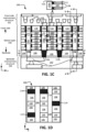
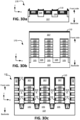
- Figs. 3C1, 3C2, and 3C3 are for formation of the structure 100, while Figs. 3Ca, 3Cb, and 3Cc are for formation of the structure 170.
- the method 200 proceeds from 212 to 216.
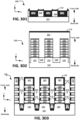
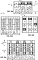
- gate spacers 110 abutting the channel material 103 are formed, and the material of the gate spacer 110 is also deposited (i) within sections of the source or drain trenches 314a, 314b, 314c, 314d (e.g., that extend within the sub-fin area) as dielectric material 114a, 114b, 114c, 114d, respectively, as illustrated in Fig.
- the gate spacers 110 are planarized (e.g., through a gate spacer etch process), such that the end sections of the nanoribbons 103 are exposed through the gate spacers 110 (e.g., see Fig. 3D3 or 3Dc ). Additionally, the dielectric material for the gate spacers 110 is also deposited in deeper sections of the trenches 314a, 314b, 314c, 314d (or trenches 314a', 314b', 314c', 314d'), to respectively form dielectric materials 114a, 114b, 114c, 114d, as illustrated in Fig. 3D3 and Fig. 3Dc .
- a height of the dielectric materials 114a, 114b, 114c, 114d in Fig. 3D3 is more than a height of the dielectric materials 114a, 114b, 114c, 114d in Fig. 3Dc , due to the above described height h2 being more than height h1.
- portions of the material of the gate spacers 110 e.g., the dielectric materials 114a, 114b, 114c, 114d
- the method 200 proceeds from 216 to 220.
- the source and drain regions 126 are formed, the dummy gate stacks 307 are removed, the nanoribbons 103 are released (e.g., by removing the sacrificial material 303), the final gate stack comprising the gate electrodes 112 and gate dielectric 128 are formed, the frontside gate contacts 116 are formed, the frontside source or drain contacts 125b, 125c are formed, and the frontside interconnect structure 102 is formed, e.g., using techniques to form at least sections of the device layer 150 comprising the GAA devices and the frontside interconnect structure 102, as illustrated in Figs. 3E1, 3E2, and 3E3 , and as also illustrated in Figs. 3Ea, 3Eb, and 3Ec .
- each of the source or drain regions 126a, ..., 126d has corresponding dielectric materials 114a, ..., 114d, respectively, there below, as illustrated in Fig. 3E3 and 3Ec .
- Each of the dielectric materials 114a, ..., 114d is laterally between two sub-fins 105.
- the method 200 proceeds from 220 to 224.
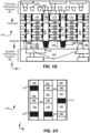
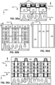
- the device wafer is bonded to a carrier, the bonded wafer is flipped, and the device substrate 107 is at least in part removed from the backside, as illustrated in Figs. 3F1, 3F2, 3F3, and 3F4 , and as also illustrated in Figs. 3Fa, 3Fb, 3Fc, and 3Fd .
- the dielectric materials 114a, ..., 114d are deeper in Figs. 3F1-3F4 , and hence, during the substrate 107 removal process, the lower surfaces of the dielectric materials 114a, ..., 114d are revealed in Figs. 3F1, 3F2, 3F3, and 3F4 .
- the dielectric materials 114a, ..., 114d is less deep in Figs. 3Fa-3Fd , and hence, during the substrate 107 removal process, the lower surfaces of the dielectric materials 114a, ..., 114d are not revealed in Figs. 3Fa, 3Fb, 3Fc, and 3Fd .
- the backside is above the frontside in the orientations of Figs. 3F1, 3F2, and 3F3 , and 3Fa, 3Fb, and 3Fc .
- the substrate is removed, for example with a mechanical polish process, or a chemical mechanical polish (CMP) process, or an etch process.
- CMP chemical mechanical polish
- the method 200 proceeds from 224 to 228.
- the material of the sub-fins 105 are at least partially replaced with corresponding dielectric material 106, as illustrated in Figs. 3G1, 3G2, 3G3, 3G4 , and as also illustrated in Figs. 3Ga, 3Gb, 3Gc, 3Gd .
- the STI 104 are visible, along with the dielectric material 106 and the dielectric materials 114 (such as dielectric materials 114a, ..., 114d).
- the dielectric material 114 such as dielectric materials 114a, ..., 114d.
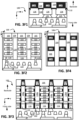
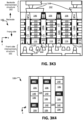
- a mask 320 is patterned on the backside, such that the mask 320 has openings above the dielectric material 114 coupled to one or more source or drain regions for which backside source or drain contacts are desired, as illustrated in 3H1, 3H2, 3H3 , and 3H4 , and as also illustrated in Figs. 3Ha, 3Hb, 3Hc, and 3Hd .
- Fig. 1 Fig. 1
- 3H3 illustrates openings within the mask 320 above the dielectric materials 114a, 114d of the source or drain regions 114a, 114d, respectively, wherein backside source or drain contacts are desired for the source or drain regions 114a, 114d.
- the mask 320 is illustrated to mask one or more instances of the dielectric material 114, while exposing one or more other instances of the dielectric material 114.
- Figs. 3Ha-3Hd although the openings within the mask 320 are above the dielectric materials 114a, 114d, respectively, the dielectric materials 114a, 114d are not exposed through the openings, for being covered by the dielectric material 106.
- the mask 320 may be of any appropriate type, and may include one or more layers (such as a tri-layer mask).
- the mask 320 comprises titanium nitride (TiN), tungsten doped carbide, or a carbon based hard mask, for example.
- TiN titanium nitride
- tungsten doped carbide or a carbon based hard mask, for example.
- the mask 320 defines openings for backside source or drain contacts.
- the method 200 proceeds from 232 to 236.
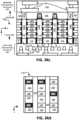
- one or more instances of the dielectric material 114 are removed (e.g., to form corresponding recesses 324) through the openings within the mask 320, while one or more other instances of the dielectric material 114 covered by mask 320 are not removed, as illustrated in Figs. 3I1, 3I2, 3I3 , and 3I4 , and as also illustrated in Figs. 3Ia, 3Ib, 3Ic, 3Id , 3Ie, 3If, 3Ig, and 3Ih .
- the dielectric material 114a, 114d exposed through the openings within the mask 320 are removed, e.g., etched, to form recesses 324.
- the recesses 324 are self-aligned to the corresponding source or drain regions 126.
- the recess 324a is self-aligned to the corresponding source or drain region 126a
- the recess 324b is self-aligned to the corresponding source or drain region 126b. This consequently results in the later formed source or drain contacts 140a, 140b being self-aligned to the source or drain regions 126a, 126d, respectively.
- the dielectric material 114a, 114d are removed using two different removal processes.
- sections of the dielectric material 106, which are above the dielectric materials 114a, 114d and which are exposed through the openings within the masks 320 are removed initially, thereby exposing the dielectric materials 114a, 114d through the openings within the masks 320.
- the dielectric material 114a, 114d exposed through the openings within the mask 320 are removed. Because of the two different etch processes in Figs.
- the sidewalls of the recesses 324a, 324d are stepped, which eventually results in the sidewalls of the source or drain contacts 180a, 180d being also stepped (see Fig. 1G ). Note that the recesses 324 are self-aligned to the corresponding source or drain regions 126.
- Figs. 3I3 and 3Ig illustrate dielectric material 114a being removed, resulting in recess 324a, and hence, the source or drain region 126a being exposed from the backside through the recess 324a.
- Figs. 3I3 and 3Ig also illustrate dielectric material 114d being removed, resulting in recess 324d, and hence, the source or drain region 126d being exposed from the backside through the recess 324d.
- the source or drain regions 126b, 126c are covered by the dielectric materials 114b, 114c, respectively, as the dielectric materials 114b, 114c are not removed for being covered by the mask 320. Note that the etch process may round off some of the surrounding dielectric material, such as dielectric material 106.
- the method 200 proceeds from 236 to 240.
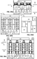
- the mask 320 is removed, and conductive material is deposited within the recesses 324 formed by selective removal of the dielectric material 114 and planarized to the top surface of dielectrics 104 and 106 (e.g., where the planarization is within a tolerance of at most 5 nm, or at most 3 nm, or at most 2 nm, or at most 1 nm, for example), as illustrated in Figs. 3J1, 3J2, 3J3, and 3J4 , and as also illustrated in Figs. 3Ja, 3Jb, 3Jc, and 3Jd .
- deposition of the conductive materials results in formation of the backside source or drain contacts 140a and 140b respectively coupled to the source or drain regions 126a, 126b, as illustrated in Fig. 3J3 , or formation of the backside source or drain contacts 180a and 180b respectively coupled to the source or drain regions 126a, 126b, as illustrated in Fig. 3Jc .
- Note the stepped sidewalls of the backside source or drain contacts 180a and 180b of Fig. 3Jc due to the above described two step removal process 236 described above.
- Example conductive material for the backside source or drain contacts have been described above.
- the communication chip 1006 may implement any of a number of wireless standards or protocols, including, but not limited to, Wi-Fi (IEEE 802.11 family), WiMAX (IEEE 802.16 family), IEEE 802.20, long term evolution (LTE), Ev-DO, HSPA+, HSDPA+, HSUPA+, EDGE, GSM, GPRS, CDMA, TDMA, DECT, Bluetooth, derivatives thereof, as well as any other wireless protocols that are designated as 3G, 4G, 5G, and beyond.
- the computing system 1000 may include a plurality of communication chips 1006.
- Example 3 The integrated circuit structure of any one of examples 1-2, further comprising: a third source or drain contact coupled to a frontside of a third source or drain region of the plurality of source and drain regions; and a third dielectric material coupled to a backside of the third source or drain region, wherein lower surfaces of each of the second dielectric material, the second source or drain contact, and the third dielectric material are coplanar within a tolerance of at most 5 nanometers (nm).
- Example 8 The integrated circuit structure of any one of examples 1-7, wherein the second source or drain contact comprises: a stepped sidewall having a first section and a second section, wherein the first section is stepped inward of the second section of the sidewall so as to provide a step section of the stepped sidewall, the step section extending more in the horizontal direction than in the vertical direction.
- Example 15 The integrated circuit structure of any one of examples 11-14, wherein each of the first and second dielectric materials comprises silicon, and one or more of oxygen, nitrogen, and carbon.
- Example 16 A method comprising: forming a first source or drain trench and a second source or drain trench, wherein the first and second source or drain trenches extend within respective sub-fin regions, and wherein a first end of a body is exposed through the first source or drain trench, and a second end of the body is exposed through the second source or drain trench, the body comprising a semiconductor material; depositing a first dielectric material within the first source or drain trench, to form (i) a first gate spacer that wraps around the first end of the body, and (ii) a portion of the first dielectric material at a lower section of the first source or drain trench extending within the sub-fin region; depositing a second dielectric material within the second source or drain trench, to form (i) a second gate spacer that wraps around the second end of the body, and (ii) a portion of the second dielectric material at a lower section of the second source or drain trench extending within the sub-fin region; forming a first source or drain region within the first
- Example 19 The method of example 18, wherein removing the portion of the second dielectric material comprises: patterning a mask on the backside of the second source or drain region, the mask having an opening above the portion of the second dielectric material, and the mask covering the portion of the first dielectric material; and removing, through the opening within the mask, the portion of the second dielectric material.
Landscapes
- Insulated Gate Type Field-Effect Transistor (AREA)
- Thin Film Transistor (AREA)
Applications Claiming Priority (1)
| Application Number | Priority Date | Filing Date | Title |
|---|---|---|---|
| US18/400,472 US20250220959A1 (en) | 2023-12-29 | 2023-12-29 | Front side and backside source or drain contacts |
Publications (1)
| Publication Number | Publication Date |
|---|---|
| EP4580338A1 true EP4580338A1 (de) | 2025-07-02 |
Family
ID=93258963
Family Applications (1)
| Application Number | Title | Priority Date | Filing Date |
|---|---|---|---|
| EP24208309.5A Pending EP4580338A1 (de) | 2023-12-29 | 2024-10-23 | Vorderseitige und rückseitige source- oder drain-kontakte |
Country Status (2)
| Country | Link |
|---|---|
| US (1) | US20250220959A1 (de) |
| EP (1) | EP4580338A1 (de) |
Cited By (1)
| Publication number | Priority date | Publication date | Assignee | Title |
|---|---|---|---|---|
| US20230402507A1 (en) * | 2022-06-13 | 2023-12-14 | Intel Corporation | Dual metal silicide for stacked transistor devices |
Citations (2)
| Publication number | Priority date | Publication date | Assignee | Title |
|---|---|---|---|---|
| US20220359679A1 (en) * | 2021-05-05 | 2022-11-10 | Taiwan Semiconductor Manufacturing Co., Ltd. | Backside source/drain contacts and methods of forming the same |
| US20230290825A1 (en) * | 2022-03-11 | 2023-09-14 | Intel Corporation | Integrated circuit structures with backside self-aligned conductive source or drain contact |
-
2023
- 2023-12-29 US US18/400,472 patent/US20250220959A1/en active Pending
-
2024
- 2024-10-23 EP EP24208309.5A patent/EP4580338A1/de active Pending
Patent Citations (2)
| Publication number | Priority date | Publication date | Assignee | Title |
|---|---|---|---|---|
| US20220359679A1 (en) * | 2021-05-05 | 2022-11-10 | Taiwan Semiconductor Manufacturing Co., Ltd. | Backside source/drain contacts and methods of forming the same |
| US20230290825A1 (en) * | 2022-03-11 | 2023-09-14 | Intel Corporation | Integrated circuit structures with backside self-aligned conductive source or drain contact |
Cited By (1)
| Publication number | Priority date | Publication date | Assignee | Title |
|---|---|---|---|---|
| US20230402507A1 (en) * | 2022-06-13 | 2023-12-14 | Intel Corporation | Dual metal silicide for stacked transistor devices |
Also Published As
| Publication number | Publication date |
|---|---|
| US20250220959A1 (en) | 2025-07-03 |
Similar Documents
| Publication | Publication Date | Title |
|---|---|---|
| US20230402513A1 (en) | Source and drain contacts formed using sacrificial regions of source and drain | |
| EP4199063A1 (de) | Gestapelte transistoren mit entfernter epi-barriere | |
| TWI770052B (zh) | 包括採用雙電荷摻雜劑之源極/汲極的電晶體 | |
| US20230395718A1 (en) | 3d source and drain contacts tuned for vertically stacked pmos and nmos | |
| EP4177938A1 (de) | Gitterstapel zur herstellung eines internen abstandshalters | |
| EP4202996A2 (de) | Kointegration von hochspannungs- und niederspannungstransistorstrukturen mit kanalhöhen- und abstandsmodulation | |
| EP4199062A1 (de) | Nichtreaktiver epi-kontakt für gestapelte transistoren | |
| EP4626179A1 (de) | Gabelfolientransistoren mit selbstausgerichteter dielektrischer wirbelsäule | |
| US20230132749A1 (en) | Stepwise internal spacers for stacked transistor structures | |
| EP4580338A1 (de) | Vorderseitige und rückseitige source- oder drain-kontakte | |
| US20230402507A1 (en) | Dual metal silicide for stacked transistor devices | |
| KR20230083216A (ko) | 비평면형 트랜지스터의 리세스된 내부 게이트 스페이서 및 부분적 대체 채널 | |
| EP4568449A2 (de) | Duale einachsige dehnung in bandförmigen kanälen | |
| CN115939137A (zh) | 多层多功能间隔物堆叠 | |
| EP4345869A1 (de) | Metallgate-schnitt nach bildung der source- und drainkontakte | |
| US20240222447A1 (en) | Gate cut, and source and drain contacts | |
| US12550373B2 (en) | Selective removal of channel bodies in stacked gate-all-around (GAA) device structures | |
| US20240071831A1 (en) | Source and drain regions for laterally adjacent gate-all-around (gaa) pmos and nmos | |
| EP4391066A1 (de) | Länglicher kontakt für source- oder drainbereich | |
| EP4345877A1 (de) | Torschnitt mit asymmetrischem kanal-zu-torschnittabstand | |
| US20240213026A1 (en) | Chemical mechanical polishing of metal gate cuts formed after source and drain contacts | |
| EP4661619A1 (de) | Unterlamellentechnik zur verbesserung der leistungsfähigkeit einer halbleitervorrichtung | |
| US20240088134A1 (en) | Targeted sub-fin etch depth | |
| EP4709082A1 (de) | Selbstjustierter gate-schnitt mit hybrider architektur | |
| US20240088133A1 (en) | Transistor devices with integrated diodes |
Legal Events
| Date | Code | Title | Description |
|---|---|---|---|
| PUAI | Public reference made under article 153(3) epc to a published international application that has entered the european phase |
Free format text: ORIGINAL CODE: 0009012 |
|
| STAA | Information on the status of an ep patent application or granted ep patent |
Free format text: STATUS: THE APPLICATION HAS BEEN PUBLISHED |
|
| AK | Designated contracting states |
Kind code of ref document: A1 Designated state(s): AL AT BE BG CH CY CZ DE DK EE ES FI FR GB GR HR HU IE IS IT LI LT LU LV MC ME MK MT NL NO PL PT RO RS SE SI SK SM TR |
|
| STAA | Information on the status of an ep patent application or granted ep patent |
Free format text: STATUS: REQUEST FOR EXAMINATION WAS MADE |
|
| 17P | Request for examination filed |
Effective date: 20260102 |