EP4580332A1 - Integrierte schaltungsstruktur mit asymmetrischen epitaktischen source- oder drain-, sowie spacer- anordnungen - Google Patents
Integrierte schaltungsstruktur mit asymmetrischen epitaktischen source- oder drain-, sowie spacer- anordnungen Download PDFInfo
- Publication number
- EP4580332A1 EP4580332A1 EP24207744.4A EP24207744A EP4580332A1 EP 4580332 A1 EP4580332 A1 EP 4580332A1 EP 24207744 A EP24207744 A EP 24207744A EP 4580332 A1 EP4580332 A1 EP 4580332A1
- Authority
- EP
- European Patent Office
- Prior art keywords
- gate
- drain
- contact
- epitaxial source
- layer
- Prior art date
- Legal status (The legal status is an assumption and is not a legal conclusion. Google has not performed a legal analysis and makes no representation as to the accuracy of the status listed.)
- Pending
Links
Images









Classifications
-
- H—ELECTRICITY
- H10—SEMICONDUCTOR DEVICES; ELECTRIC SOLID-STATE DEVICES NOT OTHERWISE PROVIDED FOR
- H10D—INORGANIC ELECTRIC SEMICONDUCTOR DEVICES
- H10D30/00—Field-effect transistors [FET]
- H10D30/60—Insulated-gate field-effect transistors [IGFET]
- H10D30/67—Thin-film transistors [TFT]
- H10D30/6757—Thin-film transistors [TFT] characterised by the structure of the channel, e.g. transverse or longitudinal shape or doping profile
-
- H—ELECTRICITY
- H10—SEMICONDUCTOR DEVICES; ELECTRIC SOLID-STATE DEVICES NOT OTHERWISE PROVIDED FOR
- H10D—INORGANIC ELECTRIC SEMICONDUCTOR DEVICES
- H10D30/00—Field-effect transistors [FET]
- H10D30/501—FETs having stacked nanowire, nanosheet or nanoribbon channels
-
- H—ELECTRICITY
- H10—SEMICONDUCTOR DEVICES; ELECTRIC SOLID-STATE DEVICES NOT OTHERWISE PROVIDED FOR
- H10D—INORGANIC ELECTRIC SEMICONDUCTOR DEVICES
- H10D30/00—Field-effect transistors [FET]
- H10D30/01—Manufacture or treatment
- H10D30/019—Manufacture or treatment of FETs having stacked nanowire, nanosheet or nanoribbon channels
-
- H—ELECTRICITY
- H10—SEMICONDUCTOR DEVICES; ELECTRIC SOLID-STATE DEVICES NOT OTHERWISE PROVIDED FOR
- H10D—INORGANIC ELECTRIC SEMICONDUCTOR DEVICES
- H10D30/00—Field-effect transistors [FET]
- H10D30/01—Manufacture or treatment
- H10D30/019—Manufacture or treatment of FETs having stacked nanowire, nanosheet or nanoribbon channels
- H10D30/0195—Manufacture or treatment of FETs having stacked nanowire, nanosheet or nanoribbon channels forming inner spacers between adjacent channels, e.g. changing their shapes or sizes
- H10D30/0197—Manufacture or treatment of FETs having stacked nanowire, nanosheet or nanoribbon channels forming inner spacers between adjacent channels, e.g. changing their shapes or sizes the inner spacers having different properties
-
- H—ELECTRICITY
- H10—SEMICONDUCTOR DEVICES; ELECTRIC SOLID-STATE DEVICES NOT OTHERWISE PROVIDED FOR
- H10D—INORGANIC ELECTRIC SEMICONDUCTOR DEVICES
- H10D30/00—Field-effect transistors [FET]
- H10D30/40—FETs having zero-dimensional [0D], one-dimensional [1D] or two-dimensional [2D] charge carrier gas channels
- H10D30/43—FETs having zero-dimensional [0D], one-dimensional [1D] or two-dimensional [2D] charge carrier gas channels having one-dimensional [1D] charge carrier gas channels, e.g. quantum wire FETs or transistors having 1D quantum-confined channels
-
- H—ELECTRICITY
- H10—SEMICONDUCTOR DEVICES; ELECTRIC SOLID-STATE DEVICES NOT OTHERWISE PROVIDED FOR
- H10D—INORGANIC ELECTRIC SEMICONDUCTOR DEVICES
- H10D30/00—Field-effect transistors [FET]
- H10D30/501—FETs having stacked nanowire, nanosheet or nanoribbon channels
- H10D30/507—FETs having stacked nanowire, nanosheet or nanoribbon channels characterised by inner spacers between adjacent channels
- H10D30/508—FETs having stacked nanowire, nanosheet or nanoribbon channels characterised by inner spacers between adjacent channels characterised by the relative sizes, shapes or dispositions of the inner spacers
-
- H—ELECTRICITY
- H10—SEMICONDUCTOR DEVICES; ELECTRIC SOLID-STATE DEVICES NOT OTHERWISE PROVIDED FOR
- H10D—INORGANIC ELECTRIC SEMICONDUCTOR DEVICES
- H10D62/00—Semiconductor bodies, or regions thereof, of devices having potential barriers
- H10D62/10—Shapes, relative sizes or dispositions of the regions of the semiconductor bodies; Shapes of the semiconductor bodies
- H10D62/113—Isolations within a component, i.e. internal isolations
- H10D62/115—Dielectric isolations, e.g. air gaps
- H10D62/116—Dielectric isolations, e.g. air gaps adjoining the input or output regions of field-effect devices, e.g. adjoining source or drain regions
-
- H—ELECTRICITY
- H10—SEMICONDUCTOR DEVICES; ELECTRIC SOLID-STATE DEVICES NOT OTHERWISE PROVIDED FOR
- H10D—INORGANIC ELECTRIC SEMICONDUCTOR DEVICES
- H10D62/00—Semiconductor bodies, or regions thereof, of devices having potential barriers
- H10D62/10—Shapes, relative sizes or dispositions of the regions of the semiconductor bodies; Shapes of the semiconductor bodies
- H10D62/13—Semiconductor regions connected to electrodes carrying current to be rectified, amplified or switched, e.g. source or drain regions
- H10D62/149—Source or drain regions of field-effect devices
- H10D62/151—Source or drain regions of field-effect devices of IGFETs
-
- H—ELECTRICITY
- H10—SEMICONDUCTOR DEVICES; ELECTRIC SOLID-STATE DEVICES NOT OTHERWISE PROVIDED FOR
- H10D—INORGANIC ELECTRIC SEMICONDUCTOR DEVICES
- H10D62/00—Semiconductor bodies, or regions thereof, of devices having potential barriers
- H10D62/10—Shapes, relative sizes or dispositions of the regions of the semiconductor bodies; Shapes of the semiconductor bodies
- H10D62/17—Semiconductor regions connected to electrodes not carrying current to be rectified, amplified or switched, e.g. channel regions
- H10D62/351—Substrate regions of field-effect devices
- H10D62/357—Substrate regions of field-effect devices of FETs
- H10D62/364—Substrate regions of field-effect devices of FETs of IGFETs
-
- H—ELECTRICITY
- H10—SEMICONDUCTOR DEVICES; ELECTRIC SOLID-STATE DEVICES NOT OTHERWISE PROVIDED FOR
- H10D—INORGANIC ELECTRIC SEMICONDUCTOR DEVICES
- H10D64/00—Electrodes of devices having potential barriers
- H10D64/01—Manufacture or treatment
- H10D64/017—Manufacture or treatment using dummy gates in processes wherein at least parts of the final gates are self-aligned to the dummy gates, i.e. replacement gate processes
-
- H—ELECTRICITY
- H10—SEMICONDUCTOR DEVICES; ELECTRIC SOLID-STATE DEVICES NOT OTHERWISE PROVIDED FOR
- H10D—INORGANIC ELECTRIC SEMICONDUCTOR DEVICES
- H10D64/00—Electrodes of devices having potential barriers
- H10D64/20—Electrodes characterised by their shapes, relative sizes or dispositions
- H10D64/23—Electrodes carrying the current to be rectified, amplified, oscillated or switched, e.g. sources, drains, anodes or cathodes
- H10D64/251—Source or drain electrodes for field-effect devices
- H10D64/254—Source or drain electrodes for field-effect devices for lateral devices wherein the source or drain electrodes extend entirely through the semiconductor bodies, e.g. via-holes for back side contacts
-
- H—ELECTRICITY
- H10—SEMICONDUCTOR DEVICES; ELECTRIC SOLID-STATE DEVICES NOT OTHERWISE PROVIDED FOR
- H10D—INORGANIC ELECTRIC SEMICONDUCTOR DEVICES
- H10D64/00—Electrodes of devices having potential barriers
- H10D64/20—Electrodes characterised by their shapes, relative sizes or dispositions
- H10D64/23—Electrodes carrying the current to be rectified, amplified, oscillated or switched, e.g. sources, drains, anodes or cathodes
- H10D64/251—Source or drain electrodes for field-effect devices
- H10D64/256—Source or drain electrodes for field-effect devices for lateral devices wherein the source or drain electrodes are recessed in semiconductor bodies
-
- B—PERFORMING OPERATIONS; TRANSPORTING
- B82—NANOTECHNOLOGY
- B82Y—SPECIFIC USES OR APPLICATIONS OF NANOSTRUCTURES; MEASUREMENT OR ANALYSIS OF NANOSTRUCTURES; MANUFACTURE OR TREATMENT OF NANOSTRUCTURES
- B82Y10/00—Nanotechnology for information processing, storage or transmission, e.g. quantum computing or single electron logic
-
- H—ELECTRICITY
- H10—SEMICONDUCTOR DEVICES; ELECTRIC SOLID-STATE DEVICES NOT OTHERWISE PROVIDED FOR
- H10D—INORGANIC ELECTRIC SEMICONDUCTOR DEVICES
- H10D30/00—Field-effect transistors [FET]
- H10D30/60—Insulated-gate field-effect transistors [IGFET]
- H10D30/67—Thin-film transistors [TFT]
- H10D30/6729—Thin-film transistors [TFT] characterised by the electrodes
- H10D30/673—Thin-film transistors [TFT] characterised by the electrodes characterised by the shapes, relative sizes or dispositions of the gate electrodes
- H10D30/6735—Thin-film transistors [TFT] characterised by the electrodes characterised by the shapes, relative sizes or dispositions of the gate electrodes having gates fully surrounding the channels, e.g. gate-all-around
-
- H—ELECTRICITY
- H10—SEMICONDUCTOR DEVICES; ELECTRIC SOLID-STATE DEVICES NOT OTHERWISE PROVIDED FOR
- H10D—INORGANIC ELECTRIC SEMICONDUCTOR DEVICES
- H10D62/00—Semiconductor bodies, or regions thereof, of devices having potential barriers
- H10D62/10—Shapes, relative sizes or dispositions of the regions of the semiconductor bodies; Shapes of the semiconductor bodies
- H10D62/117—Shapes of semiconductor bodies
- H10D62/118—Nanostructure semiconductor bodies
- H10D62/119—Nanowire, nanosheet or nanotube semiconductor bodies
- H10D62/121—Nanowire, nanosheet or nanotube semiconductor bodies oriented parallel to substrates
Definitions
- Tri-gate transistors In the manufacture of integrated circuit devices, multi-gate transistors, such as tri-gate transistors, have become more prevalent as device dimensions continue to scale down. Tri-gate transistors are generally fabricated on either bulk silicon substrates or silicon-on-insulator substrates. In some instances, bulk silicon substrates are preferred due to their lower cost and compatibility with the existing high-yielding bulk silicon substrate infrastructure.
- Coupled means that one element or node or feature is directly or indirectly joined to (or directly or indirectly communicates with) another element or node or feature, and not necessarily mechanically.
- inhibit is used to describe a reducing or minimizing effect. When a component or feature is described as inhibiting an action, motion, or condition it may completely prevent the result or outcome or future state completely. Additionally, “inhibit” can also refer to a reduction or lessening of the outcome, performance, or effect which might otherwise occur. Accordingly, when a component, element, or feature is referred to as inhibiting a result or state, it need not completely prevent or eliminate the result or state.
- Embodiments described herein may be directed to front-end-of-line (FEOL) semiconductor processing and structures.
- FEOL is the first portion of integrated circuit (IC) fabrication where the individual devices (e.g., transistors, capacitors, resistors, etc.) are patterned in the semiconductor substrate or layer.
- FEOL generally covers everything up to (but not including) the deposition of metal interconnect layers. Following the last FEOL operation, the result is typically a wafer with isolated transistors (e.g., without any wires).
- Embodiments described herein may be directed to back-end-of-line (BEOL) semiconductor processing and structures.
- BEOL is the second portion of IC fabrication where the individual devices (e.g., transistors, capacitors, resistors, etc.) get interconnected with wiring on the wafer, e.g., the metallization layer or layers.
- BEOL includes contacts, insulating layers (dielectrics), metal levels, and bonding sites for chip-to-package connections.
- contacts pads
- interconnect wires, vias and dielectric structures are formed. For modern IC processes, more than 10 metal layers may be added in the BEOL.
- Embodiments described below may be applicable to FEOL processing and structures, BEOL processing and structures, or both FEOL and BEOL processing and structures.
- an exemplary processing scheme may be illustrated using a FEOL processing scenario, such approaches may also be applicable to BEOL processing.
- an exemplary processing scheme may be illustrated using a BEOL processing scenario, such approaches may also be applicable to FEOL processing.
- One or more embodiments are directed to structures including asymmetric gate spacers with increased front side drain spacer thickness.
- One or more embodiments are directed to structures including asymmetric doped tips via front side and backside contact processing.
- One or more embodiments described herein are directed to gate-all-around integrated circuit structures fabricated to have asymmetric epitaxial source or drain arrangements. It is to be appreciated that, unless indicated otherwise, reference to nanowires herein can indicate nanowires or nanoribbons or nanosheets or forksheets.
- One or more embodiments described herein are directed to fin-based integrated circuit structures fabricated to have asymmetric epitaxial source or drain arrangements.
- backside processing of logic transistor technologies allows for separate patterning and etching of source side contacts versus topside drain contacts.
- having an asymmetric spacer with thicker spacer on the drain contacts allows for lower parasitic capacitance and a thinner spacer on the source backside contact allows for improved contact resistance without a capacitive penalty because there is no backside gate contact.
- Advantages for implementing embodiments described herein can include increased performance due to (1) lower parasitic capacitance, (2) lower source side tip resistance, (3) improved shorting margin for wide drain spacer, and/or (4) reduced short channel effects.
- Detection of the implementation of embodiments described herein can include TEM or SEM imaging.
- a specific difference in widths of the source (backside) and drain spacers alongside the data may clearly be captured in a SEM or TEM image and the thicknesses can be measured. The asymmetric nature may be visually capture and compared.
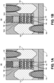
- Figure 1A illustrates a cross-sectional view representing an integrated circuit structure having symmetric gate spacers
- Figure 1B illustrates a cross-sectional view representing an integrated circuit structure having asymmetric gate spacers, in accordance with an embodiment of the present disclosure.
- an integrated circuit structure 100 includes a sub-fin structure 102 on a backside dielectric layer 101, such as a silicon sub-fin structure on a silicon oxide or silicon dioxide backside dielectric layer.
- a vertical stack of horizontal nanowires 104 such as silicon nanowires, is over the sub-fin structure 104.
- a gate stack 106/108 such as a stack including a high-k gate dielectric layer 106 and a metal gate electrode 108, is over and around the vertical stack of horizontal nanowires 104.
- Gate spacers 114A and 114B such as silicon nitride gate spacers, are adjacent to a source side and a drain side, respectively, of the gate stack 106/108.
- An epitaxial source structure 110 and an epitaxial drain structure 112 are at corresponding ends of the vertical stack of horizontal nanowires 104 and adjacent to the gate spacers 114A and 114B.
- a front side gate contact 116 is on the gate electrode 108
- a backside source contact 118 is on the epitaxial source structure 110
- a front side drain contact 120 is on the epitaxial drain structure 112.
- the source side gate spacer 114A has a same width as the drain side gate spacer 114B.
- the epitaxial source structure 110 is a same lateral distance from the gate electrode 108 as the epitaxial drain structure 112.
- an integrated circuit structure 150 includes a sub-fin structure 152 on a backside dielectric layer 151, such as a silicon sub-fin structure on a silicon oxide or silicon dioxide backside dielectric layer.
- a vertical stack of horizontal nanowires 154 such as silicon nanowires, is over the sub-fin structure 154.
- a gate stack 156/158 such as a stack including a high-k gate dielectric layer 156 and a metal gate electrode 158, is over and around the vertical stack of horizontal nanowires 154.
- Gate spacers 164A and 164B such as silicon nitride gate spacers, are adjacent to a source side and a drain side, respectively, of the gate stack 156/158.
- An epitaxial source structure 160 and an epitaxial drain structure 162 are at corresponding ends of the vertical stack of horizontal nanowires 154 and adjacent to the gate spacers 164A and 164B.
- a front side gate contact 166 is on the gate electrode 158
- a backside source contact 168 is on the epitaxial source structure 160
- a front side drain contact 170 is on the epitaxial drain structure 162.
- the source side gate spacer 164A has a width less than a width of the drain side gate spacer 164B.
- the epitaxial source structure 160 is a lesser lateral distance from the gate electrode 158 than the epitaxial drain structure 162.
- the source side gate spacer 164A has a width less than a width of the drain side gate spacer 164B, e.g., by an amount of 10% or greater.
- the epitaxial source structure 160 and the epitaxial drain structure 162 are composed of silicon, germanium and boron, e.g., such as is found in PMOS source or drain structures. In another embodiment, the epitaxial source structure 160 and the epitaxial drain structure 162 are composed of silicon and phosphorous, e.g., such as is found in NMOS source or drain structures.
- structure 100 of Figure 1A has symmetric source and drain side spacers.
- Structure 150 of Figure 1B has a drain side spacer wider than a source side spacer.
- backside contact processing allows for separate and self-aligned processing for source and drain.
- Drain side capacitance can be more dominant than source side capacitance in setting parasitics.
- structures including structures including asymmetric doped tips via front side and backside contact processing are described.
- front side and backside patterning is leveraged to drive the doped tip extension under the gate farther in the source side and pull the tip away from the gate in the source side. This can provide a source side resistance reduction and a drain side capacitance reduction resulting in improved transistor performance.
- Advantages for implementing embodiments described herein can include lower resistance and capacitance resulting in improved transistor efficiency and performance.
- Detection of the implementation of embodiments described herein can include a combination of TEM and SIMS or TEM and APT to detect the asymmetric nature of the doping in the tip region and that it is farther under the gate spacer in the source side than in the drain side.
- Figure 2A illustrates a cross-sectional view representing an integrated circuit structure having symmetric tips
- Figure 2B illustrates a cross-sectional view representing an integrated circuit structure having asymmetric tips, in accordance with an embodiment of the present disclosure.
- an integrated circuit structure 200 includes a sub-fin structure 202 on a backside dielectric layer 201, such as a silicon sub-fin structure on a silicon oxide or silicon dioxide backside dielectric layer.
- a vertical stack of horizontal nanowires 204 such as silicon nanowires, is over the sub-fin structure 204.
- a gate stack 206/208 such as a stack including a high-k gate dielectric layer 206 and a metal gate electrode 208, is over and around the vertical stack of horizontal nanowires 204.
- Gate spacers 214A and 214B such as silicon nitride gate spacers, are adjacent to a source side and a drain side, respectively, of the gate stack 206/208.
- the vertical stack of horizontal nanowires 204 is recessed laterally relative to the gate spacers 214A and 214B.
- An epitaxial source structure 210 and an epitaxial drain structure 212 are at corresponding ends of the vertical stack of horizontal nanowires 204 and adjacent to the gate spacers 214A and 214B.
- the epitaxial source structure 210 has tips 210A that fill the recesses of the vertical stack of horizontal nanowires 204 on the source side.
- the epitaxial drain structure 212 has tips 212A that fill the recesses of the vertical stack of horizontal nanowires 204 on the drain side.
- a front side gate contact 216 is on the gate electrode 208, a backside source contact 218 is on the epitaxial source structure 210, and a front side drain contact 220 is on the epitaxial drain structure 212.
- the vertical stack of horizontal nanowires 204 is recessed laterally to the same extent at the source side 205A and at the drain side 205B.
- the tips 210A of the epitaxial source structure 210 have a same lateral width as the tips 212A of the epitaxial drain structure 212.
- an integrated circuit structure 250 includes a sub-fin structure 252 on a backside dielectric layer 251, such as a silicon sub-fin structure on a silicon oxide or silicon dioxide backside dielectric layer.
- a vertical stack of horizontal nanowires 254, such as silicon nanowires, is over the sub-fin structure 252.
- a gate stack 256/258 such as a stack including a high-k gate dielectric layer 256 and a metal gate electrode 258, is over and around the vertical stack of horizontal nanowires 254.
- Gate spacers 264A and 264B such as silicon nitride gate spacers, are adjacent to a source side and a drain side, respectively, of the gate stack 256/258.
- the vertical stack of horizontal nanowires 254 is recessed laterally relative to the gate spacers 264A and 264B.
- An epitaxial source structure 260 and an epitaxial drain structure 262 are at corresponding ends of the vertical stack of horizontal nanowires 254 and adjacent to the gate spacers 264A and 264B.
- the epitaxial source structure 260 has tips 260A that fill the recesses of the vertical stack of horizontal nanowires 254 on the source side.
- the epitaxial drain structure 262 has tips 262A that fill the recesses of the vertical stack of horizontal nanowires 254 on the drain side.
- a front side gate contact 266 is on the gate electrode 258, a backside source contact 268 is on the epitaxial source structure 260, and a front side drain contact 270 is on the epitaxial drain structure 262.
- the vertical stack of horizontal nanowires 254 is recessed laterally to a greater extent at the source side 255A than at the drain side 255B.
- the tips 260A of the epitaxial source structure 260 have a greater lateral width than the tips 262A of the epitaxial drain structure 262.
- the tips 260A of the epitaxial source structure 260 have a greater lateral width than the tips 262A of the epitaxial drain structure 262, e.g., by an amount of 10% or greater.
- the epitaxial source structure 260 and the epitaxial drain structure 262 are composed of silicon, germanium and boron, e.g., such as is found in PMOS source or drain structures. In another embodiment, the epitaxial source structure 260 and the epitaxial drain structure 262 are composed of silicon and phosphorous, e.g., such as is found in NMOS source or drain structures.
- structure 200 of Figure 2A has symmetric source and drain side spacers.
- Structure 250 of Figure 1B has source side doped tips that are closer to a gate edge than for a drain side.
- backside contact processing allows for separate and self-aligned processing for source and drain. External resistance reduction can be more sensitive to the source side. Drain side capacitance can be more dominant than source side capacitance in setting parasitics.
- contact formation to the epitaxial source or drain structures can be from the front side, from the backside, or both, as is exemplified.
- low electrical resistance power delivery solutions are needed as semiconductor scaling continues to stress interconnects into increasingly tight spaces.
- Backside power delivery a scheme where a power delivery interconnect network connects directly to the transistors from the back of the wafer instead of sharing space with front side routing is a possible solution for future semiconductor technology generations.
- power is delivered from a front side interconnect.
- power can be delivered right on top of transistors or from a top and bottom cell boundary.
- Power delivered from a top and bottom cell boundary enables relatively shorter standard cell height with slightly higher power network resistance.
- a front side power network shares interconnect stack with signal routing and reduces signal routing tracks.
- top and bottom cell boundary power metal wires must be wide enough to reduce power network resistance and improve performance. This normally results in a cell height increase.
- delivering power from a wafer or substrate backside can be implemented to solve area and performance problems.
- a power delivery network from bump to the transistor required significant block resources.
- Such resource usage on the metal stack expressed itself in some process nodes as Standard Cell architectures with layout versioning or cell placement restrictions in the block level.
- eliminating the power delivery network from the front side metal stack allows free sliding cell placement in the block without power delivery complications and placement related delay timing variation.
- Figure 3 illustrates cross-sectional views of an interconnect stack having front side power delivery and of an interconnect stack having backside power delivery, in accordance with an embodiment of the present disclosure.
- an interconnect stack 300 having front side power delivery includes a transistor 302 and signal and power delivery metallization 304.
- the transistor 302 includes a bulk substrate 306, semiconductor fins 308, a terminal 310, and a device contact 312.
- the signal and power delivery metallization 304 includes conductive vias 314, conductive lines 316, and a metal bump 318.
- an interconnect stack 350 having backside power delivery includes a transistor 352, front side signal metallization 354A, and power delivery metallization 354B.
- the transistor 352 includes semiconductor nanowires or nanoribbons 358, a terminal 360, and a device contact 362, and a boundary deep via 363.
- the front side signal metallization 354A includes conductive vias 364A, conductive lines 366A, and a metal bump 368A.
- the power delivery metallization 354B includes conductive vias 364B, conductive lines 366B, and a metal bump 368B. It is to be appreciated that a backside power approach can also be implemented for structures including semiconductor fins.
- a fundamental component of a backside power delivery network is an electrically functional feature that interfaces the source or drain contacts of a transistor with the backside interconnect network. Therefore, there is a need for a design and method of fabricating an interface feature that is compatible with existing library cell design conventions and transistor contact process flows.
- backside access features for epitaxial source or drain structures are described.
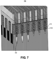
- Figures 4-9 illustrate angled cross-sectional views representing various operations in methods of fabricating an integrated circuit structure having differentiated backside source or drain contact access features, in accordance with an embodiment of the present disclosure. It is to be appreciated that the embodiments described and illustrated may also be applicable for a fin structure in place of a stack of nanowires or nanoribbons or nanosheets or forksheets. It is also to be appreciated that such an approach may be combined with asymmetric epitaxial source or drain arrangements, such as described above in association with Figures 1B and/or 2B.
- Dummy gate structures such as polysilicon 416 and silicon nitride 418 dummy gate structures (and, possibly dummy gate oxide 414), extend over the fins 408.
- Gate spacers 420 such as silicon nitride gate spacers, are over and along sides of the dummy gate structures.
- a protective helmet layer 422 such as a titanium helmet, is on tops of the gate spacers 420 as an artifact from an etch process used to etch the fins 408 in locations between gate structures, e.g., for eventual source or drain formation.
- the etch process is extended deeper than the fins 408 to form deep trenches 424 are etched into the sub-fins 404, as is depicted.
- etch process can be referred to as a self-aligned etch that is non-selective since deep trenches are formed in all locations.
- the release layers 412 are laterally recessed relative to the nanowires 410 to form recessed release layers 412A.
- An inner spacer material 432 such as silicon nitride inner spacer material, is formed in the recesses formed by recessed release layers 412A and on the contact placeholders 430 and dummy contact placeholders 428 to form structure 700.
- an asymmetric epitaxial source or drain arrangement approach such as described above in association with Figures 1B and/or 2B, can be implemented for all or select ones of the source or drain structures described in association with Figure 8 .
- structure 700 of Figure 7 is exposed to an epitaxial source or drain growth process, replacement gate and nanowire release process, inversion, and backside reveal process.
- the resulting structure includes a front side protecting dielectric layer 802, metal gate electrodes 804, high-k gate dielectrics 806, a gate cap (such as silicon nitride) 808, epitaxial source or drain structures (such as epitaxial silicon or epitaxial silicon germanium) 812 (which can be formed by patterning inner spacer material 432 to form placeholder caps 432A and inner spacers 432B), front side trench contact 814, dielectric sub-fin structures 816 (e.g., from replacement of silicon sub-fins), and dielectric gate cut plugs 818.
- the contact placeholders 430 are backside revealed to form planarized contact placeholders 430A.
- the dummy contact placeholders 428 are not revealed.
- the contact placeholders 430 and the placeholder caps 432A are removed and replaced with permanent backside contacts 902, such as cobalt or tungsten contacts, to form structure 900.
- the permanent backside contacts 902 contact corresponding ones 812A of source or drain structures 812.
- the dummy contact placeholders 428 remain with corresponding ones of the source or drain structures 812 that are not selected for backside contact.
- the permanent backside contacts 902 can ultimately be coupled to one or more backside metallization lines or layers.
- an integrated circuit structure 900 includes a first plurality of horizontally stacked nanowires or fin 412 laterally spaced apart from a second plurality of horizontally stacked nanowires or fin 412, the second plurality of horizontally stacked nanowires or fin 412 laterally spaced apart from a third plurality of horizontally stacked nanowires or fin 412.
- a first gate stack 804/806 is over the first plurality of horizontally stacked nanowires or fin 412
- a second gate stack 804/806 is over the second plurality of horizontally stacked nanowires or fin 412
- third gate stack 804/806 is over the third plurality of horizontally stacked nanowires or fin 412.
- a first epitaxial source or drain structure 812 is between the first plurality of horizontally stacked nanowires or fin 412 and the second plurality of horizontally stacked nanowires or fin 412, the first epitaxial source or drain structure 812 over a first conductive material 428 having a first depth below the first epitaxial source or drain structure 812.
- a second epitaxial source or drain structure 812A is between the second plurality of horizontally stacked nanowires or fin 412 and the third plurality of horizontally stacked nanowires or fin 412, the second epitaxial source or drain structure 812A over a second permanent backside contacts 902 having a second depth below the second epitaxial source or drain structure 812A, the second depth greater than the first depth.
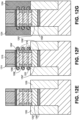
- the first conductive material and the second conductive material have different compositions.
- the first conductive material includes titanium and nitrogen
- the second conductive material includes tungsten or cobalt.
- a dielectric spacer cap is between the first epitaxial source or drain structure 812 and the first conductive material 428, as is depicted.
- the second permanent backside contacts 902 is in direct contact with the second epitaxial source or drain structure 812A, as is depicted.
- Cross-sections may show epitaxial structures of having different widths on respective sides of a gate structure. Cross-sections may show non-accessed or short contact "placeholders.” It is to be appreciated that even though the above Figures show gate-all-around-based transistors, embodiments can be applied to channels of any shape or material (fin, nanowire, nanoribbon, nanocomb/forksheet, etc.). It is to be appreciated that even though the Figures show a single layer of transistors, embodiments can be applied to multi-layer transistor architectures.
- a sub-fin, a nanowire, a nanoribbon, or a fin described herein may be a silicon sub-fin, a silicon nanowire, a silicon nanoribbon, or a silicon fin.
- a silicon layer or structure may be used to describe a silicon material composed of a very substantial amount of, if not all, silicon.
- 100% pure Si may be difficult to form and, hence, could include a tiny percentage of carbon, germanium or tin.
- Such impurities may be included as an unavoidable impurity or component during deposition of Si or may "contaminate" the Si upon diffusion during post deposition processing.
- embodiments described herein directed to a silicon layer or structure may include a silicon layer or structure that contains a relatively small amount, e.g., "impurity" level, non-Si atoms or species, such as Ge, C or Sn. It is to be appreciated that a silicon layer or structure as described herein may be undoped or may be doped with dopant atoms such as boron, phosphorous or arsenic.
- a sub-fin, a nanowire, a nanoribbon, or a fin described herein may be a silicon germanium sub-fin, a silicon germanium nanowire, a silicon germanium nanoribbon, or a silicon germanium fin.
- a silicon germanium layer or structure may be used to describe a silicon germanium material composed of substantial portions of both silicon and germanium, such as at least 5% of both.
- the amount of germanium is greater than the amount of silicon.
- a silicon germanium layer or structure includes approximately 60% germanium and approximately 40% silicon (Si 40 Ge 60 ). In other embodiments, the amount of silicon is greater than the amount of germanium.
- asymmetric epitaxial source or drain arrangements such as described above in association with Figures 1B and/or 2B, can be implemented with front side architectures.
- asymmetric epitaxial source or drain arrangements can be implemented with contact over active gate (COAG) structures and processes.
- COAG active gate
- "color" hardmask COAG features below can be applicable to concepts regarding the above described backside contacts.
- One or more embodiments of the present disclosure are directed to semiconductor structures or devices having one or more gate contact structures (e.g., as gate contact vias) disposed over active portions of gate electrodes of the semiconductor structures or devices.
- One or more embodiments of the present disclosure are directed to methods of fabricating semiconductor structures or devices having one or more gate contact structures formed over active portions of gate electrodes of the semiconductor structures or devices. Approaches described herein may be used to reduce a standard cell area by enabling gate contact formation over active gate regions.
- tapered gate and trench contacts are implemented to enable COAG fabrication.
- Embodiments may be implemented to enable patterning at tight pitches.
- a contact to gate structure may be fabricated by making contact to a portion of the gate electrode disposed over an isolation region.
- Figure 10A illustrates a plan view of a semiconductor device having a gate contact disposed over an inactive portion of a gate electrode.
- a semiconductor structure or device 1000A includes a diffusion or active region 1004 disposed in a substrate 1002, and within an isolation region 1006.
- One or more gate lines also known as poly lines
- gate lines 1008A, 1008B and 1008C are disposed over the diffusion or active region 1004 as well as over a portion of the isolation region 1006.
- Source or drain contacts also known as trench contacts
- Trench contact vias 1012A and 1012B provide contact to trench contacts 1010A and 1010B, respectively.
- a separate gate contact 1014, and overlying gate contact via 1016, provides contact to gate line 1008B.
- the gate contact 1014 is disposed, from a plan view perspective, over isolation region 1006, but not over diffusion or active region 1004. Furthermore, neither the gate contact 1014 nor gate contact via 1016 is disposed between the source or drain trench contacts 1010A and 1010B.
- Figure 10B illustrates a cross-sectional view of a non-planar semiconductor device having a gate contact disposed over an inactive portion of a gate electrode.
- a semiconductor structure or device 1000B e.g. a non-planar version of device 1000A of Figure 10A , includes a non-planar diffusion or active region 1004B (e.g., a fin structure) formed from substrate 1002, and within isolation region 1006.
- Gate line 1008B is disposed over the non-planar diffusion or active region 1004B as well as over a portion of the isolation region 1006.
- gate line 1008B includes a gate electrode 1050 and gate dielectric layer 1052, along with a dielectric cap layer 1054.
- Gate contact 1014, and overlying gate contact via 1016 are also seen from this perspective, along with an overlying metal interconnect 1060, all of which are disposed in inter-layer dielectric stacks or layers 1070. Also seen from the perspective of Figure 10B , the gate contact 1014 is disposed over isolation region 1006, but not over non-planar diffusion or active region 1004B.
- the arrangement of semiconductor structure or device 1000A and 1000B places the gate contact over isolation regions.
- Such an arrangement wastes layout space.
- placing the gate contact over active regions would require either an extremely tight registration budget or gate dimensions would have to increase to provide enough space to land the gate contact.
- contact to gate over diffusion regions has been avoided for risk of drilling through other gate material (e.g., polysilicon) and contacting the underlying active region.
- One or more embodiments described herein address the above issues by providing feasible approaches, and the resulting structures, to fabricating contact structures that contact portions of a gate electrode formed over a diffusion or active region.
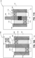
- Figure 11A illustrates a plan view of a semiconductor device having a gate contact via disposed over an active portion of a gate electrode, in accordance with an embodiment of the present disclosure.
- a semiconductor structure or device 1100A includes a diffusion or active region 1104 disposed in a substrate 1102, and within an isolation region 1106.
- One or more gate lines, such as gate lines 1108A, 1108B and 1108C are disposed over the diffusion or active region 1104 as well as over a portion of the isolation region 1106.
- Source or drain trench contacts, such as trench contacts 1110A and 1110B, are disposed over source and drain regions of the semiconductor structure or device 1100A.
- Trench contact vias 1112A and 1112B provide contact to trench contacts 11 10A and 11 10B, respectively.
- a gate contact via 1116 with no intervening separate gate contact layer, provides contact to gate line 1108B.
- the gate contact 1116 is disposed, from a plan view perspective, over the diffusion or active region 1104 and between the source or drain contacts 1110A and 1110B.
- gate line 1108B includes a gate electrode 1150 and gate dielectric layer 1152, along with a dielectric cap layer 1154.
- the gate contact via 1116 is also seen from this perspective, along with an overlying metal interconnect 1160, both of which are disposed in inter-layer dielectric stacks or layers 1170. Also seen from the perspective of Figure 11B , the gate contact via 1116 is disposed over non-planar diffusion or active region 1104B.
- a trench contact grid is not separately patterned, but is rather formed between poly (gate) lines.
- a trench contact grid is formed subsequent to gate grating patterning but prior to gate grating cuts.
- the gate stack structures may be fabricated by a replacement gate process.
- dummy gate material such as polysilicon or silicon nitride pillar material, may be removed and replaced with permanent gate electrode material.
- a permanent gate dielectric layer is also formed in this process, as opposed to being carried through from earlier processing.
- dummy gates are removed by a dry etch or wet etch process.
- dummy gates are composed of polycrystalline silicon or amorphous silicon and are removed with a dry etch process including SF 6 .
- a gate stack structure may be fabricated by a replacement gate process.
- dummy gate material such as polysilicon or silicon nitride pillar material, may be removed and replaced with permanent gate electrode material.
- a permanent gate dielectric layer is also formed in this process, as opposed to being carried through from earlier processing.
- dummy gates are removed by a dry etch or wet etch process.
- dummy gates are composed of polycrystalline silicon or amorphous silicon and are removed with a dry etch process including use of SF 6 .
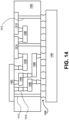
- FIG 14 illustrates an interposer 1400 that includes one or more embodiments of the disclosure.
- the interposer 1400 is an intervening substrate used to bridge a first substrate 1402 to a second substrate 1404.
- the first substrate 1402 may be, for instance, an integrated circuit die.
- the second substrate 1404 may be, for instance, a memory module, a computer motherboard, or another integrated circuit die.
- the purpose of an interposer 1400 is to spread a connection to a wider pitch or to reroute a connection to a different connection.
- an interposer 1400 may couple an integrated circuit die to a ball grid array (BGA) 1406 that can subsequently be coupled to the second substrate 1404.
- BGA ball grid array
- first and second substrates 1402/1404 are attached to opposing sides of the interposer 1400. In other embodiments, the first and second substrates 1402/1404 are attached to the same side of the interposer 1400. And in further embodiments, three or more substrates are interconnected by way of the interposer 1400.
- the interposer 1400 may include metal interconnects 1408 and vias 1410, including but not limited to through-silicon vias (TSVs) 1412.
- the interposer 1400 may further include embedded devices 1414, including both passive and active devices.
- Such devices include, but are not limited to, capacitors, decoupling capacitors, resistors, inductors, fuses, diodes, transformers, sensors, and electrostatic discharge (ESD) devices. More complex devices such as radio-frequency (RF) devices, power amplifiers, power management devices, antennas, arrays, sensors, and MEMS devices may also be formed on the interposer 1400.
- RF radio-frequency
- apparatuses or processes disclosed herein may be used in the fabrication of interposer 1400 or in the fabrication of components included in the interposer 1400.
- Figure 15 is an isometric view of a mobile computing platform 1500 employing an integrated circuit (IC) fabricated according to one or more processes described herein or including one or more features described herein, in accordance with an embodiment of the present disclosure.
- IC integrated circuit
- the mobile computing platform 1500 may be any portable device configured for each of electronic data display, electronic data processing, and wireless electronic data transmission.
- mobile computing platform 1500 may be any of a tablet, a smart phone, laptop computer, etc. and includes a display screen 1505 which in the exemplary embodiment is a touchscreen (capacitive, inductive, resistive, etc.), a chip-level (SoC) or package-level integrated system 1510, and a battery 1513.
- SoC chip-level
- the greater the level of integration in the system 1510 enabled by higher transistor packing density the greater the portion of the mobile computing platform 1500 that may be occupied by the battery 1513 or non-volatile storage, such as a solid state drive, or the greater the transistor gate count for improved platform functionality.
- the greater the carrier mobility of each transistor in the system 1510 the greater the functionality.
- techniques described herein may enable performance and form factor improvements in the mobile computing platform 1500.
- packaged device 1577 includes at least one memory chip (e.g., RAM), or at least one processor chip (e.g., a multi-core microprocessor and/or graphics processor) fabricated according to one or more processes described herein or including one or more features described herein.
- memory chip e.g., RAM
- processor chip e.g., a multi-core microprocessor and/or graphics processor
- semiconductor packages are used for protecting an integrated circuit (IC) chip or die, and also to provide the die with an electrical interface to external circuitry.
- IC integrated circuit
- semiconductor packages are designed to be even more compact and must support larger circuit density.
- higher performance devices results in a need for an improved semiconductor package that enables a thin packaging profile and low overall warpage compatible with subsequent assembly processing.
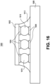
- Figure 16 illustrates a cross-sectional view of a flip-chip mounted die, in accordance with an embodiment of the present disclosure.
- an apparatus 1600 includes a die 1602 such as an integrated circuit (IC) fabricated according to one or more processes described herein or including one or more features described herein, in accordance with an embodiment of the present disclosure.
- the die 1602 includes metallized pads 1604 thereon.
- the die 1602 and package substrate 1606 are electrically connected by solder balls 1610 coupled to the metallized pads 1604 and the connections 1608.
- An underfill material 1612 surrounds the solder balls 1610.
- Processing a flip chip may be similar to conventional IC fabrication, with a few additional operations. Near the end of the manufacturing process, the attachment pads are metalized to make them more receptive to solder. This typically consists of several treatments. A small dot of solder is then deposited on each metalized pad. The chips are then cut out of the wafer as normal. To attach the flip chip into a circuit, the chip is inverted to bring the solder dots down onto connectors on the underlying electronics or circuit board. The solder is then re-melted to produce an electrical connection, typically using an ultrasonic or alternatively reflow solder process. This also leaves a small space between the chip's circuitry and the underlying mounting. In most cases an electrically-insulating adhesive is then "underfilled” to provide a stronger mechanical connection, provide a heat bridge, and to ensure the solder joints are not stressed due to differential heating of the chip and the rest of the system.
- newer packaging and die-to-die interconnect approaches such as through silicon via (TSV) and silicon interposer, are implemented to fabricate high performance Multi-Chip Module (MCM) and System in Package (SiP) incorporating an integrated circuit (IC) fabricated according to one or more processes described herein or including one or more features described herein, in accordance with an embodiment of the present disclosure.
- TSV through silicon via
- SiP System in Package
- An integrated circuit structure includes a plurality of horizontally stacked nanowires.
- a gate stack is over the plurality of horizontally stacked nanowires.
- a first epitaxial source or drain structure is at a first end of the plurality of horizontally stacked nanowires.
- a first gate spacer laterally between the gate stack and the first epitaxial source or drain structure.
- a second epitaxial source or drain structure is at a second end of the plurality of horizontally stacked nanowires.
- a second gate spacer is laterally between the gate stack and the first epitaxial source or drain structure.
- the first gate spacer has a width less than the second gate spacer.
- Example embodiment 2 The integrated circuit structure of example embodiment 1, wherein the first epitaxial source or drain structure is an epitaxial source structure, and the second epitaxial source or drain structure is an epitaxial drain structure.
- Example embodiment 3 The integrated circuit structure of example embodiment 1 or 2, further comprising a first conductive contact on a gate electrode of the gate stack, a second conductive contact on the first epitaxial source or drain structure, and a third conductive contact on the second epitaxial source or drain structure.
- Example embodiment 4 The integrated circuit structure of example embodiment 3, wherein the first conductive contact and the third conductive contact are front side contacts, and the second conductive contact is a backside contact.
- An integrated circuit structure includes a plurality of horizontally stacked nanowires.
- a gate stack is over the plurality of horizontally stacked nanowires.
- a first epitaxial source or drain structure is at a first end of the plurality of horizontally stacked nanowires.
- a first gate spacer laterally between the gate stack and the first epitaxial source or drain structure.
- a second epitaxial source or drain structure is at a second end of the plurality of horizontally stacked nanowires.
- a second gate spacer is laterally between the gate stack and the first epitaxial source or drain structure.
- the first epitaxial source or drain structure has tips having a greater lateral width than tips of the second epitaxial source or drain structure.
Landscapes
- Insulated Gate Type Field-Effect Transistor (AREA)
Applications Claiming Priority (1)
| Application Number | Priority Date | Filing Date | Title |
|---|---|---|---|
| US18/400,001 US20250220978A1 (en) | 2023-12-29 | 2023-12-29 | Integrated circuit structure with asymmetric epitaxial source or drain arrangements |
Publications (1)
| Publication Number | Publication Date |
|---|---|
| EP4580332A1 true EP4580332A1 (de) | 2025-07-02 |
Family
ID=93213558
Family Applications (1)
| Application Number | Title | Priority Date | Filing Date |
|---|---|---|---|
| EP24207744.4A Pending EP4580332A1 (de) | 2023-12-29 | 2024-10-21 | Integrierte schaltungsstruktur mit asymmetrischen epitaktischen source- oder drain-, sowie spacer- anordnungen |
Country Status (2)
| Country | Link |
|---|---|
| US (1) | US20250220978A1 (de) |
| EP (1) | EP4580332A1 (de) |
Citations (6)
| Publication number | Priority date | Publication date | Assignee | Title |
|---|---|---|---|---|
| EP3629382A1 (de) * | 2018-09-28 | 2020-04-01 | INTEL Corporation | Integrierte schaltungsstrukturen mit asymmetrischen quellen- und drain-strukturen |
| US11239359B2 (en) * | 2018-09-29 | 2022-02-01 | International Business Machines Corporation | Fabricating a gate-all-around (GAA) field effect transistor having threshold voltage asymmetry by thinning source side lateral end portion of the nanosheet layer |
| DE102021109107A1 (de) * | 2020-11-12 | 2022-05-12 | Taiwan Semiconductor Manufacturing Co., Ltd. | Gatestrukturen und verfahren zu deren ausbildung |
| US20230027676A1 (en) * | 2021-07-22 | 2023-01-26 | Taiwan Semiconductor Manufacturing Co., Ltd. | Semiconductor Devices with Uniform Gate Regions |
| US11735628B2 (en) * | 2021-03-01 | 2023-08-22 | International Business Machines Corporation | Nanosheet metal-oxide semiconductor field effect transistor with asymmetric threshold voltage |
| EP4270484A2 (de) * | 2022-03-11 | 2023-11-01 | INTEL Corporation | Integrierte schaltungsstrukturen mit selbstjustiertem rückseitenkontakt zwischen einer leitfähigen quelle und einem drain |
-
2023
- 2023-12-29 US US18/400,001 patent/US20250220978A1/en active Pending
-
2024
- 2024-10-21 EP EP24207744.4A patent/EP4580332A1/de active Pending
Patent Citations (6)
| Publication number | Priority date | Publication date | Assignee | Title |
|---|---|---|---|---|
| EP3629382A1 (de) * | 2018-09-28 | 2020-04-01 | INTEL Corporation | Integrierte schaltungsstrukturen mit asymmetrischen quellen- und drain-strukturen |
| US11239359B2 (en) * | 2018-09-29 | 2022-02-01 | International Business Machines Corporation | Fabricating a gate-all-around (GAA) field effect transistor having threshold voltage asymmetry by thinning source side lateral end portion of the nanosheet layer |
| DE102021109107A1 (de) * | 2020-11-12 | 2022-05-12 | Taiwan Semiconductor Manufacturing Co., Ltd. | Gatestrukturen und verfahren zu deren ausbildung |
| US11735628B2 (en) * | 2021-03-01 | 2023-08-22 | International Business Machines Corporation | Nanosheet metal-oxide semiconductor field effect transistor with asymmetric threshold voltage |
| US20230027676A1 (en) * | 2021-07-22 | 2023-01-26 | Taiwan Semiconductor Manufacturing Co., Ltd. | Semiconductor Devices with Uniform Gate Regions |
| EP4270484A2 (de) * | 2022-03-11 | 2023-11-01 | INTEL Corporation | Integrierte schaltungsstrukturen mit selbstjustiertem rückseitenkontakt zwischen einer leitfähigen quelle und einem drain |
Also Published As
| Publication number | Publication date |
|---|---|
| US20250220978A1 (en) | 2025-07-03 |
Similar Documents
| Publication | Publication Date | Title |
|---|---|---|
| US20230207465A1 (en) | Integrated circuit structure with buried power rail | |
| US20250227968A1 (en) | Integrated circuit structure with backside power delivery | |
| EP4485520A1 (de) | Integrierte schaltungsstruktur mit differenziertem zugriff auf die rückseite von source- oder drainkontakt | |
| US20250151344A1 (en) | Integrated circuit structure with varied internal spacers and epitaxial source or drain structures | |
| EP4300558A1 (de) | Integrierte schaltungsstruktur mit eingelassener selbstausgerichteter tiefer grenzdurchkontaktierung | |
| EP4608090A1 (de) | Integrierte schaltungsstruktur mit direktem rückseiten-source- oder drain-kontakt, der durch silicium-germanium-ätzstopp aktiviert wird | |
| EP4580345A1 (de) | Integrierte schaltungsstruktur mit vorderseitig geschnittenem rückseiten-source- oder drainkontakt | |
| NL2036460B1 (en) | Integrated circuit structure with backside source or drain contact selectivity | |
| US20250107183A1 (en) | Integrated circuit structure with differentiated source or drain structures | |
| EP4471840A1 (de) | Integrierte schaltungsstruktur mit rückseitigem kontaktheften | |
| EP4443515A1 (de) | Integrierte schaltungsstruktur mit rückseitiger kontakterweiterung | |
| EP4478421A1 (de) | Integrierte schaltungsstruktur mit gleichförmigkeit der rückseitigen kontaktanzeige | |
| US20240332377A1 (en) | Integrated circuit structure with backside source or drain contact selectivity | |
| US20240313096A1 (en) | Integrated circuit structure with back-side contact selectivity | |
| US20240429125A1 (en) | Integrated circuit structure with deep via bar isolation | |
| EP4580332A1 (de) | Integrierte schaltungsstruktur mit asymmetrischen epitaktischen source- oder drain-, sowie spacer- anordnungen | |
| EP4580343A1 (de) | Integrierte schaltungsstruktur mit direktem rückseitigen source- oder drain-kontakt | |
| EP4579740A1 (de) | Integrierte schaltungsstruktur mit rückseitenkontakterweiterung | |
| EP4580342A1 (de) | Integrierte schaltungsstruktur mit unterschiedlichen epitaktischen source- oder drain-strukturen und bauelementetypen | |
| EP4580344A1 (de) | Integrierte schaltungsstruktur mit vorderseitig geführtem rückseiten-source- oder drain-kontakt | |
| EP4626178A1 (de) | Integrierte schaltungsstruktur mit geweitetem rückseiten-source- oder drain-kontakt, der die benachbarten gates nicht überlappt | |
| US20250393251A1 (en) | Integrated circuit structure with backside conductive feed-through | |
| US20250151379A1 (en) | Integrated circuit structure with varied etch-stop for epitaxial source or drain structures | |
| US20250393245A1 (en) | Integrated circuit structure with spacer-guided backside conductive contact | |
| US20250204029A1 (en) | Integrated circuit structure with varied sub-fin trenches and epitaxial source or drain structures |
Legal Events
| Date | Code | Title | Description |
|---|---|---|---|
| PUAI | Public reference made under article 153(3) epc to a published international application that has entered the european phase |
Free format text: ORIGINAL CODE: 0009012 |
|
| STAA | Information on the status of an ep patent application or granted ep patent |
Free format text: STATUS: THE APPLICATION HAS BEEN PUBLISHED |
|
| AK | Designated contracting states |
Kind code of ref document: A1 Designated state(s): AL AT BE BG CH CY CZ DE DK EE ES FI FR GB GR HR HU IE IS IT LI LT LU LV MC ME MK MT NL NO PL PT RO RS SE SI SK SM TR |
|
| STAA | Information on the status of an ep patent application or granted ep patent |
Free format text: STATUS: REQUEST FOR EXAMINATION WAS MADE |
|
| 17P | Request for examination filed |
Effective date: 20251218 |