EP4579751A1 - Solid-state imaging device - Google Patents
Solid-state imaging device Download PDFInfo
- Publication number
- EP4579751A1 EP4579751A1 EP23857183.0A EP23857183A EP4579751A1 EP 4579751 A1 EP4579751 A1 EP 4579751A1 EP 23857183 A EP23857183 A EP 23857183A EP 4579751 A1 EP4579751 A1 EP 4579751A1
- Authority
- EP
- European Patent Office
- Prior art keywords
- capacitive element
- wiring
- state imaging
- solid
- mim
- Prior art date
- Legal status (The legal status is an assumption and is not a legal conclusion. Google has not performed a legal analysis and makes no representation as to the accuracy of the status listed.)
- Pending
Links
Images









Classifications
-
- H—ELECTRICITY
- H04—ELECTRIC COMMUNICATION TECHNIQUE
- H04N—PICTORIAL COMMUNICATION, e.g. TELEVISION
- H04N25/00—Circuitry of solid-state image sensors [SSIS]; Control thereof
- H04N25/70—SSIS architectures; Circuits associated therewith
- H04N25/76—Addressed sensors, e.g. MOS or CMOS sensors
- H04N25/77—Pixel circuitry, e.g. memories, A/D converters, pixel amplifiers, shared circuits or shared components
- H04N25/771—Pixel circuitry, e.g. memories, A/D converters, pixel amplifiers, shared circuits or shared components comprising storage means other than floating diffusion
-
- H—ELECTRICITY
- H04—ELECTRIC COMMUNICATION TECHNIQUE
- H04N—PICTORIAL COMMUNICATION, e.g. TELEVISION
- H04N25/00—Circuitry of solid-state image sensors [SSIS]; Control thereof
- H04N25/50—Control of the SSIS exposure
- H04N25/57—Control of the dynamic range
- H04N25/59—Control of the dynamic range by controlling the amount of charge storable in the pixel, e.g. modification of the charge conversion ratio of the floating node capacitance
-
- H—ELECTRICITY
- H10—SEMICONDUCTOR DEVICES; ELECTRIC SOLID-STATE DEVICES NOT OTHERWISE PROVIDED FOR
- H10F—INORGANIC SEMICONDUCTOR DEVICES SENSITIVE TO INFRARED RADIATION, LIGHT, ELECTROMAGNETIC RADIATION OF SHORTER WAVELENGTH OR CORPUSCULAR RADIATION
- H10F39/00—Integrated devices, or assemblies of multiple devices, comprising at least one element covered by group H10F30/00, e.g. radiation detectors comprising photodiode arrays
- H10F39/10—Integrated devices
- H10F39/12—Image sensors
- H10F39/18—Complementary metal-oxide-semiconductor [CMOS] image sensors; Photodiode array image sensors
-
- H—ELECTRICITY
- H10—SEMICONDUCTOR DEVICES; ELECTRIC SOLID-STATE DEVICES NOT OTHERWISE PROVIDED FOR
- H10F—INORGANIC SEMICONDUCTOR DEVICES SENSITIVE TO INFRARED RADIATION, LIGHT, ELECTROMAGNETIC RADIATION OF SHORTER WAVELENGTH OR CORPUSCULAR RADIATION
- H10F39/00—Integrated devices, or assemblies of multiple devices, comprising at least one element covered by group H10F30/00, e.g. radiation detectors comprising photodiode arrays
- H10F39/80—Constructional details of image sensors
- H10F39/803—Pixels having integrated switching, control, storage or amplification elements
-
- H—ELECTRICITY
- H10—SEMICONDUCTOR DEVICES; ELECTRIC SOLID-STATE DEVICES NOT OTHERWISE PROVIDED FOR
- H10F—INORGANIC SEMICONDUCTOR DEVICES SENSITIVE TO INFRARED RADIATION, LIGHT, ELECTROMAGNETIC RADIATION OF SHORTER WAVELENGTH OR CORPUSCULAR RADIATION
- H10F39/00—Integrated devices, or assemblies of multiple devices, comprising at least one element covered by group H10F30/00, e.g. radiation detectors comprising photodiode arrays
- H10F39/80—Constructional details of image sensors
- H10F39/803—Pixels having integrated switching, control, storage or amplification elements
- H10F39/8037—Pixels having integrated switching, control, storage or amplification elements the integrated elements comprising a transistor
-
- H—ELECTRICITY
- H10—SEMICONDUCTOR DEVICES; ELECTRIC SOLID-STATE DEVICES NOT OTHERWISE PROVIDED FOR
- H10F—INORGANIC SEMICONDUCTOR DEVICES SENSITIVE TO INFRARED RADIATION, LIGHT, ELECTROMAGNETIC RADIATION OF SHORTER WAVELENGTH OR CORPUSCULAR RADIATION
- H10F39/00—Integrated devices, or assemblies of multiple devices, comprising at least one element covered by group H10F30/00, e.g. radiation detectors comprising photodiode arrays
- H10F39/80—Constructional details of image sensors
- H10F39/809—Constructional details of image sensors of hybrid image sensors
-
- H—ELECTRICITY
- H10—SEMICONDUCTOR DEVICES; ELECTRIC SOLID-STATE DEVICES NOT OTHERWISE PROVIDED FOR
- H10F—INORGANIC SEMICONDUCTOR DEVICES SENSITIVE TO INFRARED RADIATION, LIGHT, ELECTROMAGNETIC RADIATION OF SHORTER WAVELENGTH OR CORPUSCULAR RADIATION
- H10F39/00—Integrated devices, or assemblies of multiple devices, comprising at least one element covered by group H10F30/00, e.g. radiation detectors comprising photodiode arrays
- H10F39/80—Constructional details of image sensors
- H10F39/811—Interconnections
-
- H—ELECTRICITY
- H10—SEMICONDUCTOR DEVICES; ELECTRIC SOLID-STATE DEVICES NOT OTHERWISE PROVIDED FOR
- H10F—INORGANIC SEMICONDUCTOR DEVICES SENSITIVE TO INFRARED RADIATION, LIGHT, ELECTROMAGNETIC RADIATION OF SHORTER WAVELENGTH OR CORPUSCULAR RADIATION
- H10F39/00—Integrated devices, or assemblies of multiple devices, comprising at least one element covered by group H10F30/00, e.g. radiation detectors comprising photodiode arrays
- H10F39/10—Integrated devices
- H10F39/12—Image sensors
- H10F39/199—Back-illuminated image sensors
Definitions
- a structure of a pixel of an image sensor there is known a structure that is provided with a storage capacitance that stores charges having overflown from a photodiode (see, for example, PTL 1 and PTL 2).
- the storage capacitances are disposed as a two-stage structure in the structure disclosed in PTL 2 to achieve a wider dynamic range while keeping the SN ratio, two storage capacitances are disposed on the same plane as that of the photodiode, and therefore an area of a plane on a light incidence surface side of the photodiode is limited. Hence, a technique for achieving desired characteristics with a more appropriate layout is demanded.
- a solid-state imaging device includes: a plurality of pixels that each include a photoelectric conversion element and a plurality of wiring capacitive elements; and a read-out unit that reads out signals from the plurality of pixels, the solid-state imaging device has a structure that a charge having overflown from the photoelectric conversion element is stored in a first wiring capacitive element, and the charge having overflown from the first wiring capacitive element is stored in a second wiring capacitive element, and the read-out unit individually reads out a signal of each of the photoelectric conversion element, the first wiring capacitive element, and the second wiring capacitive element.
- the solid-state imaging device has the structure that the charge having overflown from the photoelectric conversion element is stored in the first wiring capacitive element, and the charge having overflown from the first wiring capacitive element is stored in the second wiring capacitive element, and individually reads out the signal of each of the photoelectric conversion element, the first wiring capacitive element, and the second wiring capacitive element.
- a solid-state imaging device includes: a plurality of pixels that each include a plurality of photoelectric conversion elements and a plurality of wiring capacitive elements; and a read-out unit that reads out signals from the plurality of pixels, the solid-state imaging device has a structure that a first wiring capacitive element and a second wiring capacitive element are respectively connected to floating diffusions of a first photoelectric conversion element and a second photoelectric conversion element, and a charge having overflown from the first photoelectric conversion element is stored in the first wiring capacitive element, and the charge having overflown from the second photoelectric conversion element is stored in the second wiring capacitive element, and the read-out unit individually reads out a signal of each of the first photoelectric conversion element, the second photoelectric conversion element, the first wiring capacitive element, and the second wiring capacitive element.
- the solid-state imaging device has the structure that the charge having overflown from the first photoelectric conversion element is stored in the first wiring capacitive element, and the charge having overflown from the second photoelectric conversion element is stored in the second wiring capacitive element, and individually reads out the signal of each of the first photoelectric conversion element, the second photoelectric conversion element, the first wiring capacitive element, and the second wiring capacitive element.
- solid-state imaging device may be an independent device or may be an internal block constituting one device.
- Fig. 1 is a diagram illustrating a configuration example of one embodiment of a solid-state imaging device to which the present disclosure is applied.
- a solid-state imaging device 10 is a Complementary Metal Oxide Semiconductor (CMOS) type solid-state imaging device.
- the solid-state imaging device 10 includes a pixel array unit 21, a vertical drive unit 22, a column signal processing unit 23, a horizontal drive unit 24, an output unit 25, and a control unit 26.
- CMOS Complementary Metal Oxide Semiconductor
- the pixel array unit 21 includes a plurality of pixels 100 two-dimensionally aligned in a matrix on a semiconductor substrate made of silicon (Si) or the like.
- the pixel 100 includes a photodiode, a plurality of pixel transistors, and the like.
- a pixel drive line 41 is formed per row and connected to the vertical drive unit 22, and a vertical signal line 42 is formed per column and is connected to the column signal processing unit 23 for the plurality of pixels 100 two-dimensionally aligned in the matrix.
- the solid-state imaging device 10 has the multistage structure (two-stage structure) that the MIM capacitive element 131 and the MIM capacitive element 132 having the different capacitances are disposed per pixel 100, and charges having overflown from the photodiode 111 are stored in the MIM capacitive element 131 and the MIM capacitive element 132, and signals obtained from the charges stored in the photodiode 111, the MIM capacitive element 131, and the MIM capacitive element 132 are individually read out.
- the MIM capacitive element 131 and the MIM capacitive element 132 are wiring capacitive elements, and are disposed between wiring layers, so that the MIM capacitive element 131 and the MIM capacitive element 132 are not disposed on the same plane as that of the photodiode 111, and do not limit the area of the photodiode 111 (the area of the plane on the light incidence surface side). Furthermore, the photodiode 111, the MIM capacitive element 131, and the MIM capacitive element 132 are not disposed on the same plane, so that there is also an advantage for miniaturization of pixels.
- the pixel 100 has the first structure ( Fig. 2 and the other figures), so that the photodiode 111 and the MIM capacitive elements 131 and 132 are not disposed on the same plane, and it is possible to achieve both of suppression of deterioration of the SN ratio and expansion of the dynamic range. That is, it is possible to achieve desired characteristics with a more appropriate layout.
- Fig. 9 is a cross-sectional view illustrating a second example of a structure of a pixel.
- the MIM capacitive element 131 and the MIM capacitive element 132 are disposed at the same position in the Z direction, and are disposed between the same wiring layers. That is, in the wiring layer 12, both of the MIM capacitive element 131 and the MIM capacitive element 132 are disposed between the first wiring layers.
- Fig. 12 is a timing chart for describing an example of a read-out operation of the circuit configuration in Fig. 11 .
- the common control signal VMID for the MIM capacitive elements 131 and 132 are changed to the control signal VMID1 for the MIM capacitive element 131, and the control signal VMID2 for the MIM capacitive element 132. Consequently, the MIM capacitive element 131 and the MIM capacitive element 132 are individually controlled. Since a timing of a drive signal such as SEL in Fig. 12 is similar to that in Fig. 6 , description thereof will be omitted.
- FIG. 11 illustrates the example of the TG type circuit configuration
- the OFG type circuit configuration can also adopt the same configuration.
- Fig. 13 is a diagram illustrating another example of the OFG type circuit configuration illustrated in Fig. 7 .
- the upper electrode of the MIM capacitive element 131 is connected to the control power supply VMID 1
- the upper electrode of the MIM capacitive element 132 is connected to the control power supply VMID2, so that it is possible to individually control the MIM capacitive element 131 and the MIM capacitive element 132.
- Light incidence surface sides of the photodiode 211-1 and the photodiode 211-2 are provided with a color filter 201 and an on-chip microlens 202. As illustrated in the plan view of Fig. 15 , three on-chip microlenses 202-1-1 to 202-1-3 are provided to meet the L-shaped region of the photodiode 211-1, and one on-chip microlens 202-2 is provided to meet the rectangular region of the photodiode 211-2.
- the wiring layer 12 is a multilayer wiring layer that includes a plurality of wiring layers obtained by being stacked at a plurality of stages and forming a wiring 222 in each stage with an inter-wiring film 221 interposed therebetween.
- an MIM capacitive element 231 and an MIM capacitive element 232 are disposed as wiring capacitive elements having different capacitances.
- the MIM capacitive element 231 and the MIM capacitive element 232 are provided per pixel 100.
- the MIM capacitive element 231 and the MIM capacitive element 232 are disposed between different wiring layers.
- the MIM capacitive element 231 and the MIM capacitive element 232 can have the three-dimensional structures similar to the structure illustrated in Fig. 3 .
- the MIM capacitive element 231 and the MIM capacitive element 232 can have the structures whose at least ones of the film types, the thicknesses, and the areas of the dielectrics are different.
- the capacitance of the MIM capacitive element 232 is larger than the capacitance of the MIM capacitive element 231.
- Fig. 16 is a diagram illustrating an example of the circuit configuration of the pixel 100 in Fig. 14 .
- the pixel 100 includes the photodiodes 211-1 and 211-2, the MIM capacitive elements 231 and 232, a transfer transistor 261, an FD 262, a switch transistor 263, a reset transistor 264, an amplifier transistor 265, a selection transistor 266, a switch transistor 267, a storage transistor 268, and an FD 269.
- the transfer transistor 261 is provided between the photodiode 211-1 and the FD 262, and transfers the charge stored in the photodiode 211-1 to the FD 262 according to the drive signal TGL to be applied to a gate voltage of the transfer transistor 261.
- the FD 262 is a floating diffusion that converts the charge from the photodiode 211-1 into a voltage signal.
- the FD 262 is connected with the vertical signal line 42 via the amplifier transistor 265 and the selection transistor 266.
- the switch transistor 263 switches a connection state between the FD 262, the switch transistor 267, and the storage transistor 268 according to the drive signal FDG to be applied to a gate voltage of the switch transistor 263.
- the switch transistor 267 switches a connection state between the switch transistor 263, the MIM capacitive element 231, and the reset transistor 264 according to the drive signal LCG to be applied to a gate voltage of the switch transistor 267.
- the storage transistor 268 switches a connection state between the switch transistor 263 and the FD 269 according to the drive signal FCG to be applied to a gate electrode of the storage transistor 268.
- VMID represents a common control signal of the MIM capacitive elements 231 and 232 in the circuit diagram in Fig. 16 .
- SEL, FDG, TGL, RST, LCG, and FCG represent drive signals to be applied to the gate electrode of each transistor in the circuit diagram in Fig. 16 .
- the cross-sectional view of Fig. 14 illustrates the case where the MIM capacitive element 231 and the MIM capacitive element 232 are disposed between the different wiring layers
- the MIM capacitive element 231 and the MIM capacitive element 232 may be disposed between the same wiring layers.
- the inter-pixel isolation part 212 is formed as the trench formed penetrating the surface on the side opposite to the light incidence surface in the cross-sectional view of Fig. 14
- the solid-state imaging device 10 has been described as a CMOS type solid-state imaging device in the above description, and the CMOS type solid-state imaging device can have a back-illuminated structure in which light is incident from the upper layer (back surface side) located on the side opposite to the wiring layer side (front surface side) formed in the lower layer when viewed from the semiconductor substrate in which the photodiode 111 is formed as the photoelectric conversion unit.
- the CMOS type solid-state imaging device may have a front-illuminated structure in which the side on which light is incident is the wiring layer side (front surface side).
- the solid-state imaging device 10 is an example of the light detection device to which the present disclosure is applied. That is, the light detection device to which the present disclosure is applied is not limited to the solid-state imaging device 10, and is applicable to, for example, a device that detects light such as a distance measurement sensor that uses an IR laser. Note that the configuration to which the present disclosure is applied is not limited to the CMOS type solid-state imaging device, and is also applicable to other solid-state imaging devices such as the Charge Coupled Device (CCD) type.
- CCD Charge Coupled Device
- the solid-state imaging device to which the present disclosure is applied can be installed in an electronic device such as a smartphone, a tablet terminal, a mobile phone, a digital still camera, and a digital video camera.
- Fig. 19 is a block diagram illustrating a configuration example of an electronic device including the built-in solid-state imaging device to which the present disclosure is applied.
- the CPU 1010 controls an operation of each unit of the electronic device 1000.
- the optical system 1011 captures incident light (image light) from a subject and forms an image on a light detection surface of the solid-state imaging device 1012.
- the solid-state imaging device 1012 converts the light amount of incident light, with which an image is formed on the light detection surface by the optical system 1011, into an electrical signal in units of pixels, and outputs the electrical signal as a signal.
- the DSP 1013 performs predetermined signal processing on the signal output from the solid-state imaging device 1012.
- the frame memory 1014 temporarily records image data of a still image or a video captured by the imaging system.
- the display 1015 is a liquid crystal display or an organic EL display, and displays a still image or a video captured by the imaging system.
- the operation system 1016 issues an operation command for various functions of the electronic device 1000 in response to a user operation.
Landscapes
- Engineering & Computer Science (AREA)
- Multimedia (AREA)
- Signal Processing (AREA)
- Solid State Image Pick-Up Elements (AREA)
- Transforming Light Signals Into Electric Signals (AREA)
Abstract
Description
- The present disclosure relates to a solid-state imaging device and, more particularly, relates to a solid-state imaging device that achieves desired characteristics with a more appropriate layout.
- As a structure of a pixel of an image sensor, there is known a structure that is provided with a storage capacitance that stores charges having overflown from a photodiode (see, for example, PTL 1 and PTL 2).
- PTL 1 discloses a structure of a pixel that is provided with a capacitance including a cylinder type capacitor as the storage capacitance that stores charges having overflown from the photodiode. PTL 2 discloses a structure of a pixel that is provided with a first storage capacitance and a second storage capacitance that store charges having overflown from photodiodes on the same plane as that of the photodiode.
-
- [PTL 1]
JP 2020-129795A - [PTL 2]
JP 2006-245522A - Although the storage capacitance is disposed as a one-storage structure in the structure disclosed in PTL 1, it is concerned that increasing an intra-pixel capacitance to expand a dynamic range lowers conversion efficiency, and therefore random noise deteriorates. Therefore, it is necessary to limit the intra-pixel capacitance to make an SN ratio a certain criterion or more, and it is difficult to balance between the intra-pixel capacitance and the dynamic range.
- On the other hand, the storage capacitances are disposed as a two-stage structure in the structure disclosed in PTL 2 to achieve a wider dynamic range while keeping the SN ratio, two storage capacitances are disposed on the same plane as that of the photodiode, and therefore an area of a plane on a light incidence surface side of the photodiode is limited. Hence, a technique for achieving desired characteristics with a more appropriate layout is demanded.
- With such circumstances in view, the present disclosure achieves desired characteristics with a more appropriate layout.
- A solid-state imaging device according to a first aspect of the present disclosure includes: a plurality of pixels that each include a photoelectric conversion element and a plurality of wiring capacitive elements; and a read-out unit that reads out signals from the plurality of pixels, the solid-state imaging device has a structure that a charge having overflown from the photoelectric conversion element is stored in a first wiring capacitive element, and the charge having overflown from the first wiring capacitive element is stored in a second wiring capacitive element, and the read-out unit individually reads out a signal of each of the photoelectric conversion element, the first wiring capacitive element, and the second wiring capacitive element.
- The solid-state imaging device according to the first aspect of the present disclosure has the structure that the charge having overflown from the photoelectric conversion element is stored in the first wiring capacitive element, and the charge having overflown from the first wiring capacitive element is stored in the second wiring capacitive element, and individually reads out the signal of each of the photoelectric conversion element, the first wiring capacitive element, and the second wiring capacitive element.
- A solid-state imaging device according to a second aspect of the present disclosure includes: a plurality of pixels that each include a plurality of photoelectric conversion elements and a plurality of wiring capacitive elements; and a read-out unit that reads out signals from the plurality of pixels, the solid-state imaging device has a structure that a first wiring capacitive element and a second wiring capacitive element are respectively connected to floating diffusions of a first photoelectric conversion element and a second photoelectric conversion element, and a charge having overflown from the first photoelectric conversion element is stored in the first wiring capacitive element, and the charge having overflown from the second photoelectric conversion element is stored in the second wiring capacitive element, and the read-out unit individually reads out a signal of each of the first photoelectric conversion element, the second photoelectric conversion element, the first wiring capacitive element, and the second wiring capacitive element.
- The solid-state imaging device according to the second aspect of the present disclosure has the structure that the charge having overflown from the first photoelectric conversion element is stored in the first wiring capacitive element, and the charge having overflown from the second photoelectric conversion element is stored in the second wiring capacitive element, and individually reads out the signal of each of the first photoelectric conversion element, the second photoelectric conversion element, the first wiring capacitive element, and the second wiring capacitive element.
- Note that the solid-state imaging device according to one aspect of the present disclosure may be an independent device or may be an internal block constituting one device.
-
- [
Fig. 1 ]
Fig. 1 is a diagram illustrating a configuration example of one embodiment of a solid-state imaging device to which the present disclosure is applied. - [
Fig. 2 ]
Fig. 2 is a cross-sectional view illustrating a first example of a structure of a pixel. - [
Fig. 3 ]
Fig. 3 is a cross-sectional view illustrating an example of a structure of an MIM capacitive element. - [
Fig. 4 ]
Fig. 4 is a diagram illustrating a first example of a TG type circuit configuration of a pixel. - [
Fig. 5 ]
Fig. 5 is a plan view corresponding to the TG type circuit configuration of the pixel inFig. 4 . - [
Fig. 6 ]
Fig. 6 is a timing chart illustrating an example of a read-out operation of the circuit configuration of the pixel inFig. 4 . - [
Fig. 7 ]
Fig. 7 is a diagram illustrating a first example of an OFG type circuit configuration of a pixel. - [
Fig. 8 ]
Fig. 8 is a plan view corresponding to the OFG type circuit configuration of the pixel inFig. 7 . - [
Fig. 9 ]
Fig. 9 is a cross-sectional view illustrating a second example of the structure of the pixel. - [
Fig. 10 ]
Fig. 10 is a cross-sectional view illustrating a third example of the structure of the pixel. - [
Fig. 11 ]
Fig. 11 is a diagram illustrating a second example of the TG type circuit configuration of the pixel. - [
Fig. 12 ]
Fig. 12 is a timing chart illustrating an example of a read-out operation of the circuit configuration of the pixel inFig. 11 . - [
Fig. 13 ]
Fig. 13 is a diagram illustrating a second example of the OFG type circuit configuration of the pixel. - [
Fig. 14 ]
Fig. 14 is a cross-sectional view illustrating another example of the structure of the pixel. - [
Fig. 15 ]
Fig. 15 is a plan view corresponding to the pixel inFig. 14 . - [
Fig. 16 ]
Fig. 16 is a diagram illustrating an example of the circuit configuration of the pixel inFig. 14 . - [
Fig. 17 ]
Fig. 17 is a timing chart illustrating an example of a read-out operation of the circuit configuration of the pixel inFig. 16 . - [
Fig. 18 ]
Fig. 18 is a cross-sectional view illustrating another example of a structure of an MIM capacitive element. - [
Fig. 19 ]
Fig. 19 is a block diagram illustrating a configuration example of an electronic device including the built-in solid-state imaging device to which the present disclosure is applied. -
Fig. 1 is a diagram illustrating a configuration example of one embodiment of a solid-state imaging device to which the present disclosure is applied. - In
Fig. 1 , a solid-state imaging device 10 is a Complementary Metal Oxide Semiconductor (CMOS) type solid-state imaging device. The solid-state imaging device 10 includes apixel array unit 21, avertical drive unit 22, a columnsignal processing unit 23, ahorizontal drive unit 24, anoutput unit 25, and acontrol unit 26. - The
pixel array unit 21 includes a plurality ofpixels 100 two-dimensionally aligned in a matrix on a semiconductor substrate made of silicon (Si) or the like. Thepixel 100 includes a photodiode, a plurality of pixel transistors, and the like. In thepixel array unit 21, apixel drive line 41 is formed per row and connected to thevertical drive unit 22, and avertical signal line 42 is formed per column and is connected to the columnsignal processing unit 23 for the plurality ofpixels 100 two-dimensionally aligned in the matrix. - The
vertical drive unit 22 is configured as a shift register, an address decoder, or the like, and drives eachpixel 100 aligned in thepixel array unit 21. A signal output from eachpixel 100 selected and scanned by thevertical drive unit 22 is supplied to the columnsignal processing unit 23 through thevertical signal line 42. - The column
signal processing unit 23 performs predetermined signal processing (e.g. noise canceling processing or sampling processing) on the signal output from eachpixel 100 of the selected row through thevertical signal line 42 per pixel column of thepixel array unit 21, and temporarily holds the signal after the signal processing. - The
horizontal drive unit 24 is configured as a shift register, an address decoder, or the like, and sequentially selects unit circuits corresponding to the pixel columns of the columnsignal processing unit 23. By selection and scanning performed by thehorizontal drive unit 24, signals subjected to signal processing by the columnsignal processing unit 23 are output to theoutput unit 25 through thehorizontal signal line 51. - The
output unit 25 performs predetermined signal processing on the signals sequentially input from the respective columnsignal processing units 23 through thehorizontal signal line 51, and outputs the resulting signals. - The
control unit 26 includes a timing generator or the like that generates various timing signals, and controls of driving of thevertical drive unit 22, the columnsignal processing unit 23, thehorizontal drive unit 24, and the like based on the various timing signals generated by the timing generator. - Next, a first configuration to a fifth configuration will be described as configurations of the
pixels 100 two-dimensionally aligned in thepixel array unit 21, and a read-out unit that reads out the signals from the plurality ofpixels 100 in the solid-state imaging device 10. The read-out unit includes, for example, thevertical drive unit 22, the columnsignal processing unit 23, and thecontrol unit 26. -
Fig. 2 is a cross-sectional view illustrating a first example of the structure of thepixel 100. InFig. 2 , in the three directions orthogonal to each other in a space, a first direction and a second direction orthogonal to each other in the same plane are an X direction and a Y direction, respectively, and a third direction orthogonal to each of the first direction and the second direction is a Z direction. Finally, inFig. 2 , a thickness direction of each layer will be described as the Z direction. The same also applies to other figures to be described later. - Each
pixel 100 is formed by laminating asemiconductor layer 11 and awiring layer 12. Acolor filter 101 and an on-chip microlens 102 are disposed on a light incident surface side of thesemiconductor layer 11. Thecolor filter 101 and the on-chip microlens 102 are provided perpixel 100. Thecolor filter 101 is configured as a filter that allows transmission of a wavelength corresponding to, for example, one of Red (R), Green (G), and Blue (B). - A
photodiode 111 is formed on a semiconductor substrate made of silicon (Si) or the like in thesemiconductor layer 11. For example, the semiconductor substrate includes a P well layer in part of a top surface and an area near the top surface, and includes an N-type region whose conductive type is different from that of the P well layer in other regions. Thus, thephotodiode 111 is formed as a photoelectric conversion element. Eachpixel 100 is electrically and optically isolated by aninter-pixel isolation part 112. Theinter-pixel isolation part 112 is formed by burying a metal film, an insulating film, or the like in a trench formed by penetrating the semiconductor substrate from a surface on a side opposite to the light incidence surface. - The
wiring layer 12 is a multilayer wiring layer that includes plurality of wiring layers obtained by being stacked at a plurality of stages and forming awiring 122 in each stage with aninter-wiring layer film 121 interposed therebetween. Theinter-wiring layer film 121 is formed as a film for which a material such as a silicon oxide (SiO2) is used. Thewiring 122 is formed with copper (Cu) or the like. In thewiring layer 12, a Metal Insulator Metal (MIM)capacitive element 131 and anMIM capacitive element 132 are disposed as wiring capacitive elements having different capacitances between the wiring layers. - The
MIM capacitive element 131 and theMIM capacitive element 132 are provided perpixel 100. TheMIM capacitive element 131 and theMIM capacitive element 132 are disposed so that at least a part of each other overlap on a plane in an X and Y directions. Furthermore, theMIM capacitive element 132 is disposed at a position deeper than that of theMIM capacitive element 131 in the Z direction, and is disposed between different wiring layers. That is, theMIM capacitive element 131 is disposed between first wiring layers, and theMIM capacitive element 132 is disposed between second wiring layers in thewiring layer 12. - The
MIM capacitive element 131 stores charges having overflown from thephotodiode 111. TheMIM capacitive element 132 stores a charge having overflown from theMIM capacitive element 131. This structure makes it possible to store in theMIM capacitive element 131 and theMIM capacitive element 132 the charges having overflown from thephotodiode 111 together with the charges stored in thephotodiode 111, and read out the charges. -
Fig. 3 is a cross-sectional view illustrating an example of the structure of theMIM capacitive element 131. InFig. 3 , theMIM capacitive element 131 has a three-dimensional structure in the X, Y, and Z directions. TheMIM capacitive element 131 has the structure formed by laminating anupper electrode 141, alower electrode 142, and a dielectric 143 sandwiched between theupper electrode 141 and thelower electrode 142. Acap film 144 is formed on the upper surface of theupper electrode 141. Theupper electrode 141 is connected with awiring 122A via acontact 123A. Thelower electrode 142 is connected with awiring 122B. - The
upper electrode 141 is formed with a single layer film for which a material such as titanium nitride (TiN), tantalum (Ta), tantalum nitride (TaN), or tungsten nitride (WN) is used, or a laminated film formed by laminating these materials. Thelower electrode 142 is formed with a single layer film or a laminated film for which a material such as titanium nitride (TiN) is used similarly to theupper electrode 141. The dielectric 143 is formed with a single layer film for which a high permittivity material such as aluminum oxide (AlO), hafnium oxide (HfO), zirconium oxide (ZrO), or niobium oxide (NbO) is used, or a laminated film obtained by laminating these materials. Thecap film 144 is formed with a film for which a material such as silicon nitride (SiN), silicon oxide (SiO), or silicon carbonitride (SiCN) is used. - The
MIM capacitive element 132 has a similar structure to that of theMIM capacitive element 131 illustrated inFig. 3 , yet has a different film type, thickness, and area of the dielectric 143. As for the film type of the dielectric 143, the film type may be varied not only by changing the above material or but also by using a film having different characteristics even in a case of the same material. The thickness of the dielectric 143 is indicated in the Z direction, and is represented by h inFig. 3 . The area of the dielectric 143 is an area of the plane in the X and Y directions. Such a difference between the structures makes the capacitances of theMIM capacitive element 131 and theMIM capacitive element 132 different. For example, it is desirable to make the capacitance of theMIM capacitive element 132 larger than the capacitance of theMIM capacitive element 131, and make a capacitance ratio of these capacitances approximately 1:30. - As described above, although the
MIM capacitive element 131 and theMIM capacitive element 132 have the structures whose at least ones of the film types, the thicknesses, and the areas of thedielectrics 143 are different, yet the other structures may be different. For example, theMIM capacitive element 131 and theMIM capacitive element 132 may have different heights that are represented by H inFig. 3 . Furthermore, the structures of theMIM capacitive element 131 and theMIM capacitive element 132, and a manufacturing process thereof may be different. TheMIM capacitive element 131 and theMIM capacitive element 132 have the three-dimensional structures, so that it is possible to increase the capacitance per unit area, and achieve miniaturization. -
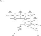
Fig. 4 is a diagram illustrating a first example of a circuit configuration of thepixel 100. InFig. 4 , thepixel 100 includes thephotodiode 111, theMIM capacitive element 131, theMIM capacitive element 132, atransfer transistor 161, anFD 162, aswitch transistor 163, areset transistor 164, anamplifier transistor 165, aselection transistor 166, afirst storage transistor 167, and asecond storage transistor 168. - The
transfer transistor 161 is provided between thephotodiode 111 and theFD 162, and transfers the charge stored in thephotodiode 111 to theFD 162 according to a drive signal TGL to be applied to a gate voltage of thetransfer transistor 161. TheFD 162 is a Floating Diffusion (FD) that converts the charge from thephotodiode 111 into a voltage signal. - The
FD 162 is connected with theswitch transistor 163 for switching conversion efficiency, and is connected with thereset transistor 164 via theswitch transistor 163. Furthermore, theFD 162 is also connected with thevertical signal line 42 via theamplifier transistor 165 and theselection transistor 166. Thefirst storage transistor 167 is connected between theswitch transistor 163 and thereset transistor 164. Thefirst storage transistor 167 is connected with theMIM capacitive element 131 and thesecond storage transistor 168. Thesecond storage transistor 168 is connected with theMIM capacitive element 132. An upper electrode of theMIM capacitive element 131 and an upper electrode of theMIM capacitive element 132 are connected with a common control power supply (VMID). - The
switch transistor 163 switches a connection state between theFD 162, and thereset transistor 164 and thefirst storage transistor 167 according to a drive signal FDG to be applied to a gate voltage of theswitch transistor 163. Thefirst storage transistor 167 switches a connection state with theMIM capacitive element 131 according to a drive signal FCG1 to be applied to a gate electrode of thefirst storage transistor 167. Thesecond storage transistor 168 switches a connection state with theMIM capacitive element 132 according to a drive signal FCG2 to be applied to a gate electrode of thesecond storage transistor 168. - In, for example, a storage period, a charge before the
photodiode 111 is saturated is stored in thephotodiode 111, and a charge at a time when thephotodiode 111 is over-saturated can be stored in theMIM capacitive element 131 via thetransfer transistor 161, theswitch transistor 163, and thefirst storage transistor 167. Furthermore, the charge at a time when thephotodiode 111 and theMIM capacitive element 131 are over-saturated can be stored in theMIM capacitive element 132 via thesecond storage transistor 168. - The
reset transistor 164 drains and resets the charges of theFD 162, theMIM capacitive element 131, and theMIM capacitive element 132 according to a drive signal RST to be applied to a gate electrode of thereset transistor 164. Theamplifier transistor 165 is an input unit of a source follower circuit that has a gate electrode connected to theFD 162 and a drain connected to a power supply voltage (VDD), and reads out the charge obtained by photoelectric conversion by thephotodiode 111. That is, theamplifier transistor 165 includes the source connected to thevertical signal line 42 via theselection transistor 166 to constitute a constant current source and the source follower circuit connected to one end of thevertical signal line 42. - The
selection transistor 166 is connected between the source of theamplifier transistor 165 and thevertical signal line 42. Theselection transistor 166 brings thepixel 100 in a selected state according to a drive signal SEL to be applied to a gate electrode of theselection transistor 166. When thepixel 100 is brought into the selected state, a signal output from theamplifier transistor 165 is read out by the columnsignal processing unit 23 via thevertical signal line 42. -
Fig. 5 is a plan view illustrating a first example of the configuration of thepixel 100. Parts corresponding to those in the circuit diagram inFig. 4 will be assigned the same reference numerals in the plan view ofFig. 5 . InFigs. 4 and5 , the charges having overflown from thephotodiode 111 are stored in theMIM capacitive element 131 and theMIM capacitive element 132 via thetransfer transistor 161 that is a transfer gate. That is, the configurations illustrated inFigs. 4 and5 are Transfer Gate (TG) type configurations. Furthermore, the configurations illustrated inFigs. 4 and5 are configurations where theFD 162 connected with theMIM capacitive element 131 and theMIM capacitive element 132 are isolated by the operation of thesecond storage transistor 168 to read out the charges respectively stored in theMIM capacitive element 131 and theMIM capacitive element 132. - Next, an example of a read-out operation of the
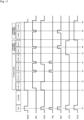
pixel 100 will be described with reference to a timing chart inFig. 6 . InFig. 6 , VMID represents a common control signal of the MIM capacitiveelements Fig. 4 . SEL, FDG, TGL, RST, FCG1, and FCG2 represent drive signals to be applied to the gate electrode of each transistor in the circuit diagram inFig. 4 . The drive signal is applied by thevertical drive unit 22 under control of thecontrol unit 26. Each transistor enters an on state when the drive signal reaches an H level, and enters an off state when the drive signal reaches an L level. - In
Fig. 6 , a storage period starts after a shutter (SHT) is released at a time t0. When the control signal VMID and the drive signals FDG, TGL, RST, FCG1, and FCG2 reach the H level before the storage period, theFD 162 and the MIM capacitiveelements photodiode 111 can be obtained (P-PD_L). Then, when the drive signal FDG reaches the L level at a time t2 in a state where the drive signal SEL continues the H level, the reset level of high conversion efficiency of thephotodiode 111 can be obtained (P-PD_H). - Next, when the drive signal SEL reaches the L level and the drive signal TGL reaches the H level at a time t3, a signal level of high conversion efficiency of the
photodiode 111 can be obtained (D-PD_H). Furthermore, when the drive signal FDG reaches the H level immediately before a time t4, and the drive signal SEL reaches the L level and the drive signal TGL reaches the H level at the time t4, the signal level of low conversion efficiency can be obtained (D-PD_L). Note that the drive signal FDG maintains the H level thereafter. - The signal level and the reset level obtained as described above are output from the
pixel 100, so that, by performing Correlated Double Sampling (CDS) based on these signal level and reset level, the columnsignal processing unit 23 can read out a signal obtained from the charge stored in the photodiode 111 (PD Read (CDS)). - Subsequently, when the drive signal FCG1 reaches the H level at a time t5, the signal level of the
MIM capacitive element 131 can be obtained (D-MIM1). The drive signal FCG1 maintains the H level at or after the time t5. Next, when the drive signal SEL reaches the L level and the drive signal FCG2 reaches the H level at a time t6, a signal level of theMIM capacitive element 132 can be obtained (D-MIM2). The drive signal FCG2 maintains the H level between the time t6 and a time t8. Next, when the drive signal RST reaches the H level at the time t7, the reset level of theMIM capacitive element 132 can be obtained (P-MIM2). When the drive signal SEL reaches the L level and the drive signal FCG2 reaches the L level at the time t8, a reset level of theMIM capacitive element 131 can be obtained (P-MIM1). - The signal level and the reset level obtained as described above are output from the
pixel 100, so that, by performing Double Data Sampling (DDS) based on these signal level and reset level, the columnsignal processing unit 23 can read out signals obtained from the charges respectively stored in theMIM capacitive element 131 and the MIM capacitive element 132 (PD+MIM1+MIM2 Read(DDS)). That is, it is possible to individually read out the charges respectively stored in thephotodiode 111, theMIM capacitive element 131, and theMIM capacitive element 132. - Although the above-described configuration has been described as the TG type configuration, other configurations may be adopted. For example, it is possible to adopt an Over Flow Gate (OFG) type configuration where an overflow path from the
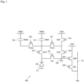
photodiode 111 is another path different from that of the transfer gate.Fig. 7 illustrates the OFG type configuration as a second example of the circuit configuration of thepixel 100. Furthermore,Fig. 8 is a plan view corresponding to the circuit configuration inFig. 7 . - In
Fig. 7 , thephotodiode 111 is connected with thetransfer transistor 161, and is connected with aconnection transistor 181 that is an overflow gate. Theconnection transistor 181 is connected to a connection point of thefirst storage transistor 167, thesecond storage transistor 168, and theMIM capacitive element 131. Theconnection transistor 181 switches a connection state between thephotodiode 111 and theMIM capacitive element 131 according to a drive signal OFG to be applied to a gate electrode of theconnection transistor 181. - Consequently, the charge before the
photodiode 111 is saturated is stored in thephotodiode 111, and the charge at a time when thephotodiode 111 is over-saturated is stored in theMIM capacitive element 131 via theconnection transistor 181. Furthermore, the charge at a time when thephotodiode 111 and theMIM capacitive element 131 are over-saturated can be stored in theMIM capacitive element 132 via theconnection transistor 181 and thesecond storage transistor 168. - Both of the TG type configuration and the OFG type configuration are configurations where the floating diffusions connected with the
MIM capacitive element 131 and theMIM capacitive element 132 are isolated by thesecond storage transistor 168, and charges stored in the respective floating diffusions are read out. The TG type configuration can be configured by reducing the number of transistors compared to the OFG type configuration. According to the OFG type configuration, a region of the floating diffusion at a time when the charges stored in theMIM capacitive element 131 and theMIM capacitive element 132 are read out, and is separated from a region of the floating diffusion at a time when the charge stored in thephotodiode 111 is read out, so that it is possible to reduce noise at the former time of reading out of the charges. - As described above, the solid-
state imaging device 10 has the multistage structure (two-stage structure) that theMIM capacitive element 131 and theMIM capacitive element 132 having the different capacitances are disposed perpixel 100, and charges having overflown from thephotodiode 111 are stored in theMIM capacitive element 131 and theMIM capacitive element 132, and signals obtained from the charges stored in thephotodiode 111, theMIM capacitive element 131, and theMIM capacitive element 132 are individually read out. Note that a read-out method only needs to individually read out signals obtained from the charges stored in thephotodiode 111, theMIM capacitive element 131, and theMIM capacitive element 132, and is not limited to the operation illustrated inFig. 6 , and other read-out methods may be used. - By the way, although, according to above-described PTL 1, a storage capacitance that stores charges having overflown from a photodiode is disposed as a one-stage structure, increasing an intra-pixel capacitance to expand a dynamic range lowers conversion efficiency in a case of the one-stage structure, and therefore random noise deteriorates in proportion to a root of the capacitance.
- That is, conversion efficiency (η) of a pixel is determined according to η[V/e-] = q[C]/Cfd[F] in proportion to an FD capacitance and becomes smaller as the capacitance becomes larger. On the other hand, a random noise component is read out by DDS in a case of the one-stage structure, and therefore circuit noise, kTC noise, and AMP noise become dominant. Here, in a case where the circuit noise is σAFE, the kTC noise is σKTC, and the AMP noise is σAMP, total random noise σtotal is a square sum of each noise. To convert the noise component into the number of electrons, the noise component is divided by conversion efficiency, and therefore σtotal/η[e-rms] holds. σKTC is inversely proportional to √2kT/C and the capacitance, and deteriorates depending on the root of the capacitance when converted into the number of electrons. Therefore, it is necessary to limit the intra-pixel capacitance to make an SN ratio a certain reference or more, and it is difficult to balance between the intra-pixel capacitance and the dynamic range.
- Furthermore, although, according to above-described PTL 2, storage capacitances that store charges having overflown from a photodiode are disposed as a two-stage structure to achieve a wider dynamic range while keeping SN ratios, a wiring capacitive element (MIM capacitive element) is not disposed as the storage capacitance in this structure. Hence, two storage capacitances are disposed on the same plane as that of the photodiode, and therefore the area of the photodiode (an area of a plane on a light incidence surface side) is limited. Furthermore, the photodiode and the two storage capacitances are disposed on the same plane, and therefore are not suitable for miniaturization of pixels, either.
- By contrast with this, the solid-
state imaging device 10 to which the present disclosure is applied has the structure that the MIM capacitive element of the two stages are disposed as storage capacitances that store charges having overflown from thephotodiode 111, so that, by sequentially reading out signals obtained from the charges stored in thephotodiode 111, theMIM capacitive element 131, and theMIM capacitive element 132, it is possible to suppress the conversion efficiency ratio to a degree (approximately 1:30) matching the capacitance ratio, and expand the dynamic range without deteriorating the SN ratios of the MIM capacitive elements. - Furthermore, the
MIM capacitive element 131 and theMIM capacitive element 132 are wiring capacitive elements, and are disposed between wiring layers, so that theMIM capacitive element 131 and theMIM capacitive element 132 are not disposed on the same plane as that of thephotodiode 111, and do not limit the area of the photodiode 111 (the area of the plane on the light incidence surface side). Furthermore, thephotodiode 111, theMIM capacitive element 131, and theMIM capacitive element 132 are not disposed on the same plane, so that there is also an advantage for miniaturization of pixels. Although, particularly in a case where the capacitance ratio of the storage capacitances of the two-stage structure is approximately 1:30, it is difficult to dispose the photodiode and the two storage capacitances on the same plane depending on pixel sizes, disposing theMIM capacitive element 131 and theMIM capacitive element 132 having the different capacitances between the wiring layers is advantageous for miniaturization. - As described above, in the solid-
state imaging device 10 to which the present disclosure is applied, thepixel 100 has the first structure (Fig. 2 and the other figures), so that thephotodiode 111 and the MIM capacitiveelements - Although the first configuration (
Fig. 2 and the other figures) has been described as a configuration where theMIM capacitive element 131 and theMIM capacitive element 132 are disposed between different wiring layers in thewiring layer 12, there may be employed a configuration where theMIM capacitive element 131 and theMIM capacitive element 132 are disposed between the same wiring layers.Fig. 9 is a cross-sectional view illustrating a second example of a structure of a pixel. InFig. 9 , in thewiring layer 12, theMIM capacitive element 131 and theMIM capacitive element 132 are disposed at the same position in the Z direction, and are disposed between the same wiring layers. That is, in thewiring layer 12, both of theMIM capacitive element 131 and theMIM capacitive element 132 are disposed between the first wiring layers. - In
Fig. 9 , theMIM capacitive element 131 and theMIM capacitive element 132 have the structures illustrated inFig. 3 , have the different film types, thicknesses, and the like of thedielectrics 143, and therefore have the different capacitances. InFig. 9 , too, the capacitance ratio of the capacitance of theMIM capacitive element 131 and the capacitance of theMIM capacitive element 132 is a desired capacitance ratio. - The second configuration can adopt the TG type or OFG type configuration as a circuit configuration thereof similarly to the above-described first configuration. Furthermore, a configuration and an operation of a read-out unit that individually reads out charges respectively stored in the
photodiode 111, theMIM capacitive element 131, and theMIM capacitive element 132 in the second configuration are the same as those of the above-described first configuration. Description of these configuration and operation is repetition, and therefore will be omitted. - Although the
inter-pixel isolation part 112 is formed as the trench formed from the surface on the side opposite to the light incidence surface in the first configuration (Fig. 2 and the other figures) and the second configuration (Fig. 9 ), there may be employed a configuration where theinter-pixel isolation part 112 is formed as a trench formed from the light incidence surface side.Fig. 10 is a cross-sectional view illustrating a third example of a structure of a pixel. InFig. 10 , theinter-pixel isolation part 113 is formed by burying a metal film, an insulating film, or the like in a trench formed at a predetermined depth from the light incidence surface side in a semiconductor substrate. - In
Fig. 10 , in thewiring layer 12, theMIM capacitive element 131 and theMIM capacitive element 132 are disposed between the different wiring layers, yet may be disposed between the same wiring layers. TheMIM capacitive element 131 and theMIM capacitive element 132 have different capacitances to achieve a desired capacitance ratio. - The third configuration can adopt the TG type or OFG type configuration as a circuit configuration thereof similarly to the above-described first configuration. Furthermore, a configuration and an operation of a read-out unit that individually reads out charges respectively stored in the
photodiode 111, theMIM capacitive element 131, and theMIM capacitive element 132 in the third configuration are also the same as those of the above-described first configuration. Description of these configuration and operation is repetition, and therefore will be omitted. - Although the first configuration (
Fig. 4 ) is the TG type circuit configuration where the common control power supply (VMID) is connected to the upper electrode of theMIM capacitive element 131 and the upper electrode of theMIM capacitive element 132 to make a control signal (VMID signal) common, theMIM capacitive element 131 and theMIM capacitive element 132 may be individually controlled.Fig. 11 is a diagram illustrating another example of the TG type circuit configuration illustrated inFig. 4 . InFig. 11 , the upper electrode of theMIM capacitive element 131 is connected to a control power supply VMID1, and the upper electrode of theMIM capacitive element 132 is connected to a control power supply VMID2. - The circuit configuration in
Fig. 11 can independently control the control signal VMID1 of theMIM capacitive element 131 and the control signal VMID2 of theMIM capacitive element 132, and individually adjust charge amounts (electron amounts) respectively stored in theMIM capacitive element 131 and theMIM capacitive element 132. Furthermore, when the voltage of the control signal VMID is increased in the storage period, saturation charges of the MIM capacitive elements increase, a dark current deteriorates, and therefore the SN ratio and the dynamic range are trade-off. Hence, in the circuit configuration inFig. 11 , by independently controlling theMIM capacitive element 131 and theMIM capacitive element 132 using the control signal VMID1 and the control signal VMID2, and enabling optimal voltage control. This makes it easy to achieve both the SN ratios of the MIM capacitive elements and the dynamic range. -
Fig. 12 is a timing chart for describing an example of a read-out operation of the circuit configuration inFig. 11 . Compared to the timing chart inFig. 6 , in the timing chart inFig. 12 , the common control signal VMID for the MIM capacitiveelements MIM capacitive element 131, and the control signal VMID2 for theMIM capacitive element 132. Consequently, theMIM capacitive element 131 and theMIM capacitive element 132 are individually controlled. Since a timing of a drive signal such as SEL inFig. 12 is similar to that inFig. 6 , description thereof will be omitted. - Note that, although
Fig. 11 illustrates the example of the TG type circuit configuration, the OFG type circuit configuration can also adopt the same configuration.Fig. 13 is a diagram illustrating another example of the OFG type circuit configuration illustrated inFig. 7 . Similarly toFig. 11 , inFig. 13 , the upper electrode of theMIM capacitive element 131 is connected to the control power supply VMID 1, and the upper electrode of theMIM capacitive element 132 is connected to the control power supply VMID2, so that it is possible to individually control theMIM capacitive element 131 and theMIM capacitive element 132. -
Fig. 14 is a cross-sectional view illustrating another example of the structure of thepixel 100. The cross-sectional view ofFig. 14 corresponds to an X-X' cross section in a plan view ofFig. 15 . - Each
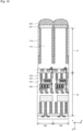
pixel 100 is formed by laminating thesemiconductor layer 11 and thewiring layer 12. In thesemiconductor layer 11, a photodiode 211-1 and a photodiode 211-2 are formed perpixel 100. As illustrated in the plan view ofFig. 15 , an L-shaped region is a region of the photodiode 211-1, and the rest of a rectangular region is a region of the photodiode 211-2 in a region of the plane in the X and Y directions (the plane on the light incidence surface side). As described above, the photodiode 211-1 has a larger area of a light reception surface than that of the photodiode 211-2, and has high sensitivity with respect to light. That is, thepixel 100 is provided with two photodiodes having different sensitivities. - Light incidence surface sides of the photodiode 211-1 and the photodiode 211-2 are provided with a
color filter 201 and an on-chip microlens 202. As illustrated in the plan view ofFig. 15 , three on-chip microlenses 202-1-1 to 202-1-3 are provided to meet the L-shaped region of the photodiode 211-1, and one on-chip microlens 202-2 is provided to meet the rectangular region of the photodiode 211-2. The shapes and the number of the on-chip microlenses 202 disposed perpixel 100 are arbitrary, and, for example, the diameters of the on-chip microlenses 202-1-1 and 202-1-3 may be made larger than the diameters of the on-chip microlenses 202-1-2 and 202-2. - The
color filter 201 is configured as, for example, a filter that allows transmission of a wavelength of the same color perpixel 100. Eachpixel 100 is isolated by theinter-pixel isolation part 212. Furthermore, in eachpixel 100, the photodiode 211-1 and the photodiode 211-2 are also isolated by theinter-pixel isolation part 212. - The
wiring layer 12 is a multilayer wiring layer that includes a plurality of wiring layers obtained by being stacked at a plurality of stages and forming awiring 222 in each stage with an inter-wiring film 221 interposed therebetween. In thewiring layer 12, anMIM capacitive element 231 and anMIM capacitive element 232 are disposed as wiring capacitive elements having different capacitances. TheMIM capacitive element 231 and theMIM capacitive element 232 are provided perpixel 100. TheMIM capacitive element 231 and theMIM capacitive element 232 are disposed between different wiring layers. TheMIM capacitive element 231 and theMIM capacitive element 232 can have the three-dimensional structures similar to the structure illustrated inFig. 3 . That is, theMIM capacitive element 231 and theMIM capacitive element 232 can have the structures whose at least ones of the film types, the thicknesses, and the areas of the dielectrics are different. For example, the capacitance of theMIM capacitive element 232 is larger than the capacitance of theMIM capacitive element 231. - The
MIM capacitive element 231 stores a charge having overflown from the photodiode 211-1. TheMIM capacitive element 232 stores a charge having overflown from the photodiode 211-2. This structure makes it possible to store in theMIM capacitive element 231 and theMIM capacitive element 232 the charges having overflown from the photodiodes 211-1 and 211-2 together with the charges stored in the photodiodes 211-1 and 212-2, and read out the charges. -
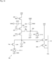
Fig. 16 is a diagram illustrating an example of the circuit configuration of thepixel 100 inFig. 14 . InFig. 16 , thepixel 100 includes the photodiodes 211-1 and 211-2, the MIM capacitiveelements transfer transistor 261, anFD 262, aswitch transistor 263, areset transistor 264, anamplifier transistor 265, aselection transistor 266, aswitch transistor 267, astorage transistor 268, and anFD 269. - The
transfer transistor 261 is provided between the photodiode 211-1 and theFD 262, and transfers the charge stored in the photodiode 211-1 to theFD 262 according to the drive signal TGL to be applied to a gate voltage of thetransfer transistor 261. TheFD 262 is a floating diffusion that converts the charge from the photodiode 211-1 into a voltage signal. TheFD 262 is connected with thevertical signal line 42 via theamplifier transistor 265 and theselection transistor 266. - The
FD 262 is connected with theswitch transistor 263 for switching conversion efficiency, and is connected with theswitch transistor 267 and thestorage transistor 268 via theswitch transistor 263. Theswitch transistor 267 is connected with theMIM capacitive element 231 and thereset transistor 264. A region including a connection point of the photodiode 211-2, theMIM capacitive element 232, and thestorage transistor 268 is theFD 269. TheFD 269 is a floating diffusion that converts the charge from the photodiode 211-2 into a voltage signal. An upper electrode of theMIM capacitive element 231 and an upper electrode of theMIM capacitive element 232 are connected with a control power supply (VMID). - The
switch transistor 263 switches a connection state between theFD 262, theswitch transistor 267, and thestorage transistor 268 according to the drive signal FDG to be applied to a gate voltage of theswitch transistor 263. Theswitch transistor 267 switches a connection state between theswitch transistor 263, theMIM capacitive element 231, and thereset transistor 264 according to the drive signal LCG to be applied to a gate voltage of theswitch transistor 267. Thestorage transistor 268 switches a connection state between theswitch transistor 263 and theFD 269 according to the drive signal FCG to be applied to a gate electrode of thestorage transistor 268. - In, for example, a storage period, a charge before the photodiode 211-1 is saturated is stored in the photodiode 211-1, and a charge at a time when the photodiode 211-1 is over-saturated can be stored in the
MIM capacitive element 231 via thetransfer transistor 261, theswitch transistor 263, and theswitch transistor 267. Furthermore, the charge of the photodiode 211-2 can be stored in theMIM capacitive element 232. - Next, an example of the read-out operation of the
pixel 100 inFig. 16 will be described with reference to a timing chart inFig. 17 . InFig. 17 , VMID represents a common control signal of the MIM capacitiveelements Fig. 16 . SEL, FDG, TGL, RST, LCG, and FCG represent drive signals to be applied to the gate electrode of each transistor in the circuit diagram inFig. 16 . - In
Fig. 17 , a storage period starts after a shutter (SHT) is released at the time t0. When the control signal VMID and the drive signals FDG, TGL, RST, LCG, and FCG reach the H level before the storage period, theFDs elements - Next, when the drive signal SEL reaches the L level and the drive signal TGL reaches the H level at the time t3, a signal level of high conversion efficiency of the photodiode 211-1 can be obtained (D-SP1_H). Furthermore, when the drive signal FDG reaches the H level immediately before the time t4, and the drive signal SEL reaches the L level and the drive signal TGL reaches the H level at the time t4, the signal level of intermediate conversion efficiency can be obtained (D-SP1_M). Note that the drive signal FDG maintains the H level thereafter.
- The signal level and the reset level obtained as described above are output from the
pixel 100, so that, by performing CDS based on these signal level and reset level, it is possible to read out a signal obtained from the charge stored in the photodiode 211-1 (PD Read (CDS)). - Subsequently, when the drive signal LCG reaches the H level immediately before the time t5, a signal level of low conversion efficiency of the photodiode 211-1 can be obtained (D-SP1_L). The drive signal LCG maintains the H level up to a time immediately before the time t7. Next, when the drive signal SEL reaches the L level and the drive signal RST reaches the H level at the time t6, a reset level of low conversion efficiency of the photodiode 211-1 can be obtained (P-SP1_L). The signal level and the reset level obtained as described above are output from the
pixel 100, so that, by performing DDS based on these signal level and reset level, it is possible to read out the charge stored in theMIM capacitive element 231 together with the charge stored in the photodiode 211-1 (PD+MIM1 Read(DDS)). - Subsequently, when the drive signal FCG reaches the H level at the time t7, a signal level of the photodiode 211-2 can be obtained (D-SP2). The drive signal FCG maintains the H level thereafter. Next, when the drive signal SEL reaches the L level and the drive signal RST reaches the H level at the time t8, a reset level of the photodiode 211-2 can be obtained (P-SP2). The signal level and the reset level obtained as described above are output from the
pixel 100, so that, by performing DDS based on these signal level and reset level, it is possible to read out the charge stored in theMIM capacitive element 232 together with the charge stored in the photodiode 211-2 (PD+MIM2 Read(DDS)). As described above, it is possible to individually read out the charges respectively stored in the photodiode 211-1, the photodiode 211-2, theMIM capacitive element 231, and theMIM capacitive element 232. - Note that, although the cross-sectional view of
Fig. 14 illustrates the case where theMIM capacitive element 231 and theMIM capacitive element 232 are disposed between the different wiring layers, theMIM capacitive element 231 and theMIM capacitive element 232 may be disposed between the same wiring layers. Furthermore, although theinter-pixel isolation part 212 is formed as the trench formed penetrating the surface on the side opposite to the light incidence surface in the cross-sectional view ofFig. 14 , there may be employed a configuration where theinter-pixel isolation part 212 is formed as a trench formed at a predetermined depth from the light incidence surface side. - As described above, the solid-
state imaging device 10 has the structure (so-called multistage structure) that the photodiode 211-1 and the photodiode 211-2 having the different sensitivities, and theMIM capacitive element 231 and theMIM capacitive element 232 having the different capacitances are disposed perpixel 100, and charges having overflown from the photodiode 211-1 are stored in theMIM capacitive element 231 and charges having overflown from the photodiode 211-2 are stored in theMIM capacitive element 232, and individually read out the charges stored in the photodiode 211-1, the photodiode 211-2, theMIM capacitive element 231, and theMIM capacitive element 232. - Here, the
MIM capacitive element 231 is connected to theFD 262 of the photodiode 211-1, and theMIM capacitive element 232 is connected to theFD 269 of the photodiode 211-2. Note that a read-out method only needs to individually read out signals obtained from the charges stored in the photodiode 211-1, the photodiode 211-2, theMIM capacitive element 231, and theMIM capacitive element 232, and is not limited to the operation illustrated inFig. 17 , and other read-out methods may be used. - As described above, in the solid-
state imaging device 10 to which the present disclosure is applied, thepixel 100 has the fifth structure (Fig. 14 and the other figures), so that the photodiodes 211-1 and 211-2, and the MIM capacitiveelements elements - Although the three-dimensional structure has been described as the structures of the
MIM capacitive element 131 and theMIM capacitive element 132 in the above description, other structures may be adopted.Fig. 18 is a cross-sectional view illustrating another example of the structure of theMIM capacitive element 131. InFig. 18 , theMIM capacitive element 131 has a two-dimensional structure in the X and Y directions. - The
MIM capacitive element 131 has the structure formed by laminating anupper electrode 151 formed with a single layer film or a laminated film for which a material such as titanium nitride (TiN) is used, alower electrode 152 formed with a single layer film or a laminated film for which a material such as titanium nitride (TiN) is used, and a dielectric 153 sandwiched between theupper electrode 151 and thelower electrode 152. The dielectric 153 is formed with a single layer film or a laminated film of a high dielectric material such as aluminum oxide (AlO). Acap film 154 formed with a film such as silicon nitride (SiN) is formed on the upper surface of theupper electrode 151. Theupper electrode 151 is connected with awiring 122C via acontact 123B. Thelower electrode 152 is connected with awiring 122D. - The
MIM capacitive element 132 can have the structure similar to that of theMIM capacitive element 131 illustrated inFig. 18 . At least ones of the film types, the thicknesses, and the areas of thedielectrics 153 are different, so that theMIM capacitive element 131 and theMIM capacitive element 132 have the different capacitances. The thickness of the dielectric 153 is represented by h inFig. 18 . The area of the dielectric 153 is an area of the plane in the X and Y directions. TheMIM capacitive element 231 and theMIM capacitive element 232 in the fifth configuration (Fig. 14 and the other figures) are not limited to the three-dimensional structures, either, and may also have the two-dimensional structures illustrated inFig. 18 . Note that the number of MIM capacitive elements disposed perpixel 100 is not limited to two, and may be three or more. Furthermore, the number of the photodiodes 211 formed perpixel 100 is not limited to two and may be three or more in the fifth configuration, and the MIM capacitive elements may be disposed according to the number of the photodiodes 211. - The solid-
state imaging device 10 has been described as a CMOS type solid-state imaging device in the above description, and the CMOS type solid-state imaging device can have a back-illuminated structure in which light is incident from the upper layer (back surface side) located on the side opposite to the wiring layer side (front surface side) formed in the lower layer when viewed from the semiconductor substrate in which thephotodiode 111 is formed as the photoelectric conversion unit. Note that the CMOS type solid-state imaging device may have a front-illuminated structure in which the side on which light is incident is the wiring layer side (front surface side). - The solid-
state imaging device 10 is an example of the light detection device to which the present disclosure is applied. That is, the light detection device to which the present disclosure is applied is not limited to the solid-state imaging device 10, and is applicable to, for example, a device that detects light such as a distance measurement sensor that uses an IR laser. Note that the configuration to which the present disclosure is applied is not limited to the CMOS type solid-state imaging device, and is also applicable to other solid-state imaging devices such as the Charge Coupled Device (CCD) type. - The solid-state imaging device to which the present disclosure is applied can be installed in an electronic device such as a smartphone, a tablet terminal, a mobile phone, a digital still camera, and a digital video camera.
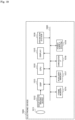
Fig. 19 is a block diagram illustrating a configuration example of an electronic device including the built-in solid-state imaging device to which the present disclosure is applied. - In
Fig. 19 , anelectronic device 1000 includes an imaging system including anoptical system 1011 including a lens group, a solid-state imaging device 1012 having a function corresponding to the solid-state imaging device 10 inFig. 1 , and a Digital Signal Processor (DSP) 1013 that is a camera signal processing unit. In theelectronic device 1000, in addition to the imaging system, a Central Processing Unit (CPU) 1010, aframe memory 1014, adisplay 1015, anoperation system 1016, anauxiliary memory 1017, a communication I/F 1018, and apower supply system 1019 are connected to each another via abus 1020. - The
CPU 1010 controls an operation of each unit of theelectronic device 1000. Theoptical system 1011 captures incident light (image light) from a subject and forms an image on a light detection surface of the solid-state imaging device 1012. The solid-state imaging device 1012 converts the light amount of incident light, with which an image is formed on the light detection surface by theoptical system 1011, into an electrical signal in units of pixels, and outputs the electrical signal as a signal. TheDSP 1013 performs predetermined signal processing on the signal output from the solid-state imaging device 1012. - The
frame memory 1014 temporarily records image data of a still image or a video captured by the imaging system. Thedisplay 1015 is a liquid crystal display or an organic EL display, and displays a still image or a video captured by the imaging system. Theoperation system 1016 issues an operation command for various functions of theelectronic device 1000 in response to a user operation. - The
auxiliary memory 1017 is a storage medium including a semiconductor memory such as a flash memory, and records image data of a still image or a video captured by the imaging system. The communication I/F 1018 has a communication module that supports a predetermined communication method, and transmits image data of a still image or a video captured by the imaging system to other devices via a network. - The
power supply system 1019 appropriately supplies various power supplies functioning as the operating power supply to theCPU 1010, theDSP 1013, theframe memory 1014, thedisplay 1015, theoperation system 1016, theauxiliary memory 1017, and the communication I/F 1018 as supply targets. - Note that the embodiments of the present disclosure are not limited to the above-described embodiments, and various modifications can be made without departing from the essential spirit of the present disclosure. Furthermore, the effects described in this description are merely illustrative and not limiting, and other effects may be obtained.
- The present disclosure can also be configured as follows.
-
- (1) A solid-state imaging device includes:
- a plurality of pixels that each include a photoelectric conversion element and a plurality of wiring capacitive elements; and
- a read-out unit that reads out signals from the plurality of pixels,
- the solid-state imaging device has a structure that a charge having overflown from the photoelectric conversion element is stored in a first wiring capacitive element, and the charge having overflown from the first wiring capacitive element is stored in a second wiring capacitive element, and the read-out unit individually reads out a signal of each of the photoelectric conversion element, the first wiring capacitive element, and the second wiring capacitive element.
- (2) The solid-state imaging device described in above (1), in which the first wiring capacitive element and the second wiring capacitive element are disposed between different wiring layers.
- (3) The solid-state imaging device described in above (1), in which the first wiring capacitive element and the second wiring capacitive element are a first MIM capacitive element and a second MIM capacitive element having different capacitances.
- (4) The solid-state imaging device described in above (3), in which the first MIM capacitive element and the second MIM capacitive element have structures whose at least ones of film types, thicknesses, and areas of dielectrics are different.
- (5) The solid-state imaging device described in above (3) or (4), in which the first MIM capacitive element and the second MIM capacitive element have three-dimensional structures.
- (6) The solid-state imaging device described in any one of (1) to (4), in which the solid-state imaging element has a structure that the charge having overflown from the photoelectric conversion element overflows to the first wiring capacitive element from an overflow path different from a path of a transfer gate that transfers the charge stored in the photoelectric conversion element.
- (7) A solid-state imaging device includes:
- a plurality of pixels that each include a plurality of photoelectric conversion elements and a plurality of wiring capacitive elements; and
- a read-out unit that reads out signals from the plurality of pixels,
- the solid-state imaging device has a structure that a first wiring capacitive element and a second wiring capacitive element are respectively connected to floating diffusions of a first photoelectric conversion element and a second photoelectric conversion element, and a charge having overflown from the first photoelectric conversion element is stored in the first wiring capacitive element, and the charge having overflown from the second photoelectric conversion element is stored in the second wiring capacitive element, and the read-out unit individually reads out a signal of each of the first photoelectric conversion element, the second photoelectric conversion element, the first wiring capacitive element, and the second wiring capacitive element.
- (8) The solid-state imaging device described in above (7), in which the first wiring capacitive element and the second wiring capacitive element are disposed between different wiring layers.
- (9) The solid-state imaging device described in above (7), in which the first wiring capacitive element and the second wiring capacitive element are a first MIM capacitive element and a second MIM capacitive element having different capacitances.
- (10) The solid-state imaging device described in above (9), in which the first MIM capacitive element and the second MIM capacitive element have structures whose at least ones of film types, thicknesses, and areas of dielectrics are different.
- (11) The solid-state imaging device described in above (9) or (10), in which the first MIM capacitive element and the second MIM capacitive element have three-dimensional structures.
- (12) The solid-state imaging device described in any one of (7) to (10), in which the first photoelectric conversion element and the second photoelectric conversion element have different sensitivities.
-
- 10 Solid-state imaging device
- 21 Pixel array unit
- 22 Vertical drive unit
- 23 Column signal processing circuit
- 24 Horizontal drive unit
- 25 Output unit
- 26 Control unit
- 42 Vertical signal line
- 100 Pixel
- 101 Color filter
- 102 On-chip microlens
- 111 Photodiode
- 112, 113 Inter-pixel isolation part
- 121 Inter-wiring layer film
- 122 Wiring
- 131 MIM capacitive element
- 132 MIM capacitive element
- 141 Upper electrode
- 142 Lower electrode
- 143 Dielectric
- 144 Cap film
- 161 Transfer transistor
- 162 FD
- 163 Switch transistor
- 164 Reset transistor
- 165 Amplifier transistor
- 166 Selection transistor
- 167 First storage transistor
- 168 Second storage transistor
- 181 Connection transistor
- 201 Color filter
- 202 On-chip microlens
- 211-1, 211-2 Photodiode
- 212 Inter-pixel isolation part
- 221 Inter-wiring layer film
- 222 Wiring
- 231 MIM capacitive element
- 232 MIM capacitive element
- 261 Transfer transistor
- 262,269 FD
- 263 Switch transistor
- 264 Reset transistor
- 265 Amplifier transistor
- 266 Selection transistor
- 267 Switch transistor
- 268 Storage transistor
- 1000 Electronic device
Claims (12)
- A solid-state imaging device comprising:a plurality of pixels that each include a photoelectric conversion element and a plurality of wiring capacitive elements; anda read-out unit that reads out signals from the plurality of pixels, wherein the solid-state imaging device has a structure that a charge having overflown from the photoelectric conversion element is stored in a first wiring capacitive element, and the charge having overflown from the first wiring capacitive element is stored in a second wiring capacitive element, andthe read-out unit individually reads out a signal of each of the photoelectric conversion element, the first wiring capacitive element, and the second wiring capacitive element.
- The solid-state imaging device according to claim 1, wherein the first wiring capacitive element and the second wiring capacitive element are disposed between different wiring layers.
- The solid-state imaging device according to claim 1, wherein the first wiring capacitive element and the second wiring capacitive element are a first MIM capacitive element and a second MIM capacitive element having different capacitances.
- The solid-state imaging device according to claim 3, wherein the first MIM capacitive element and the second MIM capacitive element have structures whose at least ones of film types, thicknesses, and areas of dielectrics are different.
- The solid-state imaging device according to claim 4, wherein the first MIM capacitive element and the second MIM capacitive element have three-dimensional structures.
- The solid-state imaging device according to claim 5, wherein the solid-state imaging element has a structure that the charge having overflown from the photoelectric conversion element overflows to the first wiring capacitive element from an overflow path different from a path of a transfer gate that transfers the charge stored in the photoelectric conversion element.
- A solid-state imaging device comprising:a plurality of pixels that each include a plurality of photoelectric conversion elements and a plurality of wiring capacitive elements; anda read-out unit that reads out signals from the plurality of pixels, whereinthe solid-state imaging device has a structure that a first wiring capacitive element and a second wiring capacitive element are respectively connected to floating diffusions of a first photoelectric conversion element and a second photoelectric conversion element, and a charge having overflown from the first photoelectric conversion element is stored in the first wiring capacitive element, and the charge having overflown from the second photoelectric conversion element is stored in the second wiring capacitive element, andthe read-out unit individually reads out a signal of each of the first photoelectric conversion element, the second photoelectric conversion element, the first wiring capacitive element, and the second wiring capacitive element.
- The solid-state imaging device according to claim 7, wherein the first wiring capacitive element and the second wiring capacitive element are disposed between different wiring layers.
- The solid-state imaging device according to claim 7, wherein the first wiring capacitive element and the second wiring capacitive element are a first MIM capacitive element and a second MIM capacitive element having different capacitances.
- The solid-state imaging device according to claim 9, wherein the first MIM capacitive element and the second MIM capacitive element have structures whose at least ones of film types, thicknesses, and areas of dielectrics are different.
- The solid-state imaging device according to claim 10, wherein the first MIM capacitive element and the second MIM capacitive element have three-dimensional structures.
- The solid-state imaging device according to claim 7, wherein the first photoelectric conversion element and the second photoelectric conversion element have different sensitivities.
Applications Claiming Priority (2)
| Application Number | Priority Date | Filing Date | Title |
|---|---|---|---|
| JP2022131496 | 2022-08-22 | ||
| PCT/JP2023/028856 WO2024043069A1 (en) | 2022-08-22 | 2023-08-08 | Solid-state imaging device |
Publications (2)
| Publication Number | Publication Date |
|---|---|
| EP4579751A1 true EP4579751A1 (en) | 2025-07-02 |
| EP4579751A4 EP4579751A4 (en) | 2025-12-03 |
Family
ID=90013088
Family Applications (1)
| Application Number | Title | Priority Date | Filing Date |
|---|---|---|---|
| EP23857183.0A Pending EP4579751A4 (en) | 2022-08-22 | 2023-08-08 | Solid-state imaging device |
Country Status (6)
| Country | Link |
|---|---|
| US (1) | US20260032360A1 (en) |
| EP (1) | EP4579751A4 (en) |
| JP (1) | JPWO2024043069A1 (en) |
| CN (1) | CN119563395A (en) |
| TW (1) | TW202425302A (en) |
| WO (1) | WO2024043069A1 (en) |
Families Citing this family (2)
| Publication number | Priority date | Publication date | Assignee | Title |
|---|---|---|---|---|
| TW202549593A (en) * | 2024-03-19 | 2025-12-16 | 日商索尼半導體解決方案公司 | Optical detection elements and electronic devices |
| WO2026018662A1 (en) * | 2024-07-19 | 2026-01-22 | ソニーセミコンダクタソリューションズ株式会社 | Capacitive element and imaging element |
Family Cites Families (15)
| Publication number | Priority date | Publication date | Assignee | Title |
|---|---|---|---|---|
| US6888122B2 (en) * | 2002-08-29 | 2005-05-03 | Micron Technology, Inc. | High dynamic range cascaded integration pixel cell and method of operation |
| JP5066704B2 (en) * | 2005-02-04 | 2012-11-07 | 国立大学法人東北大学 | Solid-state imaging device and method of operating solid-state imaging device |
| US7821560B2 (en) * | 2005-04-07 | 2010-10-26 | Tohoku Universityu | Optical sensor, solid-state imaging device, and operating method of solid-state imaging device |
| JP6719984B2 (en) * | 2016-06-06 | 2020-07-08 | キヤノン株式会社 | Imaging device, imaging system |
| US11050966B2 (en) * | 2017-04-12 | 2021-06-29 | Brillnics Singapore Pte. Ltd. | Solid-state imaging device, method for driving solid-state imaging device, and electronic apparatus |
| US10847316B2 (en) * | 2018-09-20 | 2020-11-24 | Taiwan Semiconductor Manufacturing Co., Ltd. | MIM device with laminated dielectric layers |
| KR102661820B1 (en) * | 2019-02-11 | 2024-05-02 | 삼성전자주식회사 | Image sensor and driving method thereof |
| WO2020241289A1 (en) * | 2019-05-31 | 2020-12-03 | ヌヴォトンテクノロジージャパン株式会社 | Solid-state imaging device and imaging device using same |
| KR102771906B1 (en) * | 2019-11-06 | 2025-02-28 | 삼성전자주식회사 | Memory device, memory system and autonomous driving apparatus |
| CN115066887B (en) * | 2020-02-18 | 2025-10-21 | 新唐科技日本株式会社 | Solid-state imaging device and imaging device using the same |
| US20230307473A1 (en) * | 2020-07-17 | 2023-09-28 | Sony Semiconductor Solutions Corporation | Light receiving element, manufacturing method for same, and electronic device |
| JP7064537B2 (en) * | 2020-07-29 | 2022-05-10 | ソニーセミコンダクタソリューションズ株式会社 | Solid-state image sensor and its control method |
| JP7770323B2 (en) * | 2020-08-19 | 2025-11-14 | ソニーセミコンダクタソリューションズ株式会社 | Solid-state imaging device and electronic device |
| CN116419082A (en) * | 2021-12-31 | 2023-07-11 | 格科微电子(上海)有限公司 | Realization method of high dynamic imaging and its device, image processing system |
| KR20240037026A (en) * | 2022-09-14 | 2024-03-21 | 삼성전자주식회사 | Image sensor |
-
2023
- 2023-07-05 TW TW112125037A patent/TW202425302A/en unknown
- 2023-08-08 US US18/997,324 patent/US20260032360A1/en active Pending
- 2023-08-08 JP JP2024542729A patent/JPWO2024043069A1/ja active Pending
- 2023-08-08 WO PCT/JP2023/028856 patent/WO2024043069A1/en not_active Ceased
- 2023-08-08 EP EP23857183.0A patent/EP4579751A4/en active Pending
- 2023-08-08 CN CN202380052361.8A patent/CN119563395A/en active Pending
Also Published As
| Publication number | Publication date |
|---|---|
| US20260032360A1 (en) | 2026-01-29 |
| EP4579751A4 (en) | 2025-12-03 |
| JPWO2024043069A1 (en) | 2024-02-29 |
| WO2024043069A1 (en) | 2024-02-29 |
| CN119563395A (en) | 2025-03-04 |
| TW202425302A (en) | 2024-06-16 |
Similar Documents
| Publication | Publication Date | Title |
|---|---|---|
| US11665452B2 (en) | Image sensor | |
| EP2758937B1 (en) | Stacked-chip imaging systems | |
| CN209845132U (en) | Pixel circuit of solid-state high dynamic range image sensor and said image sensor | |
| EP2230690B1 (en) | Solid-state imaging device, method of manufacturing the same, method of driving the same, and electronic apparatus | |
| US7008816B2 (en) | Imager photo diode capacitor structure with reduced process variation sensitivity | |
| US10777601B1 (en) | CMOS image sensor with compact pixel layout | |
| CN108200367A (en) | Pixel unit and the formation method of pixel unit and digital camera imaging system components | |
| US7847847B2 (en) | Structure for CMOS image sensor with a plurality of capacitors | |
| CN108282625A (en) | Pixel unit and the method and digital camera imaging system components for forming pixel unit | |
| US12610646B2 (en) | Image sensor | |
| CN108305884A (en) | Pixel unit and the method and digital camera imaging system components for forming pixel unit | |
| US20260032360A1 (en) | Solid-state imaging device | |
| US20150123173A1 (en) | 3d stacked image sensor with pmos components | |
| KR20220152457A (en) | Image sensor and operating method thereof | |
| CN116525635A (en) | CMOS image sensor, forming method thereof and vehicle-mounted camera | |
| US12356741B2 (en) | Split floating diffusion pixel layout design | |
| TWI925056B (en) | Pixel array and imaging system of split floating diffusion pixel layout design | |
| US20250212546A1 (en) | Image sensor including stacked capacitors | |
| US12047694B2 (en) | Split floating diffusion pixel layout design | |
| US20250160030A1 (en) | Image sensor | |
| WO2025004565A1 (en) | Optical detection device and electronic apparatus | |
| KR20070050593A (en) | Image sensor and its manufacturing method |
Legal Events
| Date | Code | Title | Description |
|---|---|---|---|
| STAA | Information on the status of an ep patent application or granted ep patent |
Free format text: STATUS: THE INTERNATIONAL PUBLICATION HAS BEEN MADE |
|
| PUAI | Public reference made under article 153(3) epc to a published international application that has entered the european phase |
Free format text: ORIGINAL CODE: 0009012 |
|
| STAA | Information on the status of an ep patent application or granted ep patent |
Free format text: STATUS: REQUEST FOR EXAMINATION WAS MADE |
|
| 17P | Request for examination filed |
Effective date: 20250109 |
|
| AK | Designated contracting states |
Kind code of ref document: A1 Designated state(s): AL AT BE BG CH CY CZ DE DK EE ES FI FR GB GR HR HU IE IS IT LI LT LU LV MC ME MK MT NL NO PL PT RO RS SE SI SK SM TR |
|
| REG | Reference to a national code |
Ref country code: DE Ref legal event code: R079 Free format text: PREVIOUS MAIN CLASS: H01L0027146000 Ipc: H10F0039000000 |
|
| DAV | Request for validation of the european patent (deleted) | ||
| DAX | Request for extension of the european patent (deleted) | ||
| A4 | Supplementary search report drawn up and despatched |
Effective date: 20251103 |
|
| RIC1 | Information provided on ipc code assigned before grant |
Ipc: H10F 39/00 20250101AFI20251028BHEP Ipc: H04N 25/59 20230101ALI20251028BHEP Ipc: H04N 25/771 20230101ALI20251028BHEP Ipc: H10F 39/12 20250101ALI20251028BHEP Ipc: H10F 39/18 20250101ALI20251028BHEP |