CN116419082A - Method and device for realizing high dynamic imaging and image processing system - Google Patents
Method and device for realizing high dynamic imaging and image processing system Download PDFInfo
- Publication number
- CN116419082A CN116419082A CN202111657558.3A CN202111657558A CN116419082A CN 116419082 A CN116419082 A CN 116419082A CN 202111657558 A CN202111657558 A CN 202111657558A CN 116419082 A CN116419082 A CN 116419082A
- Authority
- CN
- China
- Prior art keywords
- voltage
- unit
- signal
- column
- gain
- Prior art date
- Legal status (The legal status is an assumption and is not a legal conclusion. Google has not performed a legal analysis and makes no representation as to the accuracy of the status listed.)
- Pending
Links
- 238000012545 processing Methods 0.000 title claims abstract description 92
- 238000000034 method Methods 0.000 title claims abstract description 39
- 238000003384 imaging method Methods 0.000 title claims abstract description 28
- 238000006243 chemical reaction Methods 0.000 claims abstract description 201
- 206010034972 Photosensitivity reaction Diseases 0.000 claims abstract description 29
- 230000036211 photosensitivity Effects 0.000 claims abstract description 29
- 238000007667 floating Methods 0.000 claims description 80
- 238000009792 diffusion process Methods 0.000 claims description 63
- 238000012546 transfer Methods 0.000 claims description 20
- 239000000969 carrier Substances 0.000 claims description 7
- 230000035945 sensitivity Effects 0.000 claims description 4
- 238000013139 quantization Methods 0.000 claims description 3
- 230000007704 transition Effects 0.000 claims description 3
- 206010034960 Photophobia Diseases 0.000 claims 1
- 208000013469 light sensitivity Diseases 0.000 claims 1
- 230000000875 corresponding effect Effects 0.000 description 42
- 238000010586 diagram Methods 0.000 description 16
- 102100040678 Programmed cell death protein 1 Human genes 0.000 description 10
- 230000009977 dual effect Effects 0.000 description 9
- 239000003990 capacitor Substances 0.000 description 4
- 230000001276 controlling effect Effects 0.000 description 4
- 101710089372 Programmed cell death protein 1 Proteins 0.000 description 3
- 238000012986 modification Methods 0.000 description 3
- 230000004048 modification Effects 0.000 description 3
- 238000009825 accumulation Methods 0.000 description 2
- 230000005540 biological transmission Effects 0.000 description 2
- 238000005516 engineering process Methods 0.000 description 2
- 238000012544 monitoring process Methods 0.000 description 2
- 101100046653 Arabidopsis thaliana TOR1L1 gene Proteins 0.000 description 1
- 230000009286 beneficial effect Effects 0.000 description 1
- 238000004891 communication Methods 0.000 description 1
- 230000002596 correlated effect Effects 0.000 description 1
- 238000013461 design Methods 0.000 description 1
- 238000005070 sampling Methods 0.000 description 1
- 230000000007 visual effect Effects 0.000 description 1
Images


Classifications
-
- H—ELECTRICITY
- H04—ELECTRIC COMMUNICATION TECHNIQUE
- H04N—PICTORIAL COMMUNICATION, e.g. TELEVISION
- H04N9/00—Details of colour television systems
- H04N9/77—Circuits for processing the brightness signal and the chrominance signal relative to each other, e.g. adjusting the phase of the brightness signal relative to the colour signal, correcting differential gain or differential phase
-
- H—ELECTRICITY
- H04—ELECTRIC COMMUNICATION TECHNIQUE
- H04N—PICTORIAL COMMUNICATION, e.g. TELEVISION
- H04N23/00—Cameras or camera modules comprising electronic image sensors; Control thereof
- H04N23/70—Circuitry for compensating brightness variation in the scene
- H04N23/741—Circuitry for compensating brightness variation in the scene by increasing the dynamic range of the image compared to the dynamic range of the electronic image sensors
-
- H—ELECTRICITY
- H04—ELECTRIC COMMUNICATION TECHNIQUE
- H04N—PICTORIAL COMMUNICATION, e.g. TELEVISION
- H04N25/00—Circuitry of solid-state image sensors [SSIS]; Control thereof
- H04N25/50—Control of the SSIS exposure
- H04N25/57—Control of the dynamic range
-
- H—ELECTRICITY
- H04—ELECTRIC COMMUNICATION TECHNIQUE
- H04N—PICTORIAL COMMUNICATION, e.g. TELEVISION
- H04N25/00—Circuitry of solid-state image sensors [SSIS]; Control thereof
- H04N25/70—SSIS architectures; Circuits associated therewith
- H04N25/76—Addressed sensors, e.g. MOS or CMOS sensors
Abstract
The invention provides a method for realizing high dynamic imaging, a device and an image processing system thereof, wherein the high dynamic imaging device comprises an image sensor, and a pixel array in the image sensor comprises a plurality of pixel units; the column processing unit comprises a gain control unit and an analog-to-digital conversion unit; the pixel unit comprises two photoelectric conversion units with different photosensitivity; the gain control unit is used for judging the brightness range of the image according to the signal voltage output by the pixel unit, and selecting a photoelectric conversion unit for signal conversion in the pixel unit, a charge-voltage conversion gain of the pixel unit and a voltage gain of the column processing unit according to the brightness range. The method and the device for realizing the high dynamic imaging can read out the primary signal voltage by image processing, shorten the line reading time and further improve the frame rate.
Description
Technical Field
The present invention relates to the field of image sensors, and in particular, to a method and apparatus for implementing high dynamic imaging, and an image processing system.
Background
Compared with a common image, the High-Dynamic Range image (HDR) can provide more Dynamic Range and image details, and a final HDR image is synthesized by utilizing the LDR image with the optimal details corresponding to each exposure time according to the LDR (Low-Dynamic Range) images with different exposure times, so that the visual effect in a real environment can be better reflected.
CMOS image sensors (CMOS image sensor, CIS) are widely used in various fields such as mobile phones, monitoring security, machine vision, consumer electronics, and the like, and expansion of application fields puts forward higher requirements on performance indexes of CIS. Dynamic range (dynamic range) is one of important indexes of CIS, and is particularly critical in complex application scenes such as security monitoring and automatic driving.
The high dynamic range image sensor HDRCIS has various implementation methods, for example, a final image with a high dynamic range can be obtained by fusing a plurality of images with different exposure times, and the final image can also be obtained by including two photodiodes with different photosensitivity in one pixel, and a technology of applying the pixel structure is called a dual conversion gain (dual conversion gain, DCG) pixel structure or a split diode (split photodiode pixel, SPP) pixel structure.
In recent years, dual photodiode has gained some attention and application in HDR CIS design, and derives the dcg+dual photodiode (dual photodiode) structure, but the whole readout period is longer and the speed is slower.
For example, there is a three capture High Dynamic Range (HDR) CMOS image sensor in the prior art that combines split diode pixel technology with Dual Conversion Gain (DCG) readout to achieve HDR and eliminate LED flicker (LEDflickermitigation, LFM). The specific pixel circuit diagram and the readout timing diagram are shown in fig. 1 and fig. 2, respectively.
The pixel includes: a photodiode LPD with a larger photosensitivity, a photodiode SPD with a smaller photosensitivity, a transfer gate TXL of LPD, a transfer gate TXS of SPD, a floating diffusion DFD, a reset transistor RST, a pixel source follower transistor SF and a select transistor RS.
Wherein the floating diffusion node FD (flating diffusion) of the photodiode LPD and photodiode SPD are separated by a DFD transistor into FD1 and FD2. The low conversion gain is obtained by increasing the gate equivalent capacitance C of the pixel source follower transistor SF by using the floating diffusion gate DFD between FD1 and FD2. The high conversion gain CG is obtained by switching off the DFD. The charge of the photodiode LPD with greater photosensitivity can be sensed in both the low conversion gain mode LCG and the high conversion gain mode HCG, while the photodiode SPD with lesser photosensitivity can only be read out in the LCG mode.
Thus the sensor can acquire three sensing values, namely: the photo diode LPD with greater photosensitivity is exposed to HCG acquired under high conversion gain, the photo diode LPD with greater photosensitivity is exposed to LCG acquired under low conversion gain, and the photo diode (SPD) with lesser photosensitivity is exposed to SPD acquired under low conversion gain, respectively.
The three sensing values of HCG, LCG and SPD are read out using a digital correlated double sampling circuit and then digitally combined to form a linear output pixel value.
The pixel structure and operation timing of another high dynamic range image sensor of the prior art are shown in fig. 3 and 4. In which fig. 3 shows a simplified schematic diagram of a pixel of a high dynamic range image sensor. The pixel employs a large photodiode SP1, a small photodiode SP2, a floating capacitor FC within the pixel, and seven transistors. The sensitivity of SP2 is less than that of SP 1. The seven transistors are: transfer gate TGL of SP1, transfer gate TGS of SP2, floating diffusion gate FDG, floating capacitance gate FCG, reset transistor RST, select transistor SEL, source follower amplifier AMP. The FDG and FCG separate the floating diffusion node FD (flatingdiffusion) into FD1, FD2, and FD3, and serve as switches connecting FD1, FD2, and FD 3. The two electrodes of FC are connected to FD3 and a counter electrode whose power supply voltage VDD is FC VDD, respectively.
The simplified timing diagram is shown in fig. 4. The charge accumulated in SP1 is converted into two modes, i.e., a high conversion gain mode (SP 1H) and a low conversion gain mode (SP 1L) by the FDG switch. The charge accumulated in SP2 is read out as SP2H. The charge accumulates and is combined with SP2 and read out as SP2L. Thus, four signals can be read out by one exposure. The signal with the highest signal-to-noise ratio is selected for each pixel and then an image is synthesized.
As can be seen from the above two prior arts, the first prior art HDR is realized by stitching a high dynamic range image with a plurality of sets of readout data, and in this structure, at least 3 sets of signals (signals) and reset (reset) are required for realizing the HDR, for a total of 6 data.
Whereas the second prior art described above requires reading out 4 sets of signals (signals) and reset (reset), for a total of 8 data.
As is clear from this, in the related art, the amount of data to be read in order to realize an image with a high dynamic range is large, and the read period is long.
Disclosure of Invention
The invention aims to provide a novel implementation method of a high dynamic range (high dynamic range, HDR) image sensor, which shortens a reading period and realizes a CMOS image sensor with high dynamic range.
In order to solve the technical problems, the present invention provides a method for implementing high dynamic imaging, which is implemented based on an image sensor, wherein a pixel unit of the image sensor has a plurality of charge-voltage conversion gain steps, a column signal processing unit of the image sensor has a plurality of voltage gain steps, and the pixel unit comprises two photoelectric conversion units with different photosensitivity;
the implementation method comprises the following steps:
clearing the photoelectric conversion units of the pixel units in the current row;
integrating the photogenerated carriers on each photoelectric conversion unit in the current row;
resetting the floating diffusion area of each pixel unit in the current row;
setting the charge-voltage conversion gain gear of each pixel unit of the current row;
setting a voltage gain gear of a column signal processing unit of the image sensor;
converting and storing a conversion reference value of the reference voltage after the floating diffusion area is reset in a specific gear setting state or a plurality of conversion reference values of a plurality of gear setting states;
controlling a transfer transistor of each pixel unit in the current row to transfer all or part of photogenerated carriers of each pixel unit from the photoelectric conversion unit with higher photosensitivity to a corresponding floating diffusion region;
each column of signal processing units detects the signal voltage of the floating diffusion region of the pixel unit corresponding to the column, and correspondingly selects the photoelectric conversion unit for signal conversion in the pixel unit corresponding to the column;
each column of signal processing units detects the signal voltage of the floating diffusion region of the pixel unit corresponding to the column, and correspondingly sets the charge-voltage conversion gain gear of the pixel unit corresponding to the column;
each column of signal processing units detects the signal voltage of the floating diffusion region of the pixel unit corresponding to the column, and correspondingly sets the voltage gain gear of the column of signal processing units;
each column of signal processing units simultaneously converts the signal voltage of the floating diffusion region of the corresponding pixel unit to obtain a conversion signal value of the current row;
and processing the conversion signal value and one or more conversion reference values to obtain the image signal value of each pixel unit of the current row in the corresponding gear.
Preferably, the brightness range of the image is judged according to the signal voltage output by the pixel unit.
Preferably, the photoelectric conversion unit that performs signal conversion in the pixel unit, the charge-voltage conversion gain of the pixel unit, and the voltage gain of the column processing unit are adjusted according to the luminance range.
Preferably, the different column signal processing units of the current row have different voltage gain steps.
Preferably, the gain shift voltage is provided to be compared with the output signal voltage of the pixel unit one or more times so as to judge the brightness range of the current image.
Preferably, control signals for selecting a photoelectric conversion unit in the pixel unit, converting a gain setting, and setting a voltage gain of the column processing unit are generated according to a luminance range in which the image is located.
Preferably, different pixel cells of the current row have different charge-to-voltage conversion gain steps.
Preferably, the different pixel units of the current row select photoelectric conversion units with different photosensitivity for signal conversion.
Preferably, the step of detecting the signal voltage of the floating diffusion region of the pixel unit corresponding to the column by each column signal processing unit, selecting the photoelectric conversion unit for signal conversion in the pixel unit corresponding to the column accordingly, setting the charge-voltage conversion gain shift of the pixel unit, and setting the voltage gain shift of the signal processing unit of the column includes:
setting a plurality of gear combinations according to the sensitivity of the photoelectric conversion unit, the voltage gain gear and the charge-voltage conversion gain gear, wherein each gear combination corresponds to a different voltage interval;
and judging a voltage interval in which the detected signal voltage of the floating diffusion area is located, further determining the gear combination corresponding to the voltage interval, simultaneously selecting a photoelectric conversion unit for signal conversion, and setting the voltage gain gear and the charge-voltage conversion gain gear.
Preferably, the detecting, by each column of signal processing units, the signal voltage of the floating diffusion region of the pixel unit corresponding to the column, selecting, accordingly, the photoelectric conversion unit for performing signal conversion in the pixel unit corresponding to the column, setting the charge-voltage conversion gain gear of the pixel unit, and setting the voltage gain gear of the signal processing unit of the column includes:
determining a signal processing unit voltage gain gear corresponding to the signal voltage according to the detected signal voltage of the floating diffusion region and a preset first voltage interval;
determining a charge-voltage conversion gain gear of a pixel unit corresponding to the signal voltage according to the detected signal voltage of the floating diffusion region and a preset second voltage interval;
and determining a photoelectric conversion unit for performing signal conversion in the pixel unit corresponding to the signal voltage according to the detected signal voltage of the floating diffusion region and a preset third voltage interval.
Preferably, the image signal is divided into a plurality of sub-segments according to the voltage gain shift and the charge-voltage conversion gain shift, and each of the signal processing units performs signal quantization according to the selected corresponding sub-segment while outputting the image signal.
Preferably, the image signals in each sub-segment are processed according to a preset mode, so that the image curves fitted by the image signals in each sub-segment can be sequentially connected end to end and output.
Preferably, the image signal output corresponding to the start portion and the end portion of each of the sub-segment sections is linearly changed, and the image signal output corresponding to the remaining portion is non-linearly changed.
Preferably, for a plurality of sub-segments of the image signal, a start portion of each sub-segment has the same gain as an end portion of a preceding sub-segment, such that the image curve smoothly transitions between adjacent sub-segments.
The technical scheme of the invention also provides a high dynamic imaging device, which comprises an image sensor and further comprises:
a pixel array in the image sensor, including a plurality of pixel units;
the column processing unit comprises a gain control unit and an analog-to-digital conversion unit;
the pixel unit comprises two photoelectric conversion units with different photosensitivity;
the gain control unit is used for judging the brightness range of the image according to the signal voltage output by the pixel unit, and selecting a photoelectric conversion unit for signal conversion in the pixel unit, a charge-voltage conversion gain of the pixel unit and a voltage gain of the column processing unit according to the brightness range.
Preferably, the gain control unit includes:
the gain gear voltage providing unit is suitable for providing one or more times of comparison between the gain gear voltage and the output signal voltage of the pixel unit so as to judge the brightness range of the current image;
and the gain control signal generating unit is used for generating control signals for selecting, converting gain setting and voltage gain setting of the column processing unit of the photoelectric conversion unit in the pixel unit according to the brightness range of the current image.
Preferably, the pixel unit further includes a floating diffusion region, the photoelectric conversion units respectively include a photoelectric conversion portion and a transfer gate adapted to transfer charges in the photoelectric conversion portion to the floating diffusion region.
Preferably, the photoelectric conversion units are a first photoelectric conversion unit and a second photoelectric conversion unit, respectively; a first switch unit is arranged between the first photoelectric conversion unit and the second photoelectric conversion unit, and the first switch unit is suitable for switching different photoelectric conversion units to be communicated with the column processing unit.
Preferably, the first photoelectric conversion unit has a higher photosensitivity than the second photoelectric conversion unit.
The technical scheme of the invention also provides an image processing system, which comprises:
the high dynamic imaging device as described above;
a row driving unit;
the pixel units in the same row are connected to the same row control line, and the row driving unit drives and controls the pixel units through the row control line;
the same column of pixel units is connected to the same column signal line, and output signals of the pixel units are output to a column processing unit through the column signal line;
the same column of pixel units is connected to the same column control line, and the column processing unit drives and controls the pixel units through the column control line.
Preferably, the display device further comprises a column storage unit, and the column processing unit stores the modulus result of the output signal of the pixel unit in the column storage unit.
Compared with the prior art, the method and the device for realizing the high dynamic imaging and the image processing system have the following beneficial effects:
before analog-to-digital conversion is carried out on the signal voltage read out by the pixel, pre-judging is carried out for one time, the brightness range where the pixel output voltage range is judged is located, and the conversion gain of the pixel is adaptively adjusted, so that the signal voltage can be read out for one time, the line reading time is shortened, and the frame rate is further improved.
Furthermore, in the technical scheme provided by the invention, under the dual photodiode structure, the signal paths of the two photoelectric conversion units can be respectively subjected to self-adaptive conversion gain control, and only two signal voltages are read out, so that the pixel signal readout control of a four-gear brightness interval can be realized.
Furthermore, in the technical scheme provided by the invention, the floating charge conduction transistor and the floating charge storage capacitor which are introduced in the floating diffusion region of the second photoelectric conversion unit with lower photosensitivity can realize accumulation of overflowing charges in the exposure process of the floating diffusion region of the second photoelectric conversion unit with lower photosensitivity under extremely high brightness, so that the dynamic range of imaging is further improved.
Furthermore, the technical scheme provided by the invention avoids the condition that four signal voltages need to be read out for realizing the pixel signal reading of the four-gear brightness interval based on the dual photo diode structure in the prior art, reduces the requirements on data processing and storage, and saves chip resources and power consumption.
Drawings
FIG. 1 is a circuit diagram of a pixel structure of a high dynamic range CMOS image sensor according to the prior art;
FIG. 2 is a readout timing diagram of a pixel structure of the high dynamic range CMOS image sensor shown in FIG. 1;
FIG. 3 is a circuit diagram of a pixel structure of another high dynamic range image sensor according to the prior art;
FIG. 4 is a readout timing diagram of a pixel structure of the high dynamic range image sensor shown in FIG. 3;
FIG. 5 is a flowchart of a method for implementing a high-dynamic image sensor according to an embodiment of the present invention;
FIG. 6 is a block diagram of a high dynamic imaging device according to an embodiment of the present invention;
fig. 7 is a circuit diagram of a pixel structure in a high-dynamic image sensor in one embodiment;
FIG. 8 is a schematic diagram of a readout timing of the pixel structure shown in FIG. 7;
fig. 9 is a circuit diagram of a pixel structure in a high-dynamic image sensor in another embodiment;
FIG. 10 is a schematic diagram of an image processing system according to an embodiment of the present invention;
fig. 11 is an image processing system according to another embodiment of the present invention.
Detailed Description
The technical scheme provided by the invention aims at providing a novel implementation method of the CIS with high dynamic range on the basis of combining a method for adaptively controlling DCG and a dual photodiode structure.
In the following description, numerous specific details are set forth in order to provide a thorough understanding of the present invention. The present invention may be embodied in many other forms than those herein described, and those skilled in the art will readily appreciate that the present invention may be similarly embodied without departing from the spirit or essential characteristics thereof, and therefore the present invention is not limited to the specific embodiments disclosed below.
Next, the present invention will be described in detail with reference to the drawings, which are only examples for convenience of illustration, and should not be construed as limiting the scope of the invention.
In order to make the above objects, features and advantages of the present invention more comprehensible, a method for implementing the present invention with high dynamic imaging will be described in detail with reference to the accompanying drawings.
Fig. 5 is a flowchart of a method for implementing a high-dynamic image sensor according to an embodiment of the present invention. Specifically, the pixel unit of the image sensor provided by the embodiment of the invention has a plurality of charge-voltage conversion gain steps, the column signal processing unit of the image sensor has a plurality of voltage gain steps, and the pixel unit comprises two photoelectric conversion units with different photosensitivity;
the implementation method comprises the following steps:
step S101 is performed: clearing the photoelectric conversion units of the pixel units in the current row;
step S102 is performed: integrating the photogenerated carriers on each photoelectric conversion unit in the current row;
step S103 is performed: resetting the floating diffusion area of each pixel unit in the current row;
step S104 is performed: setting the charge-voltage conversion gain gear of each pixel unit of the current row;
step S105 is performed: setting a voltage gain gear of a column signal processing unit of the image sensor;
step S106 is executed: converting and storing a conversion reference value of the reference voltage after the floating diffusion area is reset in a specific gear setting state or a plurality of conversion reference values of a plurality of gear setting states;
step S107 is performed: controlling a transfer transistor of each pixel unit in the current row to transfer all or part of photogenerated carriers of each pixel unit from the photoelectric conversion unit with higher photosensitivity to a corresponding floating diffusion region;
step S108 is performed: each column of signal processing units detects the signal voltage of the floating diffusion region of the pixel unit corresponding to the column, and correspondingly selects the photoelectric conversion unit for signal conversion in the pixel unit corresponding to the column;
step S109 is performed: each column of signal processing units detects the signal voltage of the floating diffusion region of the pixel unit corresponding to the column, and correspondingly sets the charge-voltage conversion gain gear of the pixel unit corresponding to the column;
step S110 is performed: each column of signal processing units detects the signal voltage of the floating diffusion region of the pixel unit corresponding to the column, and correspondingly sets the voltage gain gear of the column of signal processing units;
step S111 is performed: each column of signal processing units simultaneously converts the signal voltage of the floating diffusion region of the corresponding pixel unit to obtain a conversion signal value of the current row;
further, in the step, the signal processing units in different columns of the current row may have different voltage gain steps, the pixel units in different columns of the current row may have different charge-voltage conversion gain steps, and the pixel units in different columns of the current row may select photoelectric conversion units with different photosensitivity to perform signal conversion;
step S112 is performed: and processing the conversion signal value and the one or more conversion reference values to obtain the image signal value of each pixel unit of the current row in the corresponding gear.
Preferably, the step of detecting the signal voltage of the floating diffusion region of the pixel unit corresponding to the column by each column signal processing unit, selecting the photoelectric conversion unit for signal conversion in the pixel unit corresponding to the column accordingly, setting the charge-voltage conversion gain shift of the pixel unit, and setting the voltage gain shift of the signal processing unit of the column includes:
setting a plurality of gear combinations according to the sensitivity of the photoelectric conversion unit, the voltage gain gear and the charge-voltage conversion gain gear, wherein each gear combination corresponds to a different voltage interval;
and judging a voltage interval in which the detected signal voltage of the floating diffusion area is located, further determining the gear combination corresponding to the voltage interval, simultaneously selecting a photoelectric conversion unit for signal conversion, and setting the voltage gain gear and the charge-voltage conversion gain gear.
Preferably, the detecting, by each column of signal processing units, the signal voltage of the floating diffusion region of the pixel unit corresponding to the column, selecting, accordingly, the photoelectric conversion unit for performing signal conversion in the pixel unit corresponding to the column, setting the charge-voltage conversion gain gear of the pixel unit, and setting the voltage gain gear of the signal processing unit of the column includes:
determining a signal processing unit voltage gain gear corresponding to the signal voltage according to the detected signal voltage of the floating diffusion region and a preset first voltage interval;
determining a charge-voltage conversion gain gear of a pixel unit corresponding to the signal voltage according to the detected signal voltage of the floating diffusion region and a preset second voltage interval;
and determining a photoelectric conversion unit for performing signal conversion in the pixel unit corresponding to the signal voltage according to the detected signal voltage of the floating diffusion region and a preset third voltage interval.
Preferably, the image signal is divided into a plurality of sub-segments according to the voltage gain shift and the charge-voltage conversion gain shift, and each of the signal processing units performs signal quantization according to the selected corresponding sub-segment while outputting the image signal.
Preferably, the image signals in each sub-segment are processed according to a preset mode, so that the image curves fitted by the image signals in each sub-segment can be sequentially connected end to end and output.
Preferably, the image signal output corresponding to the start portion and the end portion of each of the sub-segment sections is linearly changed, and the image signal output corresponding to the remaining portion is non-linearly changed.
Preferably, for a plurality of sub-segments of the image signal, a start portion of each sub-segment has the same gain as an end portion of a preceding sub-segment, such that the image curve smoothly transitions between adjacent sub-segments.
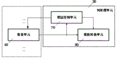
Referring to fig. 6, the technical scheme of the present invention further provides a high dynamic imaging device, where the high dynamic imaging device includes an image sensor, and specifically further includes:
a pixel array in the image sensor, comprising a plurality of pixel units 40;
a column processing unit including a gain control unit 70 and an analog-to-digital conversion unit 80;
the pixel unit 40 includes two photoelectric conversion units having different photosensitivity;
the gain control unit 70 is configured to determine a brightness range in which an image is located according to a signal voltage output by the pixel unit 40, and adjust a photoelectric conversion unit that performs signal conversion in the pixel unit, a charge-voltage conversion gain of the pixel unit, and a voltage gain of the column processing unit according to the brightness range.
Specifically, the gain control unit 70 includes:
the gain gear voltage providing unit is suitable for providing one or more times of comparison between the gain gear voltage and the output signal voltage of the pixel unit so as to judge the brightness range of the current image;
and the gain control signal generating unit is used for generating control signals for selecting, converting gain setting and voltage gain setting of the column processing unit of the photoelectric conversion unit in the pixel unit according to the brightness range of the image.
Referring to fig. 7, 8 and 9 in combination with fig. 6, fig. 7 is a circuit diagram of a pixel structure in a high-dynamic image sensor according to one embodiment, fig. 8 is a readout timing diagram of the pixel structure shown in fig. 7, and fig. 9 is a circuit diagram of a pixel structure in a high-dynamic image sensor according to another embodiment.
In the pixel structure shown in fig. 7 or 9, two photoelectric conversion units having different photosensitivity are included, the photoelectric conversion units respectively including a first photoelectric conversion unit PD1 and a second photoelectric conversion unit PD2. In the present embodiment, the photosensitivity of the first photoelectric conversion unit PD1 is higher than the photosensitivity of the second photoelectric conversion unit PD2.
In this embodiment, the photoelectric conversion unit includes a photoelectric conversion portion and a transfer gate, respectively, the pixel unit further includes a floating diffusion FD, and the transfer gate is adapted to transfer charges in the photoelectric conversion portion to the floating diffusion FD. In this embodiment, the transmission gate is a transmission transistor TXL and TXS.
In this embodiment, a first switching unit DCG is disposed between the first photoelectric conversion unit and the second photoelectric conversion unit, and the first switching unit DCG is adapted to switch different communication column processing units of the photoelectric conversion units.
The photoelectric conversion unit and the floating diffusion FD are arranged between a first reference voltage Vref1 and a second reference voltage Vref2, a first reference voltage gating transistor is arranged between the floating diffusion FD and the first reference voltage Vref1, and a reset transistor RST is arranged between the floating diffusion FD and the second reference voltage Vref 2.
The first photoelectric conversion unit PD1 is connected to a gate of a first reference voltage gating transistor, a source drain of the first reference voltage gating transistor is connected to the first reference voltage Vref1 and the column gating transistor SEL, respectively, and a gate of the SEL column gating transistor is connected to a column gating signal.
One end of the second photoelectric conversion unit PD2 facing the floating diffusion FD is provided with a floating charge storage area CF, one end of the floating charge storage area CF, which is far from the second photoelectric conversion unit PD2, is connected to a power supply voltage VSSC, and the floating charge storage area CF is adapted to store electrons overflowed from the second photoelectric conversion unit PD2 during exposure and provide different conversion gains when being accessed. In this embodiment, the floating charge storage region CF is a capacitor.
The supply voltage VSSC may be a high level, a low level, or a varying waveform voltage according to the capacitance structure of the floating charge storage region CF.
A floating charge pass transistor TGC is further provided between the second photoelectric conversion units in the floating charge storage region, and is adapted to pass the floating charge storage region CF when necessary.
In this embodiment, the floating charge turn-on transistor TGC and the floating charge storage area (capacitor) CF introduced in the floating diffusion region FD of the second photoelectric conversion unit PD2 with lower photosensitivity can realize accumulation of overflowing charges in the exposure process of the PD2 under extremely high brightness, thereby further improving the dynamic range.
As shown with reference to fig. 7, a second switching transistor TGS is provided between the floating charge storage region (CF) and the floating diffusion region.
Referring to fig. 9, a fourth switching unit RGC connected in parallel with the floating charge turn-on transistor TGC is further disposed between the second photoelectric conversion units in the floating charge storage region to control access of exposure time to the floating charge storage region. A fifth switching unit TGX is further disposed between the first switching unit DCG and the second photoelectric conversion unit.
In this embodiment, the first photoelectric conversion unit includes a first transfer gate TX1 and a first photoelectric conversion unit PD1.
The second photoelectric conversion unit includes a second transfer gate TX2 and a second photoelectric conversion unit PD2.
In the above embodiment, one reference voltage is provided in each of the two pre-judgments, and the DCG and TGC switches are determined according to the judging result, so that the readout processes of the two PDs are independent, and two signal voltage readouts are required.
Referring to fig. 11, the readout timing thereof. Before the process of the readout timing shown in fig. 11, further includes:
clearing the photoelectric conversion units PD1 and PD2 of each pixel unit in the current row;
integrating photo-generated carriers on each of the photoelectric conversion units PD1 and PD2 in the current row;
resetting the floating diffusion FD of each of the pixel units 40 of the current row;
setting the charge-voltage conversion gain gear of each pixel unit of the current row;
setting a voltage gain gear of a column signal processing unit of the image sensor;
specifically, the detailed procedure of the readout timing shown in fig. 11 is as follows:
1) Setting a DCG signal to be high, starting a DCG tube, and reading out FD node Reference voltage R1L (Reference/PD 1/Low CG);
2) The DCG signal is low, the DCG tube is turned off, and the Reference voltage R1H (Reference/PD 1/High CG) of the FD node is read out
Converting and saving a conversion reference value reference voltage R1L and a reference voltage R1H of the floating diffusion region in a specific gear setting state through the stages 1) and 2);
3) Turning on a transfer transistor TX1 of each pixel unit in the current row, and transferring electrons accumulated in PD1 to FD in the exposure process;
each column signal processing unit detects the signal voltage FD node voltage of the floating diffusion region of the pixel unit corresponding to the column, performs a first pre-judgment section, and correspondingly sets the charge-voltage conversion gain gear of the pixel unit corresponding to the column, specifically:
if PXD < Vref1, judging that the current brightness is higher, making dcg=1, otherwise, judging that the current brightness is lower, making dcg=0;
4) And according to the judging result of the stage 3), each column of signal processing units simultaneously converts the signal voltage of the floating diffusion region of the corresponding pixel unit to obtain the conversion signal value of the current row. Specifically, the DCG tube is controlled to be turned on or off, TX1 is turned on once again, and then the Signal voltage S1 (Signal/PD 1) of the FD node is read out;
5) Keeping the DCG tube and the TGS tube open, briefly starting the RST tube, reading out the Reference voltage R2H (Reference/PD 2/High CG) TX2 tube of the FD node to open, transferring electrons accumulated in PD2 to FD in the exposure process, reading out the voltage of the FD node, performing a second pre-judgment section, if PXD < Vref2, the Reference voltage is in extremely bright brightness, enabling TGC=1, otherwise enabling TGC=0;
6) According to the judging result of the stage 6), controlling the TGC tube to be turned on or turned off, enabling the TX2 to be turned on once again, and then reading out the Signal voltage S2 (Signal/PD 2) of the FD node;
7) The TGC tube is kept on, the RST tube is turned on briefly, and the Reference voltage R2L (Reference/PD 2/Low CG) of the FD node is read out;
description: vref1 and Vref2 may be the same or different.
Fig. 10 shows an image processing system according to an embodiment of the present invention. Comprising the following steps:
the high dynamic imaging device 50 as described above;
a row driving unit 30;
the pixel units 40 of the same row are connected to the same row control line LL, and the row driving unit 30 drives and controls the pixel units through the row control line LL;
the same column pixel units are connected to the same column signal line CL via which output signals of the pixel units are output to the column processing unit 20.
The same column of pixel cells is connected to the same column control line CC through which the column processing unit drives and controls the pixel cells.
Further, referring to fig. 11, the image processing system according to another embodiment of the present invention further includes a column storage unit 10, and the column processing unit 20 stores the modulus result of the output signal to the pixel unit in the column storage unit 10.
In the image processing system provided by the technical scheme of the invention, after the column processing unit detects the image brightness interval, the gain control unit can switch the conversion gain of the pixel unit on the basis of adjusting the analog gain of the output signal of the pixel unit, especially for a pixel structure with a plurality of photodiodes, the switching can be self-adaptively performed on the selection of the photodiodes, the frequency and time for reading data are reduced, the requirements for data processing and storage are reduced, and the frame rate is improved.
Although the present invention has been described in terms of the preferred embodiments, it is not intended to be limited to the embodiments, and any person skilled in the art can make any possible variations and modifications to the technical solution of the present invention by using the methods and technical matters disclosed above without departing from the spirit and scope of the present invention, so any simple modifications, equivalent variations and modifications to the embodiments described above according to the technical matters of the present invention are within the scope of the technical matters of the present invention.
Claims (21)
1. The realization method of the high dynamic imaging is realized based on an image sensor, and is characterized in that a pixel unit of the image sensor is provided with a plurality of charge-voltage conversion gain gears, a column signal processing unit of the image sensor is provided with a plurality of voltage gain gears, and the pixel unit comprises two photoelectric conversion units with different light sensitivity;
the implementation method comprises the following steps:
clearing the photoelectric conversion units of the pixel units in the current row;
integrating the photogenerated carriers on each photoelectric conversion unit in the current row;
resetting the floating diffusion area of each pixel unit in the current row;
setting the charge-voltage conversion gain gear of each pixel unit of the current row;
setting a voltage gain gear of a column signal processing unit of the image sensor;
converting and storing a conversion reference value of the reference voltage after the floating diffusion area is reset in a specific gear setting state or a plurality of conversion reference values of a plurality of gear setting states;
controlling a transfer transistor of each pixel unit in the current row to transfer all or part of photogenerated carriers of each pixel unit from the photoelectric conversion unit with higher photosensitivity to a corresponding floating diffusion region;
each column of signal processing units detects the signal voltage of the floating diffusion region of the pixel unit corresponding to the column, and correspondingly selects the photoelectric conversion unit for signal conversion in the pixel unit corresponding to the column;
each column of signal processing units detects the signal voltage of the floating diffusion region of the pixel unit corresponding to the column, and correspondingly sets the charge-voltage conversion gain gear of the pixel unit corresponding to the column;
each column of signal processing units detects the signal voltage of the floating diffusion region of the pixel unit corresponding to the column, and correspondingly sets the voltage gain gear of the column of signal processing units;
each column of signal processing units simultaneously converts the signal voltage of the floating diffusion region of the corresponding pixel unit to obtain a conversion signal value of the current row;
and processing the conversion signal value and one or more conversion reference values to obtain the image signal value of each pixel unit of the current row in the corresponding gear.
2. The method of claim 1, wherein the brightness range of the image is determined according to the signal voltage output by the pixel unit.
3. The method of implementing high dynamic imaging according to claim 2, wherein a photoelectric conversion unit that performs signal conversion in the pixel unit, a charge-voltage conversion gain of the pixel unit, and a voltage gain of the column processing unit are adjusted according to the luminance range.
4. The method of claim 1, wherein different columns of signal processing units of the current row have different voltage gain steps.
5. The method of claim 4, wherein the gain step voltage is compared with the output signal voltage of the pixel unit one or more times to determine the brightness range of the current image.
6. The method of claim 5, wherein the control signals for the selection of the photoelectric conversion units in the pixel units, the conversion gain setting, and the voltage gain setting of the column processing units are generated according to the brightness range in which the image is located.
7. The method of claim 1, wherein different pixel cells of the current row have different charge-to-voltage conversion gain steps.
8. The method of claim 1, wherein the different pixel units in the current row select photoelectric conversion units with different photosensitivity for signal conversion.
9. The method of implementing high dynamic imaging as claimed in claim 1, wherein the steps of each column signal processing unit detecting a signal voltage of a floating diffusion region of a pixel unit corresponding to the column, selecting a photoelectric conversion unit for signal conversion in the pixel unit corresponding to the column accordingly, setting a charge-voltage conversion gain shift of the pixel unit, and setting a signal processing unit voltage gain shift of the column include:
setting a plurality of gear combinations according to the sensitivity of the photoelectric conversion unit, the voltage gain gear and the charge-voltage conversion gain gear, wherein each gear combination corresponds to a different voltage interval;
and judging a voltage interval in which the detected signal voltage of the floating diffusion area is located, further determining the gear combination corresponding to the voltage interval, simultaneously selecting a photoelectric conversion unit for signal conversion, and setting the voltage gain gear and the charge-voltage conversion gain gear.
10. The method of claim 1, wherein each of the signal processing units detects a signal voltage of a floating diffusion region of a pixel unit corresponding to the column, selects a photoelectric conversion unit for signal conversion in the pixel unit corresponding to the column accordingly, sets a charge-voltage conversion gain stage of the pixel unit, and sets a signal processing unit voltage gain stage of the column, comprising:
determining a signal processing unit voltage gain gear corresponding to the signal voltage according to the detected signal voltage of the floating diffusion region and a preset first voltage interval;
determining a charge-voltage conversion gain gear of a pixel unit corresponding to the signal voltage according to the detected signal voltage of the floating diffusion region and a preset second voltage interval;
and determining a photoelectric conversion unit for performing signal conversion in the pixel unit corresponding to the signal voltage according to the detected signal voltage of the floating diffusion region and a preset third voltage interval.
11. The method of implementing high dynamic imaging according to claim 1, wherein the image signal is divided into a plurality of sub-segments according to the voltage gain shift and the charge-voltage conversion gain shift, and each of the signal processing units performs signal quantization according to the selected corresponding sub-segment while outputting the image signal.
12. The method of claim 4, wherein the image signals in each sub-segment are processed in a predetermined manner such that the image curves fitted by the image signals in each sub-segment can be sequentially connected end to end and output.
13. The method of high dynamic imaging according to claim 4, wherein the image signal output corresponding to the start portion and the end portion of each of the sub-segment sections is linearly changed, and the image signal output corresponding to the remaining portion is non-linearly changed.
14. The method of implementing high dynamic imaging as claimed in claim 6, wherein for a plurality of sub-segments of the image signal, a beginning portion of each sub-segment has the same gain as an ending portion of a preceding sub-segment such that the image curve smoothly transitions between adjacent sub-segments.
15. A high dynamic imaging apparatus including an image sensor, characterized by further comprising:
a pixel array in the image sensor, including a plurality of pixel units;
the column processing unit comprises a gain control unit and an analog-to-digital conversion unit;
the pixel unit comprises two photoelectric conversion units with different photosensitivity;
the gain control unit is used for judging the brightness range of the image according to the signal voltage output by the pixel unit, and selecting a photoelectric conversion unit for signal conversion in the pixel unit, a charge-voltage conversion gain of the pixel unit and a voltage gain of the column processing unit according to the brightness range.
16. The high dynamic imaging apparatus according to claim 15, wherein the gain control unit includes:
the gain gear voltage providing unit is suitable for providing one or more times of comparison between the gain gear voltage and the output signal voltage of the pixel unit so as to judge the brightness range of the current image;
and the gain control signal generating unit is used for generating control signals for selecting, converting gain setting and voltage gain setting of the column processing unit of the photoelectric conversion unit in the pixel unit according to the brightness range of the current image.
17. The high dynamic imaging device according to claim 15, wherein the pixel unit further comprises a floating diffusion region, the photoelectric conversion units respectively comprise a photoelectric conversion portion and a transfer gate adapted to transfer charges in the photoelectric conversion portion to the floating diffusion region.
18. The high dynamic imaging apparatus according to claim 15, wherein the photoelectric conversion units are a first photoelectric conversion unit and a second photoelectric conversion unit, respectively; a first switch unit is arranged between the first photoelectric conversion unit and the second photoelectric conversion unit, and the first switch unit is suitable for switching different photoelectric conversion units to be communicated with the column processing unit.
19. The high dynamic imaging apparatus according to claim 18, wherein the photosensitivity of the first photoelectric conversion unit is higher than the photosensitivity of the second photoelectric conversion unit.
20. An image processing system, comprising:
the high dynamic imaging device of claim 15;
a row driving unit;
the pixel units in the same row are connected to the same row control line, and the row driving unit drives and controls the pixel units through the row control line;
the same column of pixel units is connected to the same column signal line, and output signals of the pixel units are output to a column processing unit through the column signal line;
the same column of pixel units is connected to the same column control line, and the column processing unit drives and controls the pixel units through the column control line.
21. The image processing system of claim 20, further comprising a column storage unit, the column processing unit storing a modulus result of the output signal to the pixel unit to the column storage unit.
Priority Applications (2)
| Application Number | Priority Date | Filing Date | Title |
|---|---|---|---|
| CN202111657558.3A CN116419082A (en) | 2021-12-31 | 2021-12-31 | Method and device for realizing high dynamic imaging and image processing system |
| PCT/CN2022/123969 WO2023124355A1 (en) | 2021-12-31 | 2022-10-09 | Method and device for implementing high-dynamic range imaging, and image processing system |
Applications Claiming Priority (1)
| Application Number | Priority Date | Filing Date | Title |
|---|---|---|---|
| CN202111657558.3A CN116419082A (en) | 2021-12-31 | 2021-12-31 | Method and device for realizing high dynamic imaging and image processing system |
Publications (1)
| Publication Number | Publication Date |
|---|---|
| CN116419082A true CN116419082A (en) | 2023-07-11 |
Family
ID=86997441
Family Applications (1)
| Application Number | Title | Priority Date | Filing Date |
|---|---|---|---|
| CN202111657558.3A Pending CN116419082A (en) | 2021-12-31 | 2021-12-31 | Method and device for realizing high dynamic imaging and image processing system |
Country Status (2)
| Country | Link |
|---|---|
| CN (1) | CN116419082A (en) |
| WO (1) | WO2023124355A1 (en) |
Cited By (1)
| Publication number | Priority date | Publication date | Assignee | Title |
|---|---|---|---|---|
| CN117336623A (en) * | 2023-11-24 | 2024-01-02 | 上海芯歌智能科技有限公司 | Machine vision measurement system and sensor chip simulation parameter adjustment method |
Family Cites Families (5)
| Publication number | Priority date | Publication date | Assignee | Title |
|---|---|---|---|---|
| JP6393083B2 (en) * | 2014-05-27 | 2018-09-19 | キヤノン株式会社 | Image pickup device, control method therefor, and image pickup apparatus |
| CN104580945B (en) * | 2014-12-29 | 2018-08-10 | 上海集成电路研发中心有限公司 | A kind of image sensor architecture and method for realizing high dynamic range images |
| US9854186B2 (en) * | 2016-02-05 | 2017-12-26 | Semiconductor Components Industries, Llc | Methods and apparatus for an images sensor with row-level gain control |
| CN109951655B (en) * | 2017-12-21 | 2022-02-25 | 格科微电子(上海)有限公司 | Method for realizing double conversion gain image sensor |
| CN111294529B (en) * | 2020-03-11 | 2021-11-16 | 长春长光辰芯光电技术有限公司 | High dynamic range TDI image sensor and imaging method thereof |
-
2021
- 2021-12-31 CN CN202111657558.3A patent/CN116419082A/en active Pending
-
2022
- 2022-10-09 WO PCT/CN2022/123969 patent/WO2023124355A1/en unknown
Cited By (2)
| Publication number | Priority date | Publication date | Assignee | Title |
|---|---|---|---|---|
| CN117336623A (en) * | 2023-11-24 | 2024-01-02 | 上海芯歌智能科技有限公司 | Machine vision measurement system and sensor chip simulation parameter adjustment method |
| CN117336623B (en) * | 2023-11-24 | 2024-02-20 | 上海芯歌智能科技有限公司 | Machine vision measurement system and sensor chip simulation parameter adjustment method |
Also Published As
| Publication number | Publication date |
|---|---|
| WO2023124355A1 (en) | 2023-07-06 |
Similar Documents
| Publication | Publication Date | Title |
|---|---|---|
| US8729451B2 (en) | Multilevel reset voltage for multi-conversion gain image sensor | |
| US9124837B2 (en) | Solid-state image pickup device and driving method thereof, and electronic apparatus | |
| KR101771252B1 (en) | Imaging device and camera system | |
| US8026966B2 (en) | Method, apparatus and system providing a storage gate pixel with high dynamic range | |
| US9088726B2 (en) | Solid-state image capturing device, method of driving solid-state image capturing device, and image capturing apparatus | |
| US8279312B2 (en) | Image sensor element with multiple outputs | |
| US8217328B2 (en) | Low noise pixel readout circuit with high conversion gain | |
| US8552354B2 (en) | Solid-state image pickup element having a control circuit for controlling the operation period of a transfer circuit and method for controlling the same | |
| CN111343396A (en) | Image sensor with controllable conversion gain | |
| US9826185B2 (en) | High signal to noise ratio of image based on signals with different sensitivities | |
| CN108419032B (en) | HDR image sensor pixel structure supporting multiple exposure modes and imaging system | |
| JP2013225774A (en) | Solid state image pickup device | |
| WO2009136285A2 (en) | Pixel circuitry for ultra wide dynamic range | |
| US20090237538A1 (en) | Solid-state image pickup device | |
| WO2023124355A1 (en) | Method and device for implementing high-dynamic range imaging, and image processing system | |
| US20130076933A1 (en) | Backside illumination image sensor, operating method thereof, image processing system and method of processing image using the same | |
| JP2003506926A (en) | Multi photo detector unit cell | |
| KR100962470B1 (en) | Pixel circuit in the solid state image sensing device | |
| CN114640808B (en) | High dynamic range image sensor pixel unit based on reset transistor multiplexing technology | |
| US11785357B2 (en) | Image sensing device operatable in a plurality of modes | |
| KR20120019178A (en) | Wide dynamic range image sensor, pixel array of image sensor and driving method of image sensor | |
| US20130020465A1 (en) | Pixel, pixel array, image sensor including the same, and method for driving image sensor | |
| JP2002354195A (en) | Signal processing circuit and solid-state image pickup device | |
| US20240089623A1 (en) | Image sensor with high dynamic range and low noise | |
| KR20180096839A (en) | Driving method of pixel and CMOS image sensor using the same |
Legal Events
| Date | Code | Title | Description |
|---|---|---|---|
| PB01 | Publication | ||
| PB01 | Publication |