EP4579748A1 - Standardzelle, integrierte schaltung, standardzellenbibliothek und elektronische vorrichtung - Google Patents
Standardzelle, integrierte schaltung, standardzellenbibliothek und elektronische vorrichtung Download PDFInfo
- Publication number
- EP4579748A1 EP4579748A1 EP23867042.6A EP23867042A EP4579748A1 EP 4579748 A1 EP4579748 A1 EP 4579748A1 EP 23867042 A EP23867042 A EP 23867042A EP 4579748 A1 EP4579748 A1 EP 4579748A1
- Authority
- EP
- European Patent Office
- Prior art keywords
- standard cell
- active region
- gate
- strip
- splicing
- Prior art date
- Legal status (The legal status is an assumption and is not a legal conclusion. Google has not performed a legal analysis and makes no representation as to the accuracy of the status listed.)
- Pending
Links
Images


Classifications
-
- H—ELECTRICITY
- H10—SEMICONDUCTOR DEVICES; ELECTRIC SOLID-STATE DEVICES NOT OTHERWISE PROVIDED FOR
- H10D—INORGANIC ELECTRIC SEMICONDUCTOR DEVICES
- H10D89/00—Aspects of integrated devices not covered by groups H10D84/00 - H10D88/00
- H10D89/10—Integrated device layouts
-
- H—ELECTRICITY
- H10—SEMICONDUCTOR DEVICES; ELECTRIC SOLID-STATE DEVICES NOT OTHERWISE PROVIDED FOR
- H10D—INORGANIC ELECTRIC SEMICONDUCTOR DEVICES
- H10D84/00—Integrated devices formed in or on semiconductor substrates that comprise only semiconducting layers, e.g. on Si wafers or on GaAs-on-Si wafers
- H10D84/90—Masterslice integrated circuits
- H10D84/903—Masterslice integrated circuits comprising field effect technology
- H10D84/907—CMOS gate arrays
- H10D84/909—Microarchitecture
- H10D84/929—Isolations
- H10D84/931—FET isolation
-
- G—PHYSICS
- G06—COMPUTING OR CALCULATING; COUNTING
- G06F—ELECTRIC DIGITAL DATA PROCESSING
- G06F2111/00—Details relating to CAD techniques
- G06F2111/20—Configuration CAD, e.g. designing by assembling or positioning modules selected from libraries of predesigned modules
-
- G—PHYSICS
- G06—COMPUTING OR CALCULATING; COUNTING
- G06F—ELECTRIC DIGITAL DATA PROCESSING
- G06F30/00—Computer-aided design [CAD]
- G06F30/30—Circuit design
- G06F30/39—Circuit design at the physical level
- G06F30/392—Floor-planning or layout, e.g. partitioning or placement
-
- G—PHYSICS
- G06—COMPUTING OR CALCULATING; COUNTING
- G06F—ELECTRIC DIGITAL DATA PROCESSING
- G06F30/00—Computer-aided design [CAD]
- G06F30/30—Circuit design
- G06F30/39—Circuit design at the physical level
- G06F30/394—Routing
-
- G—PHYSICS
- G06—COMPUTING OR CALCULATING; COUNTING
- G06F—ELECTRIC DIGITAL DATA PROCESSING
- G06F30/00—Computer-aided design [CAD]
- G06F30/30—Circuit design
- G06F30/39—Circuit design at the physical level
- G06F30/398—Design verification or optimisation, e.g. using design rule check [DRC], layout versus schematics [LVS] or finite element methods [FEM]
-
- H—ELECTRICITY
- H10—SEMICONDUCTOR DEVICES; ELECTRIC SOLID-STATE DEVICES NOT OTHERWISE PROVIDED FOR
- H10D—INORGANIC ELECTRIC SEMICONDUCTOR DEVICES
- H10D84/00—Integrated devices formed in or on semiconductor substrates that comprise only semiconducting layers, e.g. on Si wafers or on GaAs-on-Si wafers
- H10D84/01—Manufacture or treatment
- H10D84/0123—Integrating together multiple components covered by H10D12/00 or H10D30/00, e.g. integrating multiple IGBTs
- H10D84/0126—Integrating together multiple components covered by H10D12/00 or H10D30/00, e.g. integrating multiple IGBTs the components including insulated gates, e.g. IGFETs
- H10D84/0165—Integrating together multiple components covered by H10D12/00 or H10D30/00, e.g. integrating multiple IGBTs the components including insulated gates, e.g. IGFETs the components including complementary IGFETs, e.g. CMOS devices
- H10D84/0188—Manufacturing their isolation regions
-
- H—ELECTRICITY
- H10—SEMICONDUCTOR DEVICES; ELECTRIC SOLID-STATE DEVICES NOT OTHERWISE PROVIDED FOR
- H10D—INORGANIC ELECTRIC SEMICONDUCTOR DEVICES
- H10D84/00—Integrated devices formed in or on semiconductor substrates that comprise only semiconducting layers, e.g. on Si wafers or on GaAs-on-Si wafers
- H10D84/80—Integrated devices formed in or on semiconductor substrates that comprise only semiconducting layers, e.g. on Si wafers or on GaAs-on-Si wafers characterised by the integration of at least one component covered by groups H10D12/00 or H10D30/00, e.g. integration of IGFETs
- H10D84/82—Integrated devices formed in or on semiconductor substrates that comprise only semiconducting layers, e.g. on Si wafers or on GaAs-on-Si wafers characterised by the integration of at least one component covered by groups H10D12/00 or H10D30/00, e.g. integration of IGFETs of only field-effect components
- H10D84/83—Integrated devices formed in or on semiconductor substrates that comprise only semiconducting layers, e.g. on Si wafers or on GaAs-on-Si wafers characterised by the integration of at least one component covered by groups H10D12/00 or H10D30/00, e.g. integration of IGFETs of only field-effect components of only insulated-gate FETs [IGFET]
- H10D84/85—Complementary IGFETs, e.g. CMOS
Definitions
- This application relates to the field of semiconductor technologies, and in particular, to a standard cell, an integrated circuit, a standard cell library, and an electronic device.
- a standard cell library includes a layout library, a symbol library, a circuit logic library, and the like, and is a basic part of a back-end design process of an integrated circuit chip.
- standard cells standard cells, STCs
- the standard cells may be classified into three types: a double diffusion break (double diffusion break, DDB) standard cell, a single diffusion break (single diffusion break, SDB) standard cell, and a mixed diffusion break (mix diffusion break, MDB) standard cell.
- the DDB standard cell has lower preparation costs, the SDB standard cell has a smaller design area, and the MDB standard cell has better performance.
- the three types of standard cells have respective advantages. How to splice the three types of standard cells at will becomes a technical problem that needs to be solved by persons skilled in the art.
- Embodiments of this application provide a standard cell, an integrated circuit, a standard cell library, and an electronic device, to optimize a structure of the standard cell, so that different types of standard cells can be spliced at will.
- a standard cell is provided.
- the standard cell is a standard cell that has a specific circuit function in an integrated circuit.
- the standard cell may be a DDB standard cell or an MDB standard cell.
- the standard cell includes a first active region and a second active region.
- the first active region extends in a second direction, and the second active region also extends in the second direction.
- the first active region and the second active region are disposed side by side on a side of a substrate in a first direction.
- the substrate may be a structure that belongs to the standard cell, or the substrate may be a structure that does not belong to the standard cell.
- the first active region and the second active region are an N-type active region and a P-type active region for each other.
- the first active region is a P-type active region
- the second active region is an N-type active region.
- the standard cell further includes at least one first gate strip.
- the first gate strip extends in the first direction, and is located above (a side away from the substrate) the first active region and the second active region.
- a plurality of first gate strips are arranged in the second direction.
- the standard cell further includes two second gate strips, and the second gate strips extend in the first direction.
- the at least one first gate strip is located between two second gate strips, and the two second gate strips and the at least one first gate strip are arranged at equal spacings in the second direction.
- the first direction intersects with the second direction, and the first direction and the second direction are parallel to the substrate.
- the standard cell further includes two spacing regions and two first shallow trench isolation regions.
- the spacing region is located on an extension line of the first active region, and the first active region is located between the two spacing regions; and the first shallow trench isolation region is located on an extension line of the second active region, and the second active region is located between the two first shallow trench isolation regions.
- a width of the spacing region and a width of the first shallow trench isolation region are equal to the arrangement spacing between the two second gate strips and the at least one first gate strip.
- a width of a part that is of the conventional DDB standard cell and the MDB standard cell and that diffuses outwards the second gate strip is half (for example, 0.5 contact poly pitches CPPs) of the arrangement spacing between the first gate strip and the second gate strip. Therefore, the conventional DDB standard cell and the MDB standard cell are extended by half the spacing (0.5 CPP) on a single side in comparison with a conventional SDB standard cell. As a result, the conventional DDB standard cell and MDB standard cell cannot be aligned and spliced with the conventional SDB standard cell.
- a width of a part (the spacing region and the first shallow trench isolation region) that is in the standard cell and that diffuses outwards the second gate strip is set to be equal to the arrangement spacing (one CPP) between the first gate strip and the second gate strip but not half of the spacing (0.5 CPP).
- the standard cell provided in this embodiment of this application extends one spacing (one CPP) on a single side in comparison with the conventional SDB standard cell.
- a distance between a splicing line and the second gate strip is an integer multiple of the spacing (CPP).
- Different types of standard cells may be directly abutted to implement mixed splicing of the different types of standard cells.
- a problem that standard cells of a same height (or heights are in an integer multiple relationship) and different types cannot be compatible with each other in an integrated circuit due to different splicing and alignment manners between the standard cells is resolved, so as to implement application of an HDB technology.
- the second gate strip includes a first blocking gate, a first blocking part, and a first diffusion break.
- the first blocking part is located between the first blocking gate and the first diffusion break.
- the first diffusion break extends to a bottom surface that is of the first active region and that is close to the substrate, and the first blocking gate is located on a side that is of the second active region and that is away from the substrate.
- the standard cell may be the MDB standard cell, to implement mixed splicing of the MDB standard cell and the SDB standard cell.
- the spacing region and the first active region are a same type of active regions. In this way, when the first active region is formed, the spacing region may be synchronously formed, and a separate process is not required to form the spacer region, thereby simplifying the process.
- the second gate strip is located on the side that is of the first active region and the second active region and that is away from the substrate, and the spacing region is a second shallow trench isolation region.
- the standard cell may be the DDB standard cell, to implement mixed splicing of the DDB standard cell and the SDB standard cell.
- the standard cell further includes two first splicing strips, the two second gate strips are located between the two first splicing strips in the second direction, and a distance between the first splicing strip and the second gate strip is equal to the spacing.
- the first splicing strip is set, so that alignment and splicing precision of the standard cell can be improved.
- the first splicing strips and the first gate strip are disposed at a same layer. In this way, the first splicing strip and the first gate strip may be synchronously formed based on a same process, thereby simplifying the process.
- the first splicing strips in the direction perpendicular to the substrate, extend to bottom surfaces that are of the spacing region and the first shallow trench isolation region and that are close to the substrate. In this way, the first splicing strip is directly a diffusion break, and this can reduce a structural requirement of a standard cell spliced with the first splicing strip for blocking diffusion.
- the standard cell further includes two second splicing strips, the two second gate strips are located between the two second splicing strips in the second direction; and in the direction perpendicular to the substrate, the second splicing strips extend to bottom surfaces that are of the first active region and the second active region and that are close to the substrate.
- the second splicing strip is added to the standard cell, so that the width of the single side of the standard cell is extended at least two CPPs outwards, and diffusion break is implemented inside the standard cell.
- the standard cells may be directly abutted, and a spacing of at least one CPP does not need to be reserved.
- the standard cell further includes two first extended active regions and two second extended active regions that are located on sides that are of the second splicing strips and that face the first splicing strips.
- the two spacing regions are located between the two first extended active regions
- the two first shallow trench isolation regions are located between the two second extended active regions.
- the first extended active region and the first active region are a same type of active regions
- the second extended active region and the second active region are a same type of active regions. Regions on two sides of the spacing region are set as the first extended active regions, and structures on two sides of the first shallow trench isolation region are set as the second extended active regions, so that performance of the standard cell can be improved.
- the standard cell further includes a plurality of extended gate strips, and the extended gate strips are located on the side that is of the second splicing strip and that faces the second gate strip.
- the extended gate strip is added to the standard cell, to change the width of the standard cell without changing the performance of the standard cell, so as to meet requirements of different layout arrangements.
- the integrated circuit includes two third diffusion breaks parallel to the first gate strip, where the third diffusion break extends to a bottom surface that is of a first active region and that is close to a substrate.
- a spacing region of the first standard cell is disposed on a side that is of the third diffusion break and that faces the second gate strip, and a spacing region of the second standard cell is disposed on a side that is of the other of the third diffusion breaks and that faces an edge gate.
- the integrated circuit further includes a first splicing active region and a second splicing active region, where the first splicing active region and the second splicing active region are located between the two third diffusion breaks.
- the integrated circuit may include the MDB standard cell and/or the DDB standard cell.
- an electronic device including a circuit board and an integrated circuit, where the integrated circuit is the integrated circuit according to any implementation of the second aspect.
- the electronic device is, for example, a consumer electronic product, a home electronic product, a vehicle-mounted electronic product, a financial terminal product, or a communication electronic product.
- the consumer electronic product is, for example, a mobile phone (mobile phone), a tablet computer (pad), a notebook computer, an e-reader, a personal computer (personal computer, PC), a personal digital assistant (personal digital assistant, PDA), a desktop display, an intelligent wearable product (for example, a smart watch or a smart band), a virtual reality (virtual reality, VR) terminal device, an augmented reality (augmented reality, AR) terminal device, or an uncrewed aerial vehicle.
- VR virtual reality
- AR augmented reality
- the home electronic product is, for example, a smart door lock, a television, a remote control, a refrigerator, a small household charging appliance (for example, a soy milk maker or a robot vacuum), or the like.
- the vehicle-mounted electronic product is, for example, a vehicle-mounted navigator or a vehicle-mounted high-density digital video disc (digital video disc, DVD).
- the financial terminal product is, for example, an automated teller machine (automated teller machine, ATM), a terminal for self-service business handling, or the like.
- the communication electronic product is a communication device like a server, a memory, a radar, or a base station.
- the electronic device mainly includes a cover 1, a display 2, a middle frame 3, and a rear housing 4.
- the rear housing 4 and the display 2 are respectively located on two sides of the middle frame 3, the middle frame 3 and the display 2 are disposed in the rear housing 4, the cover 1 is disposed on a side that is of the display 2 and that is away from the middle frame 3, and a display surface of the display 2 faces the cover 1.
- the display 2 may be a liquid crystal display (liquid crystal display, LCD).
- the liquid crystal display includes a liquid crystal display panel and a backlight module.
- the liquid crystal display panel is disposed between the cover 1 and the backlight module, and the backlight module is configured to provide a light source for the liquid crystal display panel.
- the display 2 may alternatively be an organic light emitting diode (organic light emitting diode, OLED) display. Because the OLED display is a self-luminous display, no backlight module needs to be disposed.
- OLED organic light emitting diode
- the middle frame 3 includes a bearing plate 31 and a bezel 32 around the bearing plate 31.
- the electronic device may further include electronic components such as a printed circuit board (printed circuit board, PCB), a battery, and a camera.
- the electronic components such as the printed circuit board, the battery, and the camera may be disposed on the bearing plate 31.
- the electronic device may further include a system on chip (system on chip, SOC), a radio frequency chip, and the like that are disposed on the PCB.
- the PCB is configured to carry the system on chip, the radio frequency chip, and the like, and is electrically connected to the system on chip, the radio frequency chip, and the like.
- an embodiment of this application further provides an SOC.
- the SOC includes a processor 11, a memory 12, a digital-to-analog conversion module (ADC/DAC) 13, a power management module 14, an interface module 15, and user-defined logic 16.
- ADC/DAC digital-to-analog conversion module
- the foregoing structure may be coupled to a bus 17 to perform communication.
- the processor 11 may execute a specific calculation or task.
- the processor 11 may include, for example, a microprocessor, a central processing unit (CPU), a digital signal processor DSP, and the like.
- the memory 12 may store data required for operating the SOC.
- the memory 12 may be a dynamic random access memory (dynamic random access memory, DRAM), a static random-access memory (static random-access memory, SRAM), a ferroelectric random access memory (ferroelectric random access memory), a magnetic random access memory (magnetic random access memory, MRAM), or the like.
- the digital-to-analog conversion module 13 is configured to implement conversion between a data signal and an analog signal.
- the power management module 14 is configured to supply power to each module in the SOC.
- the interface module 15 is configured to implement communication between the SOC and the outside.
- the user-defined logic 16 or another digital module may be, for example, an application specific integrated circuit (application specific integrated circuit, ASIC) formed by a field programmable gate array (field programmable gate array, FPGA) or a complex programmable logic device (complex programmable logic device, CPLD).
- the bus 17 may include, for example, an address bus, a control bus, a data bus, or an extension bus.
- standard cells are classified based on types of isolation between the standard cells.
- the standard cells may be classified into three types: a double diffusion break (double diffusion break, DDB) standard cell, a single diffusion break (single diffusion break, SDB) standard cell, and a mix diffusion break (mix diffusion break, MDB) standard cell.
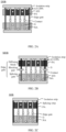
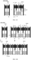
- the DDB standard cell includes a plurality of first gate strips G, two edge gates, a P-type active (P active, PA) region, and an N-type active (N active, NA) region.
- the edge gates and the first gate strips G are disposed at a same layer, and are located above the P-type active PA region and the N-type active NA region.
- the two edge gates are located on two sides of the plurality of first gate strips G. From a top view, the P-type active PA region and the N-type active NA region are located between the two edge gates.
- Contacts (contacts) are correspondingly provided on the first gate strips G, in the P-type active PA region, and in the N-type active NA region, and no contact is provided on the edge gates.
- the P-type active PA region, the N-type active NA region, the edge gates, and the first gate strips are located between two isolation strips (poly cuts).
- the MDB standard cell includes a plurality of first gate strips G, two edge gates, a P-type active PA region, and an N-type active NA region.
- the two edge gates are located on two sides of the plurality of first gate strips G, and the first gate strips G are located above the P-type active PA region and the N-type active NA region.
- the edge gate includes a diffusion break, a blocking gate, and a blocking part that separates the diffusion break and the blocking gate.
- the diffusion break runs through the P-type active PA region to perform a blocking function, and the blocking gate is located above the N-type active NA region.
- the P-type active PA region extends outwards the edge gate, an STI is disposed outside the N-type active NA region, a distance from an edge of the P-type active PA region to the edge gate is approximately 0.5 CPP, and a distance from an edge of the STI to the edge gate is approximately 0.5 CPP.
- a border of the MDB standard cell is at a location of 0.5 CPP outwards the edge gate, and the STI is disposed to reserve a spacing for blocking the N-type active NA region.
- the P-type active PA region When the border of the MDB standard cell is at the location of 0.5 CPP outwards the edge gate, the P-type active PA region is blocked by the diffusion break, and a P-type active PA region may be formed outside the diffusion break, to improve performance of the standard cell.
- the SDB standard cell includes a plurality of first gate strips G, two edge gates, a P-type active PA region, and an N-type active NA region.
- the two edge gates are located on two sides of the plurality of first gate strips G, and the first gate strips G are located above the P-type active PA region and the N-type active NA region.
- the edge gate is a diffusion break, runs through the P-type active PA region and the N-type active NA region, and the P-type active PA region and the N-type active NA region are located between the two edge gates.
- Contacts are correspondingly provided on the first gate strips G, in the P-type active PA region, and in the N-type active NAregion, and no contact is provided on the edge gates.
- the P-type active PAregion, the N-type active NA region, the edge gates, and the first gate strips are located between two isolation strips.
- a center line of the edge gate of the SDB standard cell is a border of the SDB standard cell.
- the P-type active PA region and the N-type active NA region are blocked by the diffusion break, and the border of the SDB standard cell does not need to extend outwards the edge gate. Therefore, left and right ends of the DDB standard cell and MDB standard cell each extend by about 0.5 CPP in comparison with left and right ends of the SDB standard cell.
- HP high performance
- HD high density
- an out-of-order execution module in a CPU core is used as an example.
- a performance, power consumption, area (performance power area, PPA) indicator comparison is performed between the module implemented based on the MDB standard cell and the module implemented based on the SDB standard cell.
- Physical synthesis implementations are compared under a condition in which a power supply voltage VDD is 0.6 V, a temperature is 85°C, and a typical corner (typical corner, TT) is TT 0 (namely, tt0p6v85c in Table 1) and a condition in which a power supply voltage VDD is 1.0 V, a temperature is 85°C, and a typical corner (typical corner, TT) is TT 1 (namely, tt1p0v85c in Table 1).
- a speed (speed) of the MDB standard cell is 2% to 8% higher than that of the SDB standard cell, but an area of the MDB standard cell is 5% to 12% larger than that of the SDB standard cell.
- Use of the MDB standard cell increases an area of a chip, resulting in an increase in costs of the chip.
- leakage (leakage) power consumption of the MDB standard cell is more than 25% higher than that of the SDB standard cell. For consumer products, the leakage power consumption is an important indicator, and an increase in the leakage power consumption is unacceptable.
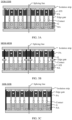
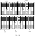
- the left and right ends of the MDB standard cell and the DDB standard cell each extend by about 0.5 CPP in comparison with the left and right ends of the SDB standard cell, as shown in FIG. 3A , when two DDB standard cells are spliced, a splicing line is located between edge gates of the two DDB standard cells, and a distance between the splicing line and the edge gate is approximately 0.5 CPP. As shown in FIG. 3B , when two MDB standard cells are spliced, a splicing line is located between edge gates of the two MDB standard cells, and a distance between the splicing line and the edge gate is approximately 0.5 CPP. As shown in FIG.
- an embodiment of this application provides a new DDB standard cell and MDB standard cell, so that standard cells of a same type can be spliced with each other, and different types of standard cells can also be spliced with each other.
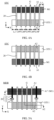
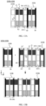
- an embodiment of this application provides a standard cell (standard cell) STC.
- the standard cell STC includes a first active region A1, a second active region A2, at least one first gate strip G, two second gate strips 20, two spacing regions M1, and two first shallow trench isolation regions STI 1 that are disposed on one side of a substrate (not shown in FIG. 4A ).
- FIG. 4A an example in which the standard cell includes a plurality of first gate strips G is used for illustration.
- the standard cell STC provided in this embodiment of this application may include a substrate, or may not include a substrate.
- an example in which the standard cell STC includes a substrate is used for illustration.
- the substrate is not marked in a top view, and a relative location relationship between the substrate, and the first active region A1 and the second active region A2 may be seen from a sectional view shown below.
- the N-type active region is formed by doping an N-type impurity in a semiconductor
- the P-type active region is formed by doping a P-type impurity in a semiconductor.
- the second direction X intersects with (for example, is perpendicular to) the first direction Y. That the first active region A1 and the second active region A2 are an N-type active region and a P-type active region for each other may be understood as that the first active region A1 is one of the N-type active region and the P-type active region, and the second active region A2 is the other of the N-type active region and the P-type active region.
- a first row is a P-type active region row
- a second row is an N-type active region row
- the first active region A1 is a P-type active region
- the second active region A2 is an N-type active region
- the second active region A2 is a P-type active region
- the first active region A1 is an N-type active region.
- the following uses an example in which the first active region A1 is a P-type active region and the second active region A2 is an N-type active region.
- the standard cell STC further includes at least one first fin and at least one second fin.
- the first fin and the second fin are not shown in FIG. 4A or FIG. 4B .
- the first fin is located above the first active region A1, the first fin extends to an edge of the standard cell STC in the second direction X, and a plurality of first fins are arranged in the first direction Y.
- the second fin is located above the second active region A2, the second fin extends to an edge of the standard cell STC in the second direction X, and a plurality of second fins are arranged in the first direction Y.
- the first gate strip G extends in the first direction Y, and is located above the first active region A1 and the second active region A2 (the first gate strip G is located on a side that is of the first fin and the second fin and that is away from the first active region A1 and the second active region A2).
- a projection of the first gate strip G on a plane on which the substrate is located overlaps a projection of the first active region A1 and a projection of the second active region A2 on the plane on which the substrate is located.
- the first gate strip G spans the first active region A1 and the second active region A2.
- the second gate strip 20 extends in the first direction Y, the two second gate strips 20 and the at least one first gate strip G are arranged in the second direction X, and the at least one first gate strip G is located between the two second gate strips 20.
- the two second gate strips 20 and the at least one first gate strip G are arranged at equal spacings in the second direction X.
- the spacing is, for example, a CPP.
- a spacing between the second gate strip 20 and the first gate strip G may be, for example, a distance between a middle line of the second gate strip 20 and a middle line of the first gate strip G.
- a spacing between two abutted first gate strips G may be, for example, a spacing between a middle line of one first gate strip G and a middle line of the other first gate strip G.
- two ends of the second active region A2 are located below the two second gate strips 20 (a side close to the substrate 10), and an end of the first active region A1 is flush with or approximately flush with an end of the second active region A2.
- the projections of the first active region A1 and the second active region A2 on the plane on which the substrate is located are located between projections of the two second gate strips 20 on the plane on which the substrate is located.
- the spacing region M1 is located on an extension line of the first active region A1, and the first active region A1 is located between the two spacing regions M1 in the second direction X.
- a border between the first active region A1 and the spacing region M1 may be, for example, located at the middle line (extending in the first direction Y) of the second gate strip 20.
- the second gate strip 20 cooperates with the spacing region M1 to break the first active region A1.
- the second gate strip 20 and the spacing region M1 are described in detail subsequently, and details are not described herein.
- the first shallow trench isolation region STI 1 1 is located on an extension line of the second active region A2, and the second active region A2 is located between the two first shallow trench isolation regions STI 1 in the second direction X.
- a border between the second active region A2 and the first shallow trench isolation region STI 1 1 may be, for example, located at the middle line (extending in the first direction Y) of the second gate strip 20.
- a width L1 of the spacing region M1 and a width L2 of the first shallow trench isolation region STI 1 1 are equal to the arrangement spacing (for example, the CPP) between the second gate strip 20 and the first gate strip G in the second direction X.
- the width L1 of the spacing region M1 may be, for example, a distance from an end of the spacing region M1 to the middle line of the second gate strip 20.
- the width L2 of the first shallow trench isolation region STI 1 1 may be, for example, a distance from an end of the first shallow trench isolation region STI 1 1 to the middle line of the second gate strip 20.
- a width of a part that is in the standard cell STC and that diffuses outwards the second gate strip 20 is set to CPP but not 0.5 CPP.
- the standard cell STC extends one CPP on one side in comparison with the conventional SDB standard cell, and each side of the standard cell STC diffuses one CPP outwards the second gate strip 20 in the second direction X.
- a distance between the splicing line and the second gate strip 20 is an integer multiple of CPP. Therefore, standard cells STCs of different types may be directly abutted (abutted) to implement mixed splicing of the standard cells STCs of different types.
- the standard cell STC may be classified into an MDB standard cell and a DDB standard cell.
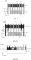
- the standard cell STC is an MDB standard cell. It can be learned with reference to FIG. 5A and FIG. 5B (a sectional view in a direction from A1 to A2 in FIG. 5A ), that a second gate strip 20 includes a first blocking gate 21, a first blocking part 22, and a first diffusion break (diffusion break) 23.
- the first diffusion break 23 extends to a bottom surface that is of the first active region A1 and that is close to the substrate 10.
- the first active region A1 and the spacing region M1 on two sides of the first diffusion break 23 are separated by the first diffusion break 23, and diffusion of the first active region A1 is blocked by the first diffusion break.
- the first blocking gate 21 is located on a side that is of the second active region A2 and that is away from the substrate 10.
- the first blocking gate 21 and the first gate strip G are disposed at a same layer (which are formed synchronously according to a same process).
- the second active region A2 and the first shallow trench isolation region STI 1 1 are not separated by the first blocking gate 21, the second active region A2 is in contact with the first shallow trench isolation region STI 1 1, and the first shallow trench isolation region STI 1 1 blocks diffusion of the second active region A2.
- the first blocking part 22 is of an axisymmetric structure, and a symmetry axis is the central line of the second gate strip 20.
- the first blocking part 22 may alternatively be in another shape.
- an insulation layer (for example, a SiO 2 layer) is further disposed on surfaces of the first active region A1 and the second active region A2, the insulation layer fills the first active region A1 and the second active region A2, and the second gate strip 20 is disposed on the insulation layer.
- the first active region A1 is a P-type active region
- the spacing region M1 is also a P-type active region
- the second active region A2 is an N-type active region
- the spacing region M2 is also an N-type active region.
- the standard cell STC is a DDB standard cell.
- the second gate strip 20 is located above the first active region A1 and the second active region A2 (on a side away from the substrate 10), and the spacing region M1 is a second shallow trench isolation region STI 2.
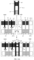
- the standard cell STC further includes two first splicing strips 30.
- the first splicing strip 30 extends in the first direction Y.
- the two second gate strips 20 and the at least one first gate strip G are located between the two first splicing strips 30 in the second direction X.
- the two first splicing strips 30, the two second gate strips 20, and the at least one first gate strip G are arranged at an equal interval.
- a distance between the first splicing strip 30 and the second gate strip 20 is equal to the arrangement spacing (for example, the CPP) between the second gate strip 20 and the first gate strip G in the second direction X.
- the first splicing strip 30 is a diffusion break, and the first splicing strips 30 extend to bottom surfaces of the spacing region M1 and the first shallow trench isolation region STI 1 1.
- the standard cell STC is an MDB standard cell
- the first splicing strip 30 and the first diffusion break 23 are disposed at a same layer.
- the first splicing strips 30 and the first gate strip G are disposed at a same layer.
- the first splicing strip 30 is disposed above the spacing region M1 and the first shallow trench isolation region STI 1 1 (on a side away from the substrate 10).
- the standard cell STC is a DDB standard cell, and the first splicing strips 30 and the first gate strip G are disposed at a same layer.
- the standard cell STC increases a width of two CPPs in the second direction X.
- the first active region A1 is a P-type active region
- the second active region A2 is an N-type active region
- a speed of the standard cell STC may be increased by about 8%
- leakage power consumption may be increased by about 30%.
- the standard cell STC is used together with the SDB standard cell, the standard cell STC is used on a time sequence critical path, and the SDB standard cell is used on a time sequence non-critical path, so that a design speed and energy efficiency can be improved under a same area and power consumption.
- the second active region A2 in the standard cell STC is a P-type active region
- the first active region A1 is an N-type active region
- the standard cell STC further includes two second splicing strips 40.
- the two first splicing strips 30, the two edge gates 20, and the at least one first gate strip G are all located between the two second splicing strips 40 in the second direction X.
- the two second splicing strips 40, the two first splicing strips 30, the two second gate strips 20, and the at least one first gate strip G are arranged at equal spacings. For example, a distance from the second splicing strip 40 to the first splicing strip 30 is equal to the arrangement spacing (for example, the CPP) between the second gate strip 20 and the first gate strip G in the second direction X.
- the second splicing strip 40 is a diffusion break, and second splicing strip 40 extends in the third direction Z to a plane on which bottom surfaces of the first active region A1 and the second active region A2 are located.
- the standard cell STC further includes two first extended active regions A1' and two second extended active regions A2' that are located on sides that are of the second splicing strips 40 and that face the first splicing strips 30.
- the first extended active region A1' is located on an extension line of the first active region A1, the first extended active region A1' is spliced with the spacing region M1, and the two spacing regions M1 are located between the two first extended active regions A1'.
- the second extended active region A2' is located on an extension line of the second active region A2, the second extended active region A2' is spliced with the first shallow trench isolation region STI 1 1, and the two first shallow trench isolation regions STI 1 are located between the two second extended active regions A2'.
- the first extended active region A1' and the first active region A1 are a same type of active regions, and the second extended active region A2' and the second active region A2 are a same type of active regions.
- first extended active region A1' and the first active region A1 are P-type active regions
- second extended active region A2' and the second active region A2 are N-type active regions.
- trench isolation structures are disposed at locations at which the first extended active region A1' and the two second extended active regions A2' are disposed.
- the second splicing strip 40 is added to the standard cell STC, a width of a single side of the standard cell STC is extended at least two CPPs outwards, and diffusion interrupt is implemented inside the standard cell STC.
- standard cells STCs may be directly abutted (abut), a spacing (spacing) of at least one CPP does not need to be reserved, and the standard cells STCs may be directly spliced.
- a quantity of extended gate strips G' between the first splicing strip 30 and the second splicing strip 40 on the left side is equal to a quantity of extended gate strips G' between the first splicing strip 30 and the second splicing strip 40 on the right side.
- FIG. 10B an example in which one extended gate strip G' is disposed between the first splicing strip 30 and the second splicing strip 40 is used for illustration.
- a plurality of extended gate strips G' may alternatively be disposed between the first splicing strip 30 and the second splicing strip 40, to adjust a layout arrangement of the standard cell STC.
- the second splicing strip 40, the extended gate strip G', the first splicing strip 30, the second gate strip 20, and the first gate strip G are arranged at equal spacings in the second direction X.
- the standard cell further includes a gate via (gate via, GV) and a source drain via (source drain via, SDV).
- GV gate via
- SDV source drain via
- the gate via GV communicates with the first gate strip G.
- a projection of the gate via GV on the plane on which the substrate is located overlaps a projection of the first gate strip G on the plane on which the substrate is located.
- a gate line is coupled to the first gate strip G through the gate via GV.
- a gate via GV is also correspondingly disposed above the extended gate strip G' (on a side away from the substrate 10).
- the extended gate strip G', the first fin, and the second fin form a transistor, to improve performance of the standard cell STC.
- the source drain via SDV located above the first active region A1 communicates with a part that is of the first fin and that is used as a source.
- a connection part M0 is disposed on a side that is of the plurality of first fins and that is away from the substrate, the connection part M0 is coupled to the plurality of first fins, and the source drain via SDV communicates with the connection part M0, so that the source drain via SDV communicates with the part that is of the first fin and that is used as the source.
- connection part M0 located above the first active region A1 (on the side away from the substrate 10) and the connection part M0 located above the second active region A2 (on the side away from the substrate 10) are insulated from each other, and the connection part M0 coupled to the source and the connection part M0 coupled to the drain are insulated from each other.
- the first fin, the second fin, the gate via GV, and the source drain via SDV in the standard cell STC are not illustrated.
- the isolation strip may non-disruptively extend from the second splicing strip 40 on the left side to the second splicing strip 40 on the right side.
- the isolation strip may disruptively extend from the second splicing strip 40 on the left side to the second splicing strip 40 on the right side, that is, the isolation strip may include a plurality of disruptive parts.
- FIG. 11C is merely an example, and does not impose any limitation.
- the standard cell STC may not include an isolation strip.
- the standard cell STC includes a plurality of first active regions A1 and a plurality of second active regions A2, and the active regions are arranged in a regular manner similar to the first active region A1, the second active region A2, the second active region A2, the first active region A1, the first active region A1, and the second active region A2.
- the standard cell STC provided in this embodiment of this application may be a standard cell having a logical function, or the standard cell STC may be a physical (physical) padding standard cell. This is not limited in this embodiment of this application.
- the standard cell STC in the standard cell library is optimized, so that the EDA obtains a better splicing solution when invoking the standard cell library, to optimize performance of a finally formed integrated circuit.
- the SDB standard cell is any SDB standard cell in the related technology, and the SDB standard cell and the MDB standard cell have a same height, or heights of the SDB standard cell and the MDB standard cell are in an integer multiple relationship.
- the SDB standard cell may be spliced with a DDB standard cell that does not include a first splicing strip 30.
- the SDB standard cell may alternatively be spliced with a DDB standard cell including a first splicing strip 30.
- the first splicing strip 30 overlaps the second diffusion break 50, regardless of whether the first splicing strip 30 and a first gate strip G are disposed at a same layer, or the first splicing strips 30 extend to bottom surfaces of the second shallow trench isolation region STI 2 and the first shallow trench isolation region STI 1 1.
- the second diffusion break 50 is one or more CPPs away from the second gate strip 20 of the DDB standard cell, and this meets a division rule of an isolation point in the EDA. Therefore, the DDB standard cell and the SDB standard cell can be spliced.
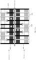
- an embodiment of this application provides an integrated circuit.
- the integrated circuit includes a first standard cell and a second standard cell.
- the first standard cell is any one of the foregoing MDB standard cells
- the second standard cell is any one of the foregoing DDB standard cells.
- the integrated circuit further includes two third diffusion breaks 60 disposed side by side, where the third diffusion break 60 extends in a first direction Y, and the two third diffusion breaks 60 are disposed side by side.
- the third diffusion breaks 60 extend to bottom surfaces of a spacing region M1 and a first shallow trench isolation region STI 1 1 in a third direction Z.
- the spacing region M1 of the MDB standard cell is disposed on a side that is of the third diffusion break 60 and that faces a second gate strip 20 of the MDB standard cell
- the spacing region M1 of the DDB standard cell is disposed on a side that is of the other third diffusion break 60 and that faces an edge gate 20 of the DDB standard cell.
- each of the MDB standard cell and the DDB standard cell includes a first splicing strip 30, and the first splicing strips 30 extend to bottom surfaces of the spacing region M1 and the first shallow trench isolation region STI 1 1.
- the first splicing strip 30 may be understood as a diffusion break.
- the MDB standard cell and the DDB standard cell may be spliced by using the first filler standard cell FL 1.
- the MDB standard cell and the DDB standard cell may alternatively be spliced by using another filler standard cell including the first splicing active region A1′′′ and the second splicing active region A2"'.
- the first splicing strip 30 (the first splicing strip 30 is used as the third diffusion break 60) or the third diffusion break 60 is finally retained at a splicing location.
- the first splicing active region A1′′′ and the second splicing active region A2′′′ are located between the first splicing strip 30 of the MDB standard cell and the first splicing strip 30 of the DDB standard cell, and the integrated circuit has one more first splicing strip 30 than the integrated circuit shown in FIG. 14A .
- each of the MDB standard cell and the DDB standard cell is a standard cell including a second splicing strip 40.
- the MDB standard cell and the DDB standard cell are allowed to be directly spliced by using the second splicing strip 40, and the second splicing strip 40 of the MDB standard cell and the second splicing strip 40 of the DDB standard cell overlap to form a structure shown in FIG. 14B .
- the first standard cell and the second standard cell are standard cells of a same type.
- an embodiment of this application further provides an integrated circuit.
- the integrated circuit includes a first standard cell and a second standard cell, and both the first standard cell and the second standard cell are MDB standard cells.
- the integrated circuit further includes two third diffusion breaks 60 disposed side by side, where the third diffusion break 60 extends in a first direction Y, and the two third diffusion breaks 60 are disposed side by side.
- the third diffusion breaks 60 extend to bottom surfaces of a spacing region M1 and a first shallow trench isolation region STI 1 1 in a third direction Z.
- the spacing region M1 of the MDB standard cell is disposed on a side that is of the third diffusion break 60 and that faces a second gate strip 20 of the MDB standard cell
- the spacing region M1 of the other MDB standard cell is disposed on a side that is of the other third diffusion break 60 and that faces an edge gate 20 of the MDB standard cell.
- the integrated circuit further includes a first splicing active region A1′′′ and a second splicing active region A2"'.
- the first splicing active region A1′′′ and the second splicing active region A2′′′ are located between the two third diffusion breaks 60.
- both the two MDB standard cells do not include a first splicing strip 30, and the two MDB standard cells may be spliced by using the first filler standard cell FL 1.
- splicing lines of the two MDB standard cells coincide with a middle line (a splicing line) of one third diffusion break 60 respectively, to form a structure shown in FIG. 15A .
- each of the two MDB standard cells includes a first splicing strip 30, and the first splicing strip 30 and the first gate strip G are disposed at a same layer.
- the two MDB standard cells may be spliced by using the first filler standard cell FL 1.
- the first splicing strip 30 coincides with the third diffusion break 60, the third diffusion break 60 is retained in the finally formed integrated circuit, and the integrated circuit has one more first splicing strip 30 than the integrated circuit shown in FIG. 15A .
- each of the two MDB standard cells includes a first splicing strip 30, and the first splicing strips 30 extend to bottom surfaces of the spacing region M1 and the first shallow trench isolation region STI 1 1.
- the two MDB standard cells may be spliced by using the first filler standard cell FL 1.
- the two MDB standard cells may alternatively be spliced by using another filler standard cell FL including the first filled active region A1′′′ and the second filled active region A2"'.
- the first splicing strip 30 (the first splicing strip 30 is used as the third diffusion break 60) or the third diffusion break 60 is finally retained at a splicing location.
- the first splicing active region A1′′′ and the second splicing active region A2′′′ are located between the first splicing strips 30 of the two MDB standard cells, and the integrated circuit has one more first splicing strip 30 than the integrated circuit shown in FIG. 15A .
- each of the two MDB standard cells is a standard cell including a second splicing strip 40.
- the two MDB standard cells are directly spliced by using the second splicing strip 40, and the second splicing strips 40 of the two MDB standard cells overlap, to form a structure shown in FIG. 15B .
- one of the two MDB standard cells includes a second splicing strip 40, and the other MDB standard cell does not include a second splicing strip 40.
- the first standard cell includes a second splicing strip 40
- the second standard cell does not include a second splicing strip 40.
- a middle line of the second splicing strip 40 is used as a splicing line of the first standard cell
- an edge line of the second standard cell is used as a splicing line of the second standard cell
- the first standard cell and the second standard cell are directly spliced at the splicing lines.
- the spacing region M1 and the first shallow trench isolation region STI 1 1 of the second standard cell are in contact with a side surface of the second splicing strip 40 in the first standard cell.
- the second standard cell may include a first splicing strip 30, or the second standard cell may not include a first splicing strip 30.
- an embodiment of this application further provides an integrated circuit.
- the integrated circuit includes a first standard cell and a second standard cell, and both the first standard cell and the second standard cell are DDB standard cells.
- a structure of the integrated circuit when both the first standard cell and the second standard cell are DDB standard cells is similar to a structure when both the first standard cell and the second standard cell are MDB standard cells, and only the MDB standard cell is replaced with the DDB standard cell.
- a structure of the second gate strip 20 and a structure of the spacing region M1 are replaced.
- the integrated circuit may further include an SDB standard cell and an MDB standard cell.
- a structure in FIG. 16 is merely an example, and does not impose any limitation.
Landscapes
- Design And Manufacture Of Integrated Circuits (AREA)
Applications Claiming Priority (2)
| Application Number | Priority Date | Filing Date | Title |
|---|---|---|---|
| CN202211147967.3A CN117727751B (zh) | 2022-09-19 | 2022-09-19 | 标准单元、集成电路、标准单元库及电子设备 |
| PCT/CN2023/102798 WO2024060747A1 (zh) | 2022-09-19 | 2023-06-27 | 标准单元、集成电路、标准单元库及电子设备 |
Publications (2)
| Publication Number | Publication Date |
|---|---|
| EP4579748A1 true EP4579748A1 (de) | 2025-07-02 |
| EP4579748A4 EP4579748A4 (de) | 2025-12-17 |
Family
ID=90202114
Family Applications (1)
| Application Number | Title | Priority Date | Filing Date |
|---|---|---|---|
| EP23867042.6A Pending EP4579748A4 (de) | 2022-09-19 | 2023-06-27 | Standardzelle, integrierte schaltung, standardzellenbibliothek und elektronische vorrichtung |
Country Status (4)
| Country | Link |
|---|---|
| US (1) | US20250221035A1 (de) |
| EP (1) | EP4579748A4 (de) |
| CN (1) | CN117727751B (de) |
| WO (1) | WO2024060747A1 (de) |
Families Citing this family (1)
| Publication number | Priority date | Publication date | Assignee | Title |
|---|---|---|---|---|
| CN121793764A (zh) * | 2024-09-29 | 2026-04-03 | 华为技术有限公司 | 芯片及电子设备 |
Family Cites Families (15)
| Publication number | Priority date | Publication date | Assignee | Title |
|---|---|---|---|---|
| KR102025309B1 (ko) * | 2013-08-22 | 2019-09-25 | 삼성전자 주식회사 | 반도체 장치 및 그 제조 방법 |
| US9831272B2 (en) * | 2016-03-31 | 2017-11-28 | Qualcomm Incorporated | Metal oxide semiconductor cell device architecture with mixed diffusion break isolation trenches |
| US10134734B2 (en) * | 2016-06-30 | 2018-11-20 | Qualcomm Incorporated | Fin field effect transistor (FET) (FinFET) complementary metal oxide semiconductor (CMOS) circuits employing single and double diffusion breaks for increased performance |
| KR102596528B1 (ko) * | 2018-01-15 | 2023-11-01 | 삼성전자주식회사 | 반도체 장치 |
| US10276554B1 (en) * | 2018-06-14 | 2019-04-30 | Taiwan Semiconductor Manufacturing Co., Ltd. | Integrated standard cell structure |
| KR102495912B1 (ko) * | 2018-08-10 | 2023-02-03 | 삼성전자 주식회사 | 표준 셀을 포함하는 집적 회로 및 이를 제조하기 위한 방법 |
| KR102599048B1 (ko) * | 2018-08-16 | 2023-11-06 | 삼성전자주식회사 | 표준 셀을 포함하는 집적 회로 및 이를 제조하기 위한 방법 |
| US10892322B2 (en) * | 2018-09-21 | 2021-01-12 | Qualcomm Incorporated | Circuits employing a double diffusion break (DDB) and single diffusion break (SDB) in different type diffusion region(s), and related fabrication methods |
| EP3867951A1 (de) * | 2018-11-07 | 2021-08-25 | Huawei Technologies Co., Ltd. | Integrierte schaltung und standardzelle dafür |
| US20200176330A1 (en) * | 2018-11-29 | 2020-06-04 | Qualcomm Incorporated | A structure and method for complementary metal oxide semiconductor (cmos) isolation |
| US11646305B2 (en) * | 2019-10-02 | 2023-05-09 | Samsung Electronics Co., Ltd. | Semiconductor devices and methods of manufacturing the same |
| US11810920B2 (en) * | 2019-11-29 | 2023-11-07 | Samsung Electronics Co., Ltd. | Integrated circuits including integrated standard cell structure |
| WO2022056412A1 (en) * | 2020-09-14 | 2022-03-17 | Synopsys, Inc. | Mixed diffusion break for cell design |
| US12191310B2 (en) * | 2021-01-11 | 2025-01-07 | Mediatek Inc. | Logic cell with small cell delay |
| KR102934456B1 (ko) * | 2021-01-21 | 2026-03-09 | 삼성전자주식회사 | 반도체 소자의 레이아웃 설계 방법 및 이를 이용한 반도체 소자의 제조 방법 |
-
2022
- 2022-09-19 CN CN202211147967.3A patent/CN117727751B/zh active Active
-
2023
- 2023-06-27 EP EP23867042.6A patent/EP4579748A4/de active Pending
- 2023-06-27 WO PCT/CN2023/102798 patent/WO2024060747A1/zh not_active Ceased
-
2025
- 2025-03-18 US US19/082,879 patent/US20250221035A1/en active Pending
Also Published As
| Publication number | Publication date |
|---|---|
| CN117727751A (zh) | 2024-03-19 |
| EP4579748A4 (de) | 2025-12-17 |
| CN117727751B (zh) | 2026-01-27 |
| US20250221035A1 (en) | 2025-07-03 |
| WO2024060747A1 (zh) | 2024-03-28 |
Similar Documents
| Publication | Publication Date | Title |
|---|---|---|
| TWI550777B (zh) | 靜態隨機存取記憶體單元以及靜態隨機存取記憶體單元陣列 | |
| US20250221035A1 (en) | Standard cell, integrated circuit, standard cell library, and electronic device | |
| US20220392999A1 (en) | Semiconductor integrated circuit device | |
| US20150161314A1 (en) | Layout design system and semiconductor device fabricated using the system | |
| US12232308B2 (en) | Semiconductor storage device | |
| US9659130B2 (en) | Layout design system for generating layout design of semiconductor device | |
| CN116153924A (zh) | 零扩散隔断 | |
| US20240292657A1 (en) | Display substrate and display device | |
| WO2024060746A1 (zh) | 标准单元及拼接方法、集成电路、标准单元库、电子设备 | |
| US20240403529A1 (en) | Zero diffusion break between standard cells using three-dimensional cross field effect self-aligned transistors | |
| CN212303671U (zh) | 设置有漏流导出结构的有机发光显示装置 | |
| CN120224700A (zh) | 封装衬底中的垂直嵌入式部件 | |
| US20240008240A1 (en) | Semiconductor structure and manufacturing method thereof | |
| WO2024113775A9 (zh) | 集成电路及电子设备 | |
| CN114005862B (zh) | 阵列基板、显示面板及显示装置 | |
| JP2024517175A (ja) | 三次元メモリ、チップパッケージ構造、および電子デバイス | |
| CN115413370A (zh) | 显示基板及显示装置 | |
| CN121262823B (zh) | 静态随机存取存储器结构及其制备方法 | |
| US20250259940A1 (en) | Parallel lines formed by isolation cut | |
| CN113707661A (zh) | 静态随机存取存储器 | |
| US20250359245A1 (en) | Semiconductor layout with dummy patterns and method of manufacturing the same | |
| CN115424524B (zh) | 显示面板和显示装置 | |
| US20240282778A1 (en) | Display substrate, method for manufacturing same, and display device | |
| EP4495999A2 (de) | Zellenarchitektur einer halbleitervorrichtung mit auf der basis eines rückseitigen stromverteilungsnetzes verbundenen halbleiterzellen | |
| US20240324192A1 (en) | One-time programmable memory device |
Legal Events
| Date | Code | Title | Description |
|---|---|---|---|
| STAA | Information on the status of an ep patent application or granted ep patent |
Free format text: STATUS: THE INTERNATIONAL PUBLICATION HAS BEEN MADE |
|
| PUAI | Public reference made under article 153(3) epc to a published international application that has entered the european phase |
Free format text: ORIGINAL CODE: 0009012 |
|
| STAA | Information on the status of an ep patent application or granted ep patent |
Free format text: STATUS: REQUEST FOR EXAMINATION WAS MADE |
|
| 17P | Request for examination filed |
Effective date: 20250324 |
|
| AK | Designated contracting states |
Kind code of ref document: A1 Designated state(s): AL AT BE BG CH CY CZ DE DK EE ES FI FR GB GR HR HU IE IS IT LI LT LU LV MC ME MK MT NL NO PL PT RO RS SE SI SK SM TR |
|
| REG | Reference to a national code |
Ref country code: DE Ref legal event code: R079 Free format text: PREVIOUS MAIN CLASS: H01L0027020000 Ipc: H10D0089100000 |
|
| A4 | Supplementary search report drawn up and despatched |
Effective date: 20251119 |
|
| RIC1 | Information provided on ipc code assigned before grant |
Ipc: H10D 89/10 20250101AFI20251113BHEP Ipc: G06F 30/392 20200101ALI20251113BHEP Ipc: H10D 84/90 20250101ALI20251113BHEP Ipc: H10D 84/01 20250101ALN20251113BHEP Ipc: H10D 84/85 20250101ALN20251113BHEP |
|
| DAV | Request for validation of the european patent (deleted) | ||
| DAX | Request for extension of the european patent (deleted) |