EP4579737A1 - Semiconductor power module, motor controller, and vehicle - Google Patents
Semiconductor power module, motor controller, and vehicle Download PDFInfo
- Publication number
- EP4579737A1 EP4579737A1 EP23859025.1A EP23859025A EP4579737A1 EP 4579737 A1 EP4579737 A1 EP 4579737A1 EP 23859025 A EP23859025 A EP 23859025A EP 4579737 A1 EP4579737 A1 EP 4579737A1
- Authority
- EP
- European Patent Office
- Prior art keywords
- transverse section
- conductive region
- section
- power module
- vertical section
- Prior art date
- Legal status (The legal status is an assumption and is not a legal conclusion. Google has not performed a legal analysis and makes no representation as to the accuracy of the status listed.)
- Pending
Links
Images


Classifications
-
- H—ELECTRICITY
- H10—SEMICONDUCTOR DEVICES; ELECTRIC SOLID-STATE DEVICES NOT OTHERWISE PROVIDED FOR
- H10W—GENERIC PACKAGES, INTERCONNECTIONS, CONNECTORS OR OTHER CONSTRUCTIONAL DETAILS OF DEVICES COVERED BY CLASS H10
- H10W40/00—Arrangements for thermal protection or thermal control
-
- H—ELECTRICITY
- H10—SEMICONDUCTOR DEVICES; ELECTRIC SOLID-STATE DEVICES NOT OTHERWISE PROVIDED FOR
- H10W—GENERIC PACKAGES, INTERCONNECTIONS, CONNECTORS OR OTHER CONSTRUCTIONAL DETAILS OF DEVICES COVERED BY CLASS H10
- H10W44/00—Electrical arrangements for controlling or matching impedance
-
- H—ELECTRICITY
- H10—SEMICONDUCTOR DEVICES; ELECTRIC SOLID-STATE DEVICES NOT OTHERWISE PROVIDED FOR
- H10W—GENERIC PACKAGES, INTERCONNECTIONS, CONNECTORS OR OTHER CONSTRUCTIONAL DETAILS OF DEVICES COVERED BY CLASS H10
- H10W44/00—Electrical arrangements for controlling or matching impedance
- H10W44/501—Inductive arrangements
-
- H—ELECTRICITY
- H10—SEMICONDUCTOR DEVICES; ELECTRIC SOLID-STATE DEVICES NOT OTHERWISE PROVIDED FOR
- H10W—GENERIC PACKAGES, INTERCONNECTIONS, CONNECTORS OR OTHER CONSTRUCTIONAL DETAILS OF DEVICES COVERED BY CLASS H10
- H10W70/00—Package substrates; Interposers; Redistribution layers [RDL]
- H10W70/40—Leadframes
- H10W70/461—Leadframes specially adapted for cooling
-
- H—ELECTRICITY
- H10—SEMICONDUCTOR DEVICES; ELECTRIC SOLID-STATE DEVICES NOT OTHERWISE PROVIDED FOR
- H10W—GENERIC PACKAGES, INTERCONNECTIONS, CONNECTORS OR OTHER CONSTRUCTIONAL DETAILS OF DEVICES COVERED BY CLASS H10
- H10W70/00—Package substrates; Interposers; Redistribution layers [RDL]
- H10W70/40—Leadframes
- H10W70/476—Oscillators in combination with leadframes
-
- H—ELECTRICITY
- H10—SEMICONDUCTOR DEVICES; ELECTRIC SOLID-STATE DEVICES NOT OTHERWISE PROVIDED FOR
- H10W—GENERIC PACKAGES, INTERCONNECTIONS, CONNECTORS OR OTHER CONSTRUCTIONAL DETAILS OF DEVICES COVERED BY CLASS H10
- H10W70/00—Package substrates; Interposers; Redistribution layers [RDL]
- H10W70/60—Insulating or insulated package substrates; Interposers; Redistribution layers
-
- H—ELECTRICITY
- H10—SEMICONDUCTOR DEVICES; ELECTRIC SOLID-STATE DEVICES NOT OTHERWISE PROVIDED FOR
- H10W—GENERIC PACKAGES, INTERCONNECTIONS, CONNECTORS OR OTHER CONSTRUCTIONAL DETAILS OF DEVICES COVERED BY CLASS H10
- H10W70/00—Package substrates; Interposers; Redistribution layers [RDL]
- H10W70/60—Insulating or insulated package substrates; Interposers; Redistribution layers
- H10W70/611—Insulating or insulated package substrates; Interposers; Redistribution layers for connecting multiple chips together
-
- H—ELECTRICITY
- H10—SEMICONDUCTOR DEVICES; ELECTRIC SOLID-STATE DEVICES NOT OTHERWISE PROVIDED FOR
- H10W—GENERIC PACKAGES, INTERCONNECTIONS, CONNECTORS OR OTHER CONSTRUCTIONAL DETAILS OF DEVICES COVERED BY CLASS H10
- H10W70/00—Package substrates; Interposers; Redistribution layers [RDL]
- H10W70/60—Insulating or insulated package substrates; Interposers; Redistribution layers
- H10W70/62—Insulating or insulated package substrates; Interposers; Redistribution layers characterised by their interconnections
- H10W70/65—Shapes or dispositions of interconnections
-
- H—ELECTRICITY
- H10—SEMICONDUCTOR DEVICES; ELECTRIC SOLID-STATE DEVICES NOT OTHERWISE PROVIDED FOR
- H10W—GENERIC PACKAGES, INTERCONNECTIONS, CONNECTORS OR OTHER CONSTRUCTIONAL DETAILS OF DEVICES COVERED BY CLASS H10
- H10W70/00—Package substrates; Interposers; Redistribution layers [RDL]
- H10W70/60—Insulating or insulated package substrates; Interposers; Redistribution layers
- H10W70/62—Insulating or insulated package substrates; Interposers; Redistribution layers characterised by their interconnections
- H10W70/65—Shapes or dispositions of interconnections
- H10W70/658—Shapes or dispositions of interconnections for devices provided for in groups H10D8/00 - H10D48/00
-
- H—ELECTRICITY
- H10—SEMICONDUCTOR DEVICES; ELECTRIC SOLID-STATE DEVICES NOT OTHERWISE PROVIDED FOR
- H10W—GENERIC PACKAGES, INTERCONNECTIONS, CONNECTORS OR OTHER CONSTRUCTIONAL DETAILS OF DEVICES COVERED BY CLASS H10
- H10W90/00—Package configurations
-
- H—ELECTRICITY
- H10—SEMICONDUCTOR DEVICES; ELECTRIC SOLID-STATE DEVICES NOT OTHERWISE PROVIDED FOR
- H10W—GENERIC PACKAGES, INTERCONNECTIONS, CONNECTORS OR OTHER CONSTRUCTIONAL DETAILS OF DEVICES COVERED BY CLASS H10
- H10W90/00—Package configurations
- H10W90/10—Configurations of laterally-adjacent chips
-
- H—ELECTRICITY
- H10—SEMICONDUCTOR DEVICES; ELECTRIC SOLID-STATE DEVICES NOT OTHERWISE PROVIDED FOR
- H10W—GENERIC PACKAGES, INTERCONNECTIONS, CONNECTORS OR OTHER CONSTRUCTIONAL DETAILS OF DEVICES COVERED BY CLASS H10
- H10W72/00—Interconnections or connectors in packages
- H10W72/50—Bond wires
- H10W72/541—Dispositions of bond wires
- H10W72/547—Dispositions of multiple bond wires
- H10W72/5475—Dispositions of multiple bond wires multiple bond wires connected to common bond pads at both ends of the wires
-
- H—ELECTRICITY
- H10—SEMICONDUCTOR DEVICES; ELECTRIC SOLID-STATE DEVICES NOT OTHERWISE PROVIDED FOR
- H10W—GENERIC PACKAGES, INTERCONNECTIONS, CONNECTORS OR OTHER CONSTRUCTIONAL DETAILS OF DEVICES COVERED BY CLASS H10
- H10W72/00—Interconnections or connectors in packages
- H10W72/50—Bond wires
- H10W72/551—Materials of bond wires
-
- H—ELECTRICITY
- H10—SEMICONDUCTOR DEVICES; ELECTRIC SOLID-STATE DEVICES NOT OTHERWISE PROVIDED FOR
- H10W—GENERIC PACKAGES, INTERCONNECTIONS, CONNECTORS OR OTHER CONSTRUCTIONAL DETAILS OF DEVICES COVERED BY CLASS H10
- H10W72/00—Interconnections or connectors in packages
- H10W72/851—Dispositions of multiple connectors or interconnections
- H10W72/874—On different surfaces
- H10W72/884—Die-attach connectors and bond wires
-
- H—ELECTRICITY
- H10—SEMICONDUCTOR DEVICES; ELECTRIC SOLID-STATE DEVICES NOT OTHERWISE PROVIDED FOR
- H10W—GENERIC PACKAGES, INTERCONNECTIONS, CONNECTORS OR OTHER CONSTRUCTIONAL DETAILS OF DEVICES COVERED BY CLASS H10
- H10W90/00—Package configurations
- H10W90/701—Package configurations characterised by the relative positions of pads or connectors relative to package parts
- H10W90/731—Package configurations characterised by the relative positions of pads or connectors relative to package parts of die-attach connectors
- H10W90/734—Package configurations characterised by the relative positions of pads or connectors relative to package parts of die-attach connectors between a chip and a stacked insulating package substrate, interposer or RDL
-
- H—ELECTRICITY
- H10—SEMICONDUCTOR DEVICES; ELECTRIC SOLID-STATE DEVICES NOT OTHERWISE PROVIDED FOR
- H10W—GENERIC PACKAGES, INTERCONNECTIONS, CONNECTORS OR OTHER CONSTRUCTIONAL DETAILS OF DEVICES COVERED BY CLASS H10
- H10W90/00—Package configurations
- H10W90/701—Package configurations characterised by the relative positions of pads or connectors relative to package parts
- H10W90/751—Package configurations characterised by the relative positions of pads or connectors relative to package parts of bond wires
- H10W90/754—Package configurations characterised by the relative positions of pads or connectors relative to package parts of bond wires between a chip and a stacked insulating package substrate, interposer or RDL
Definitions
- the semiconductor power module is usually used in an inverter to convert an alternating current into a direct current, or convert a direct current into an alternating current.
- the semiconductor power module has advantages such as high integration and a small volume.
- a voltage generated by a stray inductance of a loop during switching of a semiconductor chip is excessively large, and electromagnetic interference is generated due to damped oscillation, which increases a switching loss.
- a high current is to be output, multiple chips need to be connected in parallel, and thus a region occupied by the chips is large, and an inductance is also increased accordingly.
- the present disclosure further provides a motor controller having the foregoing semiconductor power module.
- the present disclosure further provides a vehicle having the foregoing motor controller.
- a first aspect of an embodiment according to the present disclosure provides a semiconductor power module, including: a substrate, the substrate having a first direction and a second direction orthogonal to each other; a first conductive region and a second conductive region that are spaced apart on the substrate, the first conductive region including a first transverse section and a second transverse section, the second conductive region including a third transverse section and a fourth transverse section, and the first transverse section, the third transverse section, the second transverse section, and the fourth transverse section being sequentially arranged in the first direction, where the first conductive region and the second conductive region are configured to transmit DC signals; and at least one first power chip and at least one second power chip, the first power chip being respectively connected to the first transverse section and the third transverse section, and the second power chip being respectively connected to the second transverse section and the fourth transverse section.
- the semiconductor power module according to this embodiment of the present disclosure has advantages such as a small stray inductance and a good heat dissipation effect.
- the first conductive region further includes a first vertical section, the first transverse section and the second transverse section both extend in the second direction, the first vertical section extends in the first direction, and two ends of the first vertical section are respectively connected to the first transverse section and the second transverse section.
- the second conductive region further includes a second vertical section, the third transverse section and the fourth transverse section both extend in the second direction, the second vertical section extends in the first direction, and two ends of the second vertical section are respectively connected to the third transverse section and the fourth transverse section.
- the first vertical section and the second vertical section are respectively arranged adjacent to two opposite sides of the substrate in the second direction.
- the semiconductor power module 1 in this embodiment of the present disclosure has a small stray inductance, a low temperature at a position of the power chip, and a very good heat dissipation effect, which is conducive to applying the semiconductor power module 1 to a circuit with a high switching speed.
- the first conductive region 110 further includes a first vertical section 113.
- the first transverse section 111 and the second transverse section 112 both extend in the second direction, the first vertical section 113 extends in the first direction, and two ends of the first vertical section 113 are respectively connected to the first transverse section 111 and the second transverse section 112.
- the second conductive region 120 further includes a second vertical section 123.
- the third transverse section 121 and the fourth transverse section 122 both extend in the second direction, the second vertical section 123 extends in the first direction, and two ends of the second vertical section 123 are respectively connected to the third transverse section 121 and the fourth transverse section 122.
- the first vertical section 113 and the second vertical section 123 are respectively arranged adjacent to two opposite sides of the substrate 100 in the second direction.
- the first conductive region 110 forms a "U"-shaped structure
- the second conductive region 120 forms a "U"-shaped structure.
- the first conductive region 110 is inserted into the second conductive region 120 from an opening of the second conductive region 120
- the second conductive region 120 is inserted into the first conductive region 110 from an opening of the first conductive region 110.
- first transverse section 111 and the second transverse section 112 are connected in series through the first vertical section 113, and the third transverse section 121 and the fourth transverse section 122 are connected in series through the second vertical section 123, so that the first power chip 200 and the second power chip 300 can be connected in series, and the first conductive region 110 and the second conductive region 120 occupy less space as a whole.
- one end of the first vertical section 113 is flush with a side of the first transverse section 111 that faces away from the second transverse section 112, and the other end of the first vertical section 113 is flush with a side of the second transverse section 112 that faces away from the first transverse section 111; one end of the second vertical section 123 is flush with a side of the third transverse section 121 that faces away from the fourth transverse section 122, and the other end of the second vertical section 123 is flush with a side of the fourth transverse section 122 that faces away from the third transverse section 121.
- a sum of sizes of the first vertical section 113 and the fourth transverse section 122 in the first direction is equal to a sum of sizes of the second vertical section 123 and the first transverse section 111 in the first direction.
- the first conductive region 110 and the second conductive region 120 occupy less space as a whole in the first direction, and the first power chip 200 and the second power chip 300 are distributed more evenly in the first direction.
- a side of the first vertical section 113 that faces away from the second vertical section 123 is flush with an end of the fourth transverse section 122 away from the second vertical section 123, and a side of the second vertical section 123 that faces away from the first vertical section 113 is flush with a side of the first transverse section 111 away from the first vertical section 113.
- a length of the first transverse section 111 may be the same as a length of the fourth transverse section 122
- a length of the second transverse section 112 may be the same as a length of the third transverse section 121
- a sum of sizes of the second transverse section 112 and the second vertical section 123 in the second direction is substantially equal to the length of the first transverse section 111
- a sum of sizes of the third transverse section 121 and the first vertical section 113 in the second direction is substantially equal to the length of the fourth transverse section 122.
- the first high-voltage connection part 710 is arranged at an end of the third vertical section 131 away from the fifth transverse section 133.
- a size of the first high-voltage connection part 710 in the second direction is greater than a width of the third vertical section 131 and greater than a width of the second DC transmission terminal 700.
- the second DC transmission terminal 700 is connected to the first high-voltage connection part 710.
- a width of the third vertical section 131 is less than a width of the second DC transmission terminal 700, so that a size of the semiconductor power module 1 in the second direction is reduced, thereby facilitating miniaturization of the semiconductor power module 1.
- the third vertical section 131 can be connected to the second DC transmission terminal 700, and in addition, the second DC transmission terminal 700 does not extend beyond the first high-voltage connection part 710 in the second direction, so that a contact area between the second DC transmission terminal 700 and the third vertical section 131 is improved, thereby ensuring reliability of an electrical connection between the second DC transmission terminal 700 and the third vertical section 131.
- the second high-voltage connection part 810 is arranged at an end of the fourth vertical section 132 away from the fifth transverse section 133.
- a size of the second high-voltage connection part 810 in the second direction is greater than a width of the fourth vertical section 132 and greater than a width of the third DC transmission terminal 800, and the third DC transmission terminal 800 is connected to the second high-voltage connection part 810.
- a width of the fourth vertical section 132 is less than a width of the third DC transmission terminal 800, so that a size of the semiconductor power module 1 in the second direction is reduced, thereby facilitating miniaturization of the semiconductor power module 1.
- the fourth vertical section 132 can be connected to the third DC transmission terminal 800, and in addition, the third DC transmission terminal 800 does not extend beyond the second high-voltage connection part 810 in the second direction, so that a contact area between the third DC transmission terminal 800 and the fourth vertical section 132 is improved, thereby ensuring reliability of an electrical connection between the third DC transmission terminal 800 and the fourth vertical section 132.
- the first high-voltage connection part 710 and the second high-voltage connection part 810 are located on two opposite sides of the low-voltage connection part 610 in the second direction.
- the low-voltage connection part 610 can avoid the first high-voltage connection part 710 and the second high-voltage connection part 810.
- a size of the semiconductor power module 1 in the second direction is prevented from increasing, thereby facilitating miniaturization of the semiconductor power module 1.
- the first transverse section 111 can be connected to the low-voltage connection part 610, and in addition, the low-voltage connection part 610 does not extend beyond the first transverse section 111 in the second direction, thereby ensuring reliability of an electrical connection between the first DC transmission terminal 600 and the first transverse section 111.
- a width of the second DC transmission terminal 700 is the same as a width of the third DC transmission terminal 800 and is less than a width of the first DC transmission terminal 600. Because the second DC transmission terminal 700 and the third DC transmission terminal 800 are both connected to the third conductive region 130, the width of the first DC transmission terminal 600 may be substantially equal to a sum of the width of the second DC transmission terminal 700 and the width of the third DC transmission terminal 800, to ensure that a direct current input impedance is substantially the same as a direct current output impedance, thereby reducing heat generation of the semiconductor power module 1.
- the substrate 100 includes an insulation layer 101, a circuit layer 102, and a heat dissipation layer 103.
- the circuit layer 102 is connected to a side of the insulation layer 101 in a thickness direction
- the first conductive region 110 and the second conductive region 120 are formed on the circuit layer 102
- the heat dissipation layer 103 is connected to the other side of the insulation layer 101 in the thickness direction.
- the insulation layer 101 may be made of ceramic, for example, made of aluminum oxide (Al2O3), aluminum nitride (AlN), and silicon nitride (Si3N4). In this way, the insulation layer 101 has a good heat conduction effect, a strong insulation capability, and a stable chemical property, which may not only isolate a connection between the conductive layer and the heat dissipation layer 103, but also provide a heat dissipation channel for the semiconductor power module 1.
- Al2O3 aluminum oxide
- AlN aluminum nitride
- Si3N4 silicon nitride
- the circuit layer 102 may be made of a copper material, and the copper is etched into the first conductive region 110, the second conductive region 120, the third conductive region 130, and the fourth conductive region 140.
- the heat dissipation layer 103 may be made of a copper material, and the first DC transmission terminal 600, the second DC transmission terminal 700, the third DC transmission terminal 800, and the AC transmission terminal 900 may all be made of copper materials. In this way, the circuit layer 102, the heat dissipation layer 103, the first DC transmission terminal 600, the second DC transmission terminal 700, the third DC transmission terminal 800, and the AC transmission terminal 900 all have good conductivity performance and heat dissipation performance, and can be effectively connected to an external device.
- the semiconductor power module 1 further includes an insulation cover 1100.
- the insulation cover 1100 is mounted on the substrate 100 and covers the first conductive region 110, the second conductive region 120, the first power chip 200, and the second power chip 300.
- the insulation cover 1100 may insulate and protect a device, thereby improving safety of an electrical connection of the semiconductor power module 1.
- the motor controller 2 includes a heat dissipation bottom plate 104, a coolant channel 1200, and the semiconductor power module 1 according to the foregoing embodiments of the present disclosure.
- the heat dissipation bottom plate 104 is mounted in the coolant channel 1200, and the semiconductor power module 1 is arranged on the heat dissipation bottom plate 104.
- each semiconductor power module 1 there are multiple semiconductor power modules 1 and are arranged on the heat dissipation bottom plate 104 in the second direction, and the multiple semiconductor power modules 1 may be arranged in parallel.
- a bottom of each semiconductor power module 1 is welded to the heat dissipation bottom plate 104.
- the coolant channel 1200 may be an open-groove water channel, and the heat dissipation bottom plate 104 is mounted on the open groove of the coolant channel 1200, so that a heat dissipation function for the semiconductor power module 1 is implemented. This design process is simple, easy to implement, and convenient to operate.
- the semiconductor power module 1 provided based on the foregoing embodiments has a uniform structural layout and a good heat dissipation effect, and the motor controller 2 can be used in various coolant channel applications, such as a series coolant channel or a parallel coolant channel, so that application flexibility of the motor controller 2 is improved, and a stray inductance in a loop during application is reduced.
- the motor controller 2 has advantages such as a small stray inductance and a good heat dissipation effect.
- a vehicle 1000 according to an embodiment of the present disclosure is described below with reference to FIG. 11 .
- the vehicle 1000 includes a motor 1001 and the motor controller 2 according to the foregoing embodiment of the present disclosure.
- the motor controller 2 is connected to the motor 1001.
- the vehicle according to the embodiment of the present disclosure has advantages such as a small stray inductance and a good heat dissipation effect.
Landscapes
- Inverter Devices (AREA)
Abstract
Description
- The present disclosure claims priority to and benefits of
Chinese Patent Application No. 202211058483.1, filed on August 31, 2022 - The present disclosure relates to the field of semiconductor technologies, and in particular, to a semiconductor power module, a motor controller, and a vehicle.
- Semiconductor power modules are widely used in industry. The semiconductor power module is usually used in an inverter to convert an alternating current into a direct current, or convert a direct current into an alternating current. The semiconductor power module has advantages such as high integration and a small volume. However, in an inversion process, a voltage generated by a stray inductance of a loop during switching of a semiconductor chip is excessively large, and electromagnetic interference is generated due to damped oscillation, which increases a switching loss. In addition, if a high current is to be output, multiple chips need to be connected in parallel, and thus a region occupied by the chips is large, and an inductance is also increased accordingly.
- The present disclosure aims to resolve at least one of the technical problems in the prior art. Therefore, an objective of the present disclosure is to provide a semiconductor power module. The semiconductor power module has advantages such as a small stray inductance and a good heat dissipation effect.
- The present disclosure further provides a motor controller having the foregoing semiconductor power module.
- The present disclosure further provides a vehicle having the foregoing motor controller.
- To achieve the foregoing objective, a first aspect of an embodiment according to the present disclosure provides a semiconductor power module, including: a substrate, the substrate having a first direction and a second direction orthogonal to each other; a first conductive region and a second conductive region that are spaced apart on the substrate, the first conductive region including a first transverse section and a second transverse section, the second conductive region including a third transverse section and a fourth transverse section, and the first transverse section, the third transverse section, the second transverse section, and the fourth transverse section being sequentially arranged in the first direction, where the first conductive region and the second conductive region are configured to transmit DC signals; and at least one first power chip and at least one second power chip, the first power chip being respectively connected to the first transverse section and the third transverse section, and the second power chip being respectively connected to the second transverse section and the fourth transverse section.
- The semiconductor power module according to this embodiment of the present disclosure has advantages such as a small stray inductance and a good heat dissipation effect.
- According to some embodiments of the present disclosure, the first conductive region further includes a first vertical section, the first transverse section and the second transverse section both extend in the second direction, the first vertical section extends in the first direction, and two ends of the first vertical section are respectively connected to the first transverse section and the second transverse section. The second conductive region further includes a second vertical section, the third transverse section and the fourth transverse section both extend in the second direction, the second vertical section extends in the first direction, and two ends of the second vertical section are respectively connected to the third transverse section and the fourth transverse section. The first vertical section and the second vertical section are respectively arranged adjacent to two opposite sides of the substrate in the second direction.
- According to some embodiments of the present disclosure, an end of the first vertical section is flush with the second transverse section, a back side of the first transverse section, and the other end of the first vertical section is flush with the first transverse section, a back side of the second transverse section; and one end of the second vertical section is flush with the fourth transverse section, a back side of the third transverse section, and the other end of the second vertical section is flush with the third transverse section, a back side of the fourth transverse section.
- According to some embodiments of the present disclosure, a side of the first vertical section that faces away from the second vertical section is flush with an end of the fourth transverse section away from the second vertical section; and a side of the second vertical section that faces away from the first vertical section is flush with a side of the first transverse section away from the first vertical section.
- According to some embodiments of the present disclosure, the first power chip is mounted on the third transverse section, and the first power chip is connected to the first transverse section through a first connection member.
- According to some embodiments of the present disclosure, the second power chip is mounted on the fourth transverse section, and the second power chip is connected to the second transverse section through a second connection member.
- According to some embodiments of the present disclosure, the semiconductor power module includes: a third conductive region. The third conductive region is arranged on the substrate and spaced apart from the first conductive region and the second conductive region, and the third conductive region is constructed in a closed loop shape arranged around the first conductive region and the second conductive region.
- According to some embodiments of the present disclosure, the third conductive region includes a third vertical section, a fourth vertical section, a fifth transverse section, and a sixth transverse section. The third vertical section and the fourth vertical section extend in the first direction and are spaced apart in the second direction; the fifth transverse section and the sixth transverse section extend in the second direction and are spaced apart in the first direction; the third vertical section, the fifth transverse section, the fourth vertical section, and the sixth transverse section are sequentially connected end to end; and the first conductive region and the second conductive region are located between the third vertical section and the fourth vertical section in the second direction; the fifth transverse section is located on the side of the fourth transverse section that faces away from the third transverse section in the first direction, where the third conductive region is configured to transmit DC signals. The semiconductor power module includes: at least one third power chip and at least one fourth power chip. The third power chip is arranged on the fifth transverse section, the third power chip is connected to the fourth transverse section, the fourth power chip is arranged on the fifth transverse section, and the fourth power chip is connected to the fourth transverse section.
- According to some embodiments of the present disclosure, multiple third power chips are included, the multiple third power chips are spaced apart in the second direction, and the multiple third power chips are arranged in a row in the second direction. Multiple fourth power chips are included, the multiple fourth power chips are spaced apart in the second direction, and the multiple fourth power chips are arranged in a row in the second direction. The row in which the third power chips are located and the row in which the fourth power chips are located are spaced apart in the first direction. A sum of a quantity of first power chips and a quantity of second power chips is equal to a sum of a quantity of the third power chips and a quantity of the fourth power chips.
- According to some embodiments of the present disclosure, the multiple third power chips and the multiple fourth power chips are alternately arranged in the second direction.
- According to some embodiments of the present disclosure, the semiconductor power module includes: a fourth conductive region. The fourth conductive region is arranged on the substrate and is spaced apart from the first conductive region, the second conductive region, and the third conductive region. The fourth conductive region extends in the second direction and is located on a side of the fifth transverse section that faces away from the fourth transverse section, and the third power chip and the fourth power chip are both connected to the fourth conductive region. The fourth conductive region is configured to transmit AC signals.
- According to some embodiments of the present disclosure, the third power chip is connected to the fourth transverse section through a third connection member, and the third power chip is connected to the fourth conductive region through a fourth connection member.
- According to some embodiments of the present disclosure, the third connection member and the fourth connection member are constructed as an integrated member extending in the first direction.
- According to some embodiments of the present disclosure, the fourth connection member and the fourth power chip are spaced apart in the second direction.
- According to some embodiments of the present disclosure, the fourth power chip is connected to the fourth transverse section through a fifth connection member; and the fourth power chip is connected to the fourth conductive region through a sixth connection member.
- According to some embodiments of the present disclosure, the fifth connection member and the sixth connection member are constructed as an integrated member extending in the first direction.
- According to some embodiments of the present disclosure, the fifth connection member and the third power chip are spaced apart in the second direction.
- According to some embodiments of the present disclosure, the semiconductor power module includes: a first DC transmission terminal, the first DC transmission terminal being connected to the first transverse section and extending beyond an edge of the substrate; a second DC transmission terminal, the second DC transmission terminal being connected to an end of the third vertical section away from the fifth transverse section and extending beyond the edge of the substrate; a third DC transmission terminal, the third DC transmission terminal being connected to an end of the fourth vertical section away from the fifth transverse section and extending beyond the edge of the substrate; and an AC transmission terminal, the AC transmission terminal being connected to the fourth conductive region and extending beyond the edge of the substrate.
- According to some embodiments of the present disclosure, a low-voltage connection part is arranged on the side of the first transverse section that faces away from the second transverse section, a length of the low-voltage connection part is less than a length of the first transverse section and greater than a width of the first DC transmission terminal, and the first DC transmission terminal is connected to the low-voltage connection part.
- According to some embodiments of the present disclosure, a first high-voltage connection part is arranged on the end of the third vertical section away from the fifth transverse section, a size of the first high-voltage connection part in the second direction is greater than a width of the third vertical section and greater than a width of the second DC transmission terminal, and the second DC transmission terminal is connected to the first high-voltage connection part. A second high-voltage connection part is arranged on the end of the fourth vertical section away from the fifth transverse section, a size of the second high-voltage connection part in the second direction is greater than a width of the fourth vertical section and greater than a width of the third DC transmission terminal, and the third DC transmission terminal is connected to the second high-voltage connection part.
- According to some embodiments of the present disclosure, the substrate includes: an insulation layer; a circuit layer, the circuit layer being connected to a side of the insulation layer in a thickness direction, and the first conductive region and the second conductive region being formed on the circuit layer; and a heat dissipation layer, the heat dissipation layer being connected to another side of the insulation layer in the thickness direction.
- According to some embodiments of the present disclosure, the semiconductor power module includes: an insulation cover. The insulation cover is mounted on the substrate and covers the first conductive region, the second conductive region, the first power chip, and the second power chip.
- According to a second aspect of an embodiment of the present disclosure, a motor controller is provided, including: a heat dissipation bottom plate and a coolant channel, the heat dissipation bottom plate being mounted in the coolant channel; and the semiconductor power module according to the first aspect of the embodiment of the present disclosure, the semiconductor power module being arranged on the heat dissipation bottom plate.
- According to the second aspect of the embodiment of the present disclosure, by using the semiconductor power module according to the first aspect of the embodiment of the present disclosure, the motor controller has advantages such as a small stray inductance and a good heat dissipation effect.
- According to some embodiments of the present disclosure, multiple semiconductor power modules are arranged on the heat dissipation bottom plate in the second direction.
- According to a third aspect of an embodiment of the present disclosure, a vehicle is provided, including: a motor; and the motor controller according to the second aspect of the embodiment of the present disclosure, the motor controller being connected to the motor.
- According to the third aspect of the embodiment of the present disclosure, by using the motor controller according to the second aspect of the embodiment of the present disclosure, the vehicle has advantages such as a small stray inductance and a good heat dissipation effect.
- Additional aspects and advantages of the disclosure will be given in the following descriptions, some of which will become apparent from the following descriptions or may be learned from practices of the disclosure.
- The foregoing and/or additional aspects and advantages of the disclosure will become apparent and comprehensible in the description of the embodiments made with reference to the following accompanying drawings.
-
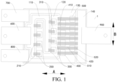
FIG. 1 is a schematic structural diagram of a semiconductor power module according to an embodiment of the present disclosure; -
FIG. 2 is a schematic structural diagram of a semiconductor power module according to another embodiment of the present disclosure; -
FIG. 3 is a schematic structural diagram of a semiconductor power module according to still another embodiment of the present disclosure; -
FIG. 4 is a schematic diagram of a connection of a substrate, a first DC transmission terminal, a second DC transmission terminal, a third DC transmission terminal, and an AC transmission terminal according to an embodiment of the present disclosure; -
FIG. 5 is a schematic diagram of a connection of a substrate, a first DC transmission terminal, a second DC transmission terminal, a third DC transmission terminal, and an AC transmission terminal from another perspective according to an embodiment of the present disclosure; -
FIG. 6 is a schematic diagram of a circuit of a semiconductor power module according to an embodiment of the present disclosure; -
FIG. 7 is a schematic diagram of a connection of a substrate, a third DC transmission terminal, and an AC transmission terminal according to an embodiment of the present disclosure; -
FIG. 8 is a schematic structural diagram of a substrate according to an embodiment of the present disclosure; -
FIG. 9 is a partial sectional view of a motor controller according to an embodiment of the present disclosure; -
FIG. 10 is a partial schematic structural diagram of a motor controller according to an embodiment of the present disclosure; and -
FIG. 11 is a schematic block diagram of a vehicle according to an embodiment of the present disclosure. - In the drawings:
-
Semiconductor power module 1,motor controller 2, -
substrate 100,insulation layer 101,circuit layer 102,heat dissipation layer 103, heatdissipation bottom plate 104, - first
conductive region 110, firsttransverse section 111, secondtransverse section 112, firstvertical section 113, - second
conductive region 120, thirdtransverse section 121, fourthtransverse section 122, secondvertical section 123, - third
conductive region 130, thirdvertical section 131, fourthvertical section 132, fifthtransverse section 133, sixthtransverse section 134, - fourth
conductive region 140, -
first power chip 200,first connection member 210, -
second power chip 300,second connection member 310, -
third power chip 400,third connection member 410,fourth connection member 420, -
fourth power chip 500,fifth connection member 510,sixth connection member 520, - first
DC transmission terminal 600, low-voltage connection part 610, - second
DC transmission terminal 700, first high-voltage connection part 710, - third
DC transmission terminal 800, second high-voltage connection part 810, -
AC transmission terminal 900,vehicle 1000,motor 1001;insulation cover 1100,coolant channel 1200, where - a first direction is a direction indicated by an arrow A, and a second direction is a direction indicated by an arrow B.
- The embodiments described with reference to accompanying drawings are exemplary, and the embodiments of the present disclosure are described in detail below.
- In the descriptions of the present disclosure, it should be understood that orientation or position relationships indicated by the terms such as "center", "longitudinal", "transverse", "length", "width", "thickness", "on", "below", "front", "back", "left", "right", "vertical", "horizontal", "top", "bottom", "inside", "outside", "clockwise", "counterclockwise", "axial direction", "radial direction", and "circumferential direction" are based on orientation or position relationships shown in the accompanying drawings, and are used only for ease and brevity of illustration and description, rather than indicating or implying that the mentioned apparatus or component needs to have a particular orientation or needs to be constructed and operated in a particular orientation.
- In the descriptions of the disclosure, "a plurality of" means two or more.
- A
semiconductor power module 1 according to the embodiments of the disclosure is described below with reference to the accompanying drawings. - As shown in
FIG. 1 to FIG. 10 , thesemiconductor power module 1 according to the embodiments of the present disclosure includes asubstrate 100, at least onefirst power chip 200, and at least onesecond power chip 300. - The
substrate 100 includes a first direction and a second direction orthogonal to each other. Thesubstrate 100 includes a firstconductive region 110 and a secondconductive region 120 that are spaced apart on thesubstrate 100. The firstconductive region 110 includes a firsttransverse section 111 and a secondtransverse section 112, and the secondconductive region 120 includes a thirdtransverse section 121 and a fourthtransverse section 122. The firsttransverse section 111, the thirdtransverse section 121, the secondtransverse section 112, and the fourthtransverse section 122 are sequentially arranged in the first direction. The firstconductive region 110 and the secondconductive region 120 are configured to transmit DC signals. Thefirst power chip 200 is respectively connected to the firsttransverse section 111 and the thirdtransverse section 121, and thesecond power chip 300 is respectively connected to the secondtransverse section 112 and the fourthtransverse section 122. - In other words, if the first direction is a length direction of the
substrate 100, the second direction is a width direction of thesubstrate 100. Alternatively, if the first direction is the width direction of thesubstrate 100, the second direction is the length direction of thesubstrate 100. This may be set based on an actual situation, such as a shape of thesubstrate 100, and is not limited. - For example, the
semiconductor power module 1 may be a silicon carbide metal oxide semiconductor field effect transistor (SiC MOSFET), or may be a device that cooperates with an IGBT (Insulated Gate Bipolar Transistor, insulated gate bipolar transistor) and an FRD (Fast recovery diode, fast recovery diode). - During actual application, the
semiconductor power module 1 needs to be packaged, for example, in a plastic sealing manner, to be specific, a process in which a semi-finished product of thesemiconductor power module 1 is injected and molded through plastic sealing, in other words, all structures in thesemiconductor power module 1 are mounted in a frame and plastic sealed, to form a plastic-sealed body module. Alternatively, a potting sealing manner may be used, to be specific, a process in which a semi-finished product of thesemiconductor power module 1 is potted and molded by using an insulating material such as silica gel, in other words, all structures in thesemiconductor power module 1 are mounted in a frame, and the silica gel is filled into the frame, to form a potting-sealed module. - It should be noted that, the
semiconductor power module 1 is a half-bridge power module, and may be used in a half-bridge circuit or a three-phase full-bridge circuit. For the plastic sealing manner, one singlesemiconductor power module 1 forms one plastic-sealed body, to be specific, one half-bridge circuit forms one plastic-sealed body; for the potting sealing manner, either one singlesemiconductor power module 1 may form one potting-sealed body, in other words, one half-bridge circuit forms one potting-sealed body, or threesemiconductor power modules 1 may form one potting-sealed body, in other words, the three-phase full-bridge circuit formed by three half-bridge circuits forms one potting-sealed body. - According to the
semiconductor power module 1 in this embodiment of the present disclosure, the firstconductive region 110 and the secondconductive region 120 are arranged on thesubstrate 100, to avoid a short circuit problem caused by an overlap between the firstconductive region 110 and the secondconductive region 120. In addition, the firstconductive region 110 includes the firsttransverse section 111 and the secondtransverse section 112, the secondconductive region 120 includes the thirdtransverse section 121 and the fourthtransverse section 122, and the firstconductive region 110 and the secondconductive region 120 are configured to transmit DC signals. The firsttransverse section 111 and the secondtransverse section 112 may be connected in series, and the thirdtransverse section 121 and the fourthtransverse section 122 may be connected in series. - In addition, the first
transverse section 111, the thirdtransverse section 121, the secondtransverse section 112, and the fourthtransverse section 122 are sequentially arranged in the first direction, thefirst power chip 200 is respectively connected to the firsttransverse section 111 and the thirdtransverse section 121, and thesecond power chip 300 is respectively connected to the secondtransverse section 112 and the fourthtransverse section 122. - If the
first power chip 200 is mounted on the firsttransverse section 111, thesecond power chip 300 is mounted on the secondtransverse section 112; if thefirst power chip 200 is mounted on the thirdtransverse section 121, thesecond power chip 300 is mounted on the fourthtransverse section 122. In other words, thefirst power chip 200 and thesecond power chip 300 are both mounted on the firstconductive region 110 or the secondconductive region 120, so that thefirst power chip 200 and thesecond power chip 300 form a series connection. - Because the
first power chip 200 and thesecond power chip 300 are necessarily separated by one of the secondtransverse section 112 and the thirdtransverse section 121, a distance between thefirst power chip 200 and thesecond power chip 300 is larger, so that heat accumulation of thefirst power chip 200 and thesecond power chip 300 can be avoided, and a heat dissipation effect of thesemiconductor power module 1 can be improved. - For example, when the
first power chip 200 and thesecond power chip 300 are respectively arranged on the firsttransverse section 111 and the secondtransverse section 112 of the firstconductive region 110, while a connection area between thefirst power chip 200 and thesecond power chip 300 and the firstconductive region 110 is ensured, a size of the firsttransverse section 111 and a size of the secondtransverse section 112 in the second direction do not need to be set to be excessively large, so that a size of thesemiconductor power module 1 in the second direction can be reduced. - In the related art, only the first transverse section and the second transverse section that are sequentially arranged in the first direction are provided, both the first power chip and the second power chip need to be mounted on the first transverse section, both the first power chip and the second power chip are connected to the second transverse section, and the first power chip is at a greater distance from the second transverse section than the second power chip. Therefore, a connection structure between the second transverse section and the first power chip needs to be set to be long, and thus the connection structure between the second transverse section and the first power chip not only generates more heat, but also has a problem of a large stray inductance. However, in the
semiconductor power module 1 in this embodiment of the present disclosure, thefirst power chip 200 is connected to the thirdtransverse section 121, and thesecond power chip 300 is connected to the fourthtransverse section 122. Therefore, a size of a connection structure between the secondconductive region 120 and either of thefirst power chip 200 and thesecond power chip 300 is small, which not only generates less heat and facilitates heat dissipation, but also reduces a stray inductance and helps reduce a switching loss. - For example, when the
first power chip 200 and thesecond power chip 300 are respectively arranged on the thirdtransverse section 121 and the fourthtransverse section 122 of the secondconductive region 120, while a connection area between thefirst power chip 200 and thesecond power chip 300 and the secondconductive region 120 is ensured, a size of the thirdtransverse section 121 and a size of the fourthtransverse section 122 in the second direction do not need to be set to be excessively large, so that a size of thesemiconductor power module 1 in the second direction may be reduced. - In addition, in the related art, the first conductive region is provided with only the first transverse section, that is, the first conductive region is not provided with the second transverse section, and both the first power chip and the second power chip need to be connected to the first transverse section. Therefore, a connection structure between the first transverse section and the second power chip needs to be set to be long, and thus the connection structure between the first transverse section and the second power chip not only generates more heat, but also has a problem of a large stray inductance. However, in the
semiconductor power module 1 in this embodiment of the present disclosure, thefirst power chip 200 is connected to the firsttransverse section 111, and thesecond power chip 300 is connected to the secondtransverse section 112. Therefore, a size of a connection structure between the firstconductive region 110 and either of thefirst power chip 200 and thesecond power chip 300 is small, which not only generates less heat and facilitates heat dissipation, but also reduces a stray inductance and helps reduce a switching loss. - In summary, it can be learned that the
semiconductor power module 1 in this embodiment of the present disclosure has a small stray inductance, a low temperature at a position of the power chip, and a very good heat dissipation effect, which is conducive to applying thesemiconductor power module 1 to a circuit with a high switching speed. - In this way, the
semiconductor power module 1 according to this embodiment of the present disclosure has advantages such as the small stray inductance and the good heat dissipation effect. - According to some specific embodiments of the present disclosure, in
FIG. 4 andFIG. 5 , the firstconductive region 110 further includes a firstvertical section 113. The firsttransverse section 111 and the secondtransverse section 112 both extend in the second direction, the firstvertical section 113 extends in the first direction, and two ends of the firstvertical section 113 are respectively connected to the firsttransverse section 111 and the secondtransverse section 112. The secondconductive region 120 further includes a secondvertical section 123. The thirdtransverse section 121 and the fourthtransverse section 122 both extend in the second direction, the secondvertical section 123 extends in the first direction, and two ends of the secondvertical section 123 are respectively connected to the thirdtransverse section 121 and the fourthtransverse section 122. The firstvertical section 113 and the secondvertical section 123 are respectively arranged adjacent to two opposite sides of thesubstrate 100 in the second direction. - In other words, the first
conductive region 110 forms a "U"-shaped structure, and the secondconductive region 120 forms a "U"-shaped structure. The firstconductive region 110 is inserted into the secondconductive region 120 from an opening of the secondconductive region 120, and the secondconductive region 120 is inserted into the firstconductive region 110 from an opening of the firstconductive region 110. - In this way, the first
transverse section 111 and the secondtransverse section 112 are connected in series through the firstvertical section 113, and the thirdtransverse section 121 and the fourthtransverse section 122 are connected in series through the secondvertical section 123, so that thefirst power chip 200 and thesecond power chip 300 can be connected in series, and the firstconductive region 110 and the secondconductive region 120 occupy less space as a whole. - According to some specific embodiments of the present disclosure, in
FIG. 4 andFIG. 5 , one end of the firstvertical section 113 is flush with a side of the firsttransverse section 111 that faces away from the secondtransverse section 112, and the other end of the firstvertical section 113 is flush with a side of the secondtransverse section 112 that faces away from the firsttransverse section 111; one end of the secondvertical section 123 is flush with a side of the thirdtransverse section 121 that faces away from the fourthtransverse section 122, and the other end of the secondvertical section 123 is flush with a side of the fourthtransverse section 122 that faces away from the thirdtransverse section 121. - In other words, a sum of sizes of the first
vertical section 113 and the fourthtransverse section 122 in the first direction is equal to a sum of sizes of the secondvertical section 123 and the firsttransverse section 111 in the first direction. In this way, the firstconductive region 110 and the secondconductive region 120 occupy less space as a whole in the first direction, and thefirst power chip 200 and thesecond power chip 300 are distributed more evenly in the first direction. - According to some specific embodiments of the present disclosure, in
FIG. 4 andFIG. 5 , a side of the firstvertical section 113 that faces away from the secondvertical section 123 is flush with an end of the fourthtransverse section 122 away from the secondvertical section 123, and a side of the secondvertical section 123 that faces away from the firstvertical section 113 is flush with a side of the firsttransverse section 111 away from the firstvertical section 113. - In other words, a length of the first
transverse section 111 may be the same as a length of the fourthtransverse section 122, a length of the secondtransverse section 112 may be the same as a length of the thirdtransverse section 121, a sum of sizes of the secondtransverse section 112 and the secondvertical section 123 in the second direction is substantially equal to the length of the firsttransverse section 111, and a sum of sizes of the thirdtransverse section 121 and the firstvertical section 113 in the second direction is substantially equal to the length of the fourthtransverse section 122. - In this way, the first
conductive region 110 and the secondconductive region 120 occupy less space as a whole in the second direction, thus helping to reduce a volume of thesemiconductor power module 1. - According to some specific embodiments of the present disclosure, in
FIG. 1 to FIG. 3 , thefirst power chip 200 is mounted on the thirdtransverse section 121, thefirst power chip 200 is connected to the firsttransverse section 111 through afirst connection member 210, and thefirst connection member 210 is perpendicular to the firsttransverse section 111 and the thirdtransverse section 121. Thefirst connection member 210 may be an aluminum wire, a copper wire, a gold wire, a copper strip, an aluminum strip, a copper connecting piece, or the like, and thefourth connection member 420 may be an aluminum wire, a copper wire, a gold wire, a copper strip, an aluminum strip, a copper connecting piece, or the like. - In this way, the
first connection member 210 and thefirst power chip 200 can implement a connection between the firstconductive region 110 and the secondconductive region 120. In addition, a length of thefirst connection member 210 is short, so that a parasitic inductance generated by thefirst connection member 210 in a circuit can be reduced, thereby reducing a switching loss, and an internal layout is more proper. - According to some specific embodiments of the present disclosure, in
FIG. 1 to FIG. 3 , thesecond power chip 300 is mounted on the fourthtransverse section 122, thesecond power chip 300 is connected to the secondtransverse section 112 through thesecond connection member 310, and thesecond connection member 310 is perpendicular to the secondtransverse section 112 and the fourthtransverse section 122. Thesecond connection member 310 may be an aluminum wire, a copper wire, a gold wire, a copper strip, an aluminum strip, a copper connecting piece, or the like, and thefourth connection member 420 may be an aluminum wire, a copper wire, a gold wire, a copper strip, an aluminum strip, a copper connecting piece, or the like. - In this way, the
second connection member 310 and thesecond power chip 300 can implement a connection between the firstconductive region 110 and the secondconductive region 120. In addition, a length of thesecond connection member 310 is short, so that a parasitic inductance generated by thesecond connection member 310 in a circuit can be reduced, thereby reducing a switching loss, and an internal layout is more proper. In addition, thefirst power chip 200 and thesecond power chip 300 are more dispersed, so that heat accumulation may be reduced, thereby improving a heat dissipation capability of thesemiconductor power module 1. - According to some specific embodiments of the present disclosure, in
FIG. 1 to FIG. 5 , thesemiconductor power module 1 further includes a thirdconductive region 130, athird power chip 400, and afourth power chip 500. - The third
conductive region 130 is arranged on thesubstrate 100 and is spaced apart from the firstconductive region 110 and the secondconductive region 120, and the thirdconductive region 130 is constructed in a closed loop shape arranged around the firstconductive region 110 and the secondconductive region 120. - Specifically, the third
conductive region 130 includes a thirdvertical section 131, a fourthvertical section 132, a fifthtransverse section 133, and a sixthtransverse section 134; the thirdvertical section 131 and the fourthvertical section 132 extend in the first direction and are spaced apart in the second direction, the fifthtransverse section 133 and the sixthtransverse section 134 extend in the second direction and are spaced apart in the first direction; the thirdvertical section 131, the fifthtransverse section 133, the fourthvertical section 132, and the sixthtransverse section 134 are sequentially connected end to end; the firstconductive region 110 and the secondconductive region 120 are located between the thirdvertical section 131 and the fourthvertical section 132 in the second direction; the fifthtransverse section 133 is located on a side of the fourthtransverse section 122 that faces away from the thirdtransverse section 121 in the first direction, and the thirdconductive region 130 is configured to transmit the DC signals, thethird power chip 400 and thefourth power chip 500 are arranged on the fifthtransverse section 133 and are both connected to the fourthtransverse section 122. - In other words, the
first power chip 200, thesecond power chip 300, thethird power chip 400, and thefourth power chip 500 are respectively arranged in the firstconductive region 110, the secondconductive region 120, and the thirdconductive region 130, thereby avoiding a problem of heat increase caused by a compact power chip layout, and improving the heat dissipation capacity of thesemiconductor power module 1. - In addition, the
third power chip 400 and thefourth power chip 500 form a series connection on the thirdconductive region 130. Through this arrangement, inductances formed inside thesemiconductor power module 1 may cancel each other when thesemiconductor power module 1 works, so as to effectively reduce a parasitic inductance of the entire module, and optimize a structural layout inside thesemiconductor power module 1, thereby improving integration of thesemiconductor power module 1. - In addition, both the
third power chip 400 and thefourth power chip 500 are connected to the secondconductive region 120, so that the firstconductive region 110, the secondconductive region 120, and the thirdconductive region 130 are electrically connected to each other, and thesemiconductor power module 1 can implement DC input/output. - According to some specific embodiments of the present disclosure, in
FIG. 1 to FIG. 5 , multiplethird power chips 400 are spaced apart in the second direction, and the multiplethird power chips 400 are arranged in a row in the second direction. Multiplefourth power chips 500 are spaced apart in the second direction, and the multiplefourth power chips 500 are arranged in a row in the second direction. The row in which thethird power chip 400 is located and the row in which thefourth power chip 500 is located are spaced apart in the first direction. A sum of the quantities of thefirst power chips 200 and thesecond power chips 300 is the same as a sum of the quantities of thethird power chips 400 and thefourth power chips 500. - For example, the
third power chips 400 may be in a one-to-one correspondence with thefirst power chips 200, and thefourth power chips 500 may be in a one-to-one correspondence with thesecond power chips 300. In addition, a sum of the quantities of thefirst power chips 200 and thesecond power chips 300 may be set based on an output current of thesemiconductor power module 1. For example, the sum of the quantities of thefirst power chips 200 and thesecond power chips 300 may be 6, 7, or 8. Certainly, the sum of the quantities of thefirst power chips 200 and thesecond power chips 300 may alternatively be another quantity, provided that usage requirements of different scenarios of thesemiconductor power module 1 are met. - According to some specific embodiments of the present disclosure, in
FIG. 1 to FIG. 3 , the multiplethird power chips 400 and the multiplefourth power chips 500 are arranged alternately in the second direction. In this way, wiring between thethird power chip 400 and thefourth power chip 500 is less prone to interference, and an electrical connection is safer, so that space utilization of thesemiconductor power module 1 is improved, and thethird power chip 400 and thefourth power chip 500 are arranged more dispersedly, thereby further improving heat dissipation performance of thesemiconductor power module 1. - According to some specific embodiments of the present disclosure, in
FIG. 1 to FIG. 5 , thesemiconductor power module 1 further includes a fourthconductive region 140. The fourthconductive region 140 is arranged on thesubstrate 100 and is respectively spaced apart from the firstconductive region 110, the secondconductive region 120, and the thirdconductive region 130. The fourthconductive region 140 extends in the second direction and is located on a side of the fifthtransverse section 133 that faces away from the fourthtransverse section 122 in the first direction. Both thethird power chip 400 and thefourth power chip 500 are connected to the fourthconductive region 140, and the fourthconductive region 140 is configured to transmit the AC signals. - In this way, the
semiconductor power module 1 can implement a function of circuit conversion between a direct current and an alternating current, and thesemiconductor power module 1 may be a half-bridge circuit. - According to some specific embodiments of the present disclosure, in
FIG. 1 to FIG. 3 , thethird power chip 400 is connected to the fourthtransverse section 122 through thethird connection member 410, and thethird connection member 410 is perpendicular to the fourthtransverse section 122 and the fifthtransverse section 133. Thethird power chip 400 is connected to the fourthconductive region 140 by thefourth connection member 420, and thefourth connection member 420 is perpendicular to the fifthtransverse section 133 and the fourthconductive region 140. Thethird connection member 410 may be an aluminum wire, a copper wire, a gold wire, a copper strip, an aluminum strip, a copper connecting piece, or the like, and thefourth connection member 420 may be an aluminum wire, a copper wire, a gold wire, a copper strip, an aluminum strip, a copper connecting piece, or the like. - In other words, the
third connection member 410 and thefourth connection member 420 are parallel, the fourthtransverse section 122, the fifthtransverse section 133, and the fourthconductive region 140 are parallel, and thethird connection member 410 and thefourth connection member 420 are respectively perpendicular to the fourthtransverse section 122, the fifthtransverse section 133, and the fourthconductive region 140. - In this way, lengths of the
third connection member 410 and thefourth connection member 420 are smaller, so that a line arrangement can be simplified, and inductances generated by thethird connection member 410 and thefourth connection member 420 can be reduced, thereby reducing a switching loss and heat generation, and improving heat dissipation performance. - According to some specific embodiments of the present disclosure, in
FIG. 1 to FIG. 3 , thethird connection member 410 and thefourth connection member 420 are configured as an integrated member extending in the first direction. In this way, arrangement difficulty can be reduced, production efficiency can be improved, less inductance is generated, and functional performance of thesemiconductor power module 1 is better. - According to some specific embodiments of the present disclosure, in
FIG. 1 to FIG. 3 , thefourth connection member 420 and thefourth power chip 500 are spaced apart in the second direction. In this way, contact between thefourth connection member 420 and thefourth power chip 500 can be avoided, thus reliability of the electrical connection can be prevented from being affected, thereby ensuring effectiveness of thesemiconductor power module 1. - According to some specific embodiments of the present disclosure, in
FIG. 1 to FIG. 3 , thefourth power chip 500 is connected to the fourthtransverse section 122 through thefifth connection member 510, and thefifth connection member 510 is perpendicular to the fourthtransverse section 122 and the fifthtransverse section 133. Thefourth power chip 500 is connected to the fourthconductive region 140 through thesixth connection member 520, and thesixth connection member 520 is perpendicular to the fifthtransverse section 133 and the fourthconductive region 140. Thefifth connection member 510 may be an aluminum wire, a copper wire, a gold wire, a copper strip, an aluminum strip, a copper connecting piece, or the like, and thesixth connection member 520 may be an aluminum wire, a copper wire, a gold wire, a copper strip, an aluminum strip, a copper connecting piece, or the like. - In other words, the
fifth connection member 510 and thesixth connection member 520 are parallel, the fourthtransverse section 122, the fifthtransverse section 133, and the fourthconductive region 140 are parallel, and thefifth connection member 510 and thesixth connection member 520 are respectively perpendicular to the fourthtransverse section 122, the fifthtransverse section 133, and the fourthconductive region 140. - In this way, lengths of the
fifth connection member 510 and thesixth connection member 520 are smaller, so that a line arrangement can be simplified, and inductances generated by thefifth connection member 510 and thesixth connection member 520 can be reduced, thereby reducing a switching loss and heat generation, and improving heat dissipation performance. - According to some specific embodiments of the present disclosure, in
FIG. 1 to FIG. 3 , thefifth connection member 510 and thesixth connection member 520 are configured as an integrated member extending in the first direction. In this way, arrangement difficulty can be reduced, production efficiency can be improved, less inductance is generated, and functional performance of thesemiconductor power module 1 is better. - According to some specific embodiments of the present disclosure, in
FIG. 1 to FIG. 3 , thefifth connection member 510 and thethird power chip 400 are spaced apart in the second direction. In this way, contact between thefifth connection member 510 and thethird power chip 400 can be avoided, thus reliability of the electrical connection can be prevented from being affected, thereby ensuring effectiveness of thesemiconductor power module 1. - According to some specific embodiments of the present disclosure, in
FIG. 4 to FIG. 7 , thesemiconductor power module 1 further includes a firstDC transmission terminal 600, a secondDC transmission terminal 700, a thirdDC transmission terminal 800, and aAC transmission terminal 900. - The first
DC transmission terminal 600 is connected to the firsttransverse section 111 and extends beyond the edge of thesubstrate 100, the secondDC transmission terminal 700 is connected to an end of the thirdvertical section 131 away from the fifthtransverse section 133 and extends beyond the edge of thesubstrate 100, the thirdDC transmission terminal 800 is connected to an end of the fourthvertical section 132 away from the fifthtransverse section 133 and extends beyond the edge of thesubstrate 100, and theAC transmission terminal 900 is connected to the fourthconductive region 140 and extends beyond the edge of thesubstrate 100. - For example, the first
DC transmission terminal 600, the secondDC transmission terminal 700, and the thirdDC transmission terminal 800 are located on one of two opposite sides of thesubstrate 100, and theAC transmission terminal 900 is located on the other of the two opposite sides of thesubstrate 100. In this way, a connection between the alternating current and the direct current does not interfere with each other, and electrical connection safety is improved. In addition, a conductive circuit between the secondDC transmission terminal 700 and theAC transmission terminal 900 may form a first bridge arm, and a conductive circuit between the thirdDC transmission terminal 800 and theAC transmission terminal 900 may form a second bridge arm. Inductances formed between a circuit formed by the first bridge arm and a circuit formed by the second bridge arm cancel each other out, thereby reducing a parasitic inductance of the entiresemiconductor power module 1, improving a filtering capability of thesemiconductor power module 1, and reducing a switching loss. - In
FIG. 6 , dashed arrows show a current flow direction in an optional working state of thesemiconductor power module 1. It may be understood that, thesemiconductor power module 1 may alternatively have another current flow direction in the working state, for example, a current flow direction on each conductive region itself. Certainly, thesemiconductor power module 1 may alternatively have a current flow direction of another manner in another working state. - According to some specific embodiments of the present disclosure, in
FIG. 5 , the first high-voltage connection part 710 is arranged at an end of the thirdvertical section 131 away from the fifthtransverse section 133. A size of the first high-voltage connection part 710 in the second direction is greater than a width of the thirdvertical section 131 and greater than a width of the secondDC transmission terminal 700. The secondDC transmission terminal 700 is connected to the first high-voltage connection part 710. A width of the thirdvertical section 131 is less than a width of the secondDC transmission terminal 700, so that a size of thesemiconductor power module 1 in the second direction is reduced, thereby facilitating miniaturization of thesemiconductor power module 1. - By arranging the first high-
voltage connection part 710, the thirdvertical section 131 can be connected to the secondDC transmission terminal 700, and in addition, the secondDC transmission terminal 700 does not extend beyond the first high-voltage connection part 710 in the second direction, so that a contact area between the secondDC transmission terminal 700 and the thirdvertical section 131 is improved, thereby ensuring reliability of an electrical connection between the secondDC transmission terminal 700 and the thirdvertical section 131. - In addition, the second high-
voltage connection part 810 is arranged at an end of the fourthvertical section 132 away from the fifthtransverse section 133. A size of the second high-voltage connection part 810 in the second direction is greater than a width of the fourthvertical section 132 and greater than a width of the thirdDC transmission terminal 800, and the thirdDC transmission terminal 800 is connected to the second high-voltage connection part 810. A width of the fourthvertical section 132 is less than a width of the thirdDC transmission terminal 800, so that a size of thesemiconductor power module 1 in the second direction is reduced, thereby facilitating miniaturization of thesemiconductor power module 1. - By arranging the second high-
voltage connection part 810, the fourthvertical section 132 can be connected to the thirdDC transmission terminal 800, and in addition, the thirdDC transmission terminal 800 does not extend beyond the second high-voltage connection part 810 in the second direction, so that a contact area between the thirdDC transmission terminal 800 and the fourthvertical section 132 is improved, thereby ensuring reliability of an electrical connection between the thirdDC transmission terminal 800 and the fourthvertical section 132. - According to some embodiments of the present disclosure, in
FIG. 5 , a low-voltage connection part 610 is arranged on a side of the firsttransverse section 111 that faces away from the secondtransverse section 112. A length of the low-voltage connection part 610 is less than a length of the firsttransverse section 111 and greater than a width of the firstDC transmission terminal 600. The firstDC transmission terminal 600 is connected to the low-voltage connection part 610. - The first high-
voltage connection part 710 and the second high-voltage connection part 810 are located on two opposite sides of the low-voltage connection part 610 in the second direction. Through making the length of the low-voltage connection part 610 less than the length of the firsttransverse section 111, the low-voltage connection part 610 can avoid the first high-voltage connection part 710 and the second high-voltage connection part 810. In addition, while a reliable connection between the low-voltage connection part 610 and the low-voltage connection part 610 is ensured, a size of thesemiconductor power module 1 in the second direction is prevented from increasing, thereby facilitating miniaturization of thesemiconductor power module 1. - By arranging the low-
voltage connection part 610, the firsttransverse section 111 can be connected to the low-voltage connection part 610, and in addition, the low-voltage connection part 610 does not extend beyond the firsttransverse section 111 in the second direction, thereby ensuring reliability of an electrical connection between the firstDC transmission terminal 600 and the firsttransverse section 111. - According to some specific embodiments of this the present disclosure, in
FIG. 5 , a width of the secondDC transmission terminal 700 is the same as a width of the thirdDC transmission terminal 800 and is less than a width of the firstDC transmission terminal 600. Because the secondDC transmission terminal 700 and the thirdDC transmission terminal 800 are both connected to the thirdconductive region 130, the width of the firstDC transmission terminal 600 may be substantially equal to a sum of the width of the secondDC transmission terminal 700 and the width of the thirdDC transmission terminal 800, to ensure that a direct current input impedance is substantially the same as a direct current output impedance, thereby reducing heat generation of thesemiconductor power module 1. - According to some specific embodiments of the present disclosure, in
FIG. 7 and FIG. 8 , thesubstrate 100 includes aninsulation layer 101, acircuit layer 102, and aheat dissipation layer 103. Thecircuit layer 102 is connected to a side of theinsulation layer 101 in a thickness direction, the firstconductive region 110 and the secondconductive region 120 are formed on thecircuit layer 102, and theheat dissipation layer 103 is connected to the other side of theinsulation layer 101 in the thickness direction. - The
insulation layer 101 may be made of ceramic, for example, made of aluminum oxide (Al2O3), aluminum nitride (AlN), and silicon nitride (Si3N4). In this way, theinsulation layer 101 has a good heat conduction effect, a strong insulation capability, and a stable chemical property, which may not only isolate a connection between the conductive layer and theheat dissipation layer 103, but also provide a heat dissipation channel for thesemiconductor power module 1. - The
circuit layer 102 may be made of a copper material, and the copper is etched into the firstconductive region 110, the secondconductive region 120, the thirdconductive region 130, and the fourthconductive region 140. Theheat dissipation layer 103 may be made of a copper material, and the firstDC transmission terminal 600, the secondDC transmission terminal 700, the thirdDC transmission terminal 800, and theAC transmission terminal 900 may all be made of copper materials. In this way, thecircuit layer 102, theheat dissipation layer 103, the firstDC transmission terminal 600, the secondDC transmission terminal 700, the thirdDC transmission terminal 800, and theAC transmission terminal 900 all have good conductivity performance and heat dissipation performance, and can be effectively connected to an external device. - According to some specific embodiments of the present disclosure, in
FIG. 1 ,FIG. 2 ,FIG. 3 , andFIG. 9 , thesemiconductor power module 1 further includes aninsulation cover 1100. Theinsulation cover 1100 is mounted on thesubstrate 100 and covers the firstconductive region 110, the secondconductive region 120, thefirst power chip 200, and thesecond power chip 300. Theinsulation cover 1100 may insulate and protect a device, thereby improving safety of an electrical connection of thesemiconductor power module 1. - A
motor controller 2 according to an embodiment of the present disclosure is described below with reference to the accompanying drawings. InFIG. 9 and FIG. 10 , themotor controller 2 includes a heatdissipation bottom plate 104, acoolant channel 1200, and thesemiconductor power module 1 according to the foregoing embodiments of the present disclosure. The heatdissipation bottom plate 104 is mounted in thecoolant channel 1200, and thesemiconductor power module 1 is arranged on the heatdissipation bottom plate 104. - For example, there are multiple
semiconductor power modules 1 and are arranged on the heatdissipation bottom plate 104 in the second direction, and the multiplesemiconductor power modules 1 may be arranged in parallel. A bottom of eachsemiconductor power module 1 is welded to the heatdissipation bottom plate 104. Thecoolant channel 1200 may be an open-groove water channel, and the heatdissipation bottom plate 104 is mounted on the open groove of thecoolant channel 1200, so that a heat dissipation function for thesemiconductor power module 1 is implemented. This design process is simple, easy to implement, and convenient to operate. - In this embodiment, the
semiconductor power module 1 provided based on the foregoing embodiments has a uniform structural layout and a good heat dissipation effect, and themotor controller 2 can be used in various coolant channel applications, such as a series coolant channel or a parallel coolant channel, so that application flexibility of themotor controller 2 is improved, and a stray inductance in a loop during application is reduced. - By using the
semiconductor power module 1 according to the foregoing embodiment of the present disclosure, themotor controller 2 according to the embodiment of the present disclosure has advantages such as a small stray inductance and a good heat dissipation effect. - A
vehicle 1000 according to an embodiment of the present disclosure is described below with reference toFIG. 11 . Thevehicle 1000 includes amotor 1001 and themotor controller 2 according to the foregoing embodiment of the present disclosure. Themotor controller 2 is connected to themotor 1001. - By using the
motor controller 2 according to the embodiment of the present disclosure, the vehicle according to the embodiment of the present disclosure has advantages such as a small stray inductance and a good heat dissipation effect. - Other configurations and operations of the
semiconductor power module 1, themotor controller 2, and the vehicle according to the embodiments of the present disclosure are known to a person of ordinary skill in the art and will not be described in detail herein. - In the description of this specification, the description of the reference terms such as "an embodiment", "some embodiments", "exemplary embodiments", "example", "specific example", or "some examples" means that the specific features, structures, materials or characteristics described with reference to the embodiment or example are included in at least one embodiment or example of the present disclosure. In this specification, schematic descriptions of the foregoing terms are not necessarily directed at a same embodiment or example.
- Although the embodiments of the present disclosure have been shown and described, a person of ordinary skill in the art should understand that various changes, modifications, replacements and variations may be made to the embodiments without departing from the principles and spirit of the present disclosure, and the scope of the present disclosure is as defined by the appended claims and their equivalents.
Claims (25)
- A semiconductor power module (1), comprising:a substrate (100), the substrate (100) comprising a first direction and a second direction orthogonal to each other;a first conductive region (110), the first conductive region (110) comprising a first transverse section (111) and a second transverse section (112);a second conductive region (120), the second conductive region (120) and the first conductive region (110) being spaced apart on the substrate (100); the second conductive region (120) comprising a third transverse section (121) and a fourth transverse section (122); and the first transverse section (111), the third transverse section (121), the second transverse section (112), and the fourth transverse section (122) being sequentially arranged in the first direction, wherein the first conductive region (110) and the second conductive region (120) are configured to transmit DC signals;at least one first power chip (200), the first power chip (200) being respectively connected to the first transverse section (111) and the third transverse section (121); andat least one second power chip (300), the second power chip (300) being respectively connected to the second transverse section (112) and the fourth transverse section (122).
- The semiconductor power module (1) according to claim 1, wherein the first conductive region (110) further comprises a first vertical section (113), the first transverse section (111) and the second transverse section (112) both extend in the second direction, the first vertical section (113) extends in the first direction, and two ends of the first vertical section (113) are respectively connected to the first transverse section (111) and the second transverse section (112);the second conductive region (120) further comprises a second vertical section (123), the third transverse section (121) and the fourth transverse section (122) both extend in the second direction, the second vertical section (123) extends in the first direction, and two ends of the second vertical section (123) are respectively connected to the third transverse section (121) and the fourth transverse section (122); andthe first vertical section (113) and the second vertical section (123) are respectively arranged adjacent to two opposite sides of the substrate (100) in the second direction.
- The semiconductor power module (1) according to claim 2, wherein an end of the first vertical section (113) is flush with a side of the first transverse section (111) that faces away from the second transverse section (112), and another end of the first vertical section (113) is flush with a side of the second transverse section (112) that faces away from the first transverse section (111); and
an end of the second vertical section (123) is flush with a side of the third transverse section (121) that faces away from the fourth transverse section (122), and another end of the second vertical section (123) is flush with a side of the fourth transverse section (122) that faces away from the third transverse section (121). - The semiconductor power module (1) according to claim 2 or 3, wherein a side of the first vertical section (113) that faces away from the second vertical section (123) is flush with an end of the fourth transverse section (122) away from the second vertical section (123); and
a side of the second vertical section (123) that faces away from the first vertical section (113) is flush with a side of the first transverse section (111) away from the first vertical section (113). - The semiconductor power module (1) according to any one of claims 1 to 4, wherein the first power chip (200) is mounted on the third transverse section (121), and the first power chip (200) is connected to the first transverse section (111) through a first connection member (210).
- The semiconductor power module (1) according to any one of claims 1 to 5, wherein the second power chip (300) is mounted on the fourth transverse section (122), and the second power chip (300) is connected to the second transverse section (112) through a second connection member (310).
- The semiconductor power module (1) according to any one of claims 1 to 6, further comprising:
a third conductive region (130), the third conductive region (130) being arranged on the substrate (100) and spaced apart from the first conductive region (110) and the second conductive region (120), and the third conductive region (130) being constructed in a closed loop shape arranged around the first conductive region (110) and the second conductive region (120). - The semiconductor power module (1) according to claim 7, wherein
the third conductive region (130) comprises:a third vertical section (131);a fourth vertical section (132), the fourth vertical section (132) and the third vertical section (131) extending in the first direction and being spaced apart from each other in the second direction;a fifth transverse section (133); anda sixth transverse section (134), the sixth transverse section (134) and the fifth transverse section (133) extending in the second direction and being spaced apart in the first direction; the third vertical section (131), the fifth transverse section (133), the fourth vertical section (132), and the sixth transverse section (134) being sequentially connected end to end; the first conductive region (110) and the second conductive region (120) being located between the third vertical section (131) and the fourth vertical section (132) in the second direction; and the fifth transverse section (133) being located on the side of the fourth transverse section (122) that faces away from the third transverse section (121) in the first direction, wherein the third conductive region (130) is configured to transmit DC signals; andthe semiconductor power module further comprises:at least one third power chip (400), the third power chip (400) being arranged on the fifth transverse section (133), and the third power chip (400) being connected to the fourth transverse section (122); andat least one fourth power chip (500), the fourth power chip (500) being arranged on the fifth transverse section (133), and the fourth power chip (500) being connected to the fourth transverse section (122). - The semiconductor power module (1) according to claim 8, wherein a plurality of third power chips (400) are comprised, the plurality of third power chips (400) are spaced apart in the second direction, and the plurality of third power chips (400) are arranged in a row in the second direction; anda plurality of fourth power chips (500) are comprised, the plurality of fourth power chips (500) are spaced apart in the second direction, and the plurality of fourth power chips (500) are arranged in a row in the second direction;the row in which the third power chips (400) are located and the row in which the fourth power chips (500) are located are spaced apart in the first direction; anda sum of a quantity of first power chips (200) and a quantity of second power chips (300) is the same as a sum of a quantity of the third power chips (400) and a quantity of the fourth power chips (500).
- The semiconductor power module (1) according to claim 9, wherein the plurality of third power chips (400) and the plurality of fourth power chips (500) are alternately arranged in the second direction.
- The semiconductor power module (1) according to any one of claims 8 to 10, comprising:a fourth conductive region (140), the fourth conductive region (140) being arranged on the substrate (100) and spaced apart from the first conductive region (110), the second conductive region (120), and the third conductive region (130); the fourth conductive region (140) extending in the second direction and being located on a side of the fifth transverse section (133) that faces away from the fourth transverse section (122) in the first direction, and the third power chip (400) and the fourth power chip (500) being both connected to the fourth conductive region (140),wherein the fourth conductive region (140) is configured to transmit AC signals.
- The semiconductor power module (1) according to claim 11, wherein the third power chip (400) is connected to the fourth transverse section (122) through a third connection member (410); and
the third power chip (400) is connected to the fourth conductive region (140) through a fourth connection member (420). - The semiconductor power module (1) according to claim 12, wherein the third connection member (410) and the fourth connection member (420) are constructed as an integrated member extending in the first direction.
- The semiconductor power module (1) according to claim 12 or 13, wherein the fourth connection member (420) and the fourth power chip (500) are spaced apart in the second direction.
- The semiconductor power module (1) according to any one of claims 11 to 14, wherein the fourth power chip (500) is connected to the fourth transverse section through a fifth connection member (510); and
the fourth power chip (500) is connected to the fourth conductive region (140) through a sixth connection member (520). - The semiconductor power module (1) according to claim 15, wherein the fifth connection member (510) and the sixth connection member (520) are constructed as an integrated member extending in the first direction.
- The semiconductor power module (1) according to claim 15 or 16, wherein the fifth connection member (510) and the third power chip (400) are spaced apart in the second direction.
- The semiconductor power module (1) according to any one of claims 11 to 17, comprising:a first DC transmission terminal (600), the first DC transmission terminal (600) being connected to the first transverse section (111) and extending beyond an edge of the substrate (100);a second DC transmission terminal (700), the second DC transmission terminal (700) being connected to an end of the third vertical section (131) away from the fifth transverse section (133) and extending beyond the edge of the substrate (100);a third DC transmission terminal (800), the third DC transmission terminal (800) being connected to an end of the fourth vertical section (132) away from the fifth transverse section (133) and extending beyond the edge of the substrate (100); andan AC transmission terminal (900), the AC transmission terminal (900) being connected to the fourth conductive region (140) and extending beyond the edge of the substrate (100).
- The semiconductor power module (1) according to claim 18, further comprising:
a low-voltage connection part (610), the low-voltage connection part (610) being arranged on the side of the first transverse section (111) that faces away from the second transverse section (112), a length of the low-voltage connection part (610) being less than a length of the first transverse section (111) and greater than a width of the first DC transmission terminal (600), and the first DC transmission terminal (600) being connected to the low-voltage connection part (610). - The semiconductor power module (1) according to claim 18 or 19, further comprising:a first high-voltage connection part (710), the first high-voltage connection part (710) being arranged on the end of the third vertical section (131) away from the fifth transverse section (133), a size of the first high-voltage connection part (710) in the second direction being greater than a width of the third vertical section (131) and greater than a width of the second DC transmission terminal (700), and the second DC transmission terminal (700) being connected to the first high-voltage connection part (710); anda second high-voltage connection part (810), the second high-voltage connection part (810) being arranged on the end of the fourth vertical section (132) away from the fifth transverse section (133), a size of the second high-voltage connection part (810) in the second direction being greater than a width of the fourth vertical section (132) and greater than a width of the third DC transmission terminal (800), and the third DC transmission terminal (800) being connected to the second high-voltage connection part (810).
- The semiconductor power module (1) according to any one of claims 1 to 20, wherein the substrate (100) comprises:an insulation layer (101);a circuit layer (102), the circuit layer (102) being connected to a side of the insulation layer (101) in a thickness direction, and the first conductive region (110) and the second conductive region (120) being formed on the circuit layer (102); anda heat dissipation layer (103), the heat dissipation layer (103) being connected to another side of the insulation layer (101) in the thickness direction.
- The semiconductor power module (1) according to any one of claims 1 to 21, further comprising:
an insulation cover (1100), the insulation cover (1100) being mounted on the substrate (100) and covering the first conductive region (110), the second conductive region (120), the first power chip (200), and the second power chip (300). - A motor controller (2), comprising:a heat dissipation bottom plate (104);a coolant channel (1200), the heat dissipation bottom plate (104) being mounted in the coolant channel (1200); andthe semiconductor power module (1) according to any one of claims 1 to 22, the semiconductor power module (1) being arranged on the heat dissipation bottom plate (104).
- The motor controller (2) according to claim 23, wherein a plurality of semiconductor power modules (1) are arranged on the heat dissipation bottom plate (104) in the second direction.
- A vehicle (1000), comprising:a motor (1001); andthe motor controller (2) according to claim 23 or 24, the motor controller (2) being connected to the motor (1001).
Applications Claiming Priority (2)
| Application Number | Priority Date | Filing Date | Title |
|---|---|---|---|
| CN202211058483.1A CN117690897A (en) | 2022-08-31 | 2022-08-31 | Semiconductor power modules, motor controllers and vehicles |
| PCT/CN2023/110386 WO2024045990A1 (en) | 2022-08-31 | 2023-07-31 | Semiconductor power module, motor controller, and vehicle |
Publications (2)
| Publication Number | Publication Date |
|---|---|
| EP4579737A1 true EP4579737A1 (en) | 2025-07-02 |
| EP4579737A4 EP4579737A4 (en) | 2026-04-08 |
Family
ID=90100344
Family Applications (1)
| Application Number | Title | Priority Date | Filing Date |
|---|---|---|---|
| EP23859025.1A Pending EP4579737A4 (en) | 2022-08-31 | 2023-07-31 | Semiconductor power module, engine control and vehicle |
Country Status (5)
| Country | Link |
|---|---|
| US (1) | US20250183134A1 (en) |
| EP (1) | EP4579737A4 (en) |
| CN (1) | CN117690897A (en) |
| AU (1) | AU2023334992A1 (en) |
| WO (1) | WO2024045990A1 (en) |
Families Citing this family (3)
| Publication number | Priority date | Publication date | Assignee | Title |
|---|---|---|---|---|
| CN118943113A (en) * | 2024-07-16 | 2024-11-12 | 中国第一汽车股份有限公司 | Power module and packaging process |
| CN119050109B (en) * | 2024-10-31 | 2025-02-14 | 北京怀柔实验室 | Power unit and power device with same |
| CN121645969A (en) * | 2026-02-05 | 2026-03-10 | 北京怀柔实验室 | Power modules and electrical devices having them |
Family Cites Families (9)
| Publication number | Priority date | Publication date | Assignee | Title |
|---|---|---|---|---|
| EP3246945B1 (en) * | 2016-05-19 | 2018-10-03 | ABB Schweiz AG | Power module with low stray inductance |
| CN107546214B (en) * | 2016-06-23 | 2020-02-07 | 台达电子工业股份有限公司 | Power module packaging structure |
| CN107342313A (en) * | 2017-08-15 | 2017-11-10 | 杭州浙阳电气有限公司 | The spuious balanced substrate of gate pole and its power semiconductor modular |
| CN107546218A (en) * | 2017-08-15 | 2018-01-05 | 杭州浙阳电气有限公司 | Low spurious Inductor substrate and its power semiconductor modular |
| DE102018109996B4 (en) * | 2018-04-25 | 2020-06-04 | Semikron Elektronik Gmbh & Co. Kg | Power electronic switching device |
| DE102019112934A1 (en) * | 2019-05-16 | 2020-11-19 | Danfoss Silicon Power Gmbh | Semiconductor module |
| DE102019112936A1 (en) * | 2019-05-16 | 2020-11-19 | Danfoss Silicon Power Gmbh | Semiconductor module |
| CN210778570U (en) * | 2019-07-25 | 2020-06-16 | 惠州比亚迪实业有限公司 | Power semiconductor modules, motor assemblies, and electric vehicles |
| CN110797328B (en) * | 2019-09-30 | 2024-12-27 | 浙江大学 | Design of bridge arm unit of a power semiconductor module |
-
2022
- 2022-08-31 CN CN202211058483.1A patent/CN117690897A/en active Pending
-
2023
- 2023-07-31 WO PCT/CN2023/110386 patent/WO2024045990A1/en not_active Ceased
- 2023-07-31 AU AU2023334992A patent/AU2023334992A1/en active Pending
- 2023-07-31 EP EP23859025.1A patent/EP4579737A4/en active Pending
-
2025
- 2025-02-11 US US19/051,012 patent/US20250183134A1/en active Pending
Also Published As
| Publication number | Publication date |
|---|---|
| AU2023334992A1 (en) | 2025-02-27 |
| EP4579737A4 (en) | 2026-04-08 |
| CN117690897A (en) | 2024-03-12 |
| US20250183134A1 (en) | 2025-06-05 |
| WO2024045990A1 (en) | 2024-03-07 |
Similar Documents
| Publication | Publication Date | Title |
|---|---|---|
| EP4579737A1 (en) | Semiconductor power module, motor controller, and vehicle | |
| US11270984B2 (en) | Semiconductor module | |
| US20240297123A1 (en) | Semiconductor power module, motor controller, and vehicle | |
| US11961828B2 (en) | Semiconductor device | |
| US11456238B2 (en) | Semiconductor device including a semiconductor chip connected with a plurality of main terminals | |
| CN114093856B (en) | A half-bridge MOSFET module with multiple chips connected in parallel | |
| US20250221011A1 (en) | Semiconductor power module, motor controller, and vehicle | |
| CN110911357A (en) | Intelligent power module and air conditioner | |
| US20210407875A1 (en) | Semiconductor device | |
| CN221352756U (en) | Semiconductor packaging structure, semiconductor power module and equipment | |
| CN118589879A (en) | Half-bridge switch assembly | |
| US20240297113A1 (en) | Semiconductor power module, electric motor controller and vehicle | |
| CN218827070U (en) | Semiconductor power module, motor controller and vehicle | |
| CN118299342A (en) | Electronic components and power modules | |
| CN220915675U (en) | Power module, power electronic device and vehicle | |
| CN223513970U (en) | Power semiconductor devices, electronic devices and vehicles | |
| US12598695B2 (en) | Half-bridge switch arrangement | |
| CN216902933U (en) | Packaging structure and module structure of power semiconductor module compatible with multiple topologies | |
| CN118589877B (en) | Semiconductor power module, motor controller and vehicle | |
| CN117393546A (en) | Half-bridge power modules and their full-bridge power modules, motor controllers, vehicles | |
| WO2019123931A1 (en) | Power semiconductor device, module, and manufacturing method | |
| CN121772770A (en) | Aluminum strip and aluminum wire bonded gallium nitride power module for vehicle | |
| WO2026045899A1 (en) | Half-bridge power module, full-bridge power module and electrical device | |
| WO2026045901A1 (en) | Half-bridge power module, full-bridge power module, and electric device | |
| CN120878679A (en) | Semiconductor device, circuit board assembly, electronic control box and electrical equipment |
Legal Events
| Date | Code | Title | Description |
|---|---|---|---|
| STAA | Information on the status of an ep patent application or granted ep patent |
Free format text: STATUS: THE INTERNATIONAL PUBLICATION HAS BEEN MADE |
|
| PUAI | Public reference made under article 153(3) epc to a published international application that has entered the european phase |
Free format text: ORIGINAL CODE: 0009012 |
|
| STAA | Information on the status of an ep patent application or granted ep patent |
Free format text: STATUS: REQUEST FOR EXAMINATION WAS MADE |
|
| 17P | Request for examination filed |
Effective date: 20250325 |
|
| AK | Designated contracting states |
Kind code of ref document: A1 Designated state(s): AL AT BE BG CH CY CZ DE DK EE ES FI FR GB GR HR HU IE IS IT LI LT LU LV MC ME MK MT NL NO PL PT RO RS SE SI SK SM TR |
|
| DAV | Request for validation of the european patent (deleted) | ||
| DAX | Request for extension of the european patent (deleted) | ||
| REG | Reference to a national code |
Ref country code: DE Ref legal event code: R079 Free format text: PREVIOUS MAIN CLASS: H01L0023498000 Ipc: H10W0090100000 |
|
| A4 | Supplementary search report drawn up and despatched |
Effective date: 20260309 |
|
| RIC1 | Information provided on ipc code assigned before grant |
Ipc: H10W 90/10 20260101AFI20260303BHEP Ipc: H10W 90/00 20260101ALI20260303BHEP Ipc: H10W 70/654 20260101ALI20260303BHEP Ipc: H10W 70/60 20260101ALI20260303BHEP Ipc: H10W 44/00 20260101ALI20260303BHEP Ipc: H10W 40/00 20260101ALI20260303BHEP Ipc: H10W 70/65 20260101ALI20260303BHEP |