EP4579720A2 - Halbleiteranordnung - Google Patents
Halbleiteranordnung Download PDFInfo
- Publication number
- EP4579720A2 EP4579720A2 EP24222401.2A EP24222401A EP4579720A2 EP 4579720 A2 EP4579720 A2 EP 4579720A2 EP 24222401 A EP24222401 A EP 24222401A EP 4579720 A2 EP4579720 A2 EP 4579720A2
- Authority
- EP
- European Patent Office
- Prior art keywords
- semiconductor component
- conductive paths
- conductive
- semiconductor
- semiconductor device
- Prior art date
- Legal status (The legal status is an assumption and is not a legal conclusion. Google has not performed a legal analysis and makes no representation as to the accuracy of the status listed.)
- Pending
Links
Images



Classifications
-
- H—ELECTRICITY
- H10—SEMICONDUCTOR DEVICES; ELECTRIC SOLID-STATE DEVICES NOT OTHERWISE PROVIDED FOR
- H10P—GENERIC PROCESSES OR APPARATUS FOR THE MANUFACTURE OR TREATMENT OF DEVICES COVERED BY CLASS H10
- H10P74/00—Testing or measuring during manufacture or treatment of wafers, substrates or devices
- H10P74/27—Structural arrangements therefor
-
- H—ELECTRICITY
- H10—SEMICONDUCTOR DEVICES; ELECTRIC SOLID-STATE DEVICES NOT OTHERWISE PROVIDED FOR
- H10P—GENERIC PROCESSES OR APPARATUS FOR THE MANUFACTURE OR TREATMENT OF DEVICES COVERED BY CLASS H10
- H10P74/00—Testing or measuring during manufacture or treatment of wafers, substrates or devices
- H10P74/27—Structural arrangements therefor
- H10P74/273—Interconnections for measuring or testing, e.g. probe pads
-
- H—ELECTRICITY
- H10—SEMICONDUCTOR DEVICES; ELECTRIC SOLID-STATE DEVICES NOT OTHERWISE PROVIDED FOR
- H10P—GENERIC PROCESSES OR APPARATUS FOR THE MANUFACTURE OR TREATMENT OF DEVICES COVERED BY CLASS H10
- H10P74/00—Testing or measuring during manufacture or treatment of wafers, substrates or devices
- H10P74/27—Structural arrangements therefor
- H10P74/277—Circuits for electrically characterising or monitoring manufacturing processes, e.g. circuits in tested chips or circuits in testing wafers
-
- H—ELECTRICITY
- H10—SEMICONDUCTOR DEVICES; ELECTRIC SOLID-STATE DEVICES NOT OTHERWISE PROVIDED FOR
- H10W—GENERIC PACKAGES, INTERCONNECTIONS, CONNECTORS OR OTHER CONSTRUCTIONAL DETAILS OF DEVICES COVERED BY CLASS H10
- H10W42/00—Arrangements for protection of devices
-
- H—ELECTRICITY
- H10—SEMICONDUCTOR DEVICES; ELECTRIC SOLID-STATE DEVICES NOT OTHERWISE PROVIDED FOR
- H10W—GENERIC PACKAGES, INTERCONNECTIONS, CONNECTORS OR OTHER CONSTRUCTIONAL DETAILS OF DEVICES COVERED BY CLASS H10
- H10W42/00—Arrangements for protection of devices
- H10W42/121—Arrangements for protection of devices protecting against mechanical damage
Definitions
- the first conductive paths 104 may be spaced apart from each other in the direction D1 and the direction D2 and may be continuous in the direction D3.
- the directions D1, D2, and D3 may be different from each other.
- the directions D1, D2, and D3 may be substantially perpendicular to each other. In some embodiments, the angle between any two of the directions D1, D2, and D3 is about 85° to 90°.
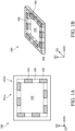
- the first semiconductor device 100 includes a seal ring 108 surrounding the first semiconductor component 102.
- the seal ring 108 may laterally enclose the first semiconductor component 102 to provide protection from water, chemicals, residue, contaminants, or the like that may be present during processing the first semiconductor component 102.
- the seal ring 108 may be formed of a conductive material, such as metal, including copper, copper alloy, or any suitable material.
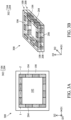
- FIG. 2A is a top view of a second semiconductor device 200 in accordance with some embodiments of the present disclosure.
- FIG. 2B is a perspective view of the second semiconductor device 200 in accordance with some embodiments of the present disclosure. Additional features can be added to the second semiconductor device 200. Some of the features described below can be replaced or eliminated for different embodiments. To simplify the diagram, only a portion of the second semiconductor device 200 is illustrated.
- the second semiconductor device 200 may include a second semiconductor component 202.
- the second semiconductor component 202 may include an active region 201a and an edge region 201b surrounding the active region 201a.
- the second semiconductor component 202 is a semiconductor die, and includes a system-on-chip (SoC) die, a logic device, a memory device, a radio frequency (RF) device, the like, or any combination thereof.
- the second semiconductor component 202 may include a micro control unit (MCU) die, a microprocessor unit (MPU) die, a power management integrated circuit (PMIC) die, a radio frequency front end (RFFE) die, an accelerated processing unit (APU) die, a central processing unit (CPU) die, a graphics processing unit (GPU) die, an input-output (IO) die, a dynamic random access memory (DRAM) controller, a static random-access memory (SRAM), a high bandwidth memory (HBM), an application processor (AP) die, an application specific integrated circuit (ASIC) die, the like, or a combination thereof.
- MCU micro control unit
- MPU microprocessor unit
- PMIC power management integrated circuit
- RFFE radio frequency front end
- APU accelerated processing unit
- the second semiconductor component 202 is an interposer.
- the interposer may include a bulk semiconductor, a compound semiconductor, an alloy semiconductor, the like, or a combination thereof, and may be formed of silicon, germanium, or any suitable semiconductor material.
- the interposer may include a wiring structure therein.
- the first semiconductor component 102 and the second semiconductor component 202 may include the same or different components.
- a semiconductor device 300 includes the first semiconductor device 100 and the second semiconductor device 200, in accordance with some embodiments.
- the first semiconductor device 100 and the second semiconductor device 200 may be stacked in the direction D3.
- the first semiconductor component 102 may be flipped upside down and disposed over the second semiconductor component 202, so that the first semiconductor component 102 and the second semiconductor component 202 may be assembled face-to-face.
- the first semiconductor device 100 may vertically overlap the second semiconductor device 200.
- the first semiconductor device 100 and the second semiconductor device 200 may include similar areas.
- the active region 101a of the first semiconductor component 102 may vertically overlap the active region 201a of the second semiconductor component 202
- the edge region 101b of the first semiconductor component 102 may vertically overlap the edge region 201b of the second semiconductor component 202.
- the first conductive paths 104 may be spaced apart from each other, and the second conductive paths 204 may be spaced apart from each other. In some embodiments, the first conductive paths 104 and the second conductive paths 204 are in a staggered arrangement. Thus, each of the first conductive paths 104 may be disposed between two of the second conductive paths 204, and each of the second conductive paths 204 may be disposed between two of the first conductive paths 104 in the top view, as shown in FIG. 3A .
- the staggered first conductive paths 104 and second conductive paths 204 may form a damage detection structure 302. As shown in FIG. 3B , the damage detection structure 302 may continuously surround the active areas of the stacked first semiconductor component 102 and second semiconductor component 202.
- FIG. 4 is a cross-sectional view of the semiconductor device 300 taken along line I-I' shown in FIG. 3A .
- two of the first conductive paths 104 may be spaced apart by one of the first dielectric layers 106
- two of the second conductive paths 204 may be spaced apart by one of the second dielectric layers 206.
- the first dielectric layers 106 and the second dielectric layers 206 are in a staggered arrangement.
- each of the second conductive paths 204 may include a plurality of conductive vias 210 and a plurality of conductive pads 212, in accordance with some embodiments.
- the conductive vias 210 and the conductive pads 212 may be formed of metal, including copper, silver, gold, the like, an alloy thereof, or a combination thereof.
- the conductive pads 212 may be disposed on the frontside surface 202f of the second semiconductor component 202.
- the conductive vias 210 may be stacked below the conductive pads 212 in the direction D3.
- the conductive vias 210 may be electrically coupled to the conductive pads 212.
- the second conductive paths 204 may include a plurality of V shapes as illustrated in FIG. 4 . Similar to the discussion of the first conductive paths 104, the second conductive paths 204 may include any suitable shapes, such as U shapes, M shapes, W shapes, ladder shapes, or the like. Therefore, the damage detection structure 302 may be in a zigzag shape across the edge regions of the stacked first semiconductor component 102 and the second semiconductor component 202, as shown in FIG. 4 .
- FIG. 5 is a perspective view of the semiconductor device 300 in accordance with some embodiments of the present disclosure. As shown in FIG. 5 , the position of each of the conductive pads 112 may corresponds to the position of each of the conductive pads 212.
- Damages in the first semiconductor component 102 and the second semiconductor component 202 may be detected through physical failure analysis (PFA).
- PFA physical failure analysis
- a signal is generated and transmitted through the damage detection structure 302, and then a disruption of the signal due to a damage is monitored. Therefore, the damages in the edge regions of the stacked first semiconductor component 102 and second semiconductor component 202 can be detected before reaching the active areas. Consequently, die damage issues and the RMA rate can be reduced.
- first conductive paths 104 is electrically coupled to the second conductive paths 204, information related to the damages in the edge region 101b of the first semiconductor component 102 and in the edge region 201b of the second semiconductor component 202 can be obtained at one time without monitoring multiple times.
- FIG. 6 is a perspective view of the semiconductor device 300 in accordance with some embodiments of the present disclosure. Only a portion of the first conductive paths 104 and the second conductive paths 204 are illustrated for simplicity. As shown in FIG. 6 , the first conductive paths 104 and the second conductive paths 204 may be in a staggered arrangement.
- the damage detection structure 302 may be in a zigzag shape, and the turning points of the zigzag shape may be adjacent to the top surface of the first semiconductor device 100 and the bottom surface of the second semiconductor device 200, respectively.
- the positions of the conductive paths 304 and the conductive terminals 306 may be adjusted.
- the conductive terminals 306 may be disposed over the top surface of the first semiconductor device 100 as illustrated in FIG. 6 .
- the conductive paths 304 may be disposed in the second semiconductor device 200, and the conductive terminals 306 may be disposed below the bottom surface of the second semiconductor device 200, as illustrated in FIG. 5 .
- the numbers of the conductive paths 304 and the conductive terminals 306 may be adjusted.
- the semiconductor device 300 may include more than two conductive paths 304 and/or more than two conductive terminals 306.
- FIG. 7 is a perspective view of the semiconductor device 400 in accordance with some embodiments of the present disclosure. It should be noted that the semiconductor device 400 may include the same or similar components as those of the semiconductor device 300, and for the sake of simplicity, those components will not be discussed in detail again. In the following embodiments, the area of the first semiconductor device 100 is different from the area of the second semiconductor device 200.
- the area of the second semiconductor device 200 may be greater than the area of the first semiconductor device 100.
- the second semiconductor device 200 may be an interposer and the first semiconductor device 100 may be a semiconductor die.
- the edge region of the second semiconductor component 202 may surround the edge region of the first semiconductor component 102 when viewing in the direction vertical to the top surface of the first semiconductor device 100.
- the conductive pads 212 may be outside of (such as surround) the conductive pads 112.
- the damage detection structure 302 include a plurality of conductive lines 402 extending along the top surface of the second semiconductor device 200, in accordance with some embodiments.
- the conductive lines 402 may electrically couple the second conductive paths 204 to the first conductive paths 104.
- the conductive lines 402 may be formed of metal, including copper, silver, gold, the like, an alloy thereof, or a combination thereof.
- the conductive lines 402 may extend below the bottom surface of the first semiconductor device 100 and may below the seal ring (such as the seal ring 108 in FIG. 3B ) of the first semiconductor device 100.
- FIG. 9 is a cross-sectional view of a semiconductor device 500 in accordance with some embodiments of the present disclosure. It should be noted that the semiconductor device 500 may include the same or similar components as that of the semiconductor device 300, and for the sake of simplicity, those components will not be discussed in detail again. In the following embodiments, more than two semiconductor components are monitored.
- the substrate 502 may be a package substrate.
- the substrate 502 may be a printed circuit board (PCB).
- the substrate 502 may include a bulk semiconductor, a compound semiconductor, an alloy semiconductor, the like, or a combination thereof, and may be formed of silicon, germanium, or any suitable semiconductor material.
- the substrate 502 may include a wiring structure therein.
- the substrate 502 may be a coreless substrate or may include an insulating core, such as a fiberglass reinforced resin core, to prevent the substrate 502 from warpage.
- the damage detection structure may further include a plurality of third conductive paths 504 and 506 disposed in the substrate 502.
- the third conductive paths 504 and 506 may electrically couple the first portion 302a to the second portion 302b of the damage detection structure.
- the semiconductor device 500 may include additional conductive paths and two or more conductive terminals (not illustrated).
- the conductive paths may be disposed in the substrate 502 and the conductive terminals may be disposed below the bottom surface of the substrate 502.
- the conductive terminals may be electrically coupled to the damage detection structure through the conductive paths. Since the damage detection structure surrounds four semiconductor components, information related to the damages in the edge regions of these semiconductor components can be monitored at one time without monitoring multiple times.
- the two stacked structures 300a and 300b are for illustrative purposes only, and more stacked structures may be disposed over the substrate 502.
- the first stacked structure 300a and/or the second stacked structure 300b may include semiconductor devices which have different areas, such as those described with reference to FIG. 8 .
- additional semiconductor components such as semiconductor dies, resistors, capacitors, or inductors may also be disposed over the substrate 502.
- the present disclosure can be applied to system on integrated chips (SoIC), integrated fan out (InFO), chip on wafer on substrate (CoWoS), 2.5-dimensional (2.5D)/three-dimensional (3D) integrated circuit (IC), or any suitable semiconductor package structure.
- SoIC system on integrated chips
- InFO integrated fan out
- CoWoS chip on wafer on substrate
- 2.5-dimensional 2.5D
- 3D three-dimensional integrated circuit
- the semiconductor device includes a damage detection structure disposed in edge regions and surround active regions of semiconductor components, so that the damages in the edge regions can be detected before reaching the active areas.
- a damage detection structure disposed in edge regions and surround active regions of semiconductor components, so that the damages in the edge regions can be detected before reaching the active areas.
- die damage issues and the RMA rate can be reduced.
- information related to the damages in the edge regions of these semiconductor components can be obtained at one time without monitoring multiple times.
- the present invention may also be defined by the following numbered clauses.
Landscapes
- Semiconductor Integrated Circuits (AREA)
- Testing Or Measuring Of Semiconductors Or The Like (AREA)
- Internal Circuitry In Semiconductor Integrated Circuit Devices (AREA)
Applications Claiming Priority (2)
| Application Number | Priority Date | Filing Date | Title |
|---|---|---|---|
| US202363615819P | 2023-12-29 | 2023-12-29 | |
| US18/961,983 US20250218875A1 (en) | 2023-12-29 | 2024-11-27 | Semiconductor device |
Publications (2)
| Publication Number | Publication Date |
|---|---|
| EP4579720A2 true EP4579720A2 (de) | 2025-07-02 |
| EP4579720A3 EP4579720A3 (de) | 2025-09-17 |
Family
ID=93926698
Family Applications (1)
| Application Number | Title | Priority Date | Filing Date |
|---|---|---|---|
| EP24222401.2A Pending EP4579720A3 (de) | 2023-12-29 | 2024-12-20 | Halbleiteranordnung |
Country Status (3)
| Country | Link |
|---|---|
| US (1) | US20250218875A1 (de) |
| EP (1) | EP4579720A3 (de) |
| CN (1) | CN120237125A (de) |
Family Cites Families (2)
| Publication number | Priority date | Publication date | Assignee | Title |
|---|---|---|---|---|
| KR20170051085A (ko) * | 2015-11-02 | 2017-05-11 | 삼성전자주식회사 | 3차원 크랙 검출 구조물을 포함하는 반도체 장치 및 크랙 검출 방법 |
| US11756842B2 (en) * | 2021-04-16 | 2023-09-12 | Taiwan Semiconductor Manufacturing Company, Ltd. | Daisy-chain seal ring structure |
-
2024
- 2024-11-27 US US18/961,983 patent/US20250218875A1/en active Pending
- 2024-12-18 CN CN202411872043.9A patent/CN120237125A/zh active Pending
- 2024-12-20 EP EP24222401.2A patent/EP4579720A3/de active Pending
Also Published As
| Publication number | Publication date |
|---|---|
| TW202537107A (zh) | 2025-09-16 |
| EP4579720A3 (de) | 2025-09-17 |
| US20250218875A1 (en) | 2025-07-03 |
| CN120237125A (zh) | 2025-07-01 |
Similar Documents
| Publication | Publication Date | Title |
|---|---|---|
| US8124456B2 (en) | Methods for securing semiconductor devices using elongated fasteners | |
| US9607947B2 (en) | Reliable microstrip routing for electronics components | |
| EP3163614A2 (de) | Gestapelte ausfächerungspackungsstruktur | |
| US20190103357A1 (en) | Methods of forming package on package assemblies with reduced z height and structures formed thereby | |
| US20240203960A1 (en) | Semiconductor package | |
| US11469189B2 (en) | Inductor and transmission line with air gap | |
| US10867951B2 (en) | Semiconductor device | |
| US9589947B2 (en) | Semiconductor packages and methods of manufacturing the same | |
| US9230897B2 (en) | Semiconductor devices having through-substrate via plugs and semiconductor packages including the same | |
| US12100635B2 (en) | Semiconductor package and method of fabricating the same | |
| US20250218875A1 (en) | Semiconductor device | |
| US20190139842A1 (en) | Semiconductor structure | |
| US20240145367A1 (en) | Semiconductor package structure | |
| CN221861635U (zh) | 一种半导体封装结构、半导体模组和电子设备 | |
| US20240136275A1 (en) | Semiconductor package structure | |
| TWI919693B (zh) | 半導體裝置 | |
| JP2025036269A (ja) | 半導体パッケージ | |
| CN117995799A (zh) | 半导体封装结构 | |
| US20230170290A1 (en) | Semiconductor package | |
| US20230282626A1 (en) | High-bandwidth package-on-package structure | |
| US20240038614A1 (en) | Semiconductor package structure | |
| EP4156260B1 (de) | Passivierungsschicht mit topologischem rissstop | |
| US20240297120A1 (en) | Semiconductor package structure | |
| US20250193997A1 (en) | Multilayer wiring substrate and semiconductor package including the multilayer wiring substrate | |
| EP4498431B1 (de) | Halbleitergehäusestruktur |
Legal Events
| Date | Code | Title | Description |
|---|---|---|---|
| PUAI | Public reference made under article 153(3) epc to a published international application that has entered the european phase |
Free format text: ORIGINAL CODE: 0009012 |
|
| STAA | Information on the status of an ep patent application or granted ep patent |
Free format text: STATUS: THE APPLICATION HAS BEEN PUBLISHED |
|
| AK | Designated contracting states |
Kind code of ref document: A2 Designated state(s): AL AT BE BG CH CY CZ DE DK EE ES FI FR GB GR HR HU IE IS IT LI LT LU LV MC ME MK MT NL NO PL PT RO RS SE SI SK SM TR |
|
| PUAL | Search report despatched |
Free format text: ORIGINAL CODE: 0009013 |
|
| AK | Designated contracting states |
Kind code of ref document: A3 Designated state(s): AL AT BE BG CH CY CZ DE DK EE ES FI FR GB GR HR HU IE IS IT LI LT LU LV MC ME MK MT NL NO PL PT RO RS SE SI SK SM TR |
|
| RIC1 | Information provided on ipc code assigned before grant |
Ipc: H01L 21/66 20060101AFI20250812BHEP Ipc: H01L 23/58 20060101ALN20250812BHEP |
|
| STAA | Information on the status of an ep patent application or granted ep patent |
Free format text: STATUS: REQUEST FOR EXAMINATION WAS MADE |
|
| 17P | Request for examination filed |
Effective date: 20260224 |