EP4579703A2 - Mehrschichtiges elektronisches bauteil mit vier äusseren elektroden und dazwischen liegendem isolierband - Google Patents
Mehrschichtiges elektronisches bauteil mit vier äusseren elektroden und dazwischen liegendem isolierband Download PDFInfo
- Publication number
- EP4579703A2 EP4579703A2 EP24219131.0A EP24219131A EP4579703A2 EP 4579703 A2 EP4579703 A2 EP 4579703A2 EP 24219131 A EP24219131 A EP 24219131A EP 4579703 A2 EP4579703 A2 EP 4579703A2
- Authority
- EP
- European Patent Office
- Prior art keywords
- electrode
- lead portion
- internal electrode
- exposed
- dummy electrode
- Prior art date
- Legal status (The legal status is an assumption and is not a legal conclusion. Google has not performed a legal analysis and makes no representation as to the accuracy of the status listed.)
- Pending
Links
Images




Classifications
-
- H—ELECTRICITY
- H01—ELECTRIC ELEMENTS
- H01G—CAPACITORS; CAPACITORS, RECTIFIERS, DETECTORS, SWITCHING DEVICES, LIGHT-SENSITIVE OR TEMPERATURE-SENSITIVE DEVICES OF THE ELECTROLYTIC TYPE
- H01G4/00—Fixed capacitors; Processes of their manufacture
- H01G4/30—Stacked capacitors
-
- H—ELECTRICITY
- H01—ELECTRIC ELEMENTS
- H01G—CAPACITORS; CAPACITORS, RECTIFIERS, DETECTORS, SWITCHING DEVICES, LIGHT-SENSITIVE OR TEMPERATURE-SENSITIVE DEVICES OF THE ELECTROLYTIC TYPE
- H01G4/00—Fixed capacitors; Processes of their manufacture
- H01G4/002—Details
- H01G4/005—Electrodes
-
- H—ELECTRICITY
- H01—ELECTRIC ELEMENTS
- H01G—CAPACITORS; CAPACITORS, RECTIFIERS, DETECTORS, SWITCHING DEVICES, LIGHT-SENSITIVE OR TEMPERATURE-SENSITIVE DEVICES OF THE ELECTROLYTIC TYPE
- H01G4/00—Fixed capacitors; Processes of their manufacture
- H01G4/002—Details
- H01G4/005—Electrodes
- H01G4/012—Form of non-self-supporting electrodes
-
- H—ELECTRICITY
- H01—ELECTRIC ELEMENTS
- H01G—CAPACITORS; CAPACITORS, RECTIFIERS, DETECTORS, SWITCHING DEVICES, LIGHT-SENSITIVE OR TEMPERATURE-SENSITIVE DEVICES OF THE ELECTROLYTIC TYPE
- H01G4/00—Fixed capacitors; Processes of their manufacture
- H01G4/002—Details
- H01G4/228—Terminals
- H01G4/232—Terminals electrically connecting two or more layers of a stacked or rolled capacitor
-
- H—ELECTRICITY
- H01—ELECTRIC ELEMENTS
- H01G—CAPACITORS; CAPACITORS, RECTIFIERS, DETECTORS, SWITCHING DEVICES, LIGHT-SENSITIVE OR TEMPERATURE-SENSITIVE DEVICES OF THE ELECTROLYTIC TYPE
- H01G4/00—Fixed capacitors; Processes of their manufacture
- H01G4/002—Details
- H01G4/018—Dielectrics
- H01G4/06—Solid dielectrics
- H01G4/08—Inorganic dielectrics
- H01G4/12—Ceramic dielectrics
Definitions
- the present disclosure relates to a multilayer electronic component.
- Multilayer Ceramic Capacitors as multilayer electronic components, are chip-type capacitors mounted on printed circuit boards of various electronic products, such as imaging devices, for example, liquid crystal displays (LCDs) and plasma display panels (PDPs), computers, smartphones, mobile phones and the like, and serve to charge or discharge electricity.
- imaging devices for example, liquid crystal displays (LCDs) and plasma display panels (PDPs)
- LCDs liquid crystal displays
- PDPs plasma display panels
- computers smartphones, mobile phones and the like, and serve to charge or discharge electricity.
- Such multilayer ceramic capacitors may be used as components in various electronic devices due to their small size, high capacitance, and ease of mounting. As various electronic devices such as computers and mobile devices are miniaturized and have higher output, the demand for miniaturization and higher capacitance for multilayer ceramic capacitors is increasing.
- multi-terminal MLCCs are sometimes used instead of the typical two-terminal MLCCs, and among these, three-terminal MLCCs have a structure in which signal patterns and ground patterns of different shapes are alternately laminated.
- a short-width external electrode should be exposed laterally, and a signal pattern, in which the external electrode is not exposed in the same direction, is laminated alternately, thereby generating a step portion.
- a decrease in the density of the step portion during lamination and compression may cause delamination.
- Such delamination may provide a moisture penetration path, whichcan cause decrease reliability.
- a structure that significantly reduces the step portion by changing the shape of a dummy electrode or lead portion is adopted.
- An aspect of the present disclosure is to provide a multilayer electronic component with improved step portion height.
- An aspect of the present disclosure is to provide a multilayer electronic component with improved moisture resistance reliability.
- a multilayer electronic component includes a body comprising a dielectric layer and first and second internal electrode layers alternately disposed with the dielectric layer therebetween in a first direction, and including a first surface and a second surface opposing each other in the first direction, a third surface and a fourth surface connected to the first and second surfaces and opposing each other in a second direction, and a fifth surface and a sixth surface connected to the first to fourth surfaces and opposing each other in a third direction, the first internal electrode layer including a first internal electrode exposed to the fifth and sixth surfaces, and a first dummy electrode disposed to be spaced apart from the first internal electrode, and the second internal electrode layer including a second internal electrode exposed to the third and fourth surfaces, and a second dummy electrode disposed to be spaced apart from the second internal electrode; a first external electrode and a second external electrode disposed on the third and fourth surfaces, respectively, and connected to the second internal electrode; a third external electrode and a fourth external electrode disposed on the fifth and sixth surfaces
- a multilayer electronic component includes a body comprising a dielectric layer and first and second internal electrode layers alternately disposed with the dielectric layer therebetween in a first direction, and having a first surface and a second surface opposing each other in the first direction, a third surface and a fourth surface connected to the first and second surfaces and opposing each other in a second direction, and a fifth surface and a sixth surface connected to the first to fourth surfaces and opposing each other in a third direction.
- the first internal electrode layer includes a first internal electrode exposed to the fifth and sixth surfaces and a first dummy electrode disposed spaced apart from the first internal electrode
- the second internal electrode layer includes a second internal electrode exposed to the third to sixth surfaces and a second dummy electrode disposed spaced apart from the second internal electrode.
- a first external electrode is disposed on the third, fifth, and sixth surfaces and connected to at least an exposed portion of the second internal electrode
- a second external electrode is disposed on the fourth, fifth, and sixth surfaces and connected to the second internal electrode
- a third external electrode is disposed on the fifth surface and connected to the first internal electrode
- a fourth external electrode is disposed on the sixth surface and connected to the first internal electrode.
- the first dummy electrode overlaps an exposed portion of the second internal electrode in the first direction
- the second dummy electrode overlaps an exposed portion of the first internal electrode in the first direction.
- the first direction may be defined as the stacking direction or the thickness (T) direction
- the second direction may be defined as the length (L) direction
- the third direction may be defined as the width (W) direction.
- FIG. 1 schematically illustrates a perspective view of a multilayer electronic component according to an embodiment.
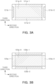
- FIGS. 3A and 3B are perspective views schematically illustrating an internal electrode layer of an embodiment.
- the plurality of dielectric layers 111 forming the body 110 are in a fired state, and the boundary between adjacent dielectric layers 111 is unified to the extent that it is difficult to confirm without using a scanning electron microscope (SEM).
- SEM scanning electron microscope
- the thickness of the dielectric layer 111 may be 10.0 um or less.
- the thickness of the dielectric layer 111 may be 3.0 um or less, and to more easily obtain ultra-miniaturization and high capacitance, the thickness of the dielectric layer 111 may be 1.0 um or less, in detail, 0.6 um or less, and more specifically, 0.4 um or less.
- the thickness of the dielectric layer 111 refers to the thickness of the dielectric layer 111 disposed between the first and second internal electrode layers 121 and 122.
- the thickness of the dielectric layer 111 refers to the size of the dielectric layer 111 in the first direction.
- the thickness of the dielectric layer 111 refers to the average thickness of the dielectric layer 111 and refers to the average size of the dielectric layer 111 in the first direction.
- the internal electrode layers 121 and 122 include a first internal electrode layer 121 and a second internal electrode layer 122, and the first and second internal electrode layers 121 and 122 are alternately disposed in the first direction with the dielectric layer 111 constituting the body 110, interposed therebetween.
- the second internal electrode 122a is spaced apart from the fifth and sixth surfaces 5 and 6 and exposed through the third and fourth surfaces 3 and 4 to be connected to the first and second external electrodes 131 and 132, and the second dummy electrode 122b is exposed through the fifth and sixth surfaces 5 and 6 to be connected to the third and fourth external electrodes 133 and 134.
- the first internal electrode 121a is not connected to the first and second external electrodes 131 and 132 and is connected to the third and fourth external electrodes 133 and 134
- the second internal electrode 122a is not connected to the third and fourth external electrodes 133 and 134 but may be connected to the first and second external electrodes 131 and 132.
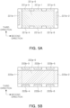
- the first and second internal electrodes 121a and 122a may be electrically isolated from each other by a dielectric layer 111 disposed between them in the first direction, and may include main portions 121a-0 and 122a-0 that form a capacitance by overlapping in the first direction and lead portions 121a-1, 121a-2, 122a-1 and 122a-2, which do not form a capacitance and are exposed to one surface of the body.
- the lead portion of the internal electrode exposed to one surface of the body is not limited to one, but may include multiple lead portions. This will be described in more detail below.
- first dummy electrode 121b may overlap the exposed portions 122a-1 and 122a-2 of the second internal electrode 122a in the first direction
- second dummy electrode 122b may overlap the exposed portions 121a-1 and 121a-2 of the first internal electrode 121a in the first direction.
- the step portion in the area where the capacitance is not formed may be significantly reduced, and the process work may be simplified when applying the paste, thereby improving the process speed.
- first and second internal electrodes 121a and 122a may have substantially constant sizes in the second direction and substantially constant sizes in the third direction, respectively.
- the areas 121a-1, 121a-2, 122a-1 and 122a-2 exposed through one surface of the body among the first and second internal electrodes may have substantially constant sizes in the second direction and substantially constant sizes in the third direction, respectively.
- substantially constant sizes in the second direction may mean that the second direction sizes are 5% or less based on the average value of the second direction maximum size and the second direction minimum size, and this definition also applies to the substantially constant sizes in the third direction
- the body 110 may be formed by alternately stacking a first ceramic green sheet on which a first internal electrode layer 121 is printed and a second ceramic green sheet on which a second internal electrode layer 122 is printed, and then firing the stack.
- the internal electrode layers 121 and 122 are not particularly limited, and materials with excellent electrical conductivity may be used.
- the internal electrode layers 121 and 122 may include at least one of nickel (Ni), copper (Cu), palladium (Pd), silver (Ag), gold (Au), platinum (Pt), tin (Sn), tungsten (W), titanium (Ti) and alloys thereof.
- the internal electrode layers 121 and 122 may be formed by printing a conductive paste for internal electrodes, containing at least one of nickel (Ni), copper (Cu), palladium (Pd), silver (Ag), gold (Au), platinum (Pt), tin (Sn), tungsten (W), titanium (Ti) and alloys thereof, onto a ceramic green sheet.
- the printing method for the conductive paste for internal electrodes may be screen printing or gravure printing, and the present disclosure is not limited thereto.
- the thickness of the internal electrode layers 121 and 122 does not need to be particularly limited.
- the thickness of the internal electrode layers 121 and 122 may be 3.0 um or less.
- the thickness of the internal electrode layers 121 and 122 may be 1.0 um or less, and to more easily obtain ultra-miniaturization and high capacitance, the thickness of the internal electrode layers 121 and 122 may be 0.6 um or less, and more specifically, 0.4 um or less.
- the thickness of the internal electrode layers 121 and 122 refers to the size of the internal electrode layers 121 and 122 in the first direction.
- the thickness of the internal electrode layers 121 and 122 refers to the average thickness of the internal electrode layers 121 and 122 or the average size in the first direction .
- the first direction average size of the internal electrode layers 121 and 122 may be measured by scanning the cross-sectional image of the body 110 in the first and second directions with a scanning electron microscope (SEM) at 10,000x magnification.
- the first direction average size of one internal electrode layer is an average value calculated by measuring the first direction size of one internal electrode layer at 10 equally spaced points in the second direction in the scanned image. The 10 equally spaced points are designated in the capacitance formation portion.
- this average value measurement is extended to 10 internal electrode layers and the average value is measured, the first direction average size of the internal electrode layers may be more generalized.
- the average thickness td of one dielectric layer 111 may be greater than twice the average thickness te of one of the internal electrode layers 121 and 122.
- the average thickness td of the plurality of dielectric layers 111 may be greater than twice the average thickness te of the plurality of internal electrode layers 121 and 122.
- BDV breakdown voltage
- the average thickness td of the dielectric layer 111 may be greater than twice the average thickness te of the internal electrode layers 121 and 122, thereby increasing the thickness of the dielectric layer, which is the distance between the internal electrode layers, and improving the breakdown voltage characteristics.
- the average thickness td of the dielectric layer 111 is twice or less than twice the average thickness te of the internal electrode layers 121 and 122, the average thickness of the dielectric layer, which is the distance between the internal electrode layers, may be too thin. Thus, the breakdown voltage may deteriorate, and a short circuit could occur between the internal electrode layers.
- the body 110 may include a cover portion disposed on both end surfaces of the capacitance formation portion in the first direction.
- the body 110 may include a first cover portion disposed on one surface of the capacitance formation portion in the first direction and a second cover portion disposed on the other surface of the capacitance formation portion in the first direction, and in more detail, may include an upper cover portion disposed on the upper portion of the capacitance formation portion in the first direction and a lower cover portion disposed on the lower portion of the capacitance formation portion in the first direction.
- the average size of the cover portion in the first direction may be measured by scanning an image of the cross-section of the body 110 in the first and second directions with a scanning electron microscope (SEM) at 10,000x magnification. More specifically it refers to an average value calculated by measuring the first direction size at 10 points equally spaced in the second direction in an image obtained by scanning one cover portion.
- SEM scanning electron microscope
- the first direction average size of the cover portion measured by the above-described method may have a size substantially equal to the first direction average size of the cover portion in the first and third direction cross-section of the body 110.
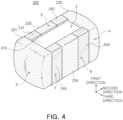
- the external electrodes 131 and 132 may include a first external electrode 131 disposed on the third surface 3 of the body 110 and connected to the second internal electrode 122a, a second external electrode 132 disposed on the fourth surface 4 of the body 110 and connected to the second internal electrode 122a, a third external electrode 133 disposed on the fifth surface 5 of the body 110 and connected to the first internal electrode 121a, and a fourth external electrode 134 disposed on the sixth surface 6 of the body 110 and connected to the first internal electrode 121a.
- the third and fourth external electrodes 133 and 134 may be disposed to extend to portions of the first and second surfaces 1 and 2 of the body 110.
- the third external electrode 133 may be disposed on portions of the first and second surfaces 1 and 2 of the body 110 and on the fifth surface 5 of the body 110
- the fourth external electrode 134 may be disposed on portions of the first and second surfaces 1 and 2 of the body 110 and on the sixth surface 6 of the body 110.
- the external electrodes 131, 132, 133 and 134 may be formed using may be formed using any electrically conductive material, such as metal, and a detailed material may be determined in consideration of electrical characteristics, structural stability, or the like, and may also have a multilayer structure.
- the external electrodes 131, 132, 133 and 134 may include an electrode layer disposed on the body 110 and a plating layer disposed on the electrode layer.
- the electrode layer may include a first electrode layer, which is a fired electrode composed of a first conductive metal and glass, or a second electrode layer, which is a resin-based electrode including a second conductive metal and resin.
- the conductive metal included in the first electrode layer may be referred to as a first conductive metal
- the conductive metal included in the second electrode layer may be referred to as a second conductive metal.
- the first conductive metal and the second conductive metal may be the same or different from each other, and in the case of including a plurality of conductive metals, only some thereof may include the same conductive metal, but the present disclosure is not particularly limited thereto.
- the electrode layer may be in the form of a fired electrode and a resin-based electrode sequentially formed on the body 110.
- the electrode layer may be formed by transferring a sheet containing a conductive metal onto the body, or may be formed by transferring a sheet containing a conductive metal onto a fired electrode.
- a material with excellent electrical conductivity may be used as the conductive metal included in the electrode layer, and for example, the conductive metal may consist of at least one selected from the group consisting of nickel (Ni), copper (Cu), palladium (Pd), silver (Ag), gold (Au), platinum (Pt), tin (Sn), tungsten (W), titanium (Ti), and alloys thereof, but is not particularly limited thereto.
- the electrode layer may have a two-layer structure including a first electrode layer and a second electrode layer, and accordingly, the external electrodes 131, 132, 133 and 134 may include a first electrode layer including a first conductive metal and glass, and a second electrode layer disposed on the first electrode layer and including a second conductive metal and resin.
- the first electrode layer may play a role in improving bonding with the body 110 by including glass, and the second electrode layer plays a role in improving bending strength by including resin.
- the first conductive metal included in the first electrode layer is not particularly limited as long as it is a material that may be electrically connected to the internal electrode layers 121 and 122 for forming capacitance, and may include, for example, at least one selected from the group consisting of nickel (Ni), copper (Cu), palladium (Pd), silver (Ag), gold (Au), platinum (Pt), tin (Sn), tungsten (W), titanium (Ti), and alloys thereof.
- the first electrode layer may be formed by applying a conductive paste prepared by adding glass frit to the first conductive metal particles and then firing the mixture.
- the second conductive metal included in the second electrode layer may play a role in electrically connecting with the first electrode layer.
- the conductive metal included in the second electrode layer is not particularly limited as long as it is a material that may be electrically connected to the electrode layer, and may include at least one selected from the group consisting of nickel (Ni), copper (Cu), palladium (Pd), silver (Ag), gold (Au), platinum (Pt), tin (Sn), tungsten (W), titanium (Ti), and alloys thereof.
- the second conductive metal included in the second electrode layer may include at least one of spherical particles or flake-shaped particles.
- the second conductive metal may be composed solely of flake-shaped particles, solelyof spherical particles, or a mixture of flake-shaped particles and spherical particles.
- the spherical particles may also include a shape other than a perfect spherical shape, and for example, may include a shape having a length ratio of the major axis to the minor axis (major axis/minor axis) of 1.45 or less.
- the flake-shaped particles refer to particles having a flat and elongated shape, and although not particularly limited, for example, the length ratio of the major axis to the minor axis (major axis/minor axis) may be 1.95 or more.
- the lengths of the major and minor axes of the above spherical particles and flake-shaped particles may be measured from images obtained by scanning the first and second cross-sections cut from the central portion of the multilayer electronic component in the third direction using a scanning electron microscope (SEM).
- the resin included in the second electrode layer plays the role of securing bonding properties and absorbing shocks.
- the resin included in the second electrode layer is not particularly limited as long as it has bonding properties and shock absorbing properties and may be mixed with the second conductive metal particles to form a paste, and may include, for example, an epoxy-based resin.
- the second electrode layer may include a plurality of second conductive metal particles, an intermetallic compound, and a resin.
- the intermetallic compound By including the intermetallic compound, the electrical connectivity with the first electrode layer may be further improved.
- the intermetallic compound connects multiple metal particles to improve electrical connectivity, and may surround and bind multiple metal particles.
- the intermetallic compound may include a metal having a melting point lower than the curing temperature of the resin.
- the metal having a melting point lower than the curing temperature of the resin melts during the drying and curing process, forms an intermetallic compound with some of the metal particles, and surrounds the metal particles.
- the intermetallic compound may include a low melting point metal of 300°C or less.
- Sn with a melting point of 213 to 220°C may be included.
- Sn is melted, and the melted Sn wets high-melting-point metal particles such as Ag, Ni or Cu by capillary action, and reacts with some of the Ag, Ni or Cu metal particles to form intermetallic compounds such as Ag 3 Sn, Ni 3 Sn 4 , Cu 6 Sn 5 , Cu 3 Sn, and the like.
- Ag, Ni or Cu that does not participate in the reaction remains in the form of metal particles.
- the plurality of second conductive metal particles may include at least one of Ag, Ni or Cu
- the intermetallic compound may include at least one of Ag 3 Sn, Ni 3 Sn 4 , Cu 6 Sn 5 or Cu 3 Sn.
- the plating layer plays a role in improving mounting characteristics.
- the type of plating layer is not particularly limited and may be plating layers 131c and 132c of a single layer containing at least one of nickel (Ni), tin (Sn), silver (Ag), palladium (Pd), or alloys thereof, or may be formed of multiple layers.
- the plating layer may be a Ni plating layer or a Sn plating layer, and may be in the form in which a Ni plating layer and a Sn plating layer are formed sequentially on the electrode layer. Alternatively, it may be in the form where the Sn plating layer, Ni plating layer, and Sn plating layer are formed sequentially. Additionally, the plating layer may include a plurality of Ni plating layers and/or a plurality of Sn plating layers.
- An embodiment may include an insulating portion 141, 142, 143 and 144 disposed on a body 110.
- the first and second insulating portions 141 and 142 may be connected to the lead portion 121a-1 of the first internal electrode and the first dummy electrode 122b-1, which are exposed on the fifth surface 5, respectively, and the third and fourth insulating portions 143 and 144 may be connected to the lead portion 121a-2 of the first internal electrode and the first dummy electrode 122b-2, exposed to the sixth surface 6, respectively.
- the insulating portions 141, 142, 143 and 144 are disposed to cover the internal electrode layers 121 and 122 exposed on one surface of the body, external moisture penetration may be suppressed, thereby improving moisture resistance reliability.
- the size of the third and fourth external electrodes 133 and 134 is reduced, and thus, even when the area of the exposed internal electrode layers 121 and 122 increases, the area may be sufficiently covered by the insulating portions 141, 142, 143 and 144. Therefore, the area of the mounted pad may be significantly reduced while also providing excellent moisture resistance reliability.
- the thickness of the dielectric layer and the internal electrode should be reduced to increase the number of layers, and thus, the effect according to the present disclosure may be more significant in a multilayer electronic component 100 having a size of 3216 (length ⁇ width: 3.2 mm ⁇ 1.6 mm) or less.
- a multilayer electronic component 100 includes a body 110 including a dielectric layer 111 and first and second internal electrode layers 121 and 122 alternately disposed in a first direction with the dielectric layer 111 interposed between them, and including first and second surfaces 1 and 2 opposing each other in the first direction, third and fourth surfaces 3 and 4 connected to the first and second surfaces 1 and 2 and opposing each other in the second direction, and fifth and sixth surfaces 5 and 6 connected to the first to fourth surfaces 1, 2, 3, and 4 and opposing each other in the third direction, the first internal electrode layer 121 including a first internal electrode 121a exposed to the fifth and sixth surfaces 5 and 6 and a first dummy electrode 121b disposed spaced apart from the first internal electrode 121a, and the second internal electrode layer 122 including a second internal electrode 122a exposed to the third and fourth surfaces 3 and 4 and a second dummy electrode 122b spaced apart from the second internal electrode 122a; first and second external electrodes 131 and 132 disposed on the third and fourth surfaces 3 and 4, respectively, and connected
- a multilayer electronic component 400 may include the same configuration as the multilayer electronic components 100, 200 and 300 except that it does not include an insulating portion, and the same configuration or description excluding the insulating portion will be omitted, but those skilled in the art will be able to easily understand it.
- the step portion of a multilayer electronic component is improved.
Landscapes
- Engineering & Computer Science (AREA)
- Power Engineering (AREA)
- Manufacturing & Machinery (AREA)
- Microelectronics & Electronic Packaging (AREA)
- Fixed Capacitors And Capacitor Manufacturing Machines (AREA)
- Ceramic Capacitors (AREA)
- Ceramic Engineering (AREA)
- Chemical & Material Sciences (AREA)
- Inorganic Chemistry (AREA)
Applications Claiming Priority (1)
| Application Number | Priority Date | Filing Date | Title |
|---|---|---|---|
| KR1020230197086A KR20250104555A (ko) | 2023-12-29 | 2023-12-29 | 적층형 전자 부품 |
Publications (2)
| Publication Number | Publication Date |
|---|---|
| EP4579703A2 true EP4579703A2 (de) | 2025-07-02 |
| EP4579703A3 EP4579703A3 (de) | 2025-11-19 |
Family
ID=93893414
Family Applications (1)
| Application Number | Title | Priority Date | Filing Date |
|---|---|---|---|
| EP24219131.0A Pending EP4579703A3 (de) | 2023-12-29 | 2024-12-11 | Mehrschichtiges elektronisches bauteil mit vier äusseren elektroden und dazwischen liegendem isolierband |
Country Status (5)
| Country | Link |
|---|---|
| US (1) | US20250218690A1 (de) |
| EP (1) | EP4579703A3 (de) |
| JP (1) | JP2025105516A (de) |
| KR (1) | KR20250104555A (de) |
| CN (1) | CN120236906A (de) |
Family Cites Families (6)
| Publication number | Priority date | Publication date | Assignee | Title |
|---|---|---|---|---|
| JP2012156315A (ja) * | 2011-01-26 | 2012-08-16 | Murata Mfg Co Ltd | 積層セラミック電子部品 |
| JP2013051392A (ja) * | 2011-08-02 | 2013-03-14 | Murata Mfg Co Ltd | 積層セラミック電子部品 |
| KR101525645B1 (ko) * | 2011-09-02 | 2015-06-03 | 삼성전기주식회사 | 적층 세라믹 커패시터 |
| US20150021082A1 (en) * | 2013-07-17 | 2015-01-22 | Samsung Electro-Mechanics Co., Ltd. | Multilayer ceramic capacitor and board having the same |
| KR102613871B1 (ko) | 2016-11-23 | 2023-12-15 | 삼성전기주식회사 | 적층형 커패시터 및 그 실장 기판 |
| US12512269B2 (en) * | 2021-12-29 | 2025-12-30 | Samsung Electro-Mechanics Co., Ltd. | Multilayer electronic component |
-
2023
- 2023-12-29 KR KR1020230197086A patent/KR20250104555A/ko active Pending
-
2024
- 2024-12-11 EP EP24219131.0A patent/EP4579703A3/de active Pending
- 2024-12-17 JP JP2024221193A patent/JP2025105516A/ja active Pending
- 2024-12-23 US US18/999,486 patent/US20250218690A1/en active Pending
- 2024-12-26 CN CN202411936547.2A patent/CN120236906A/zh active Pending
Also Published As
| Publication number | Publication date |
|---|---|
| JP2025105516A (ja) | 2025-07-10 |
| EP4579703A3 (de) | 2025-11-19 |
| KR20250104555A (ko) | 2025-07-08 |
| US20250218690A1 (en) | 2025-07-03 |
| CN120236906A (zh) | 2025-07-01 |
Similar Documents
| Publication | Publication Date | Title |
|---|---|---|
| US8310805B2 (en) | Multilayer ceramic electronic component including plating material of external terminal electrode disposed in voids of inner conductor and method for manufacturing the same | |
| CN109473279B (zh) | 多层陶瓷电容器及其制造方法 | |
| US20190385797A1 (en) | Multilayer ceramic electronic component and board for mounting of the same | |
| US11551875B2 (en) | Multilayer ceramic electronic component | |
| US11217393B2 (en) | Capacitor component | |
| CN111180201B (zh) | 多层陶瓷电子组件 | |
| US11776746B2 (en) | Multilayer capacitor | |
| US12603229B2 (en) | Multilayered electronic component | |
| US20250132093A1 (en) | Multilayer electronic component | |
| EP4579703A2 (de) | Mehrschichtiges elektronisches bauteil mit vier äusseren elektroden und dazwischen liegendem isolierband | |
| US12136518B2 (en) | Multilayer electronic component including cover layer having insulating and conductive portions | |
| US20250218672A1 (en) | Multilayer electronic component | |
| KR20220121025A (ko) | 적층 세라믹 전자부품 | |
| US20250166914A1 (en) | Multilayer electronic component | |
| US20250054700A1 (en) | Multilayer electronic component | |
| EP4560660A1 (de) | Mehrschichtiges elektronisches bauteil | |
| US20250385048A1 (en) | Multilayer electronic component | |
| JP2025084714A (ja) | 積層型電子部品 | |
| KR20170077532A (ko) | 내부전극용 도전성 페이스트 및 적층 세라믹 전자부품의 제조방법 |
Legal Events
| Date | Code | Title | Description |
|---|---|---|---|
| PUAI | Public reference made under article 153(3) epc to a published international application that has entered the european phase |
Free format text: ORIGINAL CODE: 0009012 |
|
| STAA | Information on the status of an ep patent application or granted ep patent |
Free format text: STATUS: THE APPLICATION HAS BEEN PUBLISHED |
|
| AK | Designated contracting states |
Kind code of ref document: A2 Designated state(s): AL AT BE BG CH CY CZ DE DK EE ES FI FR GB GR HR HU IE IS IT LI LT LU LV MC ME MK MT NL NO PL PT RO RS SE SI SK SM TR |
|
| REG | Reference to a national code |
Ref country code: DE Ref legal event code: R079 Free format text: PREVIOUS MAIN CLASS: H01G0004012000 Ipc: H01G0004300000 |
|
| PUAL | Search report despatched |
Free format text: ORIGINAL CODE: 0009013 |
|
| AK | Designated contracting states |
Kind code of ref document: A3 Designated state(s): AL AT BE BG CH CY CZ DE DK EE ES FI FR GB GR HR HU IE IS IT LI LT LU LV MC ME MK MT NL NO PL PT RO RS SE SI SK SM TR |
|
| RIC1 | Information provided on ipc code assigned before grant |
Ipc: H01G 4/30 20060101AFI20251016BHEP Ipc: H01G 4/012 20060101ALI20251016BHEP Ipc: H01G 4/232 20060101ALI20251016BHEP Ipc: H01G 4/12 20060101ALN20251016BHEP |
|
| STAA | Information on the status of an ep patent application or granted ep patent |
Free format text: STATUS: REQUEST FOR EXAMINATION WAS MADE |
|
| 17P | Request for examination filed |
Effective date: 20260320 |